WO2022201615A1 - 電子回路モジュール - Google Patents
電子回路モジュール Download PDFInfo
- Publication number
- WO2022201615A1 WO2022201615A1 PCT/JP2021/039525 JP2021039525W WO2022201615A1 WO 2022201615 A1 WO2022201615 A1 WO 2022201615A1 JP 2021039525 W JP2021039525 W JP 2021039525W WO 2022201615 A1 WO2022201615 A1 WO 2022201615A1
- Authority
- WO
- WIPO (PCT)
- Prior art keywords
- recess
- heat
- substrate
- filler
- sealing resin
- Prior art date
- Legal status (The legal status is an assumption and is not a legal conclusion. Google has not performed a legal analysis and makes no representation as to the accuracy of the status listed.)
- Ceased
Links
Images





Classifications
-
- H—ELECTRICITY
- H05—ELECTRIC TECHNIQUES NOT OTHERWISE PROVIDED FOR
- H05K—PRINTED CIRCUITS; CASINGS OR CONSTRUCTIONAL DETAILS OF ELECTRIC APPARATUS; MANUFACTURE OF ASSEMBLAGES OF ELECTRICAL COMPONENTS
- H05K1/00—Printed circuits
- H05K1/02—Details
- H05K1/0201—Thermal arrangements, e.g. for cooling, heating or preventing overheating
- H05K1/0203—Cooling of mounted components
- H05K1/0204—Cooling of mounted components using means for thermal conduction connection in the thickness direction of the substrate
-
- H—ELECTRICITY
- H10—SEMICONDUCTOR DEVICES; ELECTRIC SOLID-STATE DEVICES NOT OTHERWISE PROVIDED FOR
- H10W—GENERIC PACKAGES, INTERCONNECTIONS, CONNECTORS OR OTHER CONSTRUCTIONAL DETAILS OF DEVICES COVERED BY CLASS H10
- H10W90/00—Package configurations
-
- H—ELECTRICITY
- H05—ELECTRIC TECHNIQUES NOT OTHERWISE PROVIDED FOR
- H05K—PRINTED CIRCUITS; CASINGS OR CONSTRUCTIONAL DETAILS OF ELECTRIC APPARATUS; MANUFACTURE OF ASSEMBLAGES OF ELECTRICAL COMPONENTS
- H05K1/00—Printed circuits
- H05K1/02—Details
- H05K1/0201—Thermal arrangements, e.g. for cooling, heating or preventing overheating
- H05K1/0203—Cooling of mounted components
- H05K1/0209—External configuration of printed circuit board adapted for heat dissipation, e.g. lay-out of conductors, coatings
-
- H—ELECTRICITY
- H05—ELECTRIC TECHNIQUES NOT OTHERWISE PROVIDED FOR
- H05K—PRINTED CIRCUITS; CASINGS OR CONSTRUCTIONAL DETAILS OF ELECTRIC APPARATUS; MANUFACTURE OF ASSEMBLAGES OF ELECTRICAL COMPONENTS
- H05K1/00—Printed circuits
- H05K1/02—Details
- H05K1/0266—Marks, test patterns or identification means
-
- H—ELECTRICITY
- H05—ELECTRIC TECHNIQUES NOT OTHERWISE PROVIDED FOR
- H05K—PRINTED CIRCUITS; CASINGS OR CONSTRUCTIONAL DETAILS OF ELECTRIC APPARATUS; MANUFACTURE OF ASSEMBLAGES OF ELECTRICAL COMPONENTS
- H05K1/00—Printed circuits
- H05K1/18—Printed circuits structurally associated with non-printed electric components
- H05K1/181—Printed circuits structurally associated with non-printed electric components associated with surface mounted components
-
- H—ELECTRICITY
- H10—SEMICONDUCTOR DEVICES; ELECTRIC SOLID-STATE DEVICES NOT OTHERWISE PROVIDED FOR
- H10P—GENERIC PROCESSES OR APPARATUS FOR THE MANUFACTURE OR TREATMENT OF DEVICES COVERED BY CLASS H10
- H10P95/00—Generic processes or apparatus for manufacture or treatments not covered by the other groups of this subclass
-
- H—ELECTRICITY
- H10—SEMICONDUCTOR DEVICES; ELECTRIC SOLID-STATE DEVICES NOT OTHERWISE PROVIDED FOR
- H10W—GENERIC PACKAGES, INTERCONNECTIONS, CONNECTORS OR OTHER CONSTRUCTIONAL DETAILS OF DEVICES COVERED BY CLASS H10
- H10W46/00—Marks applied to devices, e.g. for alignment or identification
-
- H—ELECTRICITY
- H05—ELECTRIC TECHNIQUES NOT OTHERWISE PROVIDED FOR
- H05K—PRINTED CIRCUITS; CASINGS OR CONSTRUCTIONAL DETAILS OF ELECTRIC APPARATUS; MANUFACTURE OF ASSEMBLAGES OF ELECTRICAL COMPONENTS
- H05K2201/00—Indexing scheme relating to printed circuits covered by H05K1/00
- H05K2201/02—Fillers; Particles; Fibers; Reinforcement materials
- H05K2201/0203—Fillers and particles
- H05K2201/0206—Materials
- H05K2201/0212—Resin particles
-
- H—ELECTRICITY
- H05—ELECTRIC TECHNIQUES NOT OTHERWISE PROVIDED FOR
- H05K—PRINTED CIRCUITS; CASINGS OR CONSTRUCTIONAL DETAILS OF ELECTRIC APPARATUS; MANUFACTURE OF ASSEMBLAGES OF ELECTRICAL COMPONENTS
- H05K2201/00—Indexing scheme relating to printed circuits covered by H05K1/00
- H05K2201/07—Electric details
- H05K2201/0707—Shielding
- H05K2201/0715—Shielding provided by an outer layer of PCB
-
- H—ELECTRICITY
- H10—SEMICONDUCTOR DEVICES; ELECTRIC SOLID-STATE DEVICES NOT OTHERWISE PROVIDED FOR
- H10W—GENERIC PACKAGES, INTERCONNECTIONS, CONNECTORS OR OTHER CONSTRUCTIONAL DETAILS OF DEVICES COVERED BY CLASS H10
- H10W46/00—Marks applied to devices, e.g. for alignment or identification
- H10W46/101—Marks applied to devices, e.g. for alignment or identification characterised by the type of information, e.g. logos or symbols
-
- H—ELECTRICITY
- H10—SEMICONDUCTOR DEVICES; ELECTRIC SOLID-STATE DEVICES NOT OTHERWISE PROVIDED FOR
- H10W—GENERIC PACKAGES, INTERCONNECTIONS, CONNECTORS OR OTHER CONSTRUCTIONAL DETAILS OF DEVICES COVERED BY CLASS H10
- H10W46/00—Marks applied to devices, e.g. for alignment or identification
- H10W46/101—Marks applied to devices, e.g. for alignment or identification characterised by the type of information, e.g. logos or symbols
- H10W46/106—Marks applied to devices, e.g. for alignment or identification characterised by the type of information, e.g. logos or symbols digital information, e.g. bar codes
-
- H—ELECTRICITY
- H10—SEMICONDUCTOR DEVICES; ELECTRIC SOLID-STATE DEVICES NOT OTHERWISE PROVIDED FOR
- H10W—GENERIC PACKAGES, INTERCONNECTIONS, CONNECTORS OR OTHER CONSTRUCTIONAL DETAILS OF DEVICES COVERED BY CLASS H10
- H10W46/00—Marks applied to devices, e.g. for alignment or identification
- H10W46/401—Marks applied to devices, e.g. for alignment or identification for identification or tracking
-
- H—ELECTRICITY
- H10—SEMICONDUCTOR DEVICES; ELECTRIC SOLID-STATE DEVICES NOT OTHERWISE PROVIDED FOR
- H10W—GENERIC PACKAGES, INTERCONNECTIONS, CONNECTORS OR OTHER CONSTRUCTIONAL DETAILS OF DEVICES COVERED BY CLASS H10
- H10W46/00—Marks applied to devices, e.g. for alignment or identification
- H10W46/601—Marks applied to devices, e.g. for alignment or identification for use after dicing
- H10W46/607—Located on parts of packages, e.g. on encapsulations or on package substrates
Definitions
- the present invention relates to an electronic circuit module that includes a substrate and electronic components mounted on the substrate.
- An electronic circuit module having at least one of identification characters and identification marks is known.
- marks are formed by cutting an aluminum plate bonded to a semiconductor element via thermal grease.
- Electronic circuit modules are required to dissipate the heat generated by electronic components.
- the heat generated by the semiconductor element is radiated by heat dissipation grease and an aluminum plate.
- an object of the present invention is to solve the above-described problems, and it is possible to dissipate heat generated by electronic components while suppressing an increase in thickness, thereby improving the identifiability and visibility of identification characters and identification marks.
- An object of the present invention is to provide an electronic circuit module that can be improved over the prior art.
- An electronic circuit module comprises: a substrate; at least one electronic component mounted on the main surface of the substrate; a sealing resin that has a lower surface that contacts the main surface of the substrate and an upper surface that is located on the opposite side of the substrate with respect to the electronic component and faces opposite to the lower surface, and that covers the electronic component; , An identification recess that constitutes at least one of an identification character and an identification mark when viewed from the thickness direction of the substrate is formed on the upper surface of the sealing resin, The identification recess is filled with a filler made of a material having a higher thermal conductivity than the sealing resin.
- the present invention it is possible to dissipate the heat generated by the electronic component while suppressing an increase in thickness, and it is possible to improve the identifiability and visibility of the identification characters and identification marks as compared with the conventional technology.
- FIG. 1 is a plan view of an electronic circuit module according to a first embodiment of the present invention
- FIG. FIG. 2 is a plan view of the electronic circuit module in which the sealing resin is removed from the electronic circuit module of FIG. 1
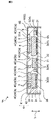
- FIG. 2 is a cross-sectional view showing the AA cross section in FIG. 1
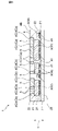
- FIG. 5 is a sectional view showing a BB section in FIG. 4;
- the top view of the electronic circuit module which concerns on 3rd Embodiment of this invention.
- FIG. 2 is a sectional view corresponding to the AA section of FIG. 1 in a modification of the electronic circuit module according to the first embodiment of the present invention
- FIG. 5 is a sectional view corresponding to the BB section of FIG. 4 in a modification of the electronic circuit module according to the second embodiment of the present invention;
- An electronic circuit module comprises: a substrate; at least one electronic component mounted on the main surface of the substrate; a sealing resin that has a lower surface that contacts the main surface of the substrate and an upper surface that is located on the opposite side of the substrate with respect to the electronic component and faces opposite to the lower surface, and that covers the electronic component; , An identification recess that constitutes at least one of an identification character and an identification mark when viewed from the thickness direction of the substrate is formed on the upper surface of the sealing resin, The identification recess is filled with a filler made of a material having a higher thermal conductivity than the sealing resin.
- the filler filled in the identification recess is made of a material with a higher thermal conductivity than the sealing resin. Therefore, the heat generated by the electronic component can be dissipated by the filler.
- the identification recess formed in the sealing resin is filled with a filler for dissipating heat generated by the electronic component. Therefore, the heat generated by the electronic component can be dissipated without additionally arranging a plate, film, or the like for dissipating the heat generated by the electronic component so as to overlap the sealing resin. As a result, it is possible to suppress an increase in the thickness of the electronic circuit module.
- the identification concave portion forming at least one of the identification characters and the identification mark when viewed from the thickness direction of the substrate is filled with the filler. Therefore, the filler constitutes at least one of the identification characters and the identification mark when viewed from the thickness direction of the substrate. That is, the filler for dissipating heat generated by the electronic component can function as at least one of the identification characters and the identification mark.
- the filler is made of a material different from the sealing resin. Therefore, the color of the filler and the reflection of light on the top surface of the filler are different from the color of the sealing resin and the reflection of light on the top surface of the sealing resin. Therefore, the visibility and identifiability of the identification characters and identification marks formed by the filler are improved over those of the identification characters and identification marks formed only by the steps of the concave portions formed in the sealing resin. be able to.
- the electronic component may include a heat-generating component, At least a portion of the filler may overlap at least a portion of the heat-generating component when viewed from the thickness direction.
- the sealing resin may be interposed between the filler and the heat-generating component.
- the sealing resin is interposed between the filler and the heat-generating component. Therefore, it is possible to prevent a short circuit as described above.
- the heat-generating component may be exposed in the identification recess,
- the filler may be in contact with the heat-generating component.
- the heat-generating component is a first part; a second part that is shorter in the thickness direction than the first part,
- the identification recess is a first recess;
- a second recess deeper in the thickness direction than the first recess may be provided, When viewed from the thickness direction, at least a portion of the filler filled in the first recess may overlap at least a portion of the first component, At least a portion of the filler filled in the second recess may overlap at least a portion of the second component when viewed from the thickness direction.
- the identification recess can have a depth corresponding to the height of the heat-generating component overlapping the identification recess when viewed from the thickness direction.
- the distance in the thickness direction of the substrate between the filler and the heat-generating component can be shortened. Therefore, it is possible to improve the heat radiation performance of the heat generated by the heat-generating component.
- the identification recesses located at positions overlapping with the low-height heat-generating components when viewed in the thickness direction are deep, the amount of filling material to be filled in the identification recesses increases. As a result, it is possible to improve the heat radiation performance of the heat generated by the low-height heat-generating component.
- An electronic circuit module comprises: A conductive shield film may be further provided that covers at least a region of the upper surface of the sealing resin in which the identification recess is formed.
- the heat generated by the heat-generating component can be dissipated not only by the filler but also by the shield film.
- a filling recess filled with the filling material may be further formed in a portion of the upper surface of the sealing resin where the identification recess is not formed.
- the heat generated by the heat-generating component can be dissipated not only by the filling material filled in the identification recess, but also by the filling material filled in the filling recess.
- FIG. 1 is a plan view of an electronic circuit module according to a first embodiment of the invention.
- FIG. 2 is a plan view of the electronic circuit module of FIG. 1 with the sealing resin removed.
- FIG. 3 is a cross-sectional view showing the AA cross section in FIG.
- the electronic circuit module 1 includes a substrate 2, electronic components 3, and a sealing resin 4. 2, illustration of the sealing resin 4 is omitted.
- the substrate 2 has an upper surface 2A and a lower surface 2B that is the back surface of the upper surface 2A.
- the upper surface 2A is an example of a main surface.
- the substrate 2 may be a single-layer substrate, a double-sided substrate, or a multilayer substrate.
- the substrate 2 is made of, for example, glass epoxy resin, low-temperature co-fired ceramic, or high-temperature co-fired ceramic.
- a mounting electrode 21 is provided on the upper surface 2A of the substrate 2.
- the mounting electrode 21 is made of a conductive material such as copper (Cu), silver (Ag), aluminum (Al), or a compound of these metals.
- the mounting electrodes 21 may be plated with nickel (Ni)/gold (Au).
- the electronic component 3 is mounted on the upper surface 2A of the substrate 2.
- Electronic component 3 is electrically connected to mounting electrodes 21 via solder bumps 22 .
- the electronic circuit module 1 includes 31 electronic components 3 in the first embodiment. That is, 31 electronic components 3 are mounted on the upper surface 2A of the substrate 2 in the first embodiment.
- the number of electronic components 3 included in the electronic circuit module 1 is not limited to 31 pieces.
- the electronic circuit module 1 may include only one electronic component 3 or may include 40 electronic components 3 . In other words, the electronic circuit module 1 only has to include at least one electronic component 3 .
- the electronic components 3 are, for example, semiconductor elements such as resistors, capacitors, inductors, filters, integrated circuits, and power amplifiers.
- the filters are, for example, surface acoustic wave filters, bulk acoustic wave filters, ceramic LC filters, and the like. In the first embodiment, a plurality of types of electronic components 3 are provided.
- the plurality of electronic components 3 include heat generating components.
- three electronic components 3 out of 31 electronic components 3 are heat-generating components 31 , 32 , 33 .
- Heat-generating components 31 , 32 , 33 generate more heat than other electronic components 3 mounted on upper surface 2 ⁇ /b>A of substrate 2 .
- the heat-generating components 31, 32, 33 are, for example, power amplifiers (PA), low-noise amplifiers (LNA), filters, and the like.
- the mounting height of the heat generating component 32 is lower than the mounting height of the heat generating component 31, as shown in FIG. In other words, the heat-generating component 32 is shorter in the thickness direction Y of the substrate 2 than the heat-generating component 31 .
- the heat-generating component 31 is an example of a first component.
- the heat-generating component 32 is an example of a second component.
- the sealing resin 4 is provided on the upper surface 2A of the substrate 2.
- the sealing resin 4 is composed of, for example, an epoxy resin or the like.
- the sealing resin 4 may contain a filler such as silica filler or alumina, for example.
- the sealing resin 4 covers the electronic components 3 mounted on the upper surface 2A of the substrate 2. In other words, the electronic component 3 is embedded within the sealing resin 4 .
- the sealing resin 4 has a lower surface 4A and an upper surface 4B.
- the bottom surface 4A contacts the top surface 2A of the substrate 2 .
- the upper surface 4B is located on the opposite side of the substrate 2 with respect to the electronic component 3 .
- the upper surface 4B faces away from the lower surface 4A.
- an upper surface 4B of the sealing resin 4 is formed with three recesses 4C (recesses 4Ca, 4Cb, 4Cc).
- recesses 4Ca, 4Cb, and 4Cc are collectively referred to as recess 4C.
- Each recess 4 ⁇ /b>C constitutes either one of an identification character and an identification mark when viewed from the thickness direction Y of the substrate 2 .
- Identification characters are, for example, hiragana, kanji, alphabets, or a combination thereof.
- Identification marks are, for example, numbers, symbols, dot-like recognition codes, bar codes, two-dimensional codes, logos, figures, or combinations thereof.
- the concave portion 4Cb formed in the shape of "MRT" constitutes the identification character.
- the recess 4Cb formed in the shape of a two-dimensional code and the recess 4Cc formed in the shape of a rectangle respectively constitute identification marks.
- the rectangular shape of the concave portion 4Cc described above functions as a direction mark formed to prevent the electronic circuit module 1 from being placed in the wrong direction.
- the recess 4C is an example of an identification recess.
- the recess 4Cb is deeper in the thickness direction Y of the substrate 2 than the recess 4Ca.
- the recess 4Ca is an example of a first recess.
- the recess 4Cb is an example of a second recess.
- the depth of the concave portion 4Cc may be the same as that of the concave portion 4Ca, the same as that of the concave portion 4Cb, or a depth different from that of both the concave portions 4Ca and 4Cb.
- the recess 4C does not reach the electronic component 3 located directly below the recess 4C.
- the depth of the recess 4C is shallower than the distance in the thickness direction Y of the substrate 2 between the electronic component 3 positioned directly below the recess 4C and the upper surface 4B of the sealing resin 4 .
- the depth of the recess 4Ca is 20-30 ⁇ m, and the depth of the recess 4Cb is 40-50 ⁇ m.
- the depth of the recess 4C is not limited to the depth described above.
- the concave portion 4C overlaps the heat-generating components 31, 32, and 33 when viewed from the thickness direction Y of the substrate 2.
- a portion of the concave portion 4Ca overlaps a portion of the heat-generating component 31 when viewed from the thickness direction Y of the substrate 2 .
- a portion of the recess 4Cb overlaps a portion of the heat-generating component 32.
- a portion of the recess 4Cc overlaps with the entire heat-generating component 33 (see FIG. 2).
- the manner in which the concave portion 4C and the heat-generating components 31, 32, and 33 overlap when viewed from the thickness direction Y of the substrate 2 is not limited to the manner described above.
- at least a portion of the recess 4C should overlap at least a portion of the heat-generating components 31, 32, and 33 when viewed from the thickness direction Y of the substrate 2.
- FIG. at least a portion of the recess 4Ca may overlap at least a portion of the heat-generating component 31 when viewed from the thickness direction Y of the substrate 2 .
- the concave portion 4Ca may overlap both a portion of the heat-generating component 31 and a portion of the heat-generating component 32 when viewed from the thickness direction Y of the substrate 2 . Further, for example, each of the concave portions 4Ca and 4Cb may overlap the heat-generating component 31 when viewed from the thickness direction Y of the substrate 2 .
- the recess 4C is formed by removing the sealing resin 4 with, for example, a laser.
- the recess 4C is filled with the filler 5.
- the filler 5 is made of a material having higher thermal conductivity than the sealing resin 4 .
- the filler 5 is composed of silver.
- the filling material 5 is filled into the recesses 4C by pouring the silver paste into the recesses 4C.
- the filler 5 is not limited to silver.
- the filler 5 may be copper, aluminum, or the like. Further, for example, the filler 5 may be a resin containing a metal material.
- the recess 4C does not reach the electronic component 3 located directly below the recess 4C. That is, the sealing resin 4 is interposed between the filling material 5 filled in the recess 4C and the electronic component 3 overlapping the recess 4C when viewed from the thickness direction Y of the substrate 2 .
- the sealing resin 4 is interposed between the heat-generating component 31 and the filler 5 filled in the recess 4Ca. Also, the sealing resin 4 is interposed between the filler 5 filled in the concave portion 4Cb and the heat-generating component 32 .
- the sealing resin 4 is interposed between the filler 5 filled in the recess 4Cc and the heat-generating component 33 (see FIG. 2).
- the recess 4C overlaps the heat-generating components 31, 32, and 33. That is, when viewed from the thickness direction Y of the substrate 2 , the filler 5 filled in the recess 4 ⁇ /b>C overlaps the heat-generating components 31 , 32 , 33 .
- a portion of the filler 5 filled in the concave portion 4Ca overlaps a portion of the heat-generating component 31. As shown in FIG.
- a portion of the filler 5 filled in the concave portion 4 ⁇ /b>Cb overlaps a portion of the heat-generating component 32 .
- a portion of the filler 5 filled in the recess 4Cc overlaps with the entire heat-generating component 33 (see FIG. 2).
- the manner in which the concave portion 4C and the heat-generating components 31, 32, and 33 overlap when viewed from the thickness direction Y of the substrate 2 is not limited to the manner shown in FIGS. Therefore, when viewed from the thickness direction Y of the substrate 2, the manner in which the filling material 5 filled in the recess 4C and the heat-generating components 31, 32, and 33 are overlapped is not limited to the manner described above. In other words, at least a portion of the filler 5 filled in the recess 4C should overlap at least a portion of the heat-generating components 31, 32, and 33 when viewed from the thickness direction Y of the substrate 2.
- the entirety of the filling material 5 filled in the concave portion 4Cc may overlap a portion of the heat-generating component 33 when viewed from the thickness direction Y of the substrate 2 .
- the outer edge of the recess 4Cc and the outer surface of the heat-generating component 33 may match.
- the entirety of the filler 5 filled in the concave portion 4 ⁇ /b>Cc overlaps the entirety of the heat-generating component 33 .
- At least a portion of the filler 5 filled in the concave portion 4Ca may overlap at least a portion of the heat-generating component 31 when viewed from the thickness direction Y of the substrate 2 .
- the filling material 5 filled in the concave portion 4Ca may overlap both a portion of the heat generating component 31 and a portion of the heat generating component 32 .
- the filling material 5 filled in the recess 4Ca and the filling material 5 filled in the recess 4Cb may each overlap the heat-generating component 31 .
- the color and brightness of the filler 5 can be different from the color and brightness of the sealing resin 4 .
- the color of one of the filler 5 and the encapsulating resin 4 can be complementary to the other of the filler 5 and the encapsulating resin 4 .
- one of the filler 5 and the sealing resin 4 may be bright and the other of the filler 5 and the sealing resin 4 may be dark. As a result, the identifiability and visibility of the identification characters and identification marks formed by the filler 5 can be enhanced.
- the filler 5 is white-based
- the sealing resin 4 is black-based.
- the filler 5 filled in the recess 4C is made of a material having a higher thermal conductivity than the sealing resin 4. Therefore, the heat generated by the electronic component 3 can be dissipated by the filler 5 .
- the recess 4C formed in the sealing resin 4 is filled with the filler 5 for dissipating heat generated by the electronic component 3 . Therefore, the heat generated by the electronic component 3 can be dissipated without additionally arranging a plate, film, or the like for dissipating the heat generated by the electronic component 3 so as to overlap the sealing resin 4 . As a result, an increase in the thickness of the electronic circuit module 1 can be suppressed.
- the filling material 5 is filled in the concave portion 4C forming at least one of the identification characters and the identification mark when viewed from the thickness direction Y of the substrate 2 .
- the filler 5 constitutes at least one of the identification characters and the identification mark when viewed from the thickness direction Y of the substrate 2 .
- the filler 5 for dissipating the heat generated by the electronic component 3 can function as at least one of the identification characters and the identification mark.
- the filler 5 is made of a material different from the sealing resin 4. Therefore, the color of the filler 5 and the reflection of light on the top surface of the filler 5 are different from the color of the sealing resin 4 and the reflection of light on the top surface 4B of the sealing resin 4 . Therefore, the visibility and identifiability of the identification characters and identification marks formed by the filler 5 are compared with the visibility and identifiability of the identification characters and identification marks formed only by the steps of the recesses formed in the sealing resin 4. can be improved.
- the filler 5 since the filler 5 does not overlap the heat-generating components 31, 32, 33 when viewed from the thickness direction Y of the substrate 2, the heat generated by the heat-generating components 31, 32, 33 is reduced by the filler 5. Heat dissipation can be improved.
- the sealing resin 4 is interposed between the filler 5 and the heat generating components 31 , 32 , 33 . Therefore, it is possible to prevent a short circuit as described above.
- the depth of each of the recesses 4Ca, 4Cb, and 4Cc is the height of the heat-generating components 31, 32, and 33 overlapping each of the recesses 4Ca, 4Cb, and 4Cc when viewed from the thickness direction Y of the substrate 2.
- the depth can be set according to In the first embodiment, the recess 4Cb located directly above the heat-generating component 32 whose mounting height is lower than the heat-generating component 31 is deeper than the recess 4Ca located directly above the heat-generating component 31 .
- the distance in the thickness direction Y of the substrate 2 between the filler 5 filled in the recess 4Cb and the heat-generating component 32 can be shortened.
- the heat radiation property of the heat generated by the heat generating component 32 can be improved.
- the depth of the recess 4Cb at the position overlapping with the low-height heat-generating component 32 when viewed from the thickness direction Y of the substrate 2 increases the amount of the filling material 5 filled in the recess 4Cb. Thereby, the heat radiation property of the heat generated by the heat-generating component 32 can be improved.
- external electrodes may be provided on the bottom surface 2B of the substrate 2 .
- the electronic circuit module 1 is mounted, for example, on a mother board via external electrodes.
- the external electrodes may be electrically connected to the mounting electrodes 21 .
- power is supplied to the electronic component 3 and signals are transmitted through the external electrodes.
- the external electrodes may be connected to an external ground potential (for example, the ground potential of the motherboard). In this case, the electronic component 3 can be grounded.
- internal electrodes may be provided inside the substrate 2 .
- the external electrodes and the internal electrodes may be plated in the same manner as the mounting electrodes 21 .
- the electronic component 3 may be mounted on the bottom surface 2B of the substrate 2 instead of the top surface 2A of the substrate 2.
- the lower surface 2B corresponds to the main surface.
- the electronic components 3 may be mounted on both the top surface 2A and the bottom surface 2B of the board 2 .
- the upper surface 2A and the lower surface 2B correspond to main surfaces.
- the sealing resin 4 may be provided on the lower surface 2B of the substrate 2, or may be provided on both the upper surface 2A and the lower surface 2B of the substrate 2.
- the recess 4C may be formed in the sealing resin 4 provided on the bottom surface 2B of the substrate 2.
- the filling material 5 may be filled in the concave portion 4C formed in the sealing resin 4 provided on the lower surface 2B of the substrate 2 .
- the electronic circuit module 1 has three recesses 4C in the first embodiment, the electronic circuit module 1 may have at least one recess 4C.
- the recess 4Cb constitutes the identification character
- the recesses 4Ca, 4Cc constitute the identification mark
- the present invention is not limited to this.
- all of the concave portions 4Ca, 4Cb and 4Cc may constitute identification characters, or all of the concave portions 4Ca, 4Cb and 4Cc may constitute identification marks.
- the concave portion 4Cb may constitute the identification mark
- the concave portions 4Ca and 4Cc may constitute the identification characters.
- each of the three recesses 4Ca, 4Cb, 4Cc is composed of only one of the identification characters and the identification mark.
- one recess 4C for example recess 4Ca, may contain both identification characters and identification marks. That is, at least one of the identification character and the identification mark is configured by one concave portion 4C.
- FIG. 8 is a sectional view corresponding to the AA section of FIG. 1 in the modification of the electronic circuit module according to the first embodiment of the present invention.
- the sealing resin 4 is interposed between the recess 4C and the electronic component 3 when viewed from the thickness direction Y of the substrate 2 .
- the sealing resin 4 does not have to be interposed between the recess 4C and the electronic component 3 when viewed from the thickness direction Y of the substrate 2 . That is, the recess 4 ⁇ /b>C may reach the electronic component 3 by passing through the sealing resin 4 in the thickness direction Y of the substrate 2 .
- the electronic component 3 may be exposed in the recess 4C.
- the filling material 5 filled in the recess 4 ⁇ /b>C contacts the electronic component 3 .
- the sealing resin 4 is not interposed between the recess 4C and the heat-generating components 31,32. Also, although not shown, the sealing resin 4 is not interposed between the recess 4C and the heat-generating component 33 either. That is, the filler 5 filled in the recess 4C contacts all the heat-generating components 31, 32, 33. As shown in FIG. However, the filler 5 may be in contact with only some of the heat generating components 31, 32, 33. For example, the filler 5 may be in contact with the heat-generating component 31 but not in contact with the heat-generating components 32 and 33 .
- the heat-generating component 32 is shorter in the thickness direction Y of the substrate 2 than the heat-generating component 31 .
- the height of each of the electronic components 3 including the heat generating components 31 and 32 is not limited to the height shown in FIG. 3 and the like.
- heat-generating component 31 may be the same height as heat-generating component 32 .
- the recess 4Cb is deeper in the thickness direction Y of the substrate 2 than the recess 4Ca.
- the depth of each of the recesses 4Ca, 4Cb, 4Cc is not limited to the depth described above.
- the recesses 4Ca, 4Cb, 4Cc may have the same depth.
- FIG. 4 is a plan view of an electronic circuit module according to a second embodiment of the invention.
- FIG. 5 is a sectional view showing a BB section in FIG.
- the electronic circuit module 1A according to the second embodiment differs from the electronic circuit module 1 according to the first embodiment in that the electronic circuit module 1A according to the second embodiment includes a shield film 6.
- FIG. Differences from the first embodiment will be described below. Points in common with the electronic circuit module 1 of the first embodiment are denoted by the same reference numerals, and descriptions thereof are omitted in principle, and will be described as necessary. This also applies to each embodiment described later.
- the shield film 6 covers the upper and lateral sides of the substrate 2 and the sealing resin 4 .
- the shield film 6 has conductivity. Typically, at least part of shield film 6 is made of metal.
- the shield film 6 is made of a conductive member such as copper. A portion of the shield film 6 may be made of a conductive member.
- the shield film 6 may be one in which a conductive material is contained in another material such as resin.
- FIG. 9 is a sectional view corresponding to the BB section of FIG. 4 in a modification of the electronic circuit module according to the second embodiment of the present invention.
- the shield film 6 is formed by sputtering or vapor deposition, for example.
- the film thickness of the shield film 6 is, for example, 2 ⁇ m or more and less than 5 ⁇ m.
- the shield film 6 may have a multilayer structure.
- the shield film 6 includes an adhesion layer in contact with the sealing resin 4, a conductive layer in contact with the adhesion layer and made of a metal with high conductivity, and a conductive layer in contact with the conductive layer by oxidation or oxidation of the conductive layer. It may also have an antirust layer that prevents corrosion.
- the conductive layer has a function of shielding electromagnetic waves, and is made of, for example, copper (Cu), silver (Ag), aluminum (Al), or the like.
- the adhesion layer is provided to enhance adhesion between the sealing resin 4 and the conductive layer, and is made of, for example, titanium (Ti), chromium (Cr), stainless steel (SUS), or the like.
- the shield film 6 shields electromagnetic waves from the outside of the electronic circuit module 1 . Therefore, the electronic component 3 is less likely to be affected by electromagnetic waves from the outside. Also, the shield film 6 shields electromagnetic waves radiated by the electronic component 3 . Therefore, the electromagnetic waves radiated from the electronic component 3 are less likely to affect other components outside the electronic circuit module 1 .
- the shield film 6 radiates the heat generated by the heat-generating components 31 , 32 , 33 .
- the shield film 6 may be connected to an external ground potential (for example, the ground potential of the mother substrate).
- the shield film 60 includes an upper film 61 and side films 62 .
- the upper film 61 is laminated on the upper surface 4B of the sealing resin 4 .
- the side film 62 extends from the peripheral edge of the top film 61 .
- the side film 62 is laminated on side surfaces of the sealing resin 4 and the substrate 2 .
- the upper film 61 is in contact with the filling material 5 filled in the recess 4C from above.
- the filler 5 is thereby electrically connected to the shield film 6 .
- the filler 5 can be grounded through the shield film 6 .
- the mounting electrode 21 may be electrically connected to the shield film 6 .
- the mounting electrode 21 can be grounded via the shield film 6 .
- the electronic circuit module 1A includes external electrodes and internal electrodes, the external electrodes and the internal electrodes may be electrically connected to the shield film 6 .
- the filler 5 is covered with the shield film 6 from above. Therefore, the filler 5 cannot be visually recognized directly. However, it is possible to recognize the identification characters and identification marks constituted by the filler material 5, as explained below.
- the filler 5 and the sealing resin 4 are made of different materials. Therefore, the configuration of the upper surface 4B of the sealing resin 4 is different from the configuration of the upper surface of the filler 5. As shown in FIG. For example, while the upper surface 4B of the sealing resin 4 has many irregularities, the filler 5 made of silver, that is, the upper surface of the filler 5 made of metal is more uneven than the upper surface 4B of the sealing resin 4. nearly smooth. In this case, after the recess 4C is filled with the filler 5, the sealing resin 4 is polished together with the filler 5 so that the upper surface 4B of the sealing resin 4 and the upper surface of the filler 5 are flush with each other. However, the above-described difference in surface configuration occurs.
- the portion of the upper film 61 of the shield film 6 that contacts the sealing resin 4 and the upper surface of the shield film 6 The structure of the upper surface 61A (see FIG. 5) of the upper film 61 is different from that of the film 61 which is in contact with the filling material 5 .
- the light penetrates the filling material 5 of the upper film 61 in the region of the upper film 61 that contacts the upper surface 4B of the sealing resin 4 . It reflects differently than the area that touches the top surface.
- the identification characters and identification marks formed by the filler 5 can be visually recognized and identified through the upper film 61 .
- the identification characters and identification marks formed by the filler 5 can be visually recognized and identified even by the step. can do.
- the heat generated by the heat-generating components 31, 32, and 33 can be radiated not only by the filler 5 but also by the shield film 6.
- the shield film 6 is provided so as to cover the top and sides of the substrate 2 and the sealing resin 4, but it is not limited to this.
- the shield film 6 only needs to cover at least the region of the upper surface 4B of the sealing resin 4 where the recess 4C is formed.
- the shield film 6 may be composed of only the upper film 61 without the side film 62 .
- FIG. 6 is a plan view of an electronic circuit module 1B according to the third embodiment of the invention.
- the electronic circuit module 1B according to the third embodiment differs from the electronic circuit module 1 according to the first embodiment in that the electronic circuit module 1B according to the third embodiment has a concave portion 4D. Differences from the first embodiment will be described below.
- the upper surface 4B of the sealing resin 4 is formed with one recess 4D in addition to the three recesses 4C.
- the recess 4D is filled with the filler 5 in the same manner as the recess 4C.
- the recess 4D is an example of a filling recess.
- the recess 4D is formed in a region of the upper surface 4B of the sealing resin 4 where the recess 4C is not formed.
- the recess 4D when viewed from the thickness direction Y of the substrate 2, does not overlap the heat-generating components 31, 32, 33, but overlaps some of the electronic components 3 other than the heat-generating components 31, 32, 33. ing. However, at least a portion of the recess 4 ⁇ /b>D may overlap at least a portion of the heat-generating components 31 , 32 , 33 when viewed from the thickness direction Y of the substrate 2 . Moreover, when viewed from the thickness direction Y of the substrate 2, the recess 4D does not have to overlap the electronic components 3 other than the heat generating components 31, 32, and 33.
- the recess 4D and the filling material 5 filled in the recess 4D constitute neither identification characters nor identification marks.
- the recess 4D and the filler 5 filled in the recess 4D may constitute at least one of the identification characters and the identification mark.
- the recess 4D corresponds to an identification recess that does not overlap the heat-generating components 31, 32, and 33 when viewed from the thickness direction Y of the substrate 2.
- the electronic circuit module 1B has one recess 4D.
- the recesses 4D may be formed at a plurality of locations on the upper surface 4B of the sealing resin 4.
- the depth of the recess 4D may be deeper than the recess 4C, may be shallower than the recess 4C, or may be the same as the recess 4C.
- the heat generated by the heat-generating components 31, 32, and 33 can be dissipated not only by the filler 5 filled in the recess 4C but also by the filler 5 filled in the recess 4D.
- FIG. 7 is a plan view of an electronic circuit module 1C according to a fourth embodiment of the invention.
- the electronic circuit module 1C according to the fourth embodiment differs from the electronic circuit module 1B according to the third embodiment in that the electronic circuit module 1C according to the fourth embodiment includes a shield film 6.
- FIG. Differences from the third embodiment will be described below.
- the difference between the electronic circuit module 1C according to the fourth embodiment and the electronic circuit module 1B according to the third embodiment is that the electronic circuit module 1A according to the second embodiment differs from the electronic circuit module 1 according to the first embodiment. is similar to In other words, the electronic circuit module 1C is obtained by adding the shield film 6 having the same configuration as that of the electronic circuit module 1A to the electronic circuit module 1B. In other words, the electronic circuit module 1C is obtained by covering the substrate 2 and the sealing resin 4 of the electronic circuit module 1B above and laterally with the shield film 6 .
- the heat generated by the heat-generating components 31, 32, and 33 can be radiated not only by the filler 5 but also by the shield film 6.
Landscapes
- Engineering & Computer Science (AREA)
- Microelectronics & Electronic Packaging (AREA)
- Structures Or Materials For Encapsulating Or Coating Semiconductor Devices Or Solid State Devices (AREA)
Abstract
厚みの増加を抑制しつつ、電子部品が発する熱を放熱することができ、識別文字及び識別マークの識別性及び視認性を従来技術より向上することができる電子回路モジュールを提供する。本発明に係る電子回路モジュール1は、基板2と、基板2の上面2Aに実装される複数の電子部品3と、電子部品3を覆う封止樹脂4とを備える。封止樹脂4は、基板2の上面2Aに接触する下面4Aと、電子部品3に対して基板2の反対側に位置して下面4Aと反対を向く上面4Bとを有する。封止樹脂4の上面4Bに、基板2の厚み方向Yから見て識別文字及び識別マークの少なくとも一方を構成する凹部4Cが形成される。凹部4Cに、封止樹脂4より熱伝導率が高い材料からなる充填材5が充填されている。
Description
本発明は、基板と、基板に実装される電子部品とを備える電子回路モジュールに関する。
識別文字及び識別マークの少なくとも一方を有する電子回路モジュールが知られている。例えば、特許文献1に開示される半導体装置では、放熱グリスを介して半導体素子に接合されたアルミニウム板が切削されることによって、マークが形成される。
電子回路モジュールでは、電子部品が発する熱を放熱することが求められる。例えば、特許文献1に開示される半導体装置では、半導体素子が発する熱は放熱グリス及びアルミニウム板によって放熱される。
特許文献1に開示される半導体装置では、マークは、アルミニウム板の凹凸のみによって形成される。そのため、マークの識別性及び視認性が十分に得られないおそれがある。
また、特許文献1に開示される半導体装置では、放熱グリスに加えてアルミニウム板が重ねられる。そのため、半導体装置の厚みが増してしまう。
従って、本発明の目的は、前記課題を解決することにあって、厚みの増加を抑制しつつ、電子部品が発する熱を放熱することができ、識別文字及び識別マークの識別性及び視認性を従来技術より向上することができる電子回路モジュールを提供することにある。
前記目的を達成するために、本発明は以下のように構成する。
本発明の一態様に係る電子回路モジュールは、
基板と、
前記基板の主面に実装される少なくとも1個の電子部品と、
前記基板の主面に接触する下面と、前記電子部品に対して前記基板の反対側に位置して前記下面と反対を向く上面とを有し、前記電子部品を覆う封止樹脂と、を備え、
前記封止樹脂の上面に、前記基板の厚み方向から見て識別文字及び識別マークの少なくとも一方を構成する識別凹部が形成され、
前記識別凹部に、前記封止樹脂より熱伝導率が高い材料からなる充填材が充填されている。
本発明の一態様に係る電子回路モジュールは、
基板と、
前記基板の主面に実装される少なくとも1個の電子部品と、
前記基板の主面に接触する下面と、前記電子部品に対して前記基板の反対側に位置して前記下面と反対を向く上面とを有し、前記電子部品を覆う封止樹脂と、を備え、
前記封止樹脂の上面に、前記基板の厚み方向から見て識別文字及び識別マークの少なくとも一方を構成する識別凹部が形成され、
前記識別凹部に、前記封止樹脂より熱伝導率が高い材料からなる充填材が充填されている。
本発明によれば、厚みの増加を抑制しつつ、電子部品が発する熱を放熱することができ、識別文字及び識別マークの識別性及び視認性を従来技術より向上することができる。
本発明の一態様に係る電子回路モジュールは、
基板と、
前記基板の主面に実装される少なくとも1個の電子部品と、
前記基板の主面に接触する下面と、前記電子部品に対して前記基板の反対側に位置して前記下面と反対を向く上面とを有し、前記電子部品を覆う封止樹脂と、を備え、
前記封止樹脂の上面に、前記基板の厚み方向から見て識別文字及び識別マークの少なくとも一方を構成する識別凹部が形成され、
前記識別凹部に、前記封止樹脂より熱伝導率が高い材料からなる充填材が充填されている。
基板と、
前記基板の主面に実装される少なくとも1個の電子部品と、
前記基板の主面に接触する下面と、前記電子部品に対して前記基板の反対側に位置して前記下面と反対を向く上面とを有し、前記電子部品を覆う封止樹脂と、を備え、
前記封止樹脂の上面に、前記基板の厚み方向から見て識別文字及び識別マークの少なくとも一方を構成する識別凹部が形成され、
前記識別凹部に、前記封止樹脂より熱伝導率が高い材料からなる充填材が充填されている。
この構成によれば、識別凹部に充填された充填材は、封止樹脂より熱伝導率が高い材料からなる。そのため、電子部品が発する熱を充填材によって放熱することができる。
この構成によれば、電子部品が発する熱を放熱するための充填材が、封止樹脂に形成された識別凹部に充填される。そのため、電子部品が発する熱を放熱するための板及び膜等を封止樹脂に重ねて追加配置することなく、電子部品が発する熱を放熱することができる。その結果、電子回路モジュールの厚みが増加することを抑制することができる。
この構成によれば、基板の厚み方向から見て識別文字及び識別マークの少なくとも一方を構成する識別凹部に、充填材が充填されている。そのため、充填材は、基板の厚み方向から見て識別文字及び識別マークの少なくとも一方を構成する。つまり、電子部品が発する熱を放熱するための充填材を、識別文字及び識別マークの少なくとも一方として機能させることができる。
充填材は、封止樹脂とは異なる材料からなる。そのため、充填材の色及び充填材の上面における光の反射は、封止樹脂の色及び封止樹脂の上面における光の反射と異なる。よって、充填材によって構成される識別文字及び識別マークの視認性及び識別性を、封止樹脂に形成された凹部の段差のみによって構成される識別文字及び識別マークの視認性及び識別性より向上することができる。
前記電子回路モジュールにおいて、
前記電子部品は、発熱部品を含んでもよく、
前記厚み方向から見て、前記充填材の少なくとも一部は、前記発熱部品の少なくとも一部と重なってもよい。
前記電子部品は、発熱部品を含んでもよく、
前記厚み方向から見て、前記充填材の少なくとも一部は、前記発熱部品の少なくとも一部と重なってもよい。
この構成によれば、厚み方向から見て充填材が発熱部品と重なっていない構成より、充填材による発熱部品が発する熱の放熱性を向上することができる。
前記電子回路モジュールにおいて、
前記充填材と前記発熱部品との間に、前記封止樹脂が介在してもよい。
前記充填材と前記発熱部品との間に、前記封止樹脂が介在してもよい。
仮に充填材が発熱部品と接触する場合、充填材と発熱部品の電極とが短絡するおそれがある。この構成によれば、充填材と発熱部品との間に、封止樹脂が介在する。そのため、前述したような短絡を防止することができる。
前記電子回路モジュールにおいて、
前記発熱部品は、前記識別凹部に露出していてもよく、
前記充填材は、前記発熱部品と接触していてもよい。
前記発熱部品は、前記識別凹部に露出していてもよく、
前記充填材は、前記発熱部品と接触していてもよい。
この構成によれば、充填材が発熱部品と接触していない構成より、充填材による発熱部品が発する熱の放熱性を向上することができる。
前記電子回路モジュールにおいて、
前記発熱部品は、
第1部品と、
前記第1部品より前記厚み方向に短い第2部品と、を備えてもよく、
前記識別凹部は、
第1凹部と、
前記第1凹部より前記厚み方向に深い第2凹部と、を備えてもよく、
前記厚み方向から見て、前記第1凹部に充填された前記充填材の少なくとも一部は、前記第1部品の少なくとも一部と重なってもよく、
前記厚み方向から見て、前記第2凹部に充填された前記充填材の少なくとも一部は、前記第2部品の少なくとも一部と重なってもよい。
前記発熱部品は、
第1部品と、
前記第1部品より前記厚み方向に短い第2部品と、を備えてもよく、
前記識別凹部は、
第1凹部と、
前記第1凹部より前記厚み方向に深い第2凹部と、を備えてもよく、
前記厚み方向から見て、前記第1凹部に充填された前記充填材の少なくとも一部は、前記第1部品の少なくとも一部と重なってもよく、
前記厚み方向から見て、前記第2凹部に充填された前記充填材の少なくとも一部は、前記第2部品の少なくとも一部と重なってもよい。
この構成によれば、識別凹部を、厚み方向から見て当該識別凹部と重なる発熱部品の高さに応じた深さとすることができる。これにより、充填材と発熱部品との基板の厚み方向の距離を短くすることできる。そのため、発熱部品が発する熱の放熱性を向上することができる。
この構成によれば、厚み方向から見て低い高さの発熱部品と重なる位置にある識別凹部が深いため、当該識別凹部に充填される充填材の量が増える。これにより、当該低い高さの発熱部品が発する熱の放熱性を向上することができる。
本発明の一態様に係る電子回路モジュールは、
前記封止樹脂の上面のうち、少なくとも前記識別凹部が形成された領域を覆う導電性のシールド膜を更に備えてもよい。
前記封止樹脂の上面のうち、少なくとも前記識別凹部が形成された領域を覆う導電性のシールド膜を更に備えてもよい。
この構成によれば、充填材に加えてシールド膜によっても、発熱部品が発する熱を放熱することができる。
前記電子回路モジュールにおいて、
前記封止樹脂の上面のうち、前記識別凹部が形成されていない領域の一部に、前記充填材が充填される充填凹部が更に形成されてもよい。
前記封止樹脂の上面のうち、前記識別凹部が形成されていない領域の一部に、前記充填材が充填される充填凹部が更に形成されてもよい。
この構成によれば、識別凹部に充填される充填材に加えて、充填凹部に充填される充填材によっても、発熱部品が発する熱を放熱することができる。
以下、本発明の実施形態について、図面を参照しながら説明する。なお、本発明は、以下の実施形態によって限定されるものではない。また、図面において実質的に同一の部材については、同一の符号を付すことにより説明を省略する。
以下では、説明の便宜上、「上面」、「下面」、「側面」等の方向を示す用語を用いるが、これらの用語は、本発明に係る電子回路モジュールの使用状態等を限定することを意味するものではない。
<第1実施形態>
図1は、本発明の第1実施形態に係る電子回路モジュールの平面図である。図2は、図1の電子回路モジュールから封止樹脂を除いた電子回路モジュールの平面図である。図3は、図1におけるA-A断面を示す断面図である。
図1は、本発明の第1実施形態に係る電子回路モジュールの平面図である。図2は、図1の電子回路モジュールから封止樹脂を除いた電子回路モジュールの平面図である。図3は、図1におけるA-A断面を示す断面図である。
図1~図3に示すように、電子回路モジュール1は、基板2と、電子部品3と、封止樹脂4とを備える。なお、図2において、封止樹脂4の図示は省略されている。
図3に示すように、基板2は、上面2Aと、上面2Aの裏面である下面2Bとを有する。上面2Aは、主面の一例である。基板2は、単層基板、両面基板、または多層基板のいずれでもよい。基板2は、例えば、ガラスエポキシ樹脂、低温同時焼成セラミック、または高温同時焼成セラミックなどで構成される。
基板2の上面2Aに、実装電極21が設けられている。実装電極21は、例えば、銅(Cu)、銀(Ag)、アルミニウム(Al)、またはこれらの金属の化合物などの導電材料で構成される。実装電極21には、ニッケル(Ni)/金(Au)めっきが施されてもよい。
電子部品3は、基板2の上面2Aに実装されている。電子部品3は、はんだバンプ22を介して実装電極21と電気的に接続されている。図2に示すように、第1実施形態において、電子回路モジュール1は、31個の電子部品3を備える。つまり、第1実施形態において、31個の電子部品3が、基板2の上面2Aに実装されている。なお、電子回路モジュール1が備える電子部品3の数は、31個に限らない。例えば、電子回路モジュール1は、1個のみの電子部品3を備えていてもよいし、40個の電子部品3を備えていてもよい。つまり、電子回路モジュール1は、少なくとも1個の電子部品3を備えていればよい。
電子部品3は、例えば、抵抗、コンデンサ、インダクタ、フィルタ、集積回路、パワーアンプなどの半導体素子などである。フィルタは、例えば、表面弾性波フィルタ、バルク弾性波フィルタ、セラミックLCフィルタ等である。第1実施形態では、複数の種類の電子部品3が設けられている。
複数の電子部品3は、発熱部品を含む。第1実施形態では、31個の電子部品3のうち、3個の電子部品3が発熱部品31,32,33である。発熱部品31,32,33は、基板2の上面2Aに実装された他の電子部品3より発熱量が大きい。発熱部品31,32,33は、例えば、パワーアンプ(PA)、ローノイズアンプ(LNA)、フィルタ等である。
第1実施形態において、図3に示すように、発熱部品32の実装高さは、発熱部品31の実装高さより低い。言い換えると、発熱部品32は、発熱部品31より基板2の厚み方向Yに短い。発熱部品31は、第1部品の一例である。発熱部品32は、第2部品の一例である。
封止樹脂4は、基板2の上面2Aに設けられている。封止樹脂4は、例えば、エポキシ樹脂等で構成される。封止樹脂4は、例えば、シリカフィラーやアルミナ等のフィラーを含有してもよい。
封止樹脂4は、基板2の上面2Aに実装された電子部品3を覆っている。言い換えると、電子部品3は、封止樹脂4内に埋設されている。封止樹脂4は、下面4Aと、上面4Bとを有する。下面4Aは、基板2の上面2Aに接触する。上面4Bは、電子部品3に対して基板2の反対側に位置している。上面4Bは、下面4Aと反対を向いている。
図1に示すように、封止樹脂4の上面4Bに、3つの凹部4C(凹部4Ca,4Cb,4Cc)が形成されている。以下の説明において、凹部4Ca,4Cb,4Ccは、凹部4Cと総称される。凹部4Cの各々は、基板2の厚み方向Yから見て、識別文字及び識別マークのいずれか一方を構成している。識別文字は、例えば、ひらがな、漢字、アルファベット、またはそれらの組み合わせである。識別マークは、例えば、数字、記号、ドット状の認識用コード、バーコード、2次元コード、ロゴ、図形、またはそれらの組合せである。
第1実施形態では、図1に示すように、「MRT」の形状に形成された凹部4Cbは、識別文字を構成する。また、二次元コードの形状に形成された凹部4Cbと、長方形の形状に形成された凹部4Ccとは、それぞれ識別マークを構成する。なお、前述した凹部4Ccの長方形の形状は、電子回路モジュール1を誤った向きに配置することを防止するため等に形成される方向マークとして機能する。凹部4Cは、識別凹部の一例である。
図3に示すように、凹部4Cbは、凹部4Caより基板2の厚み方向Yに深い。凹部4Caは、第1凹部の一例である。凹部4Cbは、第2凹部の一例である。なお、凹部4Ccの深さは、凹部4Caと同一でもよいし、凹部4Cbと同一でもよいし、凹部4Ca,4Cbのいずれとも異なる深さでもよい。
凹部4Cは、当該凹部4Cの真下に位置する電子部品3に到達していない。つまり、凹部4Cの深さは、当該凹部4Cの真下に位置する電子部品3と封止樹脂4の上面4Bとの基板2の厚み方向Yの距離より浅い。
第1実施形態において、凹部4Caの深さは、20~30μmであり、凹部4Cbの深さは、40~50μmである。凹部4Cの深さは、前述した深さに限らない。
図1に示すように、基板2の厚み方向Yから見て、凹部4Cは、発熱部品31,32,33と重なっている。第1実施形態において、基板2の厚み方向Yから見て、凹部4Caの一部は、発熱部品31の一部と重なっている。また、基板2の厚み方向Yから見て、凹部4Cbの一部は、発熱部品32の一部と重なっている。また、基板2の厚み方向Yから見て、凹部4Ccの一部は、発熱部品33(図2参照)の全部と重なっている。
なお、基板2の厚み方向Yから見たときの、凹部4Cと発熱部品31,32,33との重なりの態様は、前述した態様に限らない。つまり、基板2の厚み方向Yから見て、凹部4Cの少なくとも一部が、発熱部品31,32,33の少なくとも一部と重なっていればよい。例えば、基板2の厚み方向Yから見て、凹部4Caの少なくとも一部が、発熱部品31の少なくとも一部と重なっていてもよい。また、例えば、基板2の厚み方向Yから見て、凹部4Caが、発熱部品31の一部及び発熱部品32の一部の双方と重なっていてもよい。また、例えば、基板2の厚み方向Yから見て、凹部4Ca,4Cbの各々が、発熱部品31と重なっていてもよい。
凹部4Cは、例えば、レーザーによって、封止樹脂4を除去することにより形成される。
図1及び図3に示すように、凹部4Cに、充填材5が充填されている。充填材5は、封止樹脂4より熱伝導性が高い材料からなる。第1実施形態において、充填材5は、銀で構成されている。銀ペーストが凹部4Cに流し込まれることによって、充填材5が凹部4Cに充填される。充填材5は、銀に限らない。例えば、充填材5は、銅、アルミニウム等であってもよい。また、例えば、充填材5は、金属材料を含む樹脂であってもよい。
前述したように、凹部4Cは、当該凹部4Cの真下に位置する電子部品3に到達していない。つまり、凹部4Cに充填された充填材5と、基板2の厚み方向Yから見て凹部4Cと重なる電子部品3との間に、封止樹脂4が介在している。第1実施形態では、図3に示すように、凹部4Caに充填された充填材5と、発熱部品31との間に封止樹脂4が介在している。また、凹部4Cbに充填された充填材5と、発熱部品32との間に封止樹脂4が介在している。また、図示されていないが、凹部4Ccに充填された充填材5と、発熱部品33(図2参照)との間に封止樹脂4が介在している。
前述したように、基板2の厚み方向Yから見て、凹部4Cは、発熱部品31,32,33と重なっている。つまり、基板2の厚み方向Yから見て、凹部4Cに充填された充填材5は、発熱部品31,32,33と重なっている。第1実施形態では、基板2の厚み方向Yから見て、凹部4Caに充填された充填材5の一部は、発熱部品31の一部と重なっている。また、基板2の厚み方向Yから見て、凹部4Cbに充填された充填材5の一部は、発熱部品32の一部と重なっている。また、基板2の厚み方向Yから見て、凹部4Ccに充填された充填材5の一部は、発熱部品33(図2参照)の全部と重なっている。
なお、前述したように、基板2の厚み方向Yから見た場合の、凹部4Cと発熱部品31,32,33との重なりの態様は、図1~図3に示すような態様に限らない。そのため、基板2の厚み方向Yから見た場合の、凹部4Cに充填された充填材5と発熱部品31,32,33との重なりの態様も、前述した態様に限らない。つまり、基板2の厚み方向Yから見て、凹部4Cに充填された充填材5の少なくとも一部が、発熱部品31,32,33の少なくとも一部と重なっていればよい。
例えば、前述とは逆に、基板2の厚み方向Yから見て、凹部4Ccに充填された充填材5の全部が、発熱部品33の一部と重なっていてもよい。また、例えば、基板2の厚み方向Yから見て、凹部4Ccの外縁と、発熱部品33の外聞とが一致していてもよい。この場合、基板2の厚み方向Yから見て、凹部4Ccに充填された充填材5の全部が、発熱部品33の全部と重なる。
また、例えば、基板2の厚み方向Yから見て、凹部4Caに充填された充填材5の少なくとも一部が、発熱部品31の少なくとも一部と重なっていてもよい。また、例えば、基板2の厚み方向Yから見て、凹部4Caに充填された充填材5が、発熱部品31の一部及び発熱部品32の一部の双方と重なっていてもよい。また、例えば、基板2の厚み方向Yから見て、凹部4Caに充填された充填材5と、凹部4Cbに充填された充填材5との各々が、発熱部品31と重なっていてもよい。
充填材5の色及び明るさは、封止樹脂4の色及び明るさと異なる色及び明るさとされ得る。例えば、充填材5及び封止樹脂4の一方の色は、充填材5及び封止樹脂4の他方に対する補色とされ得る。また、例えば、充填材5及び封止樹脂4の一方が明るい色とされ、充填材5及び封止樹脂4の他方が暗い色とされ得る。これにより、充填材5によって構成される識別文字及び識別マークの識別性及び視認性を高めることができる。第1実施形態では、充填材5が白色系の色であり、封止樹脂4が黒色系の色である。
第1実施形態によれば、凹部4Cに充填された充填材5は、封止樹脂4より熱伝導率が高い材料からなる。そのため、電子部品3が発する熱を充填材5によって放熱することができる。
第1実施形態によれば、電子部品3が発する熱を放熱するための充填材5が、封止樹脂4に形成された凹部4Cに充填される。そのため、電子部品3が発する熱を放熱するための板及び膜等を封止樹脂4に重ねて追加配置することなく、電子部品3が発する熱を放熱することができる。その結果、電子回路モジュール1の厚みが増加することを抑制することができる。
第1実施形態によれば、基板2の厚み方向Yから見て識別文字及び識別マークの少なくとも一方を構成する凹部4Cに、充填材5が充填されている。これにより、充填材5は、基板2の厚み方向Yから見て識別文字及び識別マークの少なくとも一方を構成する。つまり、電子部品3が発する熱を放熱するための充填材5を、識別文字及び識別マークの少なくとも一方として機能させることができる。
充填材5は、封止樹脂4とは異なる材料からなる。そのため、充填材5の色及び充填材5の上面における光の反射は、封止樹脂4の色及び封止樹脂4の上面4Bにおける光の反射と異なる。よって、充填材5によって構成される識別文字及び識別マークの視認性及び識別性を、封止樹脂4に形成された凹部の段差のみによって構成される識別文字及び識別マークの視認性及び識別性より向上することができる。
第1実施形態によれば、基板2の厚み方向Yから見て充填材5が発熱部品31,32,33と重なっていない構成より、充填材5による発熱部品31,32,33が発する熱の放熱性を向上することができる。
仮に充填材5が発熱部品31,32,33と接触する場合、充填材5と発熱部品31,32,33の電極とが短絡するおそれがある。第1実施形態によれば、充填材5と発熱部品31,32,33との間に、封止樹脂4が介在する。そのため、前述したような短絡を防止することができる。
第1実施形態によれば、凹部4Ca,4Cb,4Ccの各々の深さを、基板2の厚み方向Yから見て凹部4Ca,4Cb,4Ccの各々と重なる発熱部品31,32,33の高さに応じた深さとすることができる。第1実施形態では、実装高さが発熱部品31より低い発熱部品32の真上に位置する凹部4Cbの深さは、発熱部品31の真上に位置する凹部4Caより深い。これにより、凹部4Cbに充填される充填材5と発熱部品32との基板2の厚み方向Yの距離を短くすることができる。その結果、発熱部品32が発する熱の放熱性を向上することができる。
第1実施形態によれば、基板2の厚み方向Yから見て低い高さの発熱部品32と重なる位置にある凹部4Cbが深いため、凹部4Cbに充填される充填材5の量が増える。これにより、発熱部品32が発する熱の放熱性を向上することができる。
基板2が両面基板または多層基板である場合、基板2の下面2Bに、外部電極(不図示)が設けられてもよい。この場合、電子回路モジュール1は、例えば、外部電極を介してマザー基板に実装される。外部電極は、実装電極21と電気的に接続されてもよい。この場合、外部電極を介して、電子部品3に電力が供給されたり、信号が伝達されたりする。また、外部電極は、外部の接地電位(例えば、マザー基板の接地電位)に接続されてもよい。この場合、電子部品3を接地することができる。
基板2が多層基板である場合、基板2の内部に、内部電極が設けられてもよい。外部電極及び内部電極には、実装電極21と同様に、めっきが施されてもよい。
基板2の上面2Aではなく基板2の下面2Bに、電子部品3が実装されてもよい。この場合、下面2Bが主面に相当する。基板2が両面基板または多層基板である場合、基板2の上面2A及び下面2Bの双方に、電子部品3が実装されてもよい。この場合、上面2A及び下面2Bが主面に相当する。
封止樹脂4は、基板2の下面2Bに設けられてもよいし、基板2の上面2A及び下面2Bの双方に設けられてもよい。この場合、凹部4Cは、基板2の下面2Bに設けられた封止樹脂4に形成されてもよい。また、この場合、充填材5は、基板2の下面2Bに設けられた封止樹脂4に形成された凹部4Cに充填されてもよい。
第1実施形態では、電子回路モジュール1は3つの凹部4Cを有するが、電子回路モジュール1は少なくとも1つの凹部4Cを有していればよい。
第1実施形態では、3つの凹部4Ca,4Cb,4Ccのうち、凹部4Cbが識別文字を構成し、凹部4Ca,4Ccが識別マークを構成するが、これに限らない。例えば、凹部4Ca,4Cb,4Ccの全てが識別文字を構成してもよいし、凹部4Ca,4Cb,4Ccの全てが識別マークを構成してもよい。また、例えば、第1実施形態とは逆に、凹部4Cbが識別マークを構成し、凹部4Ca,4Ccが識別文字を構成してもよい。
第1実施形態では、3つの凹部4Ca,4Cb,4Ccの各々は、識別文字及び識別マークのいずれか一方のみで構成されている。しかし、1つの凹部4C、例えば凹部4Caが、識別文字及び識別マークの双方を含んでいてもよい。つまり、1つの凹部4Cによって、識別文字及び識別マークの少なくとも一方が構成される。
図8は、本発明の第1実施形態に係る電子回路モジュールの変形例において図1のA-A断面に対応する断面図である。第1実施形態では、基板2の厚み方向Yから見て、凹部4Cと電子部品3との間に、封止樹脂4が介在している。しかし、図8に示すように、基板2の厚み方向Yから見て、凹部4Cと電子部品3との間に、封止樹脂4が介在していなくてもよい。つまり、凹部4Cは、封止樹脂4を基板2の厚み方向Yに貫通することによって、電子部品3に到達していてもよい。言い換えると、電子部品3は、凹部4Cに露出していてもよい。この場合、凹部4Cに充填される充填材5は、電子部品3と接触する。
図8では、凹部4Cと発熱部品31,32との間に、封止樹脂4が介在していない。また、図示されていないが、凹部4Cと発熱部品33との間にも、封止樹脂4が介在していない。つまり、凹部4Cに充填される充填材5は、全ての発熱部品31,32,33と接触する。しかし、充填材5は、発熱部品31,32,33のうちの一部のみと接触していてもよい。例えば、充填材5は、発熱部品31と接触する一方で、発熱部品32,33と接触していなくてもよい。
図8に示す構成によれば、充填材5が発熱部品31,32,33と接触していない構成より、充填材5による発熱部品31,32,33が発する熱の放熱性を向上することができる。
第1実施形態では、発熱部品32は、発熱部品31より基板2の厚み方向Yに短い。しかし、発熱部品31,32を含む電子部品3の各々の高さは、図3等に示す高さに限らない。例えば、発熱部品31は、発熱部品32と同じ高さであってもよい。
第1実施形態では、凹部4Cbは、凹部4Caより基板2の厚み方向Yに深い。しかし、凹部4Ca,4Cb,4Ccの各々の深さは、前述した深さに限らない。例えば、凹部4Ca,4Cb,4Ccは、同一の深さであってもよい。
<第2実施形態>
図4は、本発明の第2実施形態に係る電子回路モジュールの平面図である。図5は、図4におけるB-B断面を示す断面図である。第2実施形態に係る電子回路モジュール1Aが第1実施形態に係る電子回路モジュール1と異なることは、第2実施形態に係る電子回路モジュール1Aがシールド膜6を備えることである。以下、第1実施形態との相違点が説明される。第1実施形態の電子回路モジュール1との共通点については、同一の符号が付された上で、その説明は原則省略され、必要に応じて説明される。これは、後述する各実施形態においても同様である。
図4は、本発明の第2実施形態に係る電子回路モジュールの平面図である。図5は、図4におけるB-B断面を示す断面図である。第2実施形態に係る電子回路モジュール1Aが第1実施形態に係る電子回路モジュール1と異なることは、第2実施形態に係る電子回路モジュール1Aがシールド膜6を備えることである。以下、第1実施形態との相違点が説明される。第1実施形態の電子回路モジュール1との共通点については、同一の符号が付された上で、その説明は原則省略され、必要に応じて説明される。これは、後述する各実施形態においても同様である。
図4及び図5に示すように、シールド膜6は、基板2及び封止樹脂4の上方及び側方を覆う。シールド膜6は、導電性を有する。典型的には、シールド膜6の少なくとも一部は、金属で構成されている。第2実施形態において、シールド膜6は、銅等の導電性の部材で構成されている。シールド膜6の一部が導電性の部材で構成されていてもよい。例えば、シールド膜6は、導電性を有する材料が樹脂などの他の材料に含有されたものであってもよい。
なお、充填材5が発熱部品31,32,33と接触している構成(図8に示す構成)においても、図9に示すように、シールド膜6が設けられていてもよい。図9は、本発明の第2実施形態に係る電子回路モジュールの変形例において図4のB-B断面に対応する断面図である。
シールド膜6は、例えば、スパッタリング法または蒸着法により形成される。シールド膜6の膜厚は、例えば、2μm以上5μm未満である。
シールド膜6は、多層構造を有していてもよい。例えば、シールド膜6は、封止樹脂4に接触する密着層と、密着層に接触しており導電率の高い金属で構成された導電層と、導電層に接触しており導電層の酸化または腐食を防止する防錆層とを有していてもよい。導電層は、電磁波をシールドする機能を有し、例えば、銅(Cu)、銀(Ag)、アルミニウム(Al)などで構成される。密着層は、封止樹脂4と導電層との密着性を高めるために設けられ、例えば、チタン(Ti)、クロム(Cr)、ステンレス鋼(SUS)などで構成される。
シールド膜6は、電子回路モジュール1の外部からの電磁波をシールドする。そのため、電子部品3は、外部からの電磁波の影響を受けにくくなる。また、シールド膜6は、電子部品3が輻射する電磁波をシールドする。そのため、電子部品3から輻射された電磁波が電子回路モジュール1の外部にある他の部品へ影響を及ぼしにくくなる。
前述したように、シールド膜6は、その少なくとも一部を、金属で構成されている。そのため、シールド膜6は、発熱部品31,32,33が発する熱を放熱する。
シールド膜6は、外部の接地電位(例えば、マザー基板の接地電位)に接続されてもよい。
シールド膜60は、上膜61と側膜62とを備える。上膜61は、封止樹脂4の上面4Bに積層されている。側膜62は、上膜61の周縁部から延びている。側膜62は、封止樹脂4及び基板2の側面に積層されている。
上膜61は、凹部4Cに充填された充填材5に上方から接触している。これにより、充填材5は、シールド膜6と電気的に接続される。その結果、充填材5は、シールド膜6を介して接地され得る。
なお、実装電極21がシールド膜6と電気的に接続されてもよい。この場合、実装電極21は、シールド膜6を介して接地され得る。また、電子回路モジュール1Aが外部電極及び内部電極を備える場合、外部電極及び内部電極はシールド膜6と電気的に接続されてもよい。
第2実施形態では、充填材5がシールド膜6によって上方から覆われる。そのため、充填材5を直接視認することはできない。しかし、以下に説明するように、充填材5によって構成された識別文字及び識別マークを認識することは可能である。
充填材5と封止樹脂4とは、異なる材料からなる。そのため、封止樹脂4の上面4Bの構成は、充填材5の上面の構成と相違する。例えば、封止樹脂4の上面4Bは凹凸が多いのに対して、銀で構成された充填材5、つまり金属で構成された充填材5の上面は、封止樹脂4の上面4Bに比べて平滑に近い。ここで、凹部4Cに充填材5が充填された後に封止樹脂4が充填材5と共に研磨されて、封止樹脂4の上面4Bと充填材5の上面とが同一平面となった場合であっても、前述した表面の構成の相違は生じる。
そのため、封止樹脂4の上面4B及び充填材5の上面にシールド膜6が積層されたとき、シールド膜6の上膜61のうちの封止樹脂4と接触する部分と、シールド膜6の上膜61のうちの充填材5と接触する部分とで、上膜61の上面61A(図5参照)の構成が相違する。これにより、シールド膜6の上膜61に光が当たったときに、光は、上膜61のうちの封止樹脂4の上面4Bに接触する領域において、上膜61のうちの充填材5の上面に接触する領域とは異なるように反射する。その結果、充填材5によって構成された識別文字及び識別マークを、上膜61を介して視認及び識別することができる。
なお、凹部4Cに充填された充填材5と、封止樹脂4の上面4Bとの間に段差がある場合、当該段差によっても、充填材5によって構成された識別文字及び識別マークを視認及び識別することができる。
第2実施形態によれば、充填材5に加えてシールド膜6によっても、発熱部品31,32,33が発する熱を放熱することができる。
第2実施形態では、シールド膜6は、基板2及び封止樹脂4の上方及び側方を覆うように設けられているが、これに限らない。シールド膜6は、封止樹脂4の上面4Bのうち、少なくとも凹部4Cが形成された領域を覆っていればよい。例えば、シールド膜6は、側膜62を備えておらず、上膜61のみで構成されていてもよい。
<第3実施形態>
図6は、本発明の第3実施形態に係る電子回路モジュール1Bの平面図である。第3実施形態に係る電子回路モジュール1Bが第1実施形態に係る電子回路モジュール1と異なることは、第3実施形態に係る電子回路モジュール1Bが凹部4Dを備えることである。以下、第1実施形態との相違点が説明される。
図6は、本発明の第3実施形態に係る電子回路モジュール1Bの平面図である。第3実施形態に係る電子回路モジュール1Bが第1実施形態に係る電子回路モジュール1と異なることは、第3実施形態に係る電子回路モジュール1Bが凹部4Dを備えることである。以下、第1実施形態との相違点が説明される。
図6に示すように、電子回路モジュール1Bにおいて、封止樹脂4の上面4Bに、3つの凹部4Cに加えて、1つの凹部4Dが更に形成されている。凹部4Dには、凹部4Cと同様に、充填材5が充填されている。凹部4Dは、充填凹部の一例である。
凹部4Dは、封止樹脂4の上面4Bのうち、凹部4Cが形成されていない領域に形成されている。
第3実施形態において、基板2の厚み方向Yから見て、凹部4Dは、発熱部品31,32,33と重なっていない一方で、発熱部品31,32,33以外の電子部品3のいくつかと重なっている。しかし、基板2の厚み方向Yから見て、凹部4Dの少なくとも一部が、発熱部品31,32,33の少なくとも一部と重なっていてもよい。また、基板2の厚み方向Yから見て、凹部4Dは、発熱部品31,32,33以外の電子部品3と重なっていなくてもよい。
第3実施形態において、基板2の厚み方向Yから見て、凹部4Dと、凹部4Dに充填された充填材5とは、識別文字及び識別マークのいずれをも構成していない。しかし、基板2の厚み方向Yから見て、凹部4Dと、凹部4Dに充填された充填材5とは、識別文字及び識別マークの少なくとも一方を構成してもよい。この場合、凹部4Dは、基板2の厚み方向Yから見て発熱部品31,32,33と重なっていない識別凹部に相当する。
第3実施形態において、電子回路モジュール1Bは、1つの凹部4Dを備える。しかし、凹部4Dは、封止樹脂4の上面4Bにおける複数箇所に形成されてもよい。つまり、電子回路モジュール1Bは、複数の凹部4Dを備えていてもよい。
凹部4Dの深さは、凹部4Cより深くてもよいし、凹部4Cより浅くてもよいし、凹部4Cと同一であってもよい。
第3実施形態によれば、凹部4Cに充填される充填材5に加えて、凹部4Dに充填される充填材5によっても、発熱部品31,32,33が発する熱を放熱することができる。
<第4実施形態>
図7は、本発明の第4実施形態に係る電子回路モジュール1Cの平面図である。第4実施形態に係る電子回路モジュール1Cが第3実施形態に係る電子回路モジュール1Bと異なることは、第4実施形態に係る電子回路モジュール1Cがシールド膜6を備えることである。以下、第3実施形態との相違点が説明される。
図7は、本発明の第4実施形態に係る電子回路モジュール1Cの平面図である。第4実施形態に係る電子回路モジュール1Cが第3実施形態に係る電子回路モジュール1Bと異なることは、第4実施形態に係る電子回路モジュール1Cがシールド膜6を備えることである。以下、第3実施形態との相違点が説明される。
第4実施形態に係る電子回路モジュール1Cが第3実施形態に係る電子回路モジュール1Bと異なることは、第2実施形態に係る電子回路モジュール1Aが第1実施形態に係る電子回路モジュール1と異なることと同様である。つまり、電子回路モジュール1Cは、電子回路モジュール1Bに、電子回路モジュール1Aが備えるものと同構成のシールド膜6を追加したものである。すなわち、電子回路モジュール1Cは、電子回路モジュール1Bの基板2及び封止樹脂4の上方及び側方をシールド膜6で覆ったものである。
第4実施形態によれば、充填材5に加えてシールド膜6によっても、発熱部品31,32,33が発する熱を放熱することができる。
なお、前記様々な実施形態のうちの任意の実施形態を適宜組み合わせることにより、それぞれの有する効果を奏するようにすることができる。
本発明は、適宜図面を参照しながら好ましい実施の形態に関連して充分に記載されているが、この技術に熟練した人々にとっては種々の変形や修正は明白である。そのような変形や修正は、添付した請求の範囲による本発明の範囲から外れない限りにおいて、その中に含まれると理解されるべきである。
1 電子回路モジュール
2 基板
2A 上面(主面)
3 電子部品
31 発熱部品(第1部品)
32 発熱部品(第2部品)
33 発熱部品
4 封止樹脂
4A 下面
4B 上面
4C 凹部(識別凹部)
4D 凹部(充填凹部)
4Ca 凹部(第1凹部)
4Cb 凹部(第2凹部)
5 充填材
6 シールド膜
Y 厚み方向
2 基板
2A 上面(主面)
3 電子部品
31 発熱部品(第1部品)
32 発熱部品(第2部品)
33 発熱部品
4 封止樹脂
4A 下面
4B 上面
4C 凹部(識別凹部)
4D 凹部(充填凹部)
4Ca 凹部(第1凹部)
4Cb 凹部(第2凹部)
5 充填材
6 シールド膜
Y 厚み方向
Claims (7)
- 基板と、
前記基板の主面に実装される少なくとも1個の電子部品と、
前記基板の主面に接触する下面と、前記電子部品に対して前記基板の反対側に位置して前記下面と反対を向く上面とを有し、前記電子部品を覆う封止樹脂と、を備え、
前記封止樹脂の上面に、前記基板の厚み方向から見て識別文字及び識別マークの少なくとも一方を構成する識別凹部が形成され、
前記識別凹部に、前記封止樹脂より熱伝導率が高い材料からなる充填材が充填されている電子回路モジュール。 - 前記電子部品は、発熱部品を含み、
前記厚み方向から見て、前記充填材の少なくとも一部は、前記発熱部品の少なくとも一部と重なる請求項1に記載の電子回路モジュール。 - 前記充填材と前記発熱部品との間に、前記封止樹脂が介在する請求項2に記載の電子回路モジュール。
- 前記発熱部品は、前記識別凹部に露出しており、
前記充填材は、前記発熱部品と接触している請求項2に記載の電子回路モジュール。 - 前記発熱部品は、
第1部品と、
前記第1部品より前記厚み方向に短い第2部品と、を備え、
前記識別凹部は、
第1凹部と、
前記第1凹部より前記厚み方向に深い第2凹部と、を備え、
前記厚み方向から見て、前記第1凹部に充填された前記充填材の少なくとも一部は、前記第1部品の少なくとも一部と重なり、
前記厚み方向から見て、前記第2凹部に充填された前記充填材の少なくとも一部は、前記第2部品の少なくとも一部と重なる請求項2から4のいずれか1項に記載の電子回路モジュール。 - 前記封止樹脂の上面のうち、少なくとも前記識別凹部が形成された領域を覆う導電性のシールド膜を更に備える請求項1から5のいずれか1項に記載の電子回路モジュール。
- 前記封止樹脂の上面のうち、前記識別凹部が形成されていない領域の一部に、前記充填材が充填される充填凹部が更に形成される請求項1から6のいずれか1項に記載の電子回路モジュール。
Priority Applications (2)
| Application Number | Priority Date | Filing Date | Title |
|---|---|---|---|
| CN202190001012.XU CN220604662U (zh) | 2021-03-24 | 2021-10-26 | 电子电路模块 |
| US18/458,270 US12484141B2 (en) | 2021-03-24 | 2023-08-30 | Electronic circuit module |
Applications Claiming Priority (2)
| Application Number | Priority Date | Filing Date | Title |
|---|---|---|---|
| JP2021-050561 | 2021-03-24 | ||
| JP2021050561 | 2021-03-24 |
Related Child Applications (1)
| Application Number | Title | Priority Date | Filing Date |
|---|---|---|---|
| US18/458,270 Continuation US12484141B2 (en) | 2021-03-24 | 2023-08-30 | Electronic circuit module |
Publications (1)
| Publication Number | Publication Date |
|---|---|
| WO2022201615A1 true WO2022201615A1 (ja) | 2022-09-29 |
Family
ID=83395294
Family Applications (1)
| Application Number | Title | Priority Date | Filing Date |
|---|---|---|---|
| PCT/JP2021/039525 Ceased WO2022201615A1 (ja) | 2021-03-24 | 2021-10-26 | 電子回路モジュール |
Country Status (3)
| Country | Link |
|---|---|
| US (1) | US12484141B2 (ja) |
| CN (1) | CN220604662U (ja) |
| WO (1) | WO2022201615A1 (ja) |
Citations (1)
| Publication number | Priority date | Publication date | Assignee | Title |
|---|---|---|---|---|
| JP2018195756A (ja) * | 2017-05-19 | 2018-12-06 | 株式会社村田製作所 | 電子部品モジュールおよび電子部品モジュールの製造方法 |
Family Cites Families (11)
| Publication number | Priority date | Publication date | Assignee | Title |
|---|---|---|---|---|
| JP3307207B2 (ja) | 1995-12-25 | 2002-07-24 | 松下電器産業株式会社 | 半導体装置およびその製造方法 |
| JP5263918B2 (ja) * | 2007-07-24 | 2013-08-14 | 日本電気株式会社 | 半導体装置及びその製造方法 |
| JP5342960B2 (ja) * | 2009-08-17 | 2013-11-13 | ラピスセミコンダクタ株式会社 | 半導体装置の製造方法及び半導体装置 |
| JP7047893B2 (ja) * | 2018-02-15 | 2022-04-05 | 株式会社村田製作所 | 高周波モジュール |
| KR102554017B1 (ko) * | 2018-10-02 | 2023-07-11 | 삼성전자주식회사 | 반도체 패키지 |
| KR102543185B1 (ko) * | 2018-10-08 | 2023-06-14 | 삼성전자주식회사 | 반도체 패키지 |
| WO2020218272A1 (ja) * | 2019-04-26 | 2020-10-29 | 株式会社村田製作所 | モジュールおよびその製造方法 |
| WO2020218273A1 (ja) * | 2019-04-26 | 2020-10-29 | 株式会社村田製作所 | モジュールおよびその製造方法 |
| WO2021054017A1 (ja) * | 2019-09-20 | 2021-03-25 | 株式会社村田製作所 | モジュール |
| WO2022038887A1 (ja) * | 2020-08-20 | 2022-02-24 | 株式会社村田製作所 | モジュール |
| WO2023002862A1 (ja) * | 2021-07-19 | 2023-01-26 | 株式会社村田製作所 | 電子部品 |
-
2021
- 2021-10-26 CN CN202190001012.XU patent/CN220604662U/zh active Active
- 2021-10-26 WO PCT/JP2021/039525 patent/WO2022201615A1/ja not_active Ceased
-
2023
- 2023-08-30 US US18/458,270 patent/US12484141B2/en active Active
Patent Citations (1)
| Publication number | Priority date | Publication date | Assignee | Title |
|---|---|---|---|---|
| JP2018195756A (ja) * | 2017-05-19 | 2018-12-06 | 株式会社村田製作所 | 電子部品モジュールおよび電子部品モジュールの製造方法 |
Also Published As
| Publication number | Publication date |
|---|---|
| US20230413418A1 (en) | 2023-12-21 |
| CN220604662U (zh) | 2024-03-15 |
| US12484141B2 (en) | 2025-11-25 |
Similar Documents
| Publication | Publication Date | Title |
|---|---|---|
| KR102266668B1 (ko) | 고주파 모듈 | |
| US10849257B2 (en) | Module | |
| JP6962371B2 (ja) | 高周波モジュール | |
| WO2018101382A1 (ja) | 高周波モジュール | |
| US20170012142A1 (en) | Printed circuit board assembly forming enhanced fingerprint module | |
| JPWO2019167908A1 (ja) | 高周波モジュール | |
| US11322472B2 (en) | Module | |
| CN110537397A (zh) | 模块 | |
| CN114846918B (zh) | 电子部件模块以及电子部件模块的制造方法 | |
| US12356538B2 (en) | Electronic component module | |
| JP7151906B2 (ja) | 電子部品モジュール、および、電子部品モジュールの製造方法 | |
| JP2006294701A (ja) | 半導体装置及びその製造方法 | |
| JP6329065B2 (ja) | 電子素子実装用基板および電子装置 | |
| WO2022201615A1 (ja) | 電子回路モジュール | |
| JP7320923B2 (ja) | モジュール | |
| US11177189B2 (en) | Module including heat dissipation structure | |
| JP2017084941A (ja) | 電子部品収納用パッケージ、電子装置および電子モジュール | |
| WO2021124805A1 (ja) | 電子部品モジュール | |
| JP6989268B2 (ja) | 電子素子実装用基板、電子装置および電子モジュール | |
| WO2018180178A1 (ja) | 電子部品 | |
| US11706905B2 (en) | Module | |
| CN108401410B (zh) | 适用于上方屏蔽罩与下方屏蔽罩的印刷电路板 |
Legal Events
| Date | Code | Title | Description |
|---|---|---|---|
| 121 | Ep: the epo has been informed by wipo that ep was designated in this application |
Ref document number: 21933213 Country of ref document: EP Kind code of ref document: A1 |
|
| WWE | Wipo information: entry into national phase |
Ref document number: 202190001012.X Country of ref document: CN |
|
| NENP | Non-entry into the national phase |
Ref country code: DE |
|
| 122 | Ep: pct application non-entry in european phase |
Ref document number: 21933213 Country of ref document: EP Kind code of ref document: A1 |
|
| NENP | Non-entry into the national phase |
Ref country code: JP |