WO2022201461A1 - 表示装置及びその製造方法 - Google Patents
表示装置及びその製造方法 Download PDFInfo
- Publication number
- WO2022201461A1 WO2022201461A1 PCT/JP2021/012669 JP2021012669W WO2022201461A1 WO 2022201461 A1 WO2022201461 A1 WO 2022201461A1 JP 2021012669 W JP2021012669 W JP 2021012669W WO 2022201461 A1 WO2022201461 A1 WO 2022201461A1
- Authority
- WO
- WIPO (PCT)
- Prior art keywords
- inspection
- insulating film
- terminal
- display device
- semiconductor layer
- Prior art date
- Legal status (The legal status is an assumption and is not a legal conclusion. Google has not performed a legal analysis and makes no representation as to the accuracy of the status listed.)
- Ceased
Links
Images






Classifications
-
- H—ELECTRICITY
- H10—SEMICONDUCTOR DEVICES; ELECTRIC SOLID-STATE DEVICES NOT OTHERWISE PROVIDED FOR
- H10K—ORGANIC ELECTRIC SOLID-STATE DEVICES
- H10K59/00—Integrated devices, or assemblies of multiple devices, comprising at least one organic light-emitting element covered by group H10K50/00
- H10K59/10—OLED displays
- H10K59/12—Active-matrix OLED [AMOLED] displays
- H10K59/131—Interconnections, e.g. wiring lines or terminals
- H10K59/1315—Interconnections, e.g. wiring lines or terminals comprising structures specially adapted for lowering the resistance
-
- G—PHYSICS
- G09—EDUCATION; CRYPTOGRAPHY; DISPLAY; ADVERTISING; SEALS
- G09F—DISPLAYING; ADVERTISING; SIGNS; LABELS OR NAME-PLATES; SEALS
- G09F9/00—Indicating arrangements for variable information in which the information is built-up on a support by selection or combination of individual elements
- G09F9/30—Indicating arrangements for variable information in which the information is built-up on a support by selection or combination of individual elements in which the desired character or characters are formed by combining individual elements
-
- H—ELECTRICITY
- H05—ELECTRIC TECHNIQUES NOT OTHERWISE PROVIDED FOR
- H05B—ELECTRIC HEATING; ELECTRIC LIGHT SOURCES NOT OTHERWISE PROVIDED FOR; CIRCUIT ARRANGEMENTS FOR ELECTRIC LIGHT SOURCES, IN GENERAL
- H05B33/00—Electroluminescent light sources
- H05B33/02—Details
-
- H—ELECTRICITY
- H10—SEMICONDUCTOR DEVICES; ELECTRIC SOLID-STATE DEVICES NOT OTHERWISE PROVIDED FOR
- H10D—INORGANIC ELECTRIC SEMICONDUCTOR DEVICES
- H10D30/00—Field-effect transistors [FET]
- H10D30/01—Manufacture or treatment
- H10D30/021—Manufacture or treatment of FETs having insulated gates [IGFET]
-
- H—ELECTRICITY
- H10—SEMICONDUCTOR DEVICES; ELECTRIC SOLID-STATE DEVICES NOT OTHERWISE PROVIDED FOR
- H10D—INORGANIC ELECTRIC SEMICONDUCTOR DEVICES
- H10D30/00—Field-effect transistors [FET]
- H10D30/60—Insulated-gate field-effect transistors [IGFET]
- H10D30/67—Thin-film transistors [TFT]
-
- H—ELECTRICITY
- H10—SEMICONDUCTOR DEVICES; ELECTRIC SOLID-STATE DEVICES NOT OTHERWISE PROVIDED FOR
- H10K—ORGANIC ELECTRIC SOLID-STATE DEVICES
- H10K59/00—Integrated devices, or assemblies of multiple devices, comprising at least one organic light-emitting element covered by group H10K50/00
- H10K59/10—OLED displays
- H10K59/12—Active-matrix OLED [AMOLED] displays
- H10K59/1201—Manufacture or treatment
-
- H—ELECTRICITY
- H10—SEMICONDUCTOR DEVICES; ELECTRIC SOLID-STATE DEVICES NOT OTHERWISE PROVIDED FOR
- H10K—ORGANIC ELECTRIC SOLID-STATE DEVICES
- H10K59/00—Integrated devices, or assemblies of multiple devices, comprising at least one organic light-emitting element covered by group H10K50/00
- H10K59/10—OLED displays
- H10K59/12—Active-matrix OLED [AMOLED] displays
- H10K59/131—Interconnections, e.g. wiring lines or terminals
-
- H—ELECTRICITY
- H10—SEMICONDUCTOR DEVICES; ELECTRIC SOLID-STATE DEVICES NOT OTHERWISE PROVIDED FOR
- H10K—ORGANIC ELECTRIC SOLID-STATE DEVICES
- H10K71/00—Manufacture or treatment specially adapted for the organic devices covered by this subclass
- H10K71/40—Thermal treatment, e.g. annealing in the presence of a solvent vapour
-
- H—ELECTRICITY
- H10—SEMICONDUCTOR DEVICES; ELECTRIC SOLID-STATE DEVICES NOT OTHERWISE PROVIDED FOR
- H10K—ORGANIC ELECTRIC SOLID-STATE DEVICES
- H10K71/00—Manufacture or treatment specially adapted for the organic devices covered by this subclass
- H10K71/70—Testing, e.g. accelerated lifetime tests
Definitions
- the present invention relates to a display device and its manufacturing method.
- This organic EL display device includes, for example, a TFT layer provided with a thin film transistor (hereinafter also referred to as "TFT”) for driving an organic EL element in each sub-pixel constituting a display area.
- TFT thin film transistor
- an evaluation element for evaluating TFT characteristics has a Si region in which part of the impurity region is not metal-silicided.
- a semiconductor device provided with a semiconductor element is disclosed.
- the waveform of the current-voltage characteristics has a gentle slope.
- a TFT with a large S value is desired.
- the S value of the TFT increases, the variation in the S value also increases. Even if an attempt is made to control the characteristics of the TFT provided in the display area, it is difficult to control the characteristics of the TFT by process inspection because of the poor reproducibility of the electric resistance value of the TEG.
- the present invention has been made in view of this point, and its purpose is to reliably manage the characteristics of thin film transistors through process inspection.
- a display device is provided on a base substrate, a semiconductor layer, a gate insulating film, a first wiring layer, an interlayer insulating film and a second wiring layer in this order.
- a laminated thin film transistor layer and a light emitting element layer provided on the thin film transistor layer and having a plurality of light emitting elements arranged corresponding to a plurality of sub pixels constituting a display area.
- a display device provided with a frame area, and an inspection unit provided in the frame area, wherein the inspection unit includes a first inspection unit and a second inspection unit provided so as to be adjacent to each other,
- the first inspection part includes a first inspection semiconductor layer formed in the same layer of the same material as the semiconductor layer, and the gate insulating film and the interlayer insulating film provided so as to cover the first inspection semiconductor layer.
- a second inspection semiconductor provided with a terminal, a first inspection second terminal, a first inspection third terminal, and a first inspection fourth terminal, wherein the second inspection part is formed in the same layer as the semiconductor layer using the same material.
- the laminated film of the gate insulating film and the interlayer insulating film in the second inspection section includes the second inspection first terminal, the second inspection second terminal, the second inspection third terminal, and the second inspection section.
- An opening opening upward is provided between at least one of the fourth terminals for inspection.
- the characteristics of thin film transistors can be reliably controlled by process inspection.
- FIG. 1 is a plan view showing a schematic configuration of an organic EL display device according to a first embodiment of the invention.
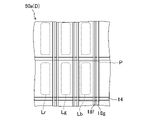
- FIG. 2 is a plan view of the display area of the organic EL display device according to the first embodiment of the invention.
- FIG. 3 is a cross-sectional view of the display area of the organic EL display device according to the first embodiment of the invention.
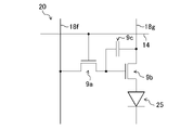
- FIG. 4 is an equivalent circuit diagram of a TFT layer that constitutes the organic EL display device according to the first embodiment of the present invention.
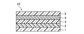
- FIG. 5 is a cross-sectional view showing an organic EL layer that constitutes the organic EL display device according to the first embodiment of the present invention.
- FIG. 6 is a plan view of a first inspection section that constitutes the organic EL display device according to the first embodiment of the present invention.
- FIG. 7 is a cross-sectional view of the first inspection section taken along line VII-VII in FIG.
- FIG. 8 is a plan view of a second inspection section that constitutes the organic EL display device according to the first embodiment of the present invention.
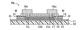
- 9 is a cross-sectional view of the second inspection section taken along line IX-IX in FIG. 8.
- FIG. 10 is a graph showing waveforms of current-voltage characteristics in an example of the organic EL display device according to the first embodiment of the present invention.
- FIG. 11 is a graph showing waveforms of current-voltage characteristics in a comparative example of the organic EL display device according to the first embodiment of the invention.
- FIG. 12 is a plan view showing a schematic configuration of an organic EL display device according to a second embodiment of the invention.
- FIG. 1 is a plan view showing a schematic configuration of the organic EL display device 50a of this embodiment.
- 2 and 3 are a plan view and a cross-sectional view of the display area D of the organic EL display device 50a.
- FIG. 4 is an equivalent circuit diagram of the TFT layer 20 forming the organic EL display device 50a.
- FIG. 5 is a cross-sectional view showing the organic EL layer 23 forming the organic EL display device 50a.
- FIG. 6 is a plan view of the first inspection portion Ra that constitutes the organic EL display device 50a.
- 7 is a cross-sectional view of the first inspection portion Ra taken along line VII--VII in FIG.
- FIG. 8 is a plan view of the second inspection section Rb that constitutes the organic EL display device 50a.
- 9 is a cross-sectional view of the second inspection portion Rb taken along line IX-IX in FIG. 10 and 11 are graphs showing waveforms of current-voltage characteristics in the example and comparative example of the organic EL display device 50a.
- the organic EL display device 50a includes, for example, a rectangular display area D for displaying an image, and a frame area F provided around the display area D in a frame shape.
- the rectangular display area D is exemplified, but the rectangular shape includes, for example, a shape with arc-shaped sides, a shape with arc-shaped corners, and a shape with arc-shaped corners.
- a substantially rectangular shape such as a shape with a notch is also included.
- a plurality of sub-pixels P are arranged in a matrix. Further, in the display region D, as shown in FIG. 2, for example, sub-pixels P having a red light-emitting region Lr for displaying red, sub-pixels P having a green light-emitting region Lg for displaying green, and a sub-pixel P having a blue light-emitting region Lb for displaying blue is provided so as to be adjacent to each other. In addition, in the display area D, for example, one pixel is configured by three adjacent sub-pixels P each having a red light emitting area Lr, a green light emitting area Lg, and a blue light emitting area Lb.
- a terminal portion T in which a plurality of terminals are arranged is provided at the lower end portion of the frame area F in FIG.
- a bending portion B that can be bent at 180° (U-shaped) with the horizontal direction in FIG. It is provided so as to extend in the middle lateral direction).
- inspection portions R are provided at portions corresponding to the four corners of the display area D, respectively.
- the inspection unit R includes a first inspection unit Ra and a second inspection unit Rb provided as TEGs adjacent to each other with an interval of about 0.5 mm, for example. The specific configuration of the first inspection unit Ra and the second inspection unit Rb will be described later.
- the organic EL display device 50a includes a resin substrate layer 10 provided as a base substrate, a TFT layer 20 provided on the resin substrate layer 10, and a light emitting element layer provided on the TFT layer 20. and a sealing film 35 provided on the organic EL element layer 30 .
- the resin substrate layer 10 is made of, for example, polyimide resin.
- the TFT layer 20 includes a base coat film 11 provided on the resin substrate layer 10, a plurality of first TFTs 9a, a plurality of second TFTs 9b and a plurality of capacitors 9c provided on the base coat film 11; A flattening film 19 is provided on each first TFT 9a, each second TFT 9b, and each capacitor 9c.
- a base coat film 11, semiconductor layers 12a and 12b, a gate insulating film 13, a gate line 14 see FIG.
- gate electrodes 14a and 14b and A first wiring layer such as a lower conductive layer 14c, a first interlayer insulating film 15, an upper conductive layer 16, a second interlayer insulating film 17, a source line 18f (see FIG. 2), source electrodes 18a and 18c, drains A second wiring layer such as the electrodes 18b and 18d and the power supply line 18g, and a planarizing film 19 are laminated on the resin substrate layer 10 in this order.
- a plurality of gate lines 14 are provided so as to extend parallel to each other in the horizontal direction in the drawings.
- the TFT layer 20 as shown in FIGS.
- each sub-pixel P is provided with a first TFT 9a, a second TFT 9b and a capacitor 9c.
- the base coat film 11, the gate insulating film 13, the first interlayer insulating film 15, and the second interlayer insulating film 17 are composed of, for example, a single layer film or a laminated film of inorganic insulating films such as silicon nitride, silicon oxide, and silicon oxynitride. ing.
- the first TFT 9a and the second TFT 9b are p-type TFTs in which semiconductor layers 12a and 12b, which will be described later, are doped with an impurity such as boron, for example.
- the first TFT 9a is electrically connected to the corresponding gate line 14 and source line 18f in each sub-pixel P, as shown in FIG.
- the first TFT 9a includes a semiconductor layer 12a, a gate insulating film 13, a gate electrode 14a, a first interlayer insulating film 15, a second interlayer insulating film 17, and a semiconductor layer 12a, a gate insulating film 13, a gate electrode 14a, which are provided on the base coat film 11 in this order. It has a source electrode 18a and a drain electrode 18b.
- the semiconductor layer 12a is provided in an island shape on the base coat film 11 and has, for example, a channel region, a source region and a drain region.
- the gate insulating film 13 is provided so as to cover the semiconductor layer 12a.
- the gate electrode 14a is provided on the gate insulating film 13 so as to overlap with the channel region of the semiconductor layer 12a.
- the first interlayer insulating film 15 and the second interlayer insulating film 17 are provided in order so as to cover the gate electrode 14a.
- the source electrode 18a and the drain electrode 18b are provided on the second interlayer insulating film 17 so as to be separated from each other, as shown in FIG.
- the source electrode 18a and the drain electrode 18b are connected through respective contact holes formed in the laminated film of the gate insulating film 13, the first interlayer insulating film 15 and the second interlayer insulating film 17. It is electrically connected to the source region and the drain region of the semiconductor layer 12a.
- the second TFT 9b is electrically connected to the corresponding first TFT 9a and power supply line 18g in each sub-pixel P, as shown in FIG.
- the second TFT 9b includes a semiconductor layer 12b, a gate insulating film 13, a gate electrode 14b, a first interlayer insulating film 15, a second interlayer insulating film 17, and a semiconductor layer 12b, a gate insulating film 13, a gate electrode 14b, and a semiconductor layer 12b. It has a source electrode 18c and a drain electrode 18d.
- the semiconductor layer 12b is provided in an island shape on the base coat film 11 and has, for example, a channel region, a source region and a drain region.
- the gate insulating film 13 is provided so as to cover the semiconductor layer 12b, as shown in FIG.
- the gate electrode 14b is provided on the gate insulating film 13 so as to overlap with the channel region of the semiconductor layer 12b.
- the first interlayer insulating film 15 and the second interlayer insulating film 17 are provided in order so as to cover the gate electrode 14b.
- the source electrode 18c and the drain electrode 18d are provided on the second interlayer insulating film 17 so as to be separated from each other, as shown in FIG.
- the source electrode 18c and the drain electrode 18d are connected through respective contact holes formed in the laminated film of the gate insulating film 13, the first interlayer insulating film 15 and the second interlayer insulating film 17. It is electrically connected to the source region and the drain region of the semiconductor layer 12b.
- the top gate type first TFT 9a and the second TFT 9b are exemplified, but the first TFT 9a and the second TFT 9b may be bottom gate type TFTs.
- the capacitor 9c is electrically connected to the corresponding first TFT 9a and power supply line 18g in each sub-pixel P, as shown in FIG.
- the capacitor 9c includes a lower conductive layer 14c, a first interlayer insulating film 15 provided so as to cover the lower conductive layer 14c, and a lower conductive layer 15 on the first interlayer insulating film 15.
- An upper conductive layer 16 is provided so as to overlap with 14c.
- the upper conductive layer 16 is electrically connected to the power line 18g through a contact hole formed in the second interlayer insulating film 17, as shown in FIG.
- the planarization film 19 has a flat surface in the display area D, and is made of an organic resin material such as polyimide resin, for example.
- the organic EL element layer 30 includes a plurality of organic EL elements 25 as a plurality of light emitting elements arranged in a matrix corresponding to the plurality of sub-pixels P.
- the organic EL element 25 includes, as shown in FIG. 23, and a second electrode 24 provided in common to a plurality of sub-pixels P on the organic EL layer 23 .
- the first electrode 21 is electrically connected to the drain electrode 18d of the second TFT 9b of each sub-pixel P through a contact hole formed in the planarizing film 19, as shown in FIG. Also, the first electrode 21 has a function of injecting holes into the organic EL layer 23 . Further, the first electrode 21 is more preferably made of a material having a large work function in order to improve the efficiency of hole injection into the organic EL layer 23 .
- materials forming the first electrode 21 include silver (Ag), aluminum (Al), vanadium (V), cobalt (Co), nickel (Ni), tungsten (W), and gold (Au).
- the material forming the first electrode 21 may be an alloy such as astatine (At)/astatine oxide (AtO 2 ).
- the material constituting the first electrode 21 is, for example, conductive oxides such as tin oxide (SnO), zinc oxide (ZnO), indium tin oxide (ITO), and indium zinc oxide (IZO). There may be.
- the first electrode 21 may be formed by laminating a plurality of layers made of the above materials.
- Compound materials having a large work function include, for example, indium tin oxide (ITO) and indium zinc oxide (IZO).
- the peripheral end portion of the first electrode 21 is covered with an edge cover 22 provided in a grid pattern in common with the plurality of sub-pixels P.
- examples of the material forming the edge cover 22 include positive photosensitive resins such as polyimide resins, acrylic resins, polysiloxane resins, and novolak resins.
- the organic EL layer 23 includes a hole injection layer 1, a hole transport layer 2, a light-emitting layer 3, an electron transport layer 4 and an electron injection layer 5 which are provided in this order on the first electrode 21. ing.
- the hole injection layer 1 is also called an anode buffer layer, and has the function of bringing the energy levels of the first electrode 21 and the organic EL layer 23 closer to each other and improving the efficiency of hole injection from the first electrode 21 to the organic EL layer 23 .
- materials constituting the hole injection layer 1 include triazole derivatives, oxadiazole derivatives, imidazole derivatives, polyarylalkane derivatives, pyrazoline derivatives, phenylenediamine derivatives, oxazole derivatives, styrylanthracene derivatives, fluorenone derivatives, hydrazone derivatives, stilbene derivatives and the like.
- the hole transport layer 2 has the function of improving the transport efficiency of holes from the first electrode 21 to the organic EL layer 23 .
- Examples of materials constituting the hole transport layer 2 include porphyrin derivatives, aromatic tertiary amine compounds, styrylamine derivatives, polyvinylcarbazole, poly-p-phenylene vinylene, polysilane, triazole derivatives, and oxadiazole.
- the light-emitting layer 3 In the light-emitting layer 3, holes and electrons are injected from the first electrode 21 and the second electrode 24 when a voltage is applied by the first electrode 21 and the second electrode 24, and the holes and electrons recombine. area.
- the light-emitting layer 3 is made of a material with high light-emitting efficiency. Examples of materials constituting the light-emitting layer 3 include metal oxinoid compounds [8-hydroxyquinoline metal complex], naphthalene derivatives, anthracene derivatives, diphenylethylene derivatives, vinylacetone derivatives, triphenylamine derivatives, butadiene derivatives, and coumarin derivatives.
- the electron transport layer 4 has a function of efficiently transferring electrons to the light emitting layer 3 .
- the materials constituting the electron transport layer 4 include, for example, organic compounds such as oxadiazole derivatives, triazole derivatives, benzoquinone derivatives, naphthoquinone derivatives, anthraquinone derivatives, tetracyanoanthraquinodimethane derivatives, diphenoquinone derivatives, and fluorenone derivatives. , silole derivatives, and metal oxinoid compounds.
- the electron injection layer 5 has a function of bringing the energy levels of the second electrode 24 and the organic EL layer 23 close to each other and improving the efficiency of electron injection from the second electrode 24 to the organic EL layer 23. With this function, The driving voltage of the organic EL element 25 can be lowered.
- the electron injection layer 5 is also called a cathode buffer layer.
- examples of materials constituting the electron injection layer 5 include lithium fluoride (LiF), magnesium fluoride (MgF 2 ), calcium fluoride (CaF 2 ), strontium fluoride (SrF 2 ), and barium fluoride.
- inorganic alkali compounds such as (BaF 2 ), aluminum oxide (Al 2 O 3 ), strontium oxide (SrO), and the like.
- the second electrode 24 is provided so as to cover the organic EL layer 23 of each sub-pixel P and the edge cover 22, as shown in FIG. Also, the second electrode 24 has a function of injecting electrons into the organic EL layer 23 . Moreover, the second electrode 24 is more preferably made of a material with a small work function in order to improve the efficiency of injecting electrons into the organic EL layer 23 .
- materials constituting the second electrode 24 include silver (Ag), aluminum (Al), vanadium (V), cobalt (Co), nickel (Ni), tungsten (W), and gold (Au).
- the second electrode 24 is composed of, for example, magnesium (Mg)/copper (Cu), magnesium (Mg)/silver (Ag), sodium (Na)/potassium (K), astatine (At)/astatin oxide (AtO 2 ), lithium (Li)/aluminum (Al), lithium (Li)/calcium (Ca)/aluminum (Al), lithium fluoride (LiF)/calcium (Ca)/aluminum (Al), etc.
- the second electrode 24 may be formed of conductive oxides such as tin oxide (SnO), zinc oxide (ZnO), indium tin oxide (ITO), and indium zinc oxide (IZO). .
- the second electrode 24 may be formed by laminating a plurality of layers made of the above materials.
- materials with a small work function include magnesium (Mg), lithium (Li), lithium fluoride (LiF), magnesium (Mg)/copper (Cu), magnesium (Mg)/silver (Ag), sodium (Na)/potassium (K), lithium (Li)/aluminum (Al), lithium (Li)/calcium (Ca)/aluminum (Al), lithium fluoride (LiF)/calcium (Ca)/aluminum (Al) etc.
- the sealing film 35 is provided on the organic EL element layer 30 so as to cover each organic EL element 25, as shown in FIG.
- the first inorganic sealing film 31 and the second inorganic sealing film 33 are made of, for example, silicon oxide (SiO 2 ), aluminum oxide (Al 2 O 3 ), or trisilicon tetranitride (Si 3 N 4 ). It is composed of an inorganic material such as silicon nitride (SiNx (x is a positive number)) or silicon carbonitride (SiCN).
- the organic sealing film 32 is made of an organic material such as acrylic resin, polyurea resin, parylene resin, polyimide resin, or polyamide resin.
- the first inspection portion Ra includes a first inspection semiconductor layer 12c provided on the base coat film, a gate insulating film 13 laminated in this order on the first inspection semiconductor layer 12c, and a first inspection semiconductor layer 12c.
- the first inspection semiconductor layer 12c is formed in the same layer with the same material as the semiconductor layers 12a and 12b. Also, as shown in FIG.
- the first inspection semiconductor layer 12c is formed in a swastika shape so as to branch in four directions in a plan view. 6 and 7, the first inspection first terminal 18h, the first inspection second terminal 18i, the first inspection third terminal 18j, and the first inspection fourth terminal 18k are connected to the gate insulating film 13, It is electrically connected to the branched ends of the first test semiconductor layer 12c through contact holes Ch, Ci, Cj, and Ck formed in the laminated film of the first interlayer insulating film 15 and the second interlayer insulating film 17, respectively. ing.
- the first inspection section Ra uses the first inspection first terminal 18h, the first inspection second terminal 18i, the first inspection third terminal 18j, and the first inspection fourth terminal 18k to perform a four-terminal resistance measurement method. For example, it is possible to accurately measure the electric resistance of the first inspection semiconductor layer 12c made of polysilicon doped with an impurity such as boron.
- hydrogen H generated from the laminated film of the gate insulating film 13 the first interlayer insulating film 15 and the second interlayer insulating film 17 is transferred to the first inspection semiconductor layer 12c. dangling bonds existing in the Si film are replaced with hydrogen, and defects in the Si film are reduced, so that the electrical resistance of the first inspection semiconductor layer 12c is relatively lowered.
- the second inspection portion Rb includes a second inspection semiconductor layer 12d provided on the base coat film, a gate insulating film 13 laminated in this order on the second inspection semiconductor layer 12d, and a second inspection semiconductor layer 12d.
- the second inspection semiconductor layer 12d is formed in the same layer with the same material as the semiconductor layers 12a and 12b. Moreover, as shown in FIG.
- the second inspection semiconductor layer 12d is formed in a swastika shape so as to branch in four directions in plan view. 8 and 9, the second inspection first terminal 18v, the second inspection second terminal 18w, the second inspection third terminal 18x, and the second inspection fourth terminal 18y are connected to the gate insulating film 13, Through contact holes Cv, Cw, Cx, and Cy formed in the laminated film of the first interlayer insulating film 15 and the second interlayer insulating film 17, they are electrically connected to branched ends of the second inspection semiconductor layer 12d, respectively. ing. In addition, as shown in FIGS.
- the laminated film of the gate insulating film 13, the first interlayer insulating film 15 and the second interlayer insulating film 17 in the second inspection portion Rb has a second inspection first terminal 18v, a A gate insulating film 13, a first interlayer insulating film 15 and a second interlayer insulating film 17 are stacked over the entire region between the second inspection second terminal 18w, the second inspection third terminal 18x and the second inspection fourth terminal 18y.
- An opening M is provided through the membrane.
- the second inspection section Rb uses the second inspection first terminal 18v, the second inspection second terminal 18w, the second inspection third terminal 18x, and the second inspection fourth terminal 18y to perform a four-terminal resistance measurement method.
- the second inspection semiconductor layer 12d made of polysilicon doped with an impurity such as boron.
- an impurity such as boron.
- hydrogen H generated from the laminated film of the gate insulating film 13 the first interlayer insulating film 15 and the second interlayer insulating film 17 is discharged from the opening M. Therefore, dangling bonds existing in the Si film of the second inspection semiconductor layer 12d are difficult to be replaced with hydrogen, and a decrease in defects in the Si film is suppressed. to be higher.
- the opening M penetrating through the laminated film of the gate insulating film 13, the first interlayer insulating film 15, and the second interlayer insulating film 17 is illustrated in a cross-sectional view.
- the insulating film 13, the first interlayer insulating film 15, and the second interlayer insulating film 17 may be provided so as to open upward without penetrating the laminated film.
- the opening M is at least one of the second test first terminal 18v, the second test second terminal 18w, the second test third terminal 18x, and the second test fourth terminal 18y. It may be provided in a dot shape in a part of the region between the two.
- the organic EL display device 50a described above in each sub-pixel P, by inputting a gate signal to the first TFT 9a through the gate line 14, the first TFT 9a is turned on, and the gate electrode of the second TFT 9b is turned on through the source line 18f. 14b and the capacitor 9c are written with a voltage corresponding to the source signal, and a current from the power supply line 18g defined based on the gate voltage of the second TFT 9b is supplied to the organic EL layer 23, whereby the light emitting layer of the organic EL layer 23 3 emits light to display an image. In the organic EL display device 50a, even when the first TFT 9a is turned off, the gate voltage of the second TFT 9b is held by the capacitor 9c. maintained.
- the organic EL display device 50a has an electric resistance of the first inspection semiconductor layer 12c of the first inspection portion Ra provided in the frame region F and a second The characteristics of the first TFT 9a and the second TFT 9b of each sub-pixel P are managed by measuring the electrical resistance of the test semiconductor layer 12d.
- the method for manufacturing the organic EL display device 50a of this embodiment includes a TFT layer forming process, an organic EL element layer forming process, and a sealing film forming process.
- ⁇ TFT layer formation process First, for example, a glass substrate is coated with a non-photosensitive polyimide resin (thickness of about 6 ⁇ m), and then the coating film is pre-baked and post-baked to form the resin substrate layer 10 .
- a silicon oxide film (thickness of about 500 nm) and a silicon nitride film (thickness of about 100 nm) are sequentially formed on the substrate surface on which the resin substrate layer 10 is formed by, for example, a plasma CVD (chemical vapor deposition) method. By doing so, the base coat film 11 is formed.
- an amorphous silicon film (about 50 nm thick) is formed by plasma CVD on the surface of the substrate on which the base coat film 11 is formed, and the amorphous silicon film is crystallized by laser annealing or the like to form a polysilicon film.
- the semiconductor film is patterned to form the semiconductor layers 12a and 12b, the first inspection semiconductor layer 12c, and the second inspection semiconductor layer 12d (semiconductor layer forming step).
- an inorganic insulating film (about 100 nm) such as a silicon oxide film is formed on the substrate surface on which the semiconductor layer 12a and the like are formed by, for example, a plasma CVD method, and a gate insulating film is formed so as to cover the semiconductor layer 12a and the like. 13 is formed (gate insulating film formation step).
- a molybdenum film (about 250 nm thick) is formed by, for example, sputtering on the surface of the substrate on which the gate insulating film 13 is formed. , 14b and the like are formed.
- impurity ions such as boron are doped to partially conduct the semiconductor layers 12a and 12b, and the first inspection semiconductor layer 12c and the second inspection semiconductor layer are formed.
- 12d is made conductive (doping step).
- the first interlayer insulating film 15 is formed by forming a silicon nitride film (thickness of about 100 nm) by plasma CVD, for example, on the surface of the substrate where at least a part of the semiconductor layer 12a and the like is made conductive. (interlayer insulating film formation step).
- the substrate on which the first interlayer insulating film 15 is formed is heat-treated at about 400° C. (first annealing step).
- a molybdenum film (about 250 nm thick) is formed on the heat-treated substrate surface by, for example, sputtering, and the molybdenum film is patterned to form the upper conductive layer 16 .
- a silicon oxide film (thickness of about 300 nm) and a silicon nitride film (thickness of about 200 nm) are sequentially formed on the surface of the substrate on which the upper conductive layer 16 is formed by, for example, plasma CVD, thereby forming a second An interlayer insulating film 17 is formed.
- the gate insulating film 13, the first interlayer insulating film 15 and the second interlayer insulating film 17 are patterned to form the contact holes Ch, Ci, Cj, Ck, Cv, Cw, Cx and Cy and the opening M. formed (laminated film patterning step).
- the substrate in which the contact holes and openings M are formed is heat-treated at about 400° C. (second annealing step). Note that the temperature of the heat treatment performed in the second annealing process may be lower than the temperature of the heat treatment performed in the first annealing process.
- a titanium film (about 50 nm thick), an aluminum film (about 600 nm thick), and a titanium film (about 50 nm thick) are formed in this order on the surface of the substrate subjected to the heat treatment by, for example, a sputtering method. are patterned to form source electrodes 18a and 18c, drain electrodes 18b and 18d, source line 18f, power supply line 18g, first inspection first terminal 18h, first inspection second terminal 18i, and first inspection third terminal 18h. A third wiring layer of the terminal 18j, the first inspection fourth terminal 18k, the second inspection first terminal 18v, the second inspection second terminal 18w, the second inspection third terminal 18x, and the second inspection fourth terminal 18y is formed. .
- the first TFT 9a, the second TFT 9b, the first inspection portion Ra, and the second inspection portion Rb are formed.
- 18i a first inspection third terminal 18j and a first inspection fourth terminal 18k, and a second inspection first terminal 18v, a second inspection second terminal 18w, a second inspection third terminal 18x and a second inspection section Rb.
- a probe pin of an electric resistance measuring device is brought into contact with the second inspection fourth terminal 18y to measure the electric power of the first inspection semiconductor layer 12c of the first inspection portion Ra and the second inspection semiconductor layer 12d of the second inspection portion Rb.
- the characteristics of the first TFT 9a and the second TFT 9b can be managed by measuring the respective resistances and detecting the difference between the electrical resistances.
- the electrical resistance value of the first inspection semiconductor layer 12c of the first inspection portion Ra and the electrical resistance value of the second inspection semiconductor layer 12d of the second inspection portion Rb cannot detect the difference from the electric resistance value of the inspection semiconductor layer (12d).
- the surface of the substrate on which the third wiring layer is formed is coated with a photosensitive polyimide resin (thickness of about 2.5 ⁇ m) by, for example, a spin coating method or a slit coating method.
- a flattening film 19 is formed by performing pre-baking, exposure, development and post-baking.
- the TFT layer 20 can be formed as described above.
- the current of the first TFT 9a and the second TFT 9b formed in the TFT layer 20 is -
- the voltage characteristic waveform has a gentle slope and a relatively large S value, as shown in FIG.
- the first TFT (9a) and the second TFT (9b) As shown in FIG. 11, the waveform of the current-voltage characteristic has a steep slope and a relatively small S value.
- Organic EL element layer forming process A first electrode 21, an edge cover 22, an organic EL layer 23 (hole injection layer 1, hole transport An organic EL element 25 is formed by forming a layer 2, a light-emitting layer 3, an electron transport layer 4, an electron injection layer 5), and a second electrode 24, and an organic EL element layer 30 is formed.
- ⁇ Sealing film forming process> For example, a silicon nitride film, a silicon oxide film, a silicon oxynitride film, or the like is applied on the organic EL element layer 30 formed in the organic EL element layer forming step using a mask so as to cover each organic EL element 25 .
- An inorganic insulating film is deposited by plasma CVD to form the first inorganic sealing film 31 .
- an organic resin material such as an acrylic resin is deposited on the first inorganic sealing film 31 by, for example, an inkjet method to form an organic sealing film 32 .
- an inorganic insulating film such as a silicon nitride film, a silicon oxide film, or a silicon oxynitride film is formed by plasma CVD so as to cover the organic sealing film 32, thereby forming a second inorganic sealing film.
- a sealing film 35 is formed by forming the stop film 33 .
- a laser beam is irradiated from the glass substrate side of the resin substrate layer 10, thereby removing the glass from the lower surface of the resin substrate layer 10.
- the substrate is peeled off, and a protective sheet (not shown) is attached to the lower surface of the resin substrate layer 10 from which the glass substrate has been peeled off.
- the organic EL display device 50a of the present embodiment can be manufactured.
- the first inspection portion Ra and the second inspection portion R provided in the frame region F are provided so as to be adjacent to each other. It has an inspection part Rb.
- the first inspection portion Ra hydrogen H generated from the laminated film of the gate insulating film 13, the first interlayer insulating film 15 and the second interlayer insulating film 17 penetrates into the Si film of the first inspection semiconductor layer 12c. , dangling bonds existing in the Si film are replaced with hydrogen, and defects in the Si film are reduced, so that the electric resistance of the first inspection semiconductor layer 12c is relatively lowered.
- the laminated film of the gate insulating film 13, the first interlayer insulating film 15, and the second interlayer insulating film 17 is provided with the second inspection first terminal 18v, the second inspection second terminal 18w, and the second inspection terminal 18w.
- An upward opening M is provided between at least one of the third inspection terminal 18x and the fourth inspection terminal 18y.
- the hydrogen H generated from the laminated film of the gate insulating film 13, the first interlayer insulating film 15, and the second interlayer insulating film 17 is discharged from the opening M, so that the second inspection semiconductor layer
- the dangling bonds existing in the Si film 12d are not easily replaced with hydrogen, and the reduction of defects in the Si film is suppressed, so that the electric resistance of the second inspection semiconductor layer 12d is relatively high.
- the difference between the electrical resistance of the first inspection semiconductor layer 12c of the first inspection portion Ra and the electrical resistance of the second inspection semiconductor layer 12d of the second inspection portion Rb can be reliably detected.
- the first organic EL display device 50a is It is possible to presume the manufacturing process carried out during manufacturing, that is, the manufacturing process in which the gate insulating film forming process, the interlayer insulating film forming process, the first annealing process, the laminated film patterning process, and the second annealing process are sequentially performed.
- the stacked film of the gate insulating film 13, the first interlayer insulating film 15, and the second interlayer insulating film 17 has the second The gate insulation film 13, the first interlayer insulation film 15 and the second insulation film 15 are formed on the entire regions between the second inspection first terminal 18v, the second inspection second terminal 18w, the second inspection third terminal 18x and the second inspection fourth terminal 18y.
- An opening M is provided so as to penetrate the laminated film of the two-layer insulating film 17.
- the hydrogen H generated from the laminated film of the gate insulating film 13, the first interlayer insulating film 15 and the second interlayer insulating film 17 is further discharged from the opening M, dangling bonds existing in the Si film of the second inspection semiconductor layer 12d are more difficult to be replaced with hydrogen, and the reduction of defects in the Si film is suppressed.
- the electric resistance of the second inspection semiconductor layer 12d becomes relatively higher. This makes it possible to more reliably detect the difference between the electrical resistance of the first inspection semiconductor layer 12c of the first inspection portion Ra and the electrical resistance of the second inspection semiconductor layer 12d of the second inspection portion Rb.
- the gate insulating film forming process, the interlayer insulating film forming process, the first annealing process, the laminated film patterning process and the second annealing are performed. Since the processes are performed in order, in the first annealing process, defects generated in the doping process in the Si films of the semiconductor layers 12a and 12b can be repaired, and dangling bonds existing in the Si films can be replaced with hydrogen. It can be performed. Then, in the second annealing step, hydrogen can be desorbed from the Si films of the semiconductor layers 12a and 12b.
- the hydrogen desorption in the second annealing step is performed uniformly within the substrate plane, variations in the S value can be reduced.
- the organic EL display device 50a of the present embodiment and the manufacturing method thereof if the temperature of the heat treatment performed in the second annealing step is lower than the temperature of the heat treatment performed in the first annealing step, an excessive increase in the S value is suppressed. can do.
- FIG. 12 shows a second embodiment of the display device and its manufacturing method according to the present invention.
- FIG. 12 is a plan view showing a schematic configuration of the organic EL display device 50b of this embodiment.
- the same parts as in FIGS. 1 to 11 are denoted by the same reference numerals, and detailed description thereof will be omitted.
- the organic EL display device 50a in which the inspection section R is provided in the portion corresponding to the corner of the display area D in the frame area F is exemplified.
- An organic EL display device 50b in which an inspection section R is provided in the vicinity of a circuit E is illustrated.
- the organic EL display device 50b includes a display region D and a frame region F provided around the display region D, like the organic EL display device 50a of the first embodiment.
- the display area D is provided in a substantially rectangular shape with arcuate corners.
- a peripheral circuit E such as a gate driver (gate drive circuit) and an emission driver is monolithically provided in the frame area F.
- the peripheral circuit E is provided, for example, along two sides facing each other around the display area D formed in a substantially rectangular shape with arc-shaped corners, and arc-shaped ends of the two sides. As shown in FIG. 12, it is provided so as to bend stepwise in a plan view along the arc-shaped portion. 12, the inspection portion R including the first inspection portion Ra and the second inspection portion Rb is provided in the valley portion outside the bent portion of the peripheral circuit E. As shown in FIG.
- the organic EL display device 50b includes, in the display area D, the resin substrate layer 10, the TFT layer 20 provided on the resin substrate layer 10, and the TFT layer 20; 20 and a sealing film 35 provided on the organic EL element layer 30 .
- the organic EL display device 50b described above has flexibility, and in each sub-pixel P, the organic EL layer 23 is formed via the first TFT 9a and the second TFT 9b.
- the light-emitting layer 3 is caused to emit light appropriately to display an image.
- the electrical resistance of the first inspection semiconductor layer 12c of the first inspection portion Ra provided in the frame region F, and the The characteristics of the first TFT 9a and the second TFT 9b of each sub-pixel P are managed by measuring the electric resistance of the second inspection semiconductor layer 12d of the two inspection portions Rb.
- the organic EL display device 50b of the present embodiment can be manufactured by changing the position where the inspection section R is formed in the manufacturing method of the organic EL display device 50a of the first embodiment.
- the first inspection portion Ra and the second inspection portion R provided in the frame region F are provided so as to be adjacent to each other. It has an inspection part Rb.
- the first inspection portion Ra hydrogen H generated from the laminated film of the gate insulating film 13, the first interlayer insulating film 15 and the second interlayer insulating film 17 penetrates into the Si film of the first inspection semiconductor layer 12c. , dangling bonds existing in the Si film are replaced with hydrogen, and defects in the Si film are reduced, so that the electric resistance of the first inspection semiconductor layer 12c is relatively lowered.
- the laminated film of the gate insulating film 13, the first interlayer insulating film 15, and the second interlayer insulating film 17 is provided with the second inspection first terminal 18v, the second inspection second terminal 18w, and the second inspection terminal 18w.
- An upward opening M is provided between at least one of the third inspection terminal 18x and the fourth inspection terminal 18y.
- the hydrogen H generated from the laminated film of the gate insulating film 13, the first interlayer insulating film 15, and the second interlayer insulating film 17 is discharged from the opening M, so that the second inspection semiconductor layer
- the dangling bonds existing in the Si film 12d are not easily replaced with hydrogen, and the reduction of defects in the Si film is suppressed, so that the electric resistance of the second inspection semiconductor layer 12d is relatively high.
- the difference between the electrical resistance of the first inspection semiconductor layer 12c of the first inspection portion Ra and the electrical resistance of the second inspection semiconductor layer 12d of the second inspection portion Rb can be reliably detected.
- the first organic EL display device 50b can be It is possible to presume the manufacturing process carried out during manufacturing, that is, the manufacturing process in which the gate insulating film forming process, the interlayer insulating film forming process, the first annealing process, the laminated film patterning process, and the second annealing process are sequentially performed.
- the inspection section R is provided in the vicinity of the peripheral circuit E in which the TFTs are formed in the frame region F, the density of the wiring pattern becomes close to the density of the wiring pattern of each sub-pixel P, and the characteristics of the first TFT 9a and the second TFT 9b of the TFT layer 20 can be managed more reliably by process inspection.
- an organic EL layer having a five-layer laminate structure of a hole injection layer, a hole transport layer, a light-emitting layer, an electron transport layer, and an electron injection layer was exemplified. It may have a three-layered structure of a layer-cum-hole-transporting layer, a light-emitting layer, and an electron-transporting layer-cum-electron-injecting layer.
- the organic EL display device in which the first electrode is the anode and the second electrode is the cathode was exemplified. , and can also be applied to an organic EL display device in which the second electrode is an anode.
- the organic EL display device in which the electrode of the TFT connected to the first electrode is used as the drain electrode is exemplified. It can also be applied to a so-called organic EL display device.
- an organic EL display device was described as an example of a display device.
- QLED Quantum-dot light emitting diode
- the present invention is useful for flexible display devices.
- Second inspection portion 9a First TFT (first 1 thin film transistor) 9b second TFT (first thin film transistor) 10 resin substrate layer (base substrate) 12a, 12b semiconductor layer 12c first inspection semiconductor layer 12d second inspection semiconductor layer 13 gate insulating film 14 gate line (first wiring layer) 14a, 14b gate electrodes (first wiring layer) 14c lower conductive layer (first wiring layer) 15 First interlayer insulating film 17 Second interlayer insulating films 18a, 18c Source electrode (second wiring layer) 18b, 18d drain electrode (second wiring layer) 18f source line (second wiring layer) 18g power line (second wiring layer) 18h First inspection first terminal 18i First inspection second terminal 18j First inspection third terminal 18k First inspection fourth terminal 18v Second inspection first terminal 18w Second inspection second terminal 18x Second inspection third terminal 18y Second inspection fourth terminal 20 TFT layer (thin film transistor
Landscapes
- Engineering & Computer Science (AREA)
- Manufacturing & Machinery (AREA)
- Microelectronics & Electronic Packaging (AREA)
- Physics & Mathematics (AREA)
- General Physics & Mathematics (AREA)
- Theoretical Computer Science (AREA)
- Electroluminescent Light Sources (AREA)
- Devices For Indicating Variable Information By Combining Individual Elements (AREA)
Abstract
Description
図1~図11は、本発明に係る表示装置及びその製造方法の第1の実施形態を示している。なお、以下の各実施形態では、発光素子を備えた表示装置として、有機EL素子を備えた有機EL表示装置を例示する。ここで、図1は、本実施形態の有機EL表示装置50aの概略構成を示す平面図である。また、図2及び図3は、有機EL表示装置50aの表示領域Dの平面図及び断面図である。また、図4は、有機EL表示装置50aを構成するTFT層20の等価回路図である。また、図5は、有機EL表示装置50aを構成する有機EL層23を示す断面図である。また、図6は、有機EL表示装置50aを構成する第1検査部Raの平面図である。また、図7は、図6中のVII-VII線に沿った第1検査部Raの断面図である。また、図8は、有機EL表示装置50aを構成する第2検査部Rbの平面図である。また、図9は、図8中のIX-IX線に沿った第2検査部Rbの断面図である。また、図10及び図11は、有機EL表示装置50aの実施例及び比較例における電流-電圧特性の波形を示すグラフである。
まず、例えば、ガラス基板上に非感光性のポリイミド樹脂(厚さ6μm程度)を塗布した後、その塗布膜に対して、プリベーク及びポストベークを行うことにより、樹脂基板層10を形成する。
上記TFT層形成工程で形成されたTFT層20の平坦化膜19上に、周知の方法を用いて、第1電極21、エッジカバー22、有機EL層23(正孔注入層1、正孔輸送層2、発光層3、電子輸送層4、電子注入層5)及び第2電極24を形成することにより、有機EL素子25を形成して、有機EL素子層30を形成する。
上記有機EL素子層形成工程で形成された有機EL素子層30上に、各有機EL素子25を覆うように、マスクを用いて、例えば、窒化シリコン膜、酸化シリコン膜、酸窒化シリコン膜等の無機絶縁膜をプラズマCVD法により成膜して、第1無機封止膜31を形成する。
図12は、本発明に係る表示装置及びその製造方法の第2の実施形態を示している。ここで、図12は、本実施形態の有機EL表示装置50bの概略構成を示す平面図である。なお、以下の各実施形態において、図1~図11と同じ部分については同じ符号を付して、その詳細な説明を省略する。
上記各実施形態では、正孔注入層、正孔輸送層、発光層、電子輸送層及び電子注入層の5層積層構造の有機EL層を例示したが、有機EL層は、例えば、正孔注入層兼正孔輸送層、発光層、及び電子輸送層兼電子注入層の3層積層構造であってもよい。
D 表示領域
E 周辺回路
F 額縁領域
M 開口部
P サブ画素
R 検査部
Ra 第1検査部
Rb 第2検査部
9a 第1TFT(第1薄膜トランジスタ)
9b 第2TFT(第1薄膜トランジスタ)
10 樹脂基板層(ベース基板)
12a,12b 半導体層
12c 第1検査半導体層
12d 第2検査半導体層
13 ゲート絶縁膜
14 ゲート線(第1配線層)
14a,14b ゲート電極(第1配線層)
14c 下部導電層(第1配線層)
15 第1層間絶縁膜
17 第2層間絶縁膜
18a,18c ソース電極(第2配線層)
18b,18d ドレイン電極(第2配線層)
18f ソース線(第2配線層)
18g 電源線(第2配線層)
18h 第1検査第1端子
18i 第1検査第2端子
18j 第1検査第3端子
18k 第1検査第4端子
18v 第2検査第1端子
18w 第2検査第2端子
18x 第2検査第3端子
18y 第2検査第4端子
20 TFT層(薄膜トランジスタ層)
25 有機EL素子(有機エレクトロルミネッセンス素子、発光素子)
30 有機EL素子層(発光素子層)
50a,50b 有機EL表示装置
Claims (13)
- ベース基板と、
上記ベース基板上に設けられ、半導体層、ゲート絶縁膜、第1配線層、層間絶縁膜及び第2配線層が順に積層された薄膜トランジスタ層と、
上記薄膜トランジスタ層上に設けられ、表示領域を構成する複数のサブ画素に対応して複数の発光素子が配列された発光素子層とを備え、
上記表示領域の周囲には、額縁領域が設けられ、
上記額縁領域には、検査部が設けられた表示装置であって、
上記検査部は、互いに隣り合うように設けられた第1検査部及び第2検査部を備え、
上記第1検査部は、上記半導体層と同一材料により同一層に形成された第1検査半導体層と、該第1検査半導体層を覆うように設けられた上記ゲート絶縁膜及び上記層間絶縁膜と、該層間絶縁膜上に設けられ、上記ゲート絶縁膜及び上記層間絶縁膜の積層膜に形成された各コンタクトホールを介して上記第1検査半導体層に電気的に接続された第1検査第1端子、第1検査第2端子、第1検査第3端子及び第1検査第4端子とを備え、
上記第2検査部は、上記半導体層と同一材料により同一層に形成された第2検査半導体層と、該第2検査半導体層を覆うように設けられた上記ゲート絶縁膜及び上記層間絶縁膜と、該層間絶縁膜上に設けられ、上記ゲート絶縁膜及び上記層間絶縁膜の積層膜に形成された各コンタクトホールを介して上記第2検査半導体層に電気的に接続された第2検査第1端子、第2検査第2端子、第2検査第3端子及び第2検査第4端子とを備え、
上記第2検査部における上記ゲート絶縁膜及び上記層間絶縁膜の積層膜には、上記第2検査第1端子、上記第2検査第2端子、上記第2検査第3端子及び上記第2検査第4端子の少なくとも1つの間で上方に開口した開口部が設けられていることを特徴とする表示装置。 - 請求項1に記載された表示装置において、
上記開口部は、上記第2検査部における上記ゲート絶縁膜及び上記層間絶縁膜の積層膜を貫通するように設けられていることを特徴とする表示装置。 - 請求項1又は2に記載された表示装置において、
上記開口部は、上記第2検査第1端子、上記第2検査第2端子、上記第2検査第3端子及び上記第2検査第4端子の各間の領域全体に設けられていることを特徴とする表示装置。 - 請求項1~3の何れか1つに記載された表示装置において、
上記第1検査半導体層及び上記第2検査半導体層は、平面視で4方向に分岐するようにそれぞれ形成され、
上記第1検査第1端子、上記第1検査第2端子、上記第1検査第3端子及び上記第1検査第4端子は、上記第1検査半導体層の分岐した先に電気的にそれぞれ接続され、
上記第2検査第1端子、上記第2検査第2端子、上記第2検査第3端子及び上記第2検査第4端子は、上記第2検査半導体層の分岐した先に電気的にそれぞれ接続されていることを特徴とする表示装置。 - 請求項1~4の何れか1つに記載された表示装置において、
上記薄膜トランジスタ層に設けられた薄膜トランジスタは、p型の薄膜トランジスタであることを特徴とする表示装置。 - 請求項1~5の何れか1つに記載された表示装置において、
上記検査部は、上記額縁領域に複数設けられていることを特徴とする表示装置。 - 請求項6に記載された表示装置において、
上記表示領域は、矩形状に設けられ、
上記検査部は、上記額縁領域における上記表示領域の4つの角部に対応する部分にそれぞれ設けられていることを特徴とする表示装置。 - 請求項1~5の何れか1つに記載された表示装置において、
上記表示領域は、角部が円弧状の略矩状に設けられ、
上記額縁領域には、上記表示領域の周囲に沿って周辺回路が設けられ、
上記周辺回路は、上記表示領域の周囲の円弧状の部分において、該円弧状の部分に沿って平面視で階段状に屈曲するように設けられ、
上記検査部は、上記周辺回路の屈曲した部分の外側の谷部に設けられていることを特徴とする表示装置。 - 請求項8に記載された表示装置において、
上記周辺回路は、ゲート駆動回路であることを特徴とする表示装置。 - 請求項1~9の何れか1つに記載された表示装置において、
上記各発光素子は、有機エレクトロルミネッセンス素子であることを特徴とする表示装置。 - 請求項1~10の何れか1つに記載された表示装置を製造する方法であって、
上記半導体層を形成する際に上記第1検査半導体層及び上記第2検査半導体層を形成する半導体層形成工程と、
上記半導体層形成工程で形成された上記半導体層、上記第1検査半導体層及び上記第2検査半導体層を覆うように上記ゲート絶縁膜を形成するゲート絶縁膜形成工程と、
上記ゲート絶縁膜形成工程で形成された上記ゲート絶縁膜上に層間絶縁膜を形成する層間絶縁膜形成工程と、
上記層間絶縁膜形成工程の後に熱処理を行う第1アニール工程と、
上記第1アニール工程の後に、上記ゲート絶縁膜及び上記層間絶縁膜の積層膜をパターニングして、上記コンタクトホール及び上記開口部を形成する積層膜パターニング工程と、
上記積層膜パターニング工程の後に熱処理を行う第2アニール工程とを備えることを特徴とする表示装置の製造方法。 - 請求項11に記載された表示装置の製造方法において、
上記ゲート絶縁膜形成工程及び上記層間絶縁膜形成工程の間に上記ゲート絶縁膜を介して上記半導体層、上記第1検査半導体層及び上記第2検査半導体層に不純物をドーピングするドーピング工程を備えることを特徴とする表示装置の製造方法。 - 請求項11又は12に記載された表示装置の製造方法において、
上記第2アニール工程で行う熱処理の温度を上記第1アニール工程で行う熱処理の温度よりも低くすることを特徴とする表示装置の製造方法。
Priority Applications (3)
| Application Number | Priority Date | Filing Date | Title |
|---|---|---|---|
| PCT/JP2021/012669 WO2022201461A1 (ja) | 2021-03-25 | 2021-03-25 | 表示装置及びその製造方法 |
| US18/281,393 US20240155901A1 (en) | 2021-03-25 | 2021-03-25 | Display device and production method for same |
| CN202180095868.2A CN117256051A (zh) | 2021-03-25 | 2021-03-25 | 显示装置及其制造方法 |
Applications Claiming Priority (1)
| Application Number | Priority Date | Filing Date | Title |
|---|---|---|---|
| PCT/JP2021/012669 WO2022201461A1 (ja) | 2021-03-25 | 2021-03-25 | 表示装置及びその製造方法 |
Publications (1)
| Publication Number | Publication Date |
|---|---|
| WO2022201461A1 true WO2022201461A1 (ja) | 2022-09-29 |
Family
ID=83396593
Family Applications (1)
| Application Number | Title | Priority Date | Filing Date |
|---|---|---|---|
| PCT/JP2021/012669 Ceased WO2022201461A1 (ja) | 2021-03-25 | 2021-03-25 | 表示装置及びその製造方法 |
Country Status (3)
| Country | Link |
|---|---|
| US (1) | US20240155901A1 (ja) |
| CN (1) | CN117256051A (ja) |
| WO (1) | WO2022201461A1 (ja) |
Cited By (1)
| Publication number | Priority date | Publication date | Assignee | Title |
|---|---|---|---|---|
| EP4567426A1 (en) | 2023-12-05 | 2025-06-11 | Helmholtz Zentrum München - Deutsches Forschungszentrum für Gesundheit und Umwelt (GmbH) | A nanoparticle, a suspension comprising nanoparticles, and related method |
Families Citing this family (1)
| Publication number | Priority date | Publication date | Assignee | Title |
|---|---|---|---|---|
| KR102569929B1 (ko) * | 2018-07-02 | 2023-08-24 | 삼성디스플레이 주식회사 | 디스플레이 장치 |
Citations (5)
| Publication number | Priority date | Publication date | Assignee | Title |
|---|---|---|---|---|
| WO2012118039A1 (ja) * | 2011-02-28 | 2012-09-07 | 株式会社神戸製鋼所 | 表示装置もしくは半導体装置用Al合金膜、Al合金膜を備えた表示装置もしくは半導体装置、およびスパッタリングターゲット |
| JP2015073094A (ja) * | 2013-09-05 | 2015-04-16 | 株式会社半導体エネルギー研究所 | コンタクト抵抗測定パターンおよび半導体装置 |
| JP2015212420A (ja) * | 2015-06-08 | 2015-11-26 | 株式会社神戸製鋼所 | 表示装置もしくは半導体装置用Al合金膜 |
| JP2019135694A (ja) * | 2018-02-05 | 2019-08-15 | 株式会社神戸製鋼所 | 有機elディスプレイ用の反射アノード電極 |
| JP2020194758A (ja) * | 2019-05-30 | 2020-12-03 | 株式会社神戸製鋼所 | 有機elディスプレイ用の反射アノード電極 |
Family Cites Families (9)
| Publication number | Priority date | Publication date | Assignee | Title |
|---|---|---|---|---|
| KR100815765B1 (ko) * | 2007-05-15 | 2008-03-20 | 삼성에스디아이 주식회사 | 발광표시장치 및 그의 제조방법 |
| KR102253966B1 (ko) * | 2013-12-09 | 2021-05-18 | 엘지디스플레이 주식회사 | 유기전계 발광표시장치, 이의 제조방법 및 검사방법 |
| KR102456436B1 (ko) * | 2015-02-17 | 2022-10-20 | 삼성디스플레이 주식회사 | 유기 발광 표시 장치 |
| CN105576037B (zh) * | 2016-01-08 | 2018-11-13 | 京东方科技集团股份有限公司 | 薄膜晶体管及其制作和测试方法、阵列基板和显示装置 |
| KR102497283B1 (ko) * | 2017-08-17 | 2023-02-08 | 삼성디스플레이 주식회사 | 디스플레이 장치 |
| US11088138B2 (en) * | 2017-11-29 | 2021-08-10 | The Industry & Academic Cooperation In Chungnam National University (Iac) | Semiconductor device for testing characteristics of transistors and method for testing semiconductor device |
| KR102912632B1 (ko) * | 2019-08-30 | 2026-01-14 | 삼성디스플레이 주식회사 | 디스플레이 장치 |
| KR20210104196A (ko) * | 2020-02-14 | 2021-08-25 | 삼성디스플레이 주식회사 | 표시 장치 |
| KR102899241B1 (ko) * | 2020-07-31 | 2025-12-11 | 삼성디스플레이 주식회사 | 디스플레이 장치 |
-
2021
- 2021-03-25 US US18/281,393 patent/US20240155901A1/en active Pending
- 2021-03-25 CN CN202180095868.2A patent/CN117256051A/zh active Pending
- 2021-03-25 WO PCT/JP2021/012669 patent/WO2022201461A1/ja not_active Ceased
Patent Citations (5)
| Publication number | Priority date | Publication date | Assignee | Title |
|---|---|---|---|---|
| WO2012118039A1 (ja) * | 2011-02-28 | 2012-09-07 | 株式会社神戸製鋼所 | 表示装置もしくは半導体装置用Al合金膜、Al合金膜を備えた表示装置もしくは半導体装置、およびスパッタリングターゲット |
| JP2015073094A (ja) * | 2013-09-05 | 2015-04-16 | 株式会社半導体エネルギー研究所 | コンタクト抵抗測定パターンおよび半導体装置 |
| JP2015212420A (ja) * | 2015-06-08 | 2015-11-26 | 株式会社神戸製鋼所 | 表示装置もしくは半導体装置用Al合金膜 |
| JP2019135694A (ja) * | 2018-02-05 | 2019-08-15 | 株式会社神戸製鋼所 | 有機elディスプレイ用の反射アノード電極 |
| JP2020194758A (ja) * | 2019-05-30 | 2020-12-03 | 株式会社神戸製鋼所 | 有機elディスプレイ用の反射アノード電極 |
Cited By (1)
| Publication number | Priority date | Publication date | Assignee | Title |
|---|---|---|---|---|
| EP4567426A1 (en) | 2023-12-05 | 2025-06-11 | Helmholtz Zentrum München - Deutsches Forschungszentrum für Gesundheit und Umwelt (GmbH) | A nanoparticle, a suspension comprising nanoparticles, and related method |
Also Published As
| Publication number | Publication date |
|---|---|
| CN117256051A (zh) | 2023-12-19 |
| US20240155901A1 (en) | 2024-05-09 |
Similar Documents
| Publication | Publication Date | Title |
|---|---|---|
| US11957015B2 (en) | Display device | |
| WO2019130480A1 (ja) | 表示装置及びその製造方法 | |
| WO2019163030A1 (ja) | 表示装置及びその製造方法 | |
| WO2021079412A1 (ja) | 表示装置 | |
| US11871615B2 (en) | Display device and method for manufacturing same | |
| US11985876B2 (en) | Display device | |
| US11508792B2 (en) | Display device and method for manufacturing display device | |
| WO2022201487A1 (ja) | 表示装置 | |
| WO2019186702A1 (ja) | 表示装置 | |
| WO2022201461A1 (ja) | 表示装置及びその製造方法 | |
| US12089444B2 (en) | Display device and method for manufacturing same | |
| US20240397769A1 (en) | Display device | |
| WO2020008588A1 (ja) | 表示装置及びその製造方法 | |
| WO2020039555A1 (ja) | 表示装置 | |
| WO2019186812A1 (ja) | 表示装置及びその製造方法 | |
| WO2020179026A1 (ja) | 表示装置及びその製造方法 | |
| WO2023073781A1 (ja) | 表示装置 | |
| WO2023007549A1 (ja) | 表示装置の製造方法 | |
| CN115836588B (zh) | 显示装置 | |
| US20240357887A1 (en) | Display device | |
| US12310194B2 (en) | Display device with interlayer insulating film having column slit for power-source line | |
| WO2019142261A1 (ja) | 表示装置及びその製造方法 | |
| US12029083B2 (en) | Display device | |
| US20230329038A1 (en) | Display device and method for manufacturing same | |
| WO2026022895A1 (ja) | 表示装置 |
Legal Events
| Date | Code | Title | Description |
|---|---|---|---|
| 121 | Ep: the epo has been informed by wipo that ep was designated in this application |
Ref document number: 21933066 Country of ref document: EP Kind code of ref document: A1 |
|
| WWE | Wipo information: entry into national phase |
Ref document number: 18281393 Country of ref document: US |
|
| WWE | Wipo information: entry into national phase |
Ref document number: 202180095868.2 Country of ref document: CN |
|
| NENP | Non-entry into the national phase |
Ref country code: DE |
|
| 122 | Ep: pct application non-entry in european phase |
Ref document number: 21933066 Country of ref document: EP Kind code of ref document: A1 |
|
| NENP | Non-entry into the national phase |
Ref country code: JP |