WO2022201448A1 - スイッチング電源装置および電力供給システム - Google Patents
スイッチング電源装置および電力供給システム Download PDFInfo
- Publication number
- WO2022201448A1 WO2022201448A1 PCT/JP2021/012621 JP2021012621W WO2022201448A1 WO 2022201448 A1 WO2022201448 A1 WO 2022201448A1 JP 2021012621 W JP2021012621 W JP 2021012621W WO 2022201448 A1 WO2022201448 A1 WO 2022201448A1
- Authority
- WO
- WIPO (PCT)
- Prior art keywords
- load current
- power supply
- switching
- voltage
- current
- Prior art date
- Legal status (The legal status is an assumption and is not a legal conclusion. Google has not performed a legal analysis and makes no representation as to the accuracy of the status listed.)
- Ceased
Links
Images







Classifications
-
- H—ELECTRICITY
- H02—GENERATION; CONVERSION OR DISTRIBUTION OF ELECTRIC POWER
- H02M—APPARATUS FOR CONVERSION BETWEEN AC AND AC, BETWEEN AC AND DC, OR BETWEEN DC AND DC, AND FOR USE WITH MAINS OR SIMILAR POWER SUPPLY SYSTEMS; CONVERSION OF DC OR AC INPUT POWER INTO SURGE OUTPUT POWER; CONTROL OR REGULATION THEREOF
- H02M3/00—Conversion of DC power input into DC power output
- H02M3/01—Resonant DC/DC converters
-
- H—ELECTRICITY
- H02—GENERATION; CONVERSION OR DISTRIBUTION OF ELECTRIC POWER
- H02M—APPARATUS FOR CONVERSION BETWEEN AC AND AC, BETWEEN AC AND DC, OR BETWEEN DC AND DC, AND FOR USE WITH MAINS OR SIMILAR POWER SUPPLY SYSTEMS; CONVERSION OF DC OR AC INPUT POWER INTO SURGE OUTPUT POWER; CONTROL OR REGULATION THEREOF
- H02M1/00—Details of apparatus for conversion
- H02M1/0003—Details of control, feedback or regulation circuits
- H02M1/0009—Devices or circuits for detecting current in a converter
-
- H—ELECTRICITY
- H02—GENERATION; CONVERSION OR DISTRIBUTION OF ELECTRIC POWER
- H02M—APPARATUS FOR CONVERSION BETWEEN AC AND AC, BETWEEN AC AND DC, OR BETWEEN DC AND DC, AND FOR USE WITH MAINS OR SIMILAR POWER SUPPLY SYSTEMS; CONVERSION OF DC OR AC INPUT POWER INTO SURGE OUTPUT POWER; CONTROL OR REGULATION THEREOF
- H02M3/00—Conversion of DC power input into DC power output
- H02M3/22—Conversion of DC power input into DC power output with intermediate conversion into AC
- H02M3/24—Conversion of DC power input into DC power output with intermediate conversion into AC by static converters
- H02M3/28—Conversion of DC power input into DC power output with intermediate conversion into AC by static converters using discharge tubes with control electrode or semiconductor devices with control electrode to produce the intermediate AC
- H02M3/325—Conversion of DC power input into DC power output with intermediate conversion into AC by static converters using discharge tubes with control electrode or semiconductor devices with control electrode to produce the intermediate AC using devices of a triode or a transistor type requiring continuous application of a control signal
- H02M3/335—Conversion of DC power input into DC power output with intermediate conversion into AC by static converters using discharge tubes with control electrode or semiconductor devices with control electrode to produce the intermediate AC using devices of a triode or a transistor type requiring continuous application of a control signal using semiconductor devices only
- H02M3/33569—Conversion of DC power input into DC power output with intermediate conversion into AC by static converters using discharge tubes with control electrode or semiconductor devices with control electrode to produce the intermediate AC using devices of a triode or a transistor type requiring continuous application of a control signal using semiconductor devices only having several active switching elements
- H02M3/33571—Half-bridge at primary side of an isolation transformer
-
- H—ELECTRICITY
- H02—GENERATION; CONVERSION OR DISTRIBUTION OF ELECTRIC POWER
- H02M—APPARATUS FOR CONVERSION BETWEEN AC AND AC, BETWEEN AC AND DC, OR BETWEEN DC AND DC, AND FOR USE WITH MAINS OR SIMILAR POWER SUPPLY SYSTEMS; CONVERSION OF DC OR AC INPUT POWER INTO SURGE OUTPUT POWER; CONTROL OR REGULATION THEREOF
- H02M3/00—Conversion of DC power input into DC power output
- H02M3/22—Conversion of DC power input into DC power output with intermediate conversion into AC
- H02M3/24—Conversion of DC power input into DC power output with intermediate conversion into AC by static converters
- H02M3/28—Conversion of DC power input into DC power output with intermediate conversion into AC by static converters using discharge tubes with control electrode or semiconductor devices with control electrode to produce the intermediate AC
- H02M3/325—Conversion of DC power input into DC power output with intermediate conversion into AC by static converters using discharge tubes with control electrode or semiconductor devices with control electrode to produce the intermediate AC using devices of a triode or a transistor type requiring continuous application of a control signal
- H02M3/335—Conversion of DC power input into DC power output with intermediate conversion into AC by static converters using discharge tubes with control electrode or semiconductor devices with control electrode to produce the intermediate AC using devices of a triode or a transistor type requiring continuous application of a control signal using semiconductor devices only
- H02M3/33569—Conversion of DC power input into DC power output with intermediate conversion into AC by static converters using discharge tubes with control electrode or semiconductor devices with control electrode to produce the intermediate AC using devices of a triode or a transistor type requiring continuous application of a control signal using semiconductor devices only having several active switching elements
- H02M3/33576—Conversion of DC power input into DC power output with intermediate conversion into AC by static converters using discharge tubes with control electrode or semiconductor devices with control electrode to produce the intermediate AC using devices of a triode or a transistor type requiring continuous application of a control signal using semiconductor devices only having several active switching elements having at least one active switching element at the secondary side of an isolation transformer
- H02M3/33584—Bidirectional converters
-
- Y—GENERAL TAGGING OF NEW TECHNOLOGICAL DEVELOPMENTS; GENERAL TAGGING OF CROSS-SECTIONAL TECHNOLOGIES SPANNING OVER SEVERAL SECTIONS OF THE IPC; TECHNICAL SUBJECTS COVERED BY FORMER USPC CROSS-REFERENCE ART COLLECTIONS [XRACs] AND DIGESTS
- Y02—TECHNOLOGIES OR APPLICATIONS FOR MITIGATION OR ADAPTATION AGAINST CLIMATE CHANGE
- Y02B—CLIMATE CHANGE MITIGATION TECHNOLOGIES RELATED TO BUILDINGS, e.g. HOUSING, HOUSE APPLIANCES OR RELATED END-USER APPLICATIONS
- Y02B70/00—Technologies for an efficient end-user side electric power management and consumption
- Y02B70/10—Technologies improving the efficiency by using switched-mode power supplies [SMPS], i.e. efficient power electronics conversion e.g. power factor correction or reduction of losses in power supplies or efficient standby modes
Definitions
- the present invention relates to a switching power supply device that performs voltage conversion using switching elements, and a power supply system equipped with such a switching power supply device.
- This type of DC-DC converter generally includes an inverter circuit including switching elements, a power conversion transformer (transformer), and a rectifying/smoothing circuit.
- switching power supply devices such as DC-DC converters. It is desirable to provide a switching power supply device that can be miniaturized and a power supply system that includes such a switching power supply device.
- a switching power supply device includes a transformer having an input terminal pair to which an input voltage is input, an output terminal pair to which an output voltage is output, a primary winding and a secondary winding. , an inverter circuit disposed between the input terminal pair and the primary winding and including first and second switching elements, a resonant inductor, and a resonant capacitor; an output terminal pair; a rectifying/smoothing circuit disposed between the secondary winding and including a rectifying circuit having a plurality of rectifying elements and a smoothing circuit having a smoothing capacitor; and first and second switching in the inverter circuit and a control unit for controlling the switching operation of each element.
- the first and second switching elements are connected in series with each other between a pair of connection lines individually connected to the input terminal pair.
- the resonant inductor, the resonant capacitor, and the primary winding are connected in series in random order between a connection point between the first switching element and the second switching element and one input terminal of the input terminal pair. It is The controller controls the switching operation based on the voltage across the resonance capacitor and the voltage across the primary winding.
- a power supply system includes the switching power supply device according to the embodiment of the present invention, and a power supply that supplies the input voltage to the input terminal pair. be.
- the switching power supply device and power supply system according to one embodiment of the present invention, it is possible to achieve miniaturization.
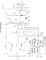
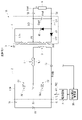
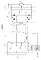
- FIG. 1 is a circuit diagram showing a schematic configuration example of a switching power supply device according to a first embodiment of the present invention
- FIG. 2 is a circuit diagram schematically showing an equivalent circuit of the switching power supply device shown in FIG. 1
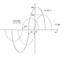
- FIG. FIG. 4 is a schematic diagram for explaining a current phase difference according to the first embodiment
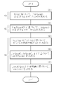
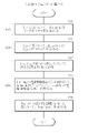
- FIG. 4 is a flow chart showing an example of a method for estimating load current according to the first embodiment
- FIG. 5 is a circuit diagram showing a schematic configuration example of a switching power supply device according to a second embodiment
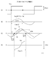
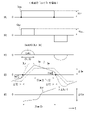
- FIG. 10 is a timing chart showing various waveform examples used in technique A according to the second embodiment
- FIG. 11 is a flow chart showing an example of a load current estimation method (method A) according to the second embodiment
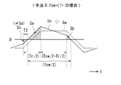
- FIG. 11 is a timing chart showing various waveform examples used in technique B according to the second embodiment;
- FIG. 9 is a schematic diagram for explaining the positive/negative asymmetry in the waveform example of the transformer exciting current shown in FIG. 8 ;
- FIG. 13 is a flow chart showing another example (method B) of the method of estimating the load current according to the second embodiment;
- FIG. 3 is a circuit diagram showing a schematic configuration example of a switching power supply device according to Modification 1;
- FIG. 10 is a flow chart showing an example of pre-correction processing according to Modification 1.
- FIG. 13 is a schematic diagram for explaining an example of the correction processing shown in FIG. 12;
- FIG. FIG. 11 is a circuit diagram showing a schematic configuration example of a switching power supply device according to Modification 2;
- FIG. 11 is a circuit diagram showing a schematic configuration example of a switching power supply device according to Modification 3;
- FIG. 11 is a circuit diagram showing a schematic configuration example of a switching power supply device according to
- FIG. 1 is a circuit diagram showing a schematic configuration example of a switching power supply (switching power supply 1) according to a first embodiment of the present invention.
- the switching power supply 1 functions as a DC-DC converter that converts a DC input voltage Vin supplied from a DC input power supply 10 (eg, a battery) into a DC output voltage Vout and supplies power to a load 9. .
- the load 9 may be, for example, an electronic device, a battery, or the like.
- the switching power supply device 1 is a so-called "(insulated half-bridge) LLC resonant type" DC-DC converter, as will be described below.
- the mode of voltage conversion in the switching power supply device 1 may be either up-conversion (boosting) or down-conversion (stepping down).
- the DC input voltage Vin corresponds to a specific example of "input voltage” in the present invention
- the DC output voltage Vout corresponds to a specific example of "output voltage” in the present invention
- the DC input power supply 10 corresponds to a specific example of the "power supply” in the present invention
- a system including the DC input power supply 10 and the switching power supply device 1 is a specific example of the "power supply system” in the present invention. corresponds to the example.
- the switching power supply device 1 includes two input terminals T1 and T2, two output terminals T3 and T4, an inverter circuit 2, a transformer 3, a rectifying/smoothing circuit 4, a drive circuit 5, and a load current estimator 6. It has A DC input voltage Vin is input between the input terminals T1 and T2, and a DC output voltage Vout is output between the output terminals T3 and T4.
- the input terminals T1 and T2 correspond to a specific example of "input terminal pair" in the present invention
- the output terminals T3 and T4 correspond to a specific example of "output terminal pair” in the present invention.
- An input capacitor may be arranged between the primary high-voltage line L1H connected to the input terminal T1 and the primary low-voltage line L1L connected to the input terminal T2. Specifically, at a position between the inverter circuit 2 and the input terminals T1 and T2, which will be described later, the first end (one end) of the input capacitor is connected to the primary side high voltage line L1H, and the second end of the input capacitor is connected to the primary side high voltage line L1H. The end (the other end) may be connected to the primary side low pressure line L1L.
- Such an input capacitor is a capacitor for stabilizing the DC input voltage Vin input from the input terminals T1 and T2.
- the inverter circuit 2 is arranged between the input terminals T1, T2 and a primary winding 31 of the transformer 3, which will be described later.
- the inverter circuit 2 has two switching elements S1 and S2, a resonant inductor Lr, and a resonant capacitor Cr, and is a so-called "half-bridge type" inverter circuit.
- the resonance inductor Lr may be configured by a leakage inductance in the transformer 3, which will be described later, or may be provided separately from such a leakage inductance.
- the primary side high pressure line L1H and the primary side low pressure line L1L each correspond to a specific example of "a pair of connection lines” in the present invention.
- the switching element S1 corresponds to a specific example of the "first switching element” in the present invention
- the switching element S2 corresponds to a specific example of the "second switching element” in the present invention.
- switching elements S1 and S2 switching elements such as a field effect transistor (MOS-FET; Metal Oxide Semiconductor-Field Effect Transistor) and an IGBT (Insulated Gate Bipolar Transistor) are used.
- MOS-FET Metal Oxide Semiconductor-Field Effect Transistor
- IGBT Insulated Gate Bipolar Transistor
- the switching elements S1 and S2 are each composed of a MOS-FET.
- the capacitors and diodes (not shown in FIG. 1) connected in parallel to the switching elements S1 and S2 are respectively connected to the MOS-FETs. It can consist of a parasitic capacitance of the FET or a parasitic diode.
- two switching elements S1 and S2 are connected in series in this order between the input terminals T1 and T2 (between the primary high voltage line L1H and the primary low voltage line L1L).
- the switching element S1 is arranged between the primary side high voltage line L1H and the connection point P1
- the switching element S2 is arranged between the connection point P1 and the primary side low voltage line L1L.
- the resonance inductor Lr and the resonance capacitor Cr in the inverter circuit 2 and the primary winding 31 in the transformer 3, which will be described later, are connected in series between the connection point P1 and the primary low-voltage line L1L. It is Specifically, in the example of FIG. 1, a first end (one end) of the resonance inductor Lr is connected to the connection point P1, and a second end (the other end) of the resonance inductor Lr is connected to the primary winding described above. 31 (connection point P3). The other end of the primary winding 31 is connected to a connection point P2 as the first end (one end) of the resonance capacitor Cr, and the second end (the other end) of the resonance capacitor Cr is connected to the primary side. It is connected to the low pressure line L1L. Incidentally, as shown in FIG. 1, the second end of this resonance capacitor Cr is connected to the ground GND via the primary side low voltage line L1L.
- connection point P1 described above corresponds to a specific example of "a connection point (a connection point between the first and second switching elements)" in the present invention.
- the switching elements S1 and S2 perform switching operations (on/off operations) in accordance with drive signals SG1 and SG2 supplied from the drive circuit 5, which will be described later. Become. That is, the DC input voltage Vin applied between the input terminals T1 and T2 is converted into AC voltage and output to the transformer 3 (primary winding 31).
- the transformer 3 has one primary winding 31 and two secondary windings 321 and 322 .
- connection point P3 of the primary winding 31 is connected to the other end of the resonance inductor Lr described above, and the other end of the primary winding 31 is connected to the resonance capacitor described above. Cr is connected to one end (connection point P2).
- a first end of the secondary winding 321 is connected to a cathode of the rectifier diode 41 described later via a connection line L21 described later, and a second end of the secondary winding 321 is connected. is connected to a center tap P6 in a rectifying/smoothing circuit 4 which will be described later.
- a first end of the secondary winding 322 is connected to a cathode of a rectifier diode 42 described later via a connection line L22 described later, and a second end of the secondary winding 322 is connected. is connected to the center tap P6. That is, the second ends of the secondary windings 321 and 322 are commonly connected to the center tap P6.
- the transformer 3 converts the voltage generated by the inverter circuit 2 (rectangular pulse wave voltage input to the primary winding 31 of the transformer 3), and the secondary windings 321 and 322 AC voltage is output from the end.
- the degree of voltage conversion of the DC output voltage Vout with respect to the DC input voltage Vin depends on the turns ratio between the primary winding 31 and the secondary windings 321 and 322 and the switching frequency fsw, which will be described later. , is determined.
- the rectifying/smoothing circuit 4 has two rectifying diodes 41 and 42 and one output smoothing capacitor Cout. Specifically, the rectifying/smoothing circuit 4 includes a rectifying circuit having rectifying diodes 41 and 42 and a smoothing circuit having an output smoothing capacitor Cout.
- the above rectifier circuit is a so-called "center tap type" rectifier circuit. That is, the anodes of the rectifier diodes 41 and 42 are respectively connected to the ground line LG, and the cathode of the rectifier diode 41 is connected to the aforementioned first end of the secondary winding 321 via the connection line L21 to The cathode of diode 42 is connected to the aforementioned first end of secondary winding 322 via connection line L22. Further, as described above, the second ends of the secondary windings 321 and 322 are commonly connected to the center tap P6, and the center tap P6 is connected via the output line LO. It is connected to the output terminal T3.
- the ground line LG described above is connected to the output terminal T4 described above.
- an output smoothing capacitor Cout is connected between the output line LO and the ground line LG (between the output terminals T3 and T4). That is, the first end of the output smoothing capacitor Cout is connected to the output line LO, and the second end of the output smoothing capacitor Cout is connected to the ground line LG.
- the rectifying circuit including the rectifying diodes 41 and 42 rectifies and outputs the AC voltage output from the transformer 3 .
- a smoothing circuit including an output smoothing capacitor Cout smoothes the voltage rectified by the rectifying circuit to generate a DC output voltage Vout. It should be noted that the DC output voltage Vout generated in this manner causes the load current Iout (DC output current) to flow to the load 9, and power is supplied to the load 9 from the output terminals T3 and T4. (See Figure 1).
- the drive circuit 5 is a circuit that performs switching drive for controlling the operations of the switching elements S1 and S2 in the inverter circuit 2, respectively. Specifically, the drive circuit 5 controls switching operations (ON/OFF operations) of the switching elements S1 and S2 by supplying the driving signals SG1 and SG2 to the switching elements S1 and S2, respectively. It is designed to
- the drive circuit 5 performs frequency control when controlling switching operations of the switching elements S1 and S2 (performing switching driving). That is, PFM (Pulse Frequency Modulation) control is performed in the drive signals SG1 and SG2.
- PFM Pulse Frequency Modulation
- the drive circuit 5 performs the above-described switching drive so that the switching elements S1 and S2 operate at fixed duty ratios although the switching frequencies fsw of the switching elements S1 and S2 vary. ing.
- Ton1 and Ton2 the on-periods of the switching elements S1 and S2 are expressed as Ton1 and Ton2, respectively.
- the drive circuit 5 performs switching driving using an estimated value of the load current Iout (load current estimated value Iout(est) described later) obtained by the load current estimator 6 described below. is to be performed. Specifically, the drive circuit 5 controls the value of the load current Iout within an appropriate range by performing switching drive using the load current estimated value Iout(est).
- the load current estimator 6 estimates the load current Iout described above (determines the load current estimated value Iout(est) by a method described later). Specifically, although the details will be described later, the load current estimator 6 calculates the load current Iout based on the resonant inductor current ILr flowing through the resonant inductor Lr and the transformer exciting current Im flowing through the primary winding 31. Obtain the primary side conversion value IoutAC. Then, the load current estimator 6 obtains the load current estimated value Iout(est) based on this primary side conversion value IoutAC.
- the load current estimator 6 utilizes the current phase difference ⁇ 1 between the resonant inductor current ILr and the transformer excitation current Im to obtain the load current estimated value Iout(est) is obtained. Specifically, the load current estimator 6 calculates such a current potential based on the voltage Vcr across the resonant capacitor Cr and the voltage Vnp across the primary winding 31, which will be described below. Phase difference ⁇ 1 is obtained.
- Such a load current estimator 6 has two detectors 61 and 62 and a controller 60 in the example shown in FIG.
- the detection unit 61 is connected between both ends of the resonance capacitor Cr (as shown in FIG. 1, when the second end of the resonance capacitor Cr is connected to the common ground GND with the detection unit 61, the connection point P2 and This circuit detects the voltage Vcr between the primary side low voltage line L1L). Although the details will be described later, the detection unit 61 also performs predetermined arithmetic processing based on the voltage Vcr thus detected.
- the detection unit 62 is a circuit that detects the voltage Vnp across the primary winding 31 (between the connection points P2 and P3 shown in FIG. 1). Although the details will be described later, the detection unit 62 also performs predetermined arithmetic processing based on the voltage Vnp thus detected.
- the control unit 60 is a circuit that obtains the load current estimated value Iout(est) by performing a predetermined arithmetic process, which will be described later, based on the above arithmetic processing results in the detection parts 61 and 62 . Further, the control unit 60 uses the load current estimated value Iout(est) thus obtained to control the switching drive in the drive circuit 5 (controls the switching operations of the switching elements S1 and S2). It's like Specifically, although the details will be described later, the control unit 60 performs such a control based on the voltage Vcr across the resonance capacitor Cr and the voltage Vnp across the primary winding 31 . control switching operation. As a result, as described above, the value of the load current Iout is controlled within an appropriate range.
- the AC voltage (transformed AC voltage described above) output from the transformer 3 is rectified by the rectifying diodes 41 and 42 in the rectifying circuit, and then is rectified by the output smoothing capacitor Cout in the smoothing circuit. smoothed.
- the DC output voltage Vout is output from the output terminals T3 and T4. This DC output voltage Vout causes a load current Iout to flow to the load 9 and power to be supplied to the load 9 .
- FIG. 2 is a schematic circuit diagram showing an equivalent circuit of the switching power supply device 1 shown in FIG. 1 (an equivalent circuit of the LLC resonance type converter described above).
- VinAC is the AC input voltage
- Lm is the exciting inductance value of the transformer 3
- RL(AC) is the primary side load
- n is the primary side winding 31 and the secondary side winding.
- the resistance value of the primary side load RL(AC) is expressed as (8 ⁇ n 2 ⁇ RL)/ ⁇ 2 using the turns ratio n and the resistance value RL of the load 9 described above.
- FHA Fundamental wave approximation method
- FIG. 3 is a schematic diagram for explaining the above-described current phase difference ⁇ 1 according to the present embodiment.
- current phase difference ⁇ 1 between current i1 (resonant inductor current ILr) and current i2 (transformer excitation current Im), and current i2 and current i (primary side conversion value of load current Iout The current phase difference ⁇ 3 with IoutAC) is also shown.
- i2 Im2 ⁇ sin ⁇ t (2) (Im1, Im2: amplitude value, ⁇ : angular frequency, t: time)
- A Im1*cos ⁇ 1-Im2 (5)
- B Im1 ⁇ sin ⁇ 1 (6)
- a 2 +B 2 ) 1/2 (Im1 2 +Im2 2 -2.Im1.Im2.cos ⁇ 1) 1/2 ... (7)
- ⁇ 3 tan ⁇ 1 (B/A) (8)
- the currents i1, i2, and i are converted to primary-side conversion values of the resonant inductor current ILr, the transformer excitation current Im, and the load current Iout, respectively, as described above.
- IoutAC When replaced as IoutAC, it becomes as follows. That is, ILr(peak), Im(peak), and IoutAC(peak) as these peak values are respectively represented by the following equations (9) to (12) (see also each parameter in FIG. 2). .
- the load current Iout is estimated using such a calculation method.
- FIG. 4 is a flow chart showing an example of a method for estimating the load current Iout by the load current estimator 6 according to the present embodiment.
- this estimation method first, based on the voltage Vcr (see FIG. 1) across the resonance capacitor Cr detected by the detection unit 61 as described above, ILr(peak) and this voltage Vcr , and the zero-crossing points of , respectively (step S11 in FIG. 4). Specifically, the detection unit 61 obtains ILr(peak) based on the voltage Vcr using the above equation (9).
- step S12 based on the voltage Vnp across the primary winding 31 (see FIG. 1: corresponding to VoutAC in FIG. 2) detected by the detection unit 62 as described above, Im(peak) and this A zero crossing point of the voltage Vnp is obtained (step S12). Specifically, the detection unit 62 obtains Im(peak) based on the voltage Vnp using the above equations (10) and (11).
- control unit 60 controls the current phase difference ⁇ 1 between the resonant inductor current ILr and the transformer excitation current Im (see FIG. 2) based on the zero crossing points of the voltage Vcr and the voltage Vnp obtained by the detection units 61 and 62. is obtained (step S13). Specifically, the control unit 60 obtains such a current phase difference ⁇ 1 from the difference between these zero cross points.
- control unit 60 calculates the peak value of the primary side conversion value IoutAC of the load current Iout using the above equation (12). A value (IoutAC(peak)) is obtained (step S14).
- the control unit 60 in the load current estimating unit 6 controls the voltage Vcr across the resonance capacitor Cr and the voltage Vcr across the primary winding 31 .
- the switching operation is controlled based on the voltage Vnp in between.
- the load current estimator 6 obtains the primary side conversion value IoutAC of the load current Iout based on the resonant inductor current ILr and the transformer exciting current Im, and calculates the primary side conversion value IoutAC.
- a load current estimated value Iout(est) is obtained based on the value IoutAC.
- the control unit 60 controls the value of the load current Iout by performing switching control using the load current estimated value Iout(est) obtained in this way.
- the load current estimated value Iout(est) is obtained based on the primary side conversion value IoutAC of the load current Iout obtained without using a current sensor such as a resistive element on the primary side.
- the value of the load current Iout is controlled based on the estimated current value Iout(est).
- the load current Iout is set to 10 [% ] can be estimated within the error.
- the present embodiment it is possible to reduce the size of the switching power supply 1 compared to the above-described general LLC resonance type switching power supply.
- the current phase difference ⁇ 1 between the resonant inductor current ILr and the transformer excitation current Im is used to determine the load current estimated value Iout(est). can be easily performed.
- the current phase difference ⁇ 1 is obtained based on the voltage Vcr across the resonant capacitor Cr and the voltage Vnp across the primary winding 31. Therefore, the load current Iout can be estimated more easily.
- the resonance inductor Lr in the inverter circuit 2 is constituted by the leakage inductance in the transformer 3, it is not necessary to provide the resonance inductor Lr separately. can be reduced. As a result, it is possible to further reduce the size and cost of the switching power supply device 1 .
- the switching elements S1 and S2 in the inverter circuit 2 are configured by MOS-FETs, respectively, so that the switching frequency fsw can be increased and the size of parts can be reduced. It becomes possible.
- the rectifier circuit in the rectifying/smoothing circuit 4 is a so-called "center tap type" rectifying circuit. Compared with the case, it is as follows. That is, the number of rectifying elements is reduced to two (rectifying diodes 41 and 42), and as a result, it is possible to reduce the size, loss, and cost of the rectifying circuit.
- FIG. 5 is a circuit diagram showing a schematic configuration example of a switching power supply (switching power supply 1A) according to the second embodiment.
- a system including the DC input power supply 10 and the switching power supply device 1A corresponds to a specific example of the "power supply system" of the present invention.
- the switching power supply 1A of the second embodiment corresponds to the switching power supply 1 of the first embodiment provided with a load current estimating section 6A instead of the load current estimating section 6. , and other configurations are the same.
- the load current estimator 6A estimates the load current Iout (determines the load current estimated value Iout(est)). Similarly to the load current estimating section 6, the load current estimating section 6A also obtains the primary side conversion value IoutAC of the load current Iout based on the resonant inductor current ILr and the transformer exciting current Im. Like the load current estimating section 6, the load current estimating section 6A also obtains the load current estimated value Iout(est) based on the primary side conversion value IoutAC.
- the load current estimator 6A calculates the current-time product (integral value of the current along the time axis) between the resonant inductor current ILr and the transformer excitation current Im, although the details will be described later. : corresponding to the amount of charge) is used to obtain the load current estimated value Iout(est). Further, the load current estimator 6A, which will be described later in detail, determines whether the switching frequency fsw in the switching elements S1 and S2 and the resonance frequency fr in the resonance operation using the resonance inductor Lr and the resonance capacitor Cr are large or small. The method of estimating the load current Iout using such a difference in the current-time product is changed according to the relationship.
- Such a load current estimator 6A has three detectors 61A, 62A, 63A and a controller 60A in the example shown in FIG.
- the detection section 61A is a circuit that detects the voltage Vcr across the resonance capacitor Cr. Although the details will be described later, the detection section 61A also performs predetermined arithmetic processing based on the voltage Vcr thus detected.
- the detection section 62A is a circuit that detects the voltage Vnp across the primary winding 31, similar to the detection section 62. Although the details will be described later, the detection section 62A also performs predetermined arithmetic processing based on the voltage Vnp thus detected.
- the detection unit 63A is a circuit that detects the switching voltage Vsw corresponding to the potential of the connection point P1. Although the details will be described later, the detection section 63A also performs predetermined arithmetic processing based on the switching voltage Vsw thus detected.
- the detection section 63A is connected to the ground (ground GND) common to the detection section 61A and the second end side of the resonance capacitor Cr.
- the detector 63A is arranged between the primary low-pressure line L1L and the connection point P1. You may make it arrange
- the control unit 60A is a circuit that obtains the load current estimated value Iout(est) through a predetermined arithmetic process described later based on the above-described arithmetic processing results of the detection units 61A, 62A, and 63A. Further, like the control unit 60, the control unit 60A controls the switching drive in the drive circuit 5 based on the load current estimated value Iout(est) obtained in this manner. As a result, as described above, the drive circuit 5 controls the value of the load current Iout to be within an appropriate range.
- FIG. 6 is a timing chart showing examples of various waveforms used in the method A (method when fsw>fr) according to the present embodiment.
- FIG. 6(A) is the voltage Vnp
- FIG. 6(C) is the resonant inductor current ILr
- FIG. 6D shows waveform examples of the transformer exciting current Im and the voltage Vcr. Note that the horizontal axis indicates time t, and the same applies to subsequent timing charts.
- FIG. 7 is a flow chart showing an example of the method of estimating the load current Iout (method A described above) by the load current estimator 6A according to the present embodiment.
- the load current estimator 6A calculates the voltage Vcr across the resonance capacitor Cr and the voltage Vnp across the primary winding 31 as described below. , the load current Iout is estimated using the aforementioned difference in the current-time product. That is, in method A, the load current estimator 6A uses only the detection results of the detectors 61A and 62A, and does not use the detection result of the detector 63A.
- this method A first, based on the voltage Vcr (see FIGS. 5 and 6D) detected by the detection unit 61A as described above, the resonant inductor current ILr and this resonant inductor current The zero cross points of ILr are obtained (step S21 in FIG. 7). Specifically, the detection unit 61A obtains the resonant inductor current ILr by performing a differential operation on the voltage Vcr.
- control unit 60A obtains the delay time ⁇ T1 (see FIG. 6(C)) based on the zero crossing points of the resonant inductor current ILr and the voltage Vnp obtained by the detection units 61A and 62A (step S23). Specifically, as shown in FIG. 6, control unit 60A obtains such delay time ⁇ T1 from the time difference between the zero crossing points of resonant inductor current ILr and voltage Vnp.
- (a+b) is obtained (step S24: see FIG. 6B).
- the control unit 60A obtains such a current-time product (a+b) using the following equation (15) based on the variation ⁇ Im of the transformer exciting current Im and the delay time ⁇ T1.
- the current-time products a and b are shown in FIG. 6(C), respectively.
- (a+b) (Cr ⁇ Vcr) ⁇ ( ⁇ Im ⁇ T1)
- FIG. 8 is a timing chart showing examples of various waveforms used in method B (method when fsw ⁇ fr) according to the present embodiment.
- FIG. 8(A) is the switching voltage Vsw
- FIG. 8(B) is the voltage Vnp
- FIG. 8(C) is the primary side conversion value IoutAC of the load current Iout
- FIG. 8(D) is the resonance inductor
- FIG. 8(E) shows examples of waveforms of the current ILr, the transformer excitation current Im, and the voltage Vcr.
- FIG. 9 is a schematic diagram for explaining the positive/negative asymmetry (asymmetry of positive/negative values) in the waveform example of the transformer exciting current Im shown in FIG. ). Specifically, in FIG. 9 (and FIG. 8(D)), regarding the waveform change (approximate waveform adjustment) for compensating for such positive/negative asymmetry, the transformer exciting current Im (indicated by a dashed line) and the transformer excitation current Im after the waveform change (indicated by a solid line).
- the load current estimator 6A estimates the load current Iout in consideration of the positive/negative asymmetry in the transformer exciting current Im. Specifically, for example, in the case of (Sa ⁇ Sb) and (fsw ⁇ fr) like the integrated values Sa and Sb shown in FIG. , the positive and negative values are asymmetric. When the transformer excitation current Im is positive and negative asymmetrically, the positive and negative cannot be canceled, so even if the detected value is integrated, the load current Iout cannot be separated. Therefore, in this method B, as described above, the waveform change (approximate waveform adjustment) is applied to compensate for the positive/negative asymmetry in the transformer exciting current Im (Fig. 8(D), Fig. See arrow for Im shown in 9).
- FIG. 10 is a flow chart showing an example of the method of estimating the load current Iout by the load current estimating unit 6A (method B described above) according to the present embodiment.
- the load current estimator 6A calculates the current time
- the load current Iout is estimated using the product difference. That is, in this method B, unlike the method A described above, the load current estimating unit 6A uses the detection results of the detecting units 61A, 62A, and 63A described above.
- step S21 the processing of step S21 is performed in the same manner as in the case of method A described above. That is, based on the voltage Vcr (see FIGS. 5 and 8E) detected by the detection unit 61A as described above, the resonant inductor current ILr and the zero cross point of the resonant inductor current ILr are obtained ( Step S21 in FIG. 10). Specifically, the detection unit 61A obtains the resonant inductor current ILr by performing a differential operation on the voltage Vcr.
- the change amount ⁇ Im (see FIG. 8D) of the transformer exciting current Im is obtained (step S32).
- the detection unit 63A obtains the zero-cross point of the switching voltage Vsw (step S33).
- control unit 60A obtains the delay time ⁇ T2 (see FIG. 8(D)) based on the zero-crossing points of the resonant inductor current ILr and the switching voltage Vsw obtained by the detection units 61A and 63A (step S34). . Specifically, as shown in FIG. 8, control unit 60A obtains such delay time ⁇ T2 from the time difference between the zero crossing points of resonant inductor current ILr and switching voltage Vsw.
- the load current estimated value Iout(est) is obtained by using the difference in current-time product between the resonant inductor current ILr and the transformer excitation current Im. can be easily estimated.
- the method of estimating the load current Iout using the difference in the current-time product is changed according to the magnitude relationship between the switching frequency fsw and the resonance frequency fr. Specifically, when the switching frequency fsw is higher than the resonance frequency fr, the load current estimation unit 6A sets the voltage Vcr across the resonance capacitor Cr and the voltage Vnp across the primary winding 31 to , the load current Iout is estimated using the difference in the current-time product. Conversely, when the switching frequency fsw is lower than the resonance frequency fr, the load current estimator 6A calculates the current-time product based on the voltage Vcr and the voltage Vnp and the switching voltage Vsw described above. The load current Iout is estimated using the difference. Accordingly, in the present embodiment, it is possible to select an appropriate estimation method according to such a magnitude relationship between frequencies, so that it is possible to improve the accuracy of estimating the load current Iout.
- the load current Iout is estimated as follows. That is, even in such a case of (fsw ⁇ fr) (as described above, in the case of the operation mode in which the primary side conversion value IoutAC of the load current Iout is discontinuous), the load current Iout can be estimated with high accuracy. Therefore, it is possible to further improve the estimation accuracy of the load current Iout.
- the load current Iout could be estimated with the following error. ⁇ When (fsw>fr) (in the case of operation mode in which resonant inductor current ILr is continuous): Error within about 5 [%] ⁇ When (fsw ⁇ fr) (when resonant inductor current ILr is discontinuous mode): Error within about 10 [%]
- FIG. 11 is a circuit diagram showing a schematic configuration example of a switching power supply (switching power supply 1B) according to Modification 1. As shown in FIG.
- a system including the DC input power supply 10 and the switching power supply device 1B corresponds to a specific example of the "power supply system" of the present invention.
- a switching power supply device 1B of this modified example 1 is provided with a load current estimating section 6B described below instead of the load current estimating sections 6 and 6A in the switching power supply devices 1 and 1A of the first and second embodiments. , and other configurations are the same.
- the load current estimator 6B basically estimates the load current Iout in the same manner as the load current estimator 6 or the load current estimator 6A described above. However, as described below, the load current estimator 6B further includes a predetermined value corrected in advance according to the measured value of the correspondence (output characteristics) between the load current Iout and the DC output voltage Vout. parameters (described later) are used to estimate the load current Iout.
- Such pre-correction processing for predetermined parameters is performed in advance, for example, when the switching power supply device 1B is inspected before product shipment.
- the predetermined parameter is set to a value after such pre-correction processing (a value finely adjusted on calculation). This is because the estimated value of the load current Iout (load current estimated value Iout(est)) may fluctuate due to individual variations in each element in the switching power supply device 1B.
- the above-described predetermined parameters include, for example, the capacitance value of the resonant capacitor Cr, the exciting inductance value Lm of the transformer 3, and the load current estimator 6B (each of the detectors 61, 62, 61A, 62A, and 63A described above). and the like.
- FIG. 12 is a flow chart showing an example of the above-described pre-correction processing according to Modification 1.
- FIG. 13 is a schematic diagram for explaining an example of the correction processing shown in FIG. Specifically, FIG. 13 shows an example of the output characteristics (correspondence between the load current Iout and the DC output voltage Vout at the time of overcurrent droop) in the switching power supply device 1B. It is shown as 100%.
- load current estimated value Iout(est) is reduced.
- Correction is performed (step S43). Specifically, correction is performed to reduce the above-described predetermined parameters (for example, the capacitance value of the resonance capacitor Cr, the exciting inductance value Lm of the transformer 3, etc.). After step S43, the process returns to step S41.
- load current estimated value Iout(est) is increased.
- Correction is performed (step S46). Specifically, correction is performed to increase the above-described predetermined parameters (for example, the capacitance value of the resonance capacitor Cr, the exciting inductance value Lm of the transformer 3, etc.). After step S46, the process returns to step S44.
- the load current Iout is estimated using a predetermined parameter corrected in advance according to the measured value of the correspondence between the load current Iout and the DC output voltage Vout. So it looks like this: That is, for example, when the switching power supply device 1B is inspected at the time of product shipment or the like, such a preliminary correction is performed. , and the manufacturing yield can be improved. As a result, it is also possible to further reduce the cost of the switching power supply device 1B.
- FIG. 14 is a circuit diagram showing a schematic configuration example of a switching power supply (switching power supply 1C) according to Modification 2. As shown in FIG.
- a system including the DC input power supply 10 and the switching power supply device 1C corresponds to a specific example of the "power supply system" of the present invention. .
- the switching power supply device 1C of Modification 2 has a transformer 3C and a rectification/smoothing circuit 4C instead of the transformer 3 and the rectification/smoothing circuit 4 in the switching power supply devices 1, 1A, and 1B described thus far. They correspond, and other configurations are the same.
- the transformer 3C has one primary winding 31 and one secondary winding 32. That is, the transformer 3 is provided with two secondary windings 321 and 322, whereas the transformer 3C is provided with only one secondary winding 32.
- FIG. The secondary winding 32 has a first end connected to a connection point P7 in the rectification/smoothing circuit 4C, which will be described later, and a second end connected to a connection point P8 in the rectification/smoothing circuit 4C.
- the transformer 3C also converts the voltage (rectangular pulse wave voltage) generated by the inverter circuit 2 and outputs an AC voltage from the end of the secondary winding 32.
- the degree of voltage conversion of the DC output voltage Vout with respect to the DC input voltage Vin is determined by the turns ratio between the primary winding 31 and the secondary winding 32 and the switching frequency fsw described above. .
- the rectifying/smoothing circuit 4C has four rectifying diodes 41 to 44 and one output smoothing capacitor Cout. Specifically, the rectifying/smoothing circuit 4C includes a rectifying circuit having rectifying diodes 41 to 44 and a smoothing circuit having an output smoothing capacitor Cout. In other words, the rectifying/smoothing circuit 4C is obtained by changing the configuration of the rectifying circuit in the rectifying/smoothing circuit 4. FIG.
- rectifying diodes 41 to 44 correspond to a specific example of "plurality of rectifying elements" in the present invention.
- the rectifier circuit of Modification 2 is a so-called “bridge type” rectifier circuit, unlike the rectifier circuits of the first and second embodiments and Modification 1 (so-called “center tap type” rectifier circuits). ing. That is, the cathodes of rectifier diodes 41 and 43 are connected to output line LO, respectively, and the anode of rectifier diode 41 is connected to the cathode of rectifier diode 42 and the first end of secondary winding 32 at connection point P7. It is connected.
- the anodes of the rectifier diodes 42 and 44 are connected to the ground line LG, respectively, and the cathode of the rectifier diode 44 is connected to the anode of the rectifier diode 43 and the second end of the secondary winding 32 at the connection point P8. It is connected.
- the rectifying circuit 4C having such a configuration, as in the rectifying/smoothing circuit 4, the rectifying circuit including the rectifying diodes 41 to 44 rectifies and outputs the AC voltage output from the transformer 3C. It's becoming
- the rectifier circuit in the rectifying/smoothing circuit 4C is a bridge type rectifying circuit.
- the number of windings (the number of secondary windings) is reduced to one (secondary winding 32). As a result, it is possible to reduce the size and loss of the transformer 3C.
- Modifications 3 and 4 (Constitution)
- the switching power supply devices according to Modifications 3 and 4 are similar to the first and second embodiments, Modification 1, and Modification 2 described above, respectively.
- Each of the rectifying circuits in the circuits 4 and 4C is a so-called synchronous rectifying circuit as described below.
- FIG. 15 is a circuit diagram showing a schematic configuration example of a switching power supply (switching power supply 1D) according to Modification 3. As shown in FIG.
- the switching power supply device 1D of this modified example 3 is provided with a rectifying/smoothing circuit 4D instead of the rectifying/smoothing circuit 4 in the switching power supply devices 1, 1A, and 1B of the first and second embodiments and the first modification. , and other configurations are the same.
- the rectification diodes 41 and 42 described above are respectively configured by MOS-FETs (MOS transistors M9 and M10) as switching elements. It is In this synchronous rectification circuit, the MOS transistors M9 and M10 themselves are controlled to be turned on (perform synchronous rectification) in synchronization with the period during which the parasitic diodes of the MOS transistors M9 and M10 are conducting. be.
- the drive circuit 5 of Modification 4 uses the drive signals SG9 and SG10 to control the ON/OFF operations of the MOS transistors M9 and M10 (see FIG. 15).
- FIG. 16 is a circuit diagram showing a schematic configuration example of a switching power supply (switching power supply 1E) according to Modification 4. As shown in FIG.
- the switching power supply device 1E of Modification 4 corresponds to the switching power supply device 1C of Modification 2 in which a rectifying/smoothing circuit 4E is provided instead of the rectifying/smoothing circuit 4C, and other configurations are the same. ing.
- the MOS transistors M11 to M14 are synchronized with the period during which the parasitic diodes of the MOS transistors M11 to M14 are conductive. M14 itself is also controlled to be on (perform synchronous rectification).
- the drive circuit 5 of Modification 4 uses the drive signals SG11 to SG14 to control the ON/OFF operations of the MOS transistors M11 to M14 (see FIG. 16).
- a system including the DC input power supply 10 and the switching power supply 1D or switching power supply 1E is one of the "power supply systems" in the present invention. Corresponds to specific examples.
- a plurality of rectifying elements in the rectifying circuit are each composed of a switching element, and the rectifying circuit is a synchronous rectifying circuit.
- a synchronous rectification circuit reduces the conduction loss during rectification, so that it is possible to reduce the size and loss of the rectification circuit.
- MOS-FET MOS-FET
- HEMT High Electron Mobility Transistor
- HFET Heterostructure Field-Effect Transistor
- the configuration of the inverter circuit was specifically described, but it is not limited to the examples of the above embodiments and the like. good too.
- the arrangement relationship among the resonant inductor Lr, the resonant capacitor Cr, and the primary winding 31, which are connected in series with each other is not limited to the arrangement relationship described in the embodiment and the like. The order may be random.
- the resonance inductor Lr, the resonance capacitor Cr, and the primary winding 31 are arranged between the connection point P1 and the primary low-voltage line L1L (input terminal T2).
- transformer primary winding and secondary winding
- Primary winding and secondary winding may have other configurations.
- rectifying and smoothing circuit (rectifying circuit and smoothing circuit) was specifically described, but it is not limited to the examples of the above-described embodiments and the like.
- a rectifying circuit and a smoothing circuit may have other configurations.
- the method of controlling the operation of each switching element (switching drive) by the drive circuit has been specifically described. You may make it use another method as a method of .
- the method for estimating the load current Iout described above is not limited to the method described in the above embodiment and the like, and other methods may be used.
- the configuration of the load current estimating section was specifically described. Other configurations may be used as the detection unit and the control unit).
- the DC-DC converter was described as an example of the switching power supply device according to the present invention, but the present invention is applicable to other types of switching power supply devices such as AC-DC converters. It can also be applied to
Landscapes
- Engineering & Computer Science (AREA)
- Power Engineering (AREA)
- Dc-Dc Converters (AREA)
Abstract
Description
1.第1の実施の形態(電流位相差を利用して負荷電流を推定する場合の例)
2.第2の実施の形態(電流時間積の差を利用して負荷電流を推定する場合の例)
3.変形例
変形例1(所定のパラメータに関する事前の補正処理を行う場合の例)
変形例2(ブリッジ型の整流回路を用いた場合の例)
変形例3,4(同期整流回路とした場合の例)
4.その他の変形例
[構成]
図1は、本発明の第1の実施の形態に係るスイッチング電源装置(スイッチング電源装置1)の概略構成例を、回路図で表したものである。このスイッチング電源装置1は、直流入力電源10(例えばバッテリ)から供給される直流入力電圧Vinを直流出力電圧Voutに電圧変換し、負荷9に電力を供給するDC-DCコンバータとして機能するものである。なお、この負荷9としては、例えば電子機器やバッテリ等が挙げられる。また、このスイッチング電源装置1は、以下説明するように、いわゆる「(絶縁型ハーフブリッジ)LLC共振型」のDC-DCコンバータとなっている。なお、スイッチング電源装置1における電圧変換の態様としては、アップコンバート(昇圧)およびダウンコンバート(降圧)のいずれであってもよい。
インバータ回路2は、入力端子T1,T2と、後述するトランス3における1次側巻線31との間に、配置されている。このインバータ回路2は、2つのスイッチング素子S1,S2と、共振インダクタLrと、共振コンデンサCrとを有しており、いわゆる「ハーフブリッジ型」のインバータ回路となっている。なお、共振インダクタLrは、後述するトランス3における漏れインダクタンスにより構成されていてもよいし、あるいは、そのような漏れインダクタンスとは別個に設けられているようにしてもよい。
トランス3は、1つの1次側巻線31と、2つの2次側巻線321,322とを有している。
整流平滑回路4は、2個の整流ダイオード41,42と、1個の出力平滑コンデンサCoutとを有している。具体的には、この整流平滑回路4は、整流ダイオード41,42を有する整流回路と、出力平滑コンデンサCoutを有する平滑回路と、を含んでいる。
駆動回路5は、インバータ回路2におけるスイッチング素子S1,S2の動作をそれぞれ制御する、スイッチング駆動を行う回路である。具体的には、駆動回路5は、スイッチング素子S1,S2に対してそれぞれ、駆動信号SG1,SG2を個別に供給することで、各スイッチング素子S1,S2におけるスイッチング動作(オン・オフ動作)を制御するようになっている。
負荷電流推定部6は、前述した負荷電流Ioutの推定を行う(負荷電流推定値Iout(est)を、後述する手法にて求める)ものである。具体的には、詳細は後述するが、負荷電流推定部6は、共振インダクタLrに流れる共振インダクタ電流ILrと、1次側巻線31に流れるトランス励磁電流Imとに基づいて、負荷電流Ioutの1次側換算値IoutACを求める。そして、負荷電流推定部6は、この1次側換算値IoutACに基づいて、負荷電流推定値Iout(est)を求めるようになっている。
(A.基本動作)
このスイッチング電源装置1では、インバータ回路2において、直流入力電源10から入力端子T1,T2を介して供給される直流入力電圧Vinが、スイッチング素子S1,S2によってスイッチングされることで、矩形パルス波化した電圧が生成される。この矩形パルス波化した電圧は、トランス3における1次側巻線31へと供給され、このトランス3において変圧されることで、2次側巻線321,322から、変圧された交流電圧が出力される。
続いて、図1に加えて図2~図4を参照して、負荷電流推定部6における前述した負荷電流Ioutの推定動作(前述した負荷電流推定値Iout(est)を導出する動作)について、詳細に説明する。
図2は、図1に示したスイッチング電源装置1の等価回路(前述したLLC共振型のコンバータの等価回路)を、模式的に回路図で表したものである。なお、この図2中において、VinACは交流入力電圧を、Lmはトランス3の励磁インダクタンス値を、RL(AC)は1次側負荷を、nは1次側巻線31と2次側巻線321,322との巻数比(=1次側巻線31の巻数np/2次側巻線321,322の巻数ns)を、それぞれ示している。また、1次側負荷RL(AC)の抵抗値は、上記した巻数比nおよび負荷9の抵抗値RLを用いて、(8・n2・RL)/π2として表される。なお、このような手法は、基本波近似法(FHA:First Harmonic Approximation)と呼ばれており、矩形波電圧の基本周波数のみに注目して近似的に解析する手法となっている。
=Im1・sinωt・cоsφ1+Im1・cоsωt・sinφ1 …(1)
i2=Im2・sinωt …(2)
(Im1,Im2:振幅値、ω:角周波数、t:時間)
i(=i1-i2)=A・sinωt+B・cоsωt …(3)
=(A2+B2)1/2・sin(ωt+φ3) …(4)
A=Im1・cоsφ1-Im2 …(5)
B=Im1・sinφ1 …(6)
(A2+B2)1/2=(Im12+Im22-2・Im1・Im2・cоsφ1)1/2
…(7)
φ3=tan-1(B/A) …(8)
(Cr:共振コンデンサCrの容量値、Vcr(peak):電圧Vcrのピーク値)
Im(peak)=VoutAC/(ω・Lm)
=(4・n・Vout)/(π・ω・Lm) …(10)
VoutAC=(4/π)・n・Vout・sinωt …(11)
IoutAC(peak)=
(ILr(peak)2+Im(peak)2-2・ILr(peak)・Im(peak)・cоsφ1)1/2 …(12)
図4は、本実施の形態に係る、負荷電流推定部6による負荷電流Ioutの推定手法の一例を、流れ図で表したものである。
Iout(est)=n・(2/π)・IoutAC(peak) …(13)
ところで、LLC共振型のスイッチング電源装置では一般に、負荷電流についての過電流保護の際に、定電流垂下特性を実現するために、負荷電流の値を正確に検出する必要がある。
続いて、本発明の第2の実施の形態について説明する。なお、以下では、上記第1の実施の形態における構成要素と同一のものには同一の符号を付し、適宜説明を省略する。
図5は、第2の実施の形態に係るスイッチング電源装置(スイッチング電源装置1A)の概略構成例を、回路図で表したものである。
負荷電流推定部6Aは、負荷電流推定部6と同様に、負荷電流Ioutの推定を行う(負荷電流推定値Iout(est)を求める)ものである。また、この負荷電流推定部6Aも負荷電流推定部6と同様に、共振インダクタ電流ILrとトランス励磁電流Imとに基づいて、負荷電流Ioutの1次側換算値IoutACを求める。そして、この負荷電流推定部6Aも負荷電流推定部6と同様に、この1次側換算値IoutACに基づいて、負荷電流推定値Iout(est)を求めるようになっている。
(A.負荷電流Ioutの推定動作)
続いて、図5に加えて図6~図10を参照して、負荷電流推定部6Aにおける負荷電流Ioutの推定動作(負荷電流推定値Iout(est)を導出する動作)について、詳細に説明する。具体的には、以下では、前述したスイッチング周波数fswが前述した共振周波数frよりも高い場合(fsw>fr)の推定手法(手法A)と、逆に、スイッチング周波数fswが共振周波数frよりも低い場合(fsw<fr)の推定手法(手法B)とに分けて、詳細に説明する。
図6は、本実施の形態に係る上記した手法A(fsw>frの場合の手法)において利用される、各種波形例をタイミング図で表したものである。具体的には、図6(A)は電圧Vnp、図6(B)は、負荷電流Ioutの1次側換算値IoutAC(=ILr-Im)、図6(C)は、共振インダクタ電流ILrおよびトランス励磁電流Im、図6(D)は電圧Vcrについて、各波形例を示している。なお、横軸は時間tを示しており、以降のタイミング図においても同様である。
ΔIm=(Vnp・Tsw)/(4・Lm) …(14)
(Tsw:スイッチング周期(図6参照)、Lm:トランス3の励磁インダクタンス値)
(a+b)=(Cr・ΔVcr)-(ΔIm・ΔT1) …(15)
(Cr:共振コンデンサCrの容量値、ΔVcr:電圧Vcrの最大値と最小値との差(図6(D)参照))
Iout(est)=(n・(a+b))/(Tsw/2) …(16)
(n=np/ns:1次側巻線31と2次側巻線321,322との巻数比)
図8は、本実施の形態に係る上記した手法B(fsw<frの場合の手法)において利用される、各種波形例をタイミング図で表したものである。具体的には、図8(A)はスイッチング電圧Vsw、図8(B)は電圧Vnp、図8(C)は負荷電流Ioutの1次側換算値IoutAC、図8(D)は、共振インダクタ電流ILrおよびトランス励磁電流Im、図8(E)は電圧Vcrについて、各波形例を示している。
ΔIm=(Vnp・Tr)/(4・Lm) …(17)
(Tr:共振周期(=1/fr:図8,図9参照))
=Cr・(ΔVcr-2・ΔVcr1)-(ΔIm・Tsw-Im2・Tr)/2
=Cr・ΔVcr-(ΔIm・Tsw)/2+Im2・(Tr-2・ΔT2)/2 …(18)
Im2=(2・Cr・ΔVcr1)/ΔT2 …(19)
(ΔVcr1:電圧Vcrの遅れ時間ΔT2での変化量(図8(E)参照))
ップS36)。具体的には、制御部60Aは、以下の(20)式を用いて、負荷電流推定値Iout(est)を求める。
Iout(est)=(n・(a+b))/(Tsw/2) …(20)
このような本実施の形態のスイッチング電源装置1Aにおいても、基本的には、第1の実施の形態のスイッチング電源装置1と同様の作用により、同様の効果を得ることが可能である。
・(fsw>fr)の場合(共振インダクタ電流ILrが連続となる動作モードの場合):5[%]程度以内の誤差
・(fsw<fr)の場合(共振インダクタ電流ILrが不連続となる動作モードの場合):10[%]程度以内の誤差
続いて、これまでに説明した、第1および第2の実施の形態の変形例(変形例1~4)について説明する。なお、以下では、第1または第2の実施の形態における構成要素と同一のものには同一の符号を付し、適宜説明を省略する。
(構成)
図11は、変形例1に係るスイッチング電源装置(スイッチング電源装置1B)の概略構成例を、回路図で表したものである。
このような変形例1のスイッチング電源装置1Bにおいても、基本的には、第1,第2の実施の形態のスイッチング電源装置1,1Aと同様の作用により、同様の効果を得ることが可能である。
(構成)
図14は、変形例2に係るスイッチング電源装置(スイッチング電源装置1C)の概略構成例を、回路図で表したものである。
このような構成からなる変形例2のスイッチング電源装置1Cにおいても、基本的には、これまでに説明したスイッチング電源装置1,1A,1Bと同様の作用により、同様の効果を得ることが可能である。
(構成)
変形例3,4に係るスイッチング電源装置(スイッチング電源装置1D,1E)はそれぞれ、これまでに説明した、第1,第2の実施の形態および変形例1と、変形例2とにおいて、整流平滑回路4,4C内の整流回路をそれぞれ、以下説明するように、いわゆる同期整流回路としたものとなっている。
このような構成からなる変形例3,4のスイッチング電源装置1D,1Eにおいても、基本的には、これまでに説明したスイッチング電源装置1,1A,1B,1Cと同様の作用により、同様の効果を得ることが可能である。
以上、実施の形態および変形例を挙げて本発明を説明したが、本発明はこれらの実施の形態等に限定されず、種々の変形が可能である。
Claims (16)
- 入力電圧が入力される入力端子対と、
出力電圧が出力される出力端子対と、
1次側巻線および2次側巻線を有するトランスと、
前記入力端子対と前記1次側巻線との間に配置されており、第1および第2のスイッチング素子と、共振インダクタと、共振コンデンサと、を含んで構成されたインバータ回路と、
前記出力端子対と前記2次側巻線との間に配置されており、複数の整流素子を有する整流回路と、平滑コンデンサを有する平滑回路と、を含んで構成された整流平滑回路と、
前記インバータ回路における前記第1および第2のスイッチング素子のスイッチング動作をそれぞれ制御する制御部と
を備え、
前記第1および第2のスイッチング素子は、前記入力端子対に対して個別に接続された一対の接続ライン同士の間において、互いに直列接続されており、
前記共振インダクタ、前記共振コンデンサおよび前記1次側巻線は、前記第1のスイッチング素子と前記第2のスイッチング素子との接続点と、前記入力端子対のうちの一方の入力端子との間において、互いに順不同で直列接続されており、
前記制御部は、前記共振コンデンサの両端間の電圧と、前記1次側巻線の両端間の電圧とに基づいて、前記スイッチング動作を制御する
スイッチング電源装置。 - 前記出力電圧によって電力が供給される負荷に流れる、負荷電流の推定を行うと共に、前記制御部を有する負荷電流推定部を備えており、
前記負荷電流推定部は、
前記共振インダクタに流れる共振インダクタ電流と、前記1次側巻線に流れるトランス励磁電流とに基づいて、前記負荷電流の1次側換算値を求めると共に、
前記負荷電流の1次側換算値に基づいて前記負荷電流の推定値を求め、
前記制御部は、前記負荷電流の推定値を利用して前記スイッチング動作の制御を行うことにより、前記負荷電流の値を制御する
請求項1に記載のスイッチング電源装置。 - 前記負荷電流推定部は、前記共振インダクタ電流と前記トランス励磁電流との間の電流位相差を利用して、前記負荷電流の推定値を求める
請求項2に記載のスイッチング電源装置。 - 前記負荷電流推定部は、前記共振コンデンサの両端間の電圧と、前記1次側巻線の両端間の電圧とに基づいて、前記電流位相差を求める
請求項3に記載のスイッチング電源装置。 - 前記負荷電流推定部は、前記共振インダクタ電流と前記トランス励磁電流との間の電流時間積の差を利用して、前記負荷電流の推定値を求める
請求項2に記載のスイッチング電源装置。 - 前記負荷電流推定部は、
前記第1および第2のスイッチング素子におけるスイッチング周波数と、
前記共振インダクタと前記共振コンデンサとを用いた共振動作における共振周波数と、
の間の大小関係に応じて、前記電流時間積の差を利用した前記負荷電流の推定方法を、変更する
請求項5に記載のスイッチング電源装置。 - 前記負荷電流推定部は、
前記スイッチング周波数が前記共振周波数よりも高い場合には、前記共振コンデンサの両端間の電圧と、前記1次側巻線の両端間の電圧とに基づいて、前記電流時間積の差を利用した前記負荷電流の推定を行うと共に、
前記スイッチング周波数が前記共振周波数よりも低い場合には、前記共振コンデンサの両端間の電圧と、前記1次側巻線の両端間の電圧と、前記接続点の電位に対応するスイッチング電圧とに基づいて、前記電流時間積の差を利用した前記負荷電流の推定を行う
請求項6に記載のスイッチング電源装置。 - 前記負荷電流推定部は、
前記スイッチング周波数が前記共振周波数よりも低い場合には、
前記トランス励磁電流における正負の値の非対称性を考慮して、前記電流時間積の差を利用した前記負荷電流の推定を行う
請求項6または請求項7に記載のスイッチング電源装置。 - 前記負荷電流推定部は、
前記負荷電流と前記出力電圧との間の対応関係の測定値に応じて予め補正された所定のパラメータを用いて、前記負荷電流の推定を行う
請求項2ないし請求項8のいずれか1項に記載のスイッチング電源装置。 - 前記所定のパラメータが、前記共振コンデンサの容量値、前記トランスの励磁インダクタンス値、または、前記負荷電流推定部での検出値である
請求項9に記載のスイッチング電源装置。 - 前記共振インダクタが、前記トランスにおける漏れインダクタンスにより構成されている
請求項1ないし請求項10のいずれか1項に記載のスイッチング電源装置。 - 前記第1および第2のスイッチング素子がそれぞれ、MOS-FETにより構成されている
請求項1ないし請求項11のいずれか1項に記載のスイッチング電源装置。 - 前記整流回路が、センタタップ型の整流回路である
請求項1ないし請求項12のいずれか1項に記載のスイッチング電源装置。 - 前記整流回路が、ブリッジ型の整流回路である
請求項1ないし請求項12のいずれか1項に記載のスイッチング電源装置。 - 前記複数の整流素子がそれぞれ、スイッチング素子により構成されており、前記整流回路が、同期整流回路となっている
請求項1ないし請求項14のいずれか1項に記載のスイッチング電源装置。 - 請求項1ないし請求項15のいずれか1項に記載のスイッチング電源装置と、
前記入力端子対に対して前記入力電圧を供給する電源と
を備えた電力供給システム。
Priority Applications (4)
| Application Number | Priority Date | Filing Date | Title |
|---|---|---|---|
| CN202180096216.0A CN117044091A (zh) | 2021-03-25 | 2021-03-25 | 开关电源装置和电力供应系统 |
| PCT/JP2021/012621 WO2022201448A1 (ja) | 2021-03-25 | 2021-03-25 | スイッチング電源装置および電力供給システム |
| JP2023508331A JP7570496B2 (ja) | 2021-03-25 | 2021-03-25 | スイッチング電源装置および電力供給システム |
| US18/283,022 US12500516B2 (en) | 2021-03-25 | 2021-03-25 | Switching power supply apparatus and electric power supply system |
Applications Claiming Priority (1)
| Application Number | Priority Date | Filing Date | Title |
|---|---|---|---|
| PCT/JP2021/012621 WO2022201448A1 (ja) | 2021-03-25 | 2021-03-25 | スイッチング電源装置および電力供給システム |
Publications (1)
| Publication Number | Publication Date |
|---|---|
| WO2022201448A1 true WO2022201448A1 (ja) | 2022-09-29 |
Family
ID=83395436
Family Applications (1)
| Application Number | Title | Priority Date | Filing Date |
|---|---|---|---|
| PCT/JP2021/012621 Ceased WO2022201448A1 (ja) | 2021-03-25 | 2021-03-25 | スイッチング電源装置および電力供給システム |
Country Status (4)
| Country | Link |
|---|---|
| US (1) | US12500516B2 (ja) |
| JP (1) | JP7570496B2 (ja) |
| CN (1) | CN117044091A (ja) |
| WO (1) | WO2022201448A1 (ja) |
Families Citing this family (2)
| Publication number | Priority date | Publication date | Assignee | Title |
|---|---|---|---|---|
| CN114696620B (zh) * | 2020-12-31 | 2025-08-22 | 华为技术有限公司 | 谐振电源、原边反馈励磁供电控制器及方法、控制装置 |
| CN115826336A (zh) * | 2021-09-16 | 2023-03-21 | 中强光电股份有限公司 | 驱动电路以及投影装置 |
Citations (4)
| Publication number | Priority date | Publication date | Assignee | Title |
|---|---|---|---|---|
| WO2013160960A1 (ja) * | 2012-04-27 | 2013-10-31 | 三菱電機株式会社 | Dc/dcコンバータ、車載機器および充電装置 |
| JP2016502830A (ja) * | 2012-10-18 | 2016-01-28 | コーニンクレッカ フィリップス エヌ ヴェKoninklijke Philips N.V. | 負荷を駆動する駆動装置及び駆動方法 |
| JP2016220483A (ja) * | 2015-05-26 | 2016-12-22 | 株式会社日立製作所 | 共振形電源装置 |
| US20180309373A1 (en) * | 2017-04-20 | 2018-10-25 | Delta Electronics, Inc. | Power converter and control method thereof |
Family Cites Families (10)
| Publication number | Priority date | Publication date | Assignee | Title |
|---|---|---|---|---|
| CN103078510B (zh) * | 2011-10-25 | 2015-11-25 | 通用电气公司 | 谐振电源、磁共振成像系统及控制方法 |
| TW201545454A (zh) * | 2014-05-30 | 2015-12-01 | Wistron Corp | Llc諧振式電源轉換器 |
| JP6323258B2 (ja) | 2014-08-29 | 2018-05-16 | サンケン電気株式会社 | 電流共振型電源装置 |
| CN204578376U (zh) * | 2015-04-16 | 2015-08-19 | 陕西科技大学 | 具有限流功能的llc谐振变换器 |
| US10637363B2 (en) * | 2015-09-18 | 2020-04-28 | Murata Manufacturing Co., Ltd. | Converters with hold-up operation |
| CN107134928A (zh) * | 2017-06-01 | 2017-09-05 | 西南交通大学 | 多模块全桥隔离dc‑dc变换器功率平衡控制方法及装置 |
| US10326377B1 (en) * | 2017-09-01 | 2019-06-18 | Universal Lighting Technologies, Inc. | Circuit and method for indirect primary-side load current sensing in an isolated power supply |
| CN110907680B (zh) * | 2018-09-14 | 2022-03-01 | 台达电子工业股份有限公司 | 电流检测装置、方法及系统 |
| CN112083213A (zh) * | 2020-08-10 | 2020-12-15 | 广州金升阳科技有限公司 | 一种变换器、电流检测电路及电流检测方法 |
| CN112067886B (zh) * | 2020-08-27 | 2023-07-11 | 广州金升阳科技有限公司 | 一种开关电源装置的电流检测电路 |
-
2021
- 2021-03-25 US US18/283,022 patent/US12500516B2/en active Active
- 2021-03-25 CN CN202180096216.0A patent/CN117044091A/zh active Pending
- 2021-03-25 JP JP2023508331A patent/JP7570496B2/ja active Active
- 2021-03-25 WO PCT/JP2021/012621 patent/WO2022201448A1/ja not_active Ceased
Patent Citations (4)
| Publication number | Priority date | Publication date | Assignee | Title |
|---|---|---|---|---|
| WO2013160960A1 (ja) * | 2012-04-27 | 2013-10-31 | 三菱電機株式会社 | Dc/dcコンバータ、車載機器および充電装置 |
| JP2016502830A (ja) * | 2012-10-18 | 2016-01-28 | コーニンクレッカ フィリップス エヌ ヴェKoninklijke Philips N.V. | 負荷を駆動する駆動装置及び駆動方法 |
| JP2016220483A (ja) * | 2015-05-26 | 2016-12-22 | 株式会社日立製作所 | 共振形電源装置 |
| US20180309373A1 (en) * | 2017-04-20 | 2018-10-25 | Delta Electronics, Inc. | Power converter and control method thereof |
Also Published As
| Publication number | Publication date |
|---|---|
| US20240171080A1 (en) | 2024-05-23 |
| JPWO2022201448A1 (ja) | 2022-09-29 |
| US12500516B2 (en) | 2025-12-16 |
| JP7570496B2 (ja) | 2024-10-21 |
| CN117044091A (zh) | 2023-11-10 |
Similar Documents
| Publication | Publication Date | Title |
|---|---|---|
| JP7439671B2 (ja) | スイッチング電源装置および電力供給システム | |
| US7656686B2 (en) | Switching power supply circuit | |
| JP3337009B2 (ja) | スイッチング電源装置 | |
| US11539299B2 (en) | Switching power supply unit and electric power supply system | |
| US10326377B1 (en) | Circuit and method for indirect primary-side load current sensing in an isolated power supply | |
| US20080025052A1 (en) | Switching power supply circuit | |
| EP2312735B1 (en) | Switching power supply unit with wide input voltage range | |
| KR20100009034A (ko) | 가변 스위칭 주파수 방식 전원 공급 장치 | |
| US11557958B2 (en) | Resonant converters power supplies and control methods for reducing unbalanced currents in resonant converter power supplies | |
| JP7570496B2 (ja) | スイッチング電源装置および電力供給システム | |
| KR100231227B1 (ko) | 교류 직류 변환 전원 회로 | |
| EP4142130A1 (en) | Input voltage ripple compensation of interleaved boost converter using cycle times | |
| JP2018196271A (ja) | 電力変換装置 | |
| JP2024054576A (ja) | スイッチング制御装置、電力変換装置および電力供給システム | |
| JP4403663B2 (ja) | Dc/dcコンバータ | |
| JP7603833B2 (ja) | スイッチング制御装置、スイッチング電源装置および電力供給システム | |
| JP7606627B2 (ja) | スイッチング制御装置、スイッチング電源装置および電力供給システム | |
| JP7603793B2 (ja) | スイッチング電源装置および電力供給システム | |
| JP7645986B2 (ja) | スイッチング電源装置および電力供給システム | |
| JP3001057B1 (ja) | スイッチング電源装置及びその制御方法 | |
| JP2001086747A (ja) | 電源装置 | |
| JP2000333452A (ja) | フォワードコンバータ | |
| JP2022063977A (ja) | スイッチング電源装置および電力供給システム | |
| JPH08251924A (ja) | 交流直流変換電源回路 | |
| JP2001314078A (ja) | スイッチング電源装置 |
Legal Events
| Date | Code | Title | Description |
|---|---|---|---|
| 121 | Ep: the epo has been informed by wipo that ep was designated in this application |
Ref document number: 21933055 Country of ref document: EP Kind code of ref document: A1 |
|
| WWE | Wipo information: entry into national phase |
Ref document number: 2023508331 Country of ref document: JP |
|
| WWE | Wipo information: entry into national phase |
Ref document number: 18283022 Country of ref document: US |
|
| WWE | Wipo information: entry into national phase |
Ref document number: 202180096216.0 Country of ref document: CN |
|
| NENP | Non-entry into the national phase |
Ref country code: DE |
|
| 122 | Ep: pct application non-entry in european phase |
Ref document number: 21933055 Country of ref document: EP Kind code of ref document: A1 |
|
| WWG | Wipo information: grant in national office |
Ref document number: 18283022 Country of ref document: US |