WO2022196411A1 - 半導体装置および電力変換装置 - Google Patents
半導体装置および電力変換装置 Download PDFInfo
- Publication number
- WO2022196411A1 WO2022196411A1 PCT/JP2022/009704 JP2022009704W WO2022196411A1 WO 2022196411 A1 WO2022196411 A1 WO 2022196411A1 JP 2022009704 W JP2022009704 W JP 2022009704W WO 2022196411 A1 WO2022196411 A1 WO 2022196411A1
- Authority
- WO
- WIPO (PCT)
- Prior art keywords
- groove
- diffusion plate
- semiconductor device
- substrate
- bonded
- Prior art date
- Legal status (The legal status is an assumption and is not a legal conclusion. Google has not performed a legal analysis and makes no representation as to the accuracy of the status listed.)
- Ceased
Links
Images













Classifications
-
- H—ELECTRICITY
- H10—SEMICONDUCTOR DEVICES; ELECTRIC SOLID-STATE DEVICES NOT OTHERWISE PROVIDED FOR
- H10W—GENERIC PACKAGES, INTERCONNECTIONS, CONNECTORS OR OTHER CONSTRUCTIONAL DETAILS OF DEVICES COVERED BY CLASS H10
- H10W40/00—Arrangements for thermal protection or thermal control
- H10W40/10—Arrangements for heating
-
- H—ELECTRICITY
- H10—SEMICONDUCTOR DEVICES; ELECTRIC SOLID-STATE DEVICES NOT OTHERWISE PROVIDED FOR
- H10W—GENERIC PACKAGES, INTERCONNECTIONS, CONNECTORS OR OTHER CONSTRUCTIONAL DETAILS OF DEVICES COVERED BY CLASS H10
- H10W70/00—Package substrates; Interposers; Redistribution layers [RDL]
- H10W70/60—Insulating or insulated package substrates; Interposers; Redistribution layers
-
- H—ELECTRICITY
- H10—SEMICONDUCTOR DEVICES; ELECTRIC SOLID-STATE DEVICES NOT OTHERWISE PROVIDED FOR
- H10W—GENERIC PACKAGES, INTERCONNECTIONS, CONNECTORS OR OTHER CONSTRUCTIONAL DETAILS OF DEVICES COVERED BY CLASS H10
- H10W90/00—Package configurations
Definitions
- the present disclosure relates to semiconductor devices and power conversion devices.
- the semiconductor device described in Japanese Patent Application Laid-Open No. 11-345921 includes a constituent element (semiconductor element), a printed circuit board (substrate), an adhesive layer (joining member) made of solder, and a heat conductive plate. (Thermal diffusion plate).
- the component is bonded to the printed circuit board.
- the heat-conducting plate is arranged on the side of the printed circuit board facing away from the components. The heat generated by the components is thus dissipated through the printed circuit board, the adhesive layer and the heat-conducting plate in that order.
- the printed circuit board and the heat-conducting plate are soldered together by an adhesive layer. When the adhesive layer is melted for soldering, flux evaporates from the melted adhesive layer.
- the heat conductive plate is in close contact with the adhesive layer. Therefore, the heat conductive plate prevents the flux evaporated from the adhesive layer from being discharged to the outside of the semiconductor device. Therefore, after the printed circuit board and the heat conductive plate are bonded together, the evaporated flux remains inside the adhesive layer, thereby generating voids in the adhesive layer. When voids are generated in the adhesive layer, the thermal resistance of the adhesive layer increases, thereby degrading the heat dissipation of the semiconductor device.
- the present disclosure has been made in view of the above problems, and an object thereof is to provide a semiconductor device and a power conversion device capable of reducing voids in bonding members.
- a semiconductor device of the present disclosure includes a semiconductor element, a substrate, a heat diffusion plate, and a bonding member.
- a semiconductor element is bonded to the substrate.
- the heat diffusion plate includes a surface to be joined. The surface to be bonded is arranged on the side opposite to the semiconductor element with respect to the substrate.
- the joining member joins the substrate and the heat diffusion plate between the substrate and the heat diffusion plate.
- the heat diffusion plate is provided with grooves recessed from the surfaces to be joined. The grooves of the heat spreader include portions exposed from the joining member.
- the groove of the heat diffusion plate includes the portion exposed from the bonding member. Therefore, the flux evaporated from the bonding member when the substrate and the heat diffusion plate are bonded is discharged to the outside of the semiconductor device through the grooves of the heat diffusion plate. Therefore, voids in the joining member can be reduced.
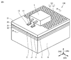
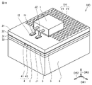
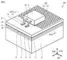
- FIG. 1 is a perspective view schematically showing the configuration of a semiconductor device according to a first embodiment
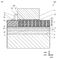
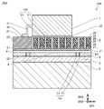
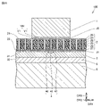
- FIG. FIG. 2 is a cross-sectional view taken along line II-II of FIG. 1
- FIG. 2 is a cross-sectional view taken along line III-III of FIG. 1
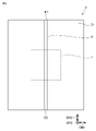
- 2 is a top view schematically showing the configuration of the heat diffusion plate of the semiconductor device according to Embodiment 1
- FIG. 1 is a circuit diagram schematically showing a configuration of a power converter including a semiconductor device according to Embodiment 1
- FIG. 1 is a perspective view schematically showing a configuration of a main circuit of a power converter including a semiconductor device according to Embodiment 1
- FIG. 2 is a top view schematically showing how the semiconductor device according to the first embodiment is put into a reflow furnace;
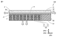
- FIG. FIG. 2 is a cross-sectional view schematically showing a state in which a substrate and a thermal diffusion plate of the semiconductor device according to Embodiment 1 are joined by a joining member;
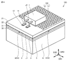
- FIG. 10 is a perspective view schematically showing the configuration of a semiconductor device according to a modification of the first embodiment;
- FIG. 10 is a cross-sectional view schematically showing a configuration of a semiconductor device according to a modification of Embodiment 1;
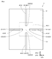
- FIG. 11 is a perspective view schematically showing the configuration of a semiconductor device according to a second embodiment;
- FIG. 11 is a top view schematically showing the structure of a heat diffusion plate of a semiconductor device according to a second embodiment;
- FIG. 11 is a top view schematically showing the structure of a thermal diffusion plate of a semiconductor device according to a first modification of the second embodiment;
- FIG. 11 is a top view schematically showing the configuration of a thermal diffusion plate of a semiconductor device according to a second modification of the second embodiment;
- FIG. 11 is a perspective view schematically showing the configuration of a semiconductor device according to a third embodiment;
- FIG. 11 is a top view schematically showing the configuration of a heat diffusion plate of a semiconductor device according to Embodiment 3;
- FIG. 14 is a top view schematically showing the structure of a thermal diffusion plate of a semiconductor device according to a fourth embodiment;
- FIG. 21 is a top view schematically showing the structure of a thermal diffusion plate of a semiconductor device according to a modification of the fourth embodiment;
- FIG. 21 is a perspective view schematically showing the configuration of a semiconductor device according to a fifth embodiment;
- FIG. 19 is a cross-sectional view along line XIX-XIX in FIG. 18;
- FIG. 14 is a cross-sectional view schematically showing the configuration of a semiconductor device according to a sixth embodiment;
- FIG. 21 is a top view schematically showing the structure of a heat diffusion plate of a semiconductor device according to a sixth embodiment;
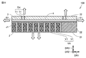
- FIG. 14 is a cross-sectional view schematically showing a state in which a substrate and a thermal diffusion plate of a semiconductor device according to a sixth embodiment are joined by a joining member;
- FIG. 21 is a perspective view schematically showing the configuration of a semiconductor device according to a seventh embodiment
- FIG. 24 is a cross-sectional view along line XXIV-XXIV of FIG. 23
- FIG. 21 is a cross-sectional view of a semiconductor device according to a seventh embodiment, in which the structure of the groove is changed
- FIG. 21 is a cross-sectional view of a semiconductor device according to a seventh embodiment, in which the structure of the groove is changed;
- Embodiment 1 A configuration of a semiconductor device 100 according to the first embodiment will be described with reference to FIGS. 1 to 5.
- FIG. The semiconductor device 100 according to this embodiment may be used in a power conversion device mounted on a hybrid car, an electric vehicle, or the like.
- the semiconductor device 100 includes a semiconductor element 1, a substrate 2, a heat diffusion plate 3, and a bonding member J1.
- Semiconductor device 100 of the present embodiment further includes heat dissipation member 5, cooling body 6, and connection member J2.
- the semiconductor element 1, the connection member J2, the substrate 2, the joint member J1, the thermal diffusion plate 3, the heat dissipation member 5 and the cooling body 6 are laminated in this order.
- the semiconductor element 1 is an electronic component that generates heat.
- Semiconductor device 100 is configured such that heat generated from semiconductor element 1 is dissipated through substrate 2 , heat diffusion plate 3 , heat dissipation member 5 and cooling body 6 .
- the semiconductor element 1 is, for example, a semiconductor chip such as a metal oxide semiconductor field effect transistor (MOSFET) or an insulated gate bipolar transistor (IGBT).
- MOSFET metal oxide semiconductor field effect transistor
- IGBT insulated gate bipolar transistor
- the semiconductor chip may be configured as a package sealed with resin.
- a semiconductor element 1 is bonded to the substrate 2 .
- the thermal diffusion plate 3 is larger than the semiconductor element 1 when viewed from the direction (Z-axis direction DR3) in which the substrate 2 and the thermal diffusion plate 3 sandwich the bonding member J1.
- the semiconductor element 1 overlaps the thermal diffusion plate 3 in the sandwiching direction (Z-axis direction DR3).
- the direction in which the bonding member J1 is sandwiched between the substrate 2 and the heat diffusion plate 3 is the Z-axis direction DR3.
- the direction in which the leads 11 protrude from the semiconductor element 1 is the Y-axis direction DR2.
- a direction intersecting with each of Y-axis direction DR2 and Z-axis direction DR3 is X-axis direction DR1.
- the board 2 is, for example, a printed board.
- Substrate 2 includes a first surface 21 and a second surface 22 .
- the semiconductor element 1 is joined to the first surface 21 of the substrate 2 by a connection member J2.
- the second surface 22 of the substrate 2 is arranged on the side opposite to the semiconductor element 1 with respect to the first surface 21 .
- the second surface 22 of the substrate 2 is joined to the heat diffusion plate 3 by a joining member J1.
- a via hole VH penetrating through the first surface 21 and the second surface 22 is provided in the substrate 2 .
- the via hole VH is provided along the Z-axis direction DR3.
- via hole VH includes a plurality of hole portions V1.
- the connection member J2 overlaps the plurality of hole portions V1 when viewed from the Z-axis direction DR3.
- the plurality of hole portions V1 are arranged at intervals from each other.
- a conductor film such as copper is formed on the inner wall surface of the via hole VH.
- the conductor film may be one in which the holes are filled with a conductive adhesive or solder mixed with silver filler, for example.
- a via hole VH formed by filling a conductive adhesive or the like in this way can have a larger region made of a conductive member having a higher thermal conductivity than a hollow via hole VH, and thus contributes to further improvement in heat dissipation. can do.
- the substrate 2 may include non-penetrating regions 20 .
- No via hole VH is provided in the non-penetrating region 20 .
- the outline of the non-penetrating region 20 is indicated by dashed lines.
- an electrode 12 is arranged in the non-penetrating region 20 .
- Leads 11 of semiconductor element 1 are electrically connected to electrodes 12 in non-penetrating regions 20 .
- the substrate 2 includes a plurality of insulating layers 25, a first conductor layer 26, a second conductor layer 27, and a plurality of third conductor layers 28.
- the plurality of insulating layers 25 have, for example, a flat plate shape.
- the top view shape of the plurality of insulating layers 25 is, for example, a rectangle.
- the material of the insulating layer 25 is, for example, mixed glass fiber and epoxy resin. Also, the material of the insulating layer 25 is not limited to this, and may be a mixture of aramid resin and epoxy resin.
- the first conductor layer 26 and the second conductor layer 27 sandwich a plurality of insulating layers 25 .
- the first surface 21 of the substrate 2 is provided on the first conductor layer 26 .
- the second surface 22 of the substrate 2 is provided on the second conductor layer 27 .
- Each of the plurality of third conductor layers 28 is arranged between each of the plurality of insulating layers 25 . Therefore, each of the plurality of third conductor layers 28 is spaced apart from the first conductor layer 26 and the second conductor layer 27 .
- Each of the plurality of insulating layers 25, the first conductor layers 26, the second conductor layers 27 and the plurality of third conductor layers 28 may be arranged parallel to each other.
- the materials of the first conductor layer 26, the second conductor layer 27 and the plurality of third conductor layers 28 are, for example, metals with high thermal conductivity such as copper (Cu).
- the thicknesses of the first conductor layer 26, the second conductor layer 27 and the plurality of third conductor layers 28 are, for example, 100 ⁇ m.
- the substrate 2 includes two third conductor layers 28, but the number of third conductor layers 28 is not limited to this.
- the heat diffusion plate 3 is bonded to the second surface 22 of the substrate 2 with a bonding member J1.
- the thermal diffusion plate 3 and the substrate 2 sandwich the joining member J1.
- the heat diffusion plate 3 includes a surface 31 to be joined and an opposing surface 32 .
- the bonding surface 31 is arranged on the opposite side of the substrate 2 from the semiconductor element 1 .
- the bonded surface 31 is bonded to the substrate 2 by a bonding member J1.
- the facing surface 32 is arranged on the opposite side of the bonding member J1 from the surface 31 to be bonded.
- the facing surface 32 faces the surface 31 to be joined.
- the heat radiating member 5 is joined to the facing surface 32 .
- the heat diffusion plate 3 is provided with grooves 4 that are recessed from the joint surface 31 .
- the direction (depth direction) in which the groove 4 is recessed from the surface to be bonded 31 is along the direction (Z-axis direction DR3) in which the bonding member J1 is superimposed on the surface to be bonded 31 .
- the width of the groove 4 is uniform along the direction (Z-axis direction DR3) from the surface to be joined 31 toward the opposing surface 32.
- the depth of the groove 4 may be determined appropriately as long as it does not penetrate the heat diffusion plate 3 .
- the grooves 4 of the heat diffusion plate 3 include portions exposed from the joining member J1. Therefore, the grooves 4 of the heat diffusion plate 3 communicate with the outside of the semiconductor device 100 .
- the length of the printed circuit board and the heat diffusion plate 3 are the same. The substrate-side surface of the plate 3 is not exposed to the outside.
- the groove 4 includes a first end E1 and a second end E2.
- the first end E1 and the second end E2 are both ends of the groove 4 in the longitudinal direction.
- the first end E ⁇ b>1 and the second end E ⁇ b>2 of the groove 4 are provided at the ends of the heat diffusion plate 3 .
- Each of the first end E1 and the second end E2 is exposed from the joining member J1. Therefore, the grooves 4 of the heat diffusion plate 3 are exposed from the joint member J1 on the sides of the heat diffusion plate 3 .
- the material of the heat diffusion plate 3 is, for example, copper (Cu). Therefore, the heat diffusion plate 3 is, for example, a copper plate.
- the heat diffusion plate 3 is not limited to this, and may be aluminum oxide (Al 2 O 3 ) having a metal film such as copper (Cu) formed on the surface, for example.
- the heat diffusion plate 3 is a metal plate of copper (Cu) alloy, aluminum (Al) alloy or magnesium (Mg) alloy plated with nickel (Ni), gold (Au) or tin (Sn). It may be formed of a metal material.
- the thickness of the heat diffusion plate 3 is, for example, 0.1 mm. When the thickness of the heat diffusion plate 3 is 0.1 mm or more, both the thermal conductivity (heat dissipation) and strength of the heat diffusion plate 3 are improved. Note that the thickness of the heat diffusion plate 3 may be less than 0.1 mm.
- the joining member J1 joins the substrate 2 and the thermal diffusion plate 3 between the substrate 2 and the thermal diffusion plate 3 .
- the connection member J2 joins the semiconductor element 1 and the substrate 2 between the semiconductor element 1 and the substrate 2 .
- the joining member J1 and the connecting member J2 are, for example, solder.
- the joining member J1 and the connecting member J2 may be conductive adhesives such as silver (Ag) paste and nickel (Ni) paste, for example.
- the joining member J1 and the connecting member J2 are configured to melt when heated.
- the joining member J1 is configured to join the substrate 2 and the heat diffusion plate 3 together.
- the connection member J2 is configured to join the semiconductor element 1 and the substrate 2 together.
- the flux evaporates when the joint member J1 melts.
- the flux evaporates when the connection member J2 melts.
- the heat dissipation member 5 sandwiches the heat diffusion plate 3 with the substrate 2 .
- the heat dissipation member 5 is, for example, a metal plate such as copper (Cu).
- the heat radiating member 5 is sandwiched between the cooling body 6 and the heat diffusion plate 3 .
- the cooling body 6 may be, for example, the housing of the semiconductor device 100 .
- the cooling body 6 may be a heat pipe, a radiation fin, or the like.
- the outer shape of the semiconductor element 1 is indicated by broken lines.
- the width of the semiconductor element 1 is larger than the width of the groove 4 when viewed from the Z-axis direction DR3.
- the semiconductor element 1 overlaps the groove 4 in the Z-axis direction DR3. It is desirable that the area of the groove 4 in top view is 50% or less of the area of the lamination region 10 .
- the power converter 200 includes an inverter circuit 210 , a transformer circuit 220 , a rectifier circuit 230 , a smoothing circuit 240 and a control circuit 250 .
- a semiconductor device 100 (see FIG. 1) according to the present embodiment is applied to an inverter circuit 210 and a rectifier circuit 230, for example. Therefore, the power conversion device 200 includes the semiconductor device 100 (see FIG. 1).
- Semiconductor device 100 is a part of power conversion device 200 .
- FIG. 5A is a perspective view schematically showing the configuration of the power conversion device 200.
- FIG. The portion I surrounded by the dashed line in FIG. 5A is the portion of FIG.
- the inverter circuit 210 includes a first switching element 211, which is the semiconductor element 1, a second switching element 212, a third switching element 213, and a fourth switching element 214.
- the series-connected first switching element 211 and three switching elements are connected in parallel with the series-connected second switching element 212 and fourth switching element 214 .
- Each of the first switching element 211, the second switching element 212, the third switching element 213, and the fourth switching element 214 is, for example, a metal oxide semiconductor field effect transistor (MOSFET), an insulated gate type A bipolar transistor (IGBT: Insulated Gate Bipolar Transistor) or the like.
- MOSFET metal oxide semiconductor field effect transistor
- IGBT Insulated Gate Bipolar Transistor
- Each material of the first switching element 211, the second switching element 212, the third switching element 213, and the fourth switching element 214 is silicon (Si), silicon carbide (SiC), or gallium nitride (GaN), for example.
- the transformer circuit 220 includes a first coil device 221.
- the first coil device 221 is configured as a transformer.
- the first coil device 221 includes a first coil 2221 and a second coil 2222 .
- the first coil 2221 is a primary side coil conductor connected to the inverter circuit 210 . That is, the first coil 2221 is the high voltage side winding.
- a second coil 2222 is a secondary coil conductor connected to the rectifier circuit 230 . That is, the second coil 2222 is the low voltage side winding.
- the rectifier circuit 230 includes a first diode 231 , a second diode 232 , a third diode 233 and a fourth diode 234 .
- a first diode 231 and a third diode 233 connected in series are connected in parallel with a second diode 232 and a fourth diode 234 connected in series.
- Each material of the first diode 231, the second diode 232, the third diode 233, and the fourth diode 234 is silicon (Si), silicon carbide (SiC), or gallium nitride (GaN), for example.
- the smoothing circuit 240 includes a second coil device 241 and a first capacitor 242.
- the second coil device 241 is configured as a smoothing coil.
- the control circuit 250 is configured to output a control signal for controlling the inverter circuit 210 to the inverter circuit 210 .
- the inverter circuit 210 is configured to convert an input voltage and output the converted voltage.
- the power conversion device 200 further includes a third coil device 260, a fourth coil device 270, and a second capacitor 280.
- the third coil device 260 and the second capacitor 280 are arranged before the inverter circuit 210 .
- the third coil device 260 is configured as a smoothing coil.
- the fourth coil device 270 is arranged between the inverter circuit 210 and the transformer circuit 220 . More specifically, the fourth coil device 270 is arranged between the first switching element 211 and the third switching element 213 and the first coil.
- the power conversion device 200 is configured to receive a DC voltage of 100 V or more and 600 V or less.
- the power converter 200 is configured to output a DC voltage of 12 V or more and 600 V or less, for example.
- the DC voltage input to the input terminal 291 of the power converter 200 is converted into the first AC voltage by the inverter circuit 210 .
- the transformer circuit 220 is configured to transform the first AC voltage into a second AC voltage having a lower voltage value than the first AC voltage.
- Rectifier circuit 230 is configured to rectify the second AC voltage.
- Smoothing circuit 240 is configured to smooth the voltage output from rectifying circuit 230 .
- the power converter 200 is configured to output the DC voltage output from the smoothing circuit 240 from the output terminal 292 .
- the voltage value of the input DC voltage Vi may be greater than the voltage value of the output DC voltage Vo.
- FIG. 1 a method for manufacturing the semiconductor device 100 according to the first embodiment will be described with reference to FIGS. 3, 6 and 7.
- FIG. 1
- the manufacturing method of the semiconductor device 100 includes a preparation process and a bonding process.
- a preparation step as shown in FIG. 3, a semiconductor element 1, a substrate 2, a thermal diffusion plate 3, and a bonding member J1 are prepared.
- the heat radiating member 5, the cooling body 6, and the connecting member J2 are further prepared in the preparation steps.
- the bonding member J1 sandwiched between the substrate 2 and the bonding surface 31 of the thermal diffusion plate 3 is heated to melt the bonding member J1.
- the substrate 2 and the bonded surface 31 of the heat diffusion plate 3 are bonded by J1.
- the bonding member J ⁇ b>1 sandwiched between the substrate 2 and the bonded surface 31 of the heat diffusion plate 3 is spaced apart from the bottom of the groove 4 of the heat diffusion plate 3 .
- the semiconductor element 1 (see FIG. 3) is bonded to the substrate 2 on the opposite side of the substrate 2 from the heat diffusion plate 3 .
- the connection member J2 (see FIG. 3) sandwiched between the semiconductor element 1 (see FIG. 3) and the substrate 2 the melted connection member J2 (see FIG. 3) is applied to the substrate. 2 and the semiconductor element 1 (see FIG. 3) are bonded.
- a paste-like joining member J1 is applied onto the wiring pattern (not shown) on the second surface 22 of the substrate 2 .
- the second surface 22 of the substrate 2 is arranged on the upper side along the direction of gravity.
- the thermal diffusion plate 3 is arranged so as to sandwich the applied paste-like joining member J1 with the substrate 2 .
- the substrate 2, the heat diffusion plate 3 and the joining member J1 are put into the reflow furnace RF (see FIG. 6) and heated.
- the substrate 2 and the thermal diffusion plate 3 are bonded together by the melted bonding member J1. Flux evaporates from the melted joint member J1.
- the flux evaporated from the melted joint member J1 is discharged to the outside of the semiconductor device 100 through the grooves 4 of the thermal diffusion plate 3 and the via holes VH.
- the direction in which the flux is discharged from the semiconductor device 100 is indicated by an outline arrow.
- the substrate 2 to which the heat diffusion plate 3 is bonded is then turned over. Thereby, the first surface 21 of the substrate 2 is arranged upward along the direction of gravity.
- a paste-like connection member J ⁇ b>2 is applied to the first surface 21 of the substrate 2 .
- the semiconductor element 1 is arranged on the applied paste-like connecting member J2.
- the semiconductor element 1, the substrate 2, the thermal diffusion plate 3, the joining member J1 and the connecting member J2 are heated by the reflow furnace RF (see FIG. 6).
- the semiconductor element 1 and the semiconductor element 1 are joined by the melted connection member J2. Flux evaporates from the melted connection member J2.
- the heat dissipation member 5 is joined to the heat diffusion plate 3 .
- the cooling body 6 is joined to the heat radiating member 5 .
- the bonding member J1 may enter a part of the interior of the groove 4, or the bonding member J1 may not enter the interior of the groove 4. good.
- FIG. 8 the configuration of the semiconductor device 100 according to the modification of the first embodiment will be described with reference to FIGS. 8 and 9.
- the first end E1 and the second end E2 of the groove 4 of the thermal diffusion plate 3 of the semiconductor device 100 according to the modification of the first embodiment correspond to the ends of the thermal diffusion plate 3. is placed inside.
- the first end E ⁇ b>1 and the second end E ⁇ b>2 of the groove 4 are not arranged at the end of the heat diffusion plate 3 .
- the joining member J1 is arranged inside the first end E1 and the second end E2 of the groove 4 . Therefore, the joint member J1 does not reach the end of the heat diffusion plate 3 .
- the semiconductor device according to the comparative example has the same configuration as the semiconductor device 100 according to the present embodiment unless otherwise specified.
- the groove 4 is not provided in the bonding surface 31 . Therefore, the heat diffusion plate 3 is in close contact with the joint member J1 when the joint member J1 is melted. Therefore, the flux evaporated from the melted joint member J1 remains inside the joint member J1. As a result, voids are generated inside the joint member J1 after the joint member J1 is melted. If voids remain inside the bonding member J1, the voids increase the thermal resistance of the bonding member J1. Therefore, the heat dissipation of the semiconductor element 1 is deteriorated due to the voids.
- the grooves 4 of the thermal diffusion plate 3 include portions exposed from the bonding member J1. Therefore, the flux evaporated from the bonding member J1 melted when the substrate 2 and the thermal diffusion plate 3 are bonded is discharged to the outside of the semiconductor device 100 through the grooves 4 of the thermal diffusion plate 3 . Therefore, it is possible to suppress the generation of voids inside the bonding member J1. Therefore, voids in the joint member J1 can be reduced.
- the voids in the joint member J1 can be reduced, it is possible to suppress an increase in the thermal resistance of the joint member J1 due to the voids. Therefore, it is possible to suppress deterioration of the heat dissipation property of the semiconductor element 1 due to voids.
- the heat generated from the semiconductor element 1 is mainly conducted along the Z-axis direction DR3 through the connecting member J2, the substrate 2, the joining member J1, and the thermal diffusion plate 3 in this order. Therefore, the heat generated from the semiconductor element 1 is conducted along the thickness direction (Z-axis direction DR3) of the bonding member J1. Since the voids in the bonding member J1 can be reduced, it is possible to suppress the decrease in the thermal resistance along the thickness direction of the bonding member J1 due to the voids. Therefore, heat generated from the semiconductor element 1 is easily conducted along the thickness direction (Z-axis direction DR3) of the bonding member J1. Therefore, the heat generated from semiconductor element 1 is easily dissipated.
- the thermal diffusion plate 3 is larger than the semiconductor element 1 when viewed from the direction (Z-axis direction DR3) in which the substrate 2 and the thermal diffusion plate 3 sandwich the bonding member J1.
- the semiconductor element 1 overlaps the thermal diffusion plate 3 in the sandwiching direction (Z-axis direction DR3). Therefore, the heat generated from the semiconductor element 1 is dissipated through the thermal diffusion plate 3 overlaid on the semiconductor element 1 . Therefore, the heat dissipation of the semiconductor element 1 is further improved.
- each of the first end E1 and the second end E2 of the groove 4 is exposed from the joining member J1. Therefore, the flux passes through the groove 4 to the semiconductor device 100 more than when one of the first end E1 and the second end E2 of the groove 4 is exposed from the bonding member J1 and the other is not exposed from the bonding member J1. Almost discharged to the outside. Therefore, voids in the joint member J1 can be further reduced.
- the first end E1 of the groove 4 is provided at the end of the heat diffusion plate 3. Therefore, the first end E ⁇ b>1 of the groove 4 is exposed to the outside of the semiconductor device 100 from the end of the heat diffusion plate 3 . Therefore, the flux evaporated from the melted bonding member J1 is discharged to the outside of the semiconductor device 100 through the first end E1 more than when the first end E1 of the groove 4 is not exposed at the end of the semiconductor device 100. Cheap. Therefore, voids in the joint member J1 can be further reduced.
- Embodiment 2 the configuration of the semiconductor device 100 according to the second embodiment will be described with reference to FIGS. 10 to 13.
- FIG. The second embodiment has the same configuration, manufacturing method, and effects as those of the first embodiment unless otherwise specified. Therefore, the same reference numerals are given to the same configurations as in the above-described first embodiment, and description thereof will not be repeated.
- the groove 4 of the thermal diffusion plate 3 of the semiconductor device 100 includes a first groove portion 41 and a second groove portion .
- Each of the first groove portion 41 and the second groove portion 42 includes a portion exposed from the joint member J1.
- each of the first end E11 (E1) and the second end E12 (E2) of the first groove portion 41 is exposed from the joining member J1.
- each of the first end E21 (E1) and the second end E22 (E2) of the second groove portion 42 is exposed from the joint member J1.
- first groove portion 41 and the second groove portion 42 are spaced apart from each other. In other words, the first groove portion 41 and the second groove portion 42 do not cross each other.
- the first groove portion 41 and the second groove portion 42 may be arranged parallel to each other.
- Each of first groove portion 41 and second groove portion 42 may extend along X-axis direction DR1.
- the first groove portion 41 and the second groove portion 42 may extend along the Y-axis direction DR2.
- the first groove portion 41 and the second groove portion 42 may extend obliquely with respect to each of the X-axis direction DR1 and the Y-axis direction DR2.
- the number of grooves is not limited to two.
- each of the first end E11 (E1) and the second end E12 (E2) of the first groove portion 41 and the first end E21 (E1) and the second end E22 (E2) of the second groove portion 42 extend from the joint member J1.
- the portion exposed from the joint member J1 is not limited to this.
- the first end E11 (E1) of the first groove portion 41 and the first end E21 (E1) of the second groove portion 42 are exposed and the second end E12 (E2) of the first groove portion 41 and the second end E12 (E2) of the second groove portion 42 are exposed.
- the two ends E22 (E2) may not be exposed.
- first groove portion 41 and second groove portion 42 each include a portion exposed from bonding member J1. Therefore, the area where the joint member J1 and the groove 4 face each other can be made larger than when the groove 4 is formed of one groove portion (see FIG. 1). Therefore, the flux evaporated from the melted joint member J1 is discharged to the outside of the semiconductor device 100 through the groove 4 . Therefore, voids in the joint member J1 can be further reduced.
- the first groove portion 41 and the second groove portion 42 are spaced apart from each other. Therefore, the heat diffusion plate 3 has a simpler shape than when the first grooves 41 and the second grooves 42 cross each other. Therefore, since the heat diffusion plate 3 can be easily manufactured, the manufacturing cost of the semiconductor device 100 can be reduced.
- Embodiment 3 Next, the configuration of the semiconductor device 100 according to the third embodiment will be described with reference to FIGS. 14 and 15.
- FIG. Embodiment 3 has the same configuration, manufacturing method, and effects as those of Embodiment 2 described above unless otherwise specified. Therefore, the same reference numerals are given to the same configurations as in the second embodiment, and the description thereof will not be repeated.
- first groove portion 41 and the second groove portion 42 of the thermal diffusion plate 3 of the semiconductor device 100 intersect each other.
- the first groove portion 41 and the second groove portion 42 are arranged, for example, in a cross shape.
- first groove portion 41 extends along X-axis direction DR1.
- the second groove portion 42 extends along the Y-axis direction DR2.
- the intersection of the first groove 41 and the second groove 42 overlaps the semiconductor element 1 when viewed from the direction (Z-axis direction DR3) in which the semiconductor element 1 is stacked on the heat diffusion plate 3 .
- the intersection of the first groove 41 and the second groove 42 overlaps the center of the semiconductor element 1 when viewed from the direction (Z-axis direction DR3) in which the semiconductor element 1 is stacked on the heat diffusion plate 3. .
- first groove 41 and second groove 42 cross each other. Therefore, the portions of the first groove portion 41 and the second groove portion 42 exposed from the joint member J1 are exposed from the joint member J1 (see FIG. 14) along mutually different directions. Therefore, the flux evaporated from the bonding member J1 (see FIG. 14) can be discharged to the outside of the semiconductor device 100 along the direction in which the first groove portion 41 and the second groove portion 42 are exposed to each other. That is, flux evaporated from the bonding member J1 (see FIG.
- Embodiment 4 the configuration of the semiconductor device 100 according to the fourth embodiment will be described with reference to FIGS. 16 and 17.
- FIG. The fourth embodiment has the same configuration, manufacturing method, and effects as those of the third embodiment unless otherwise specified. Therefore, the same reference numerals are assigned to the same configurations as those of the above-described third embodiment, and description thereof will not be repeated.
- the bonded surface 31 of the thermal diffusion plate 3 of the semiconductor device 100 includes the laminated region 10.
- the semiconductor element 1 is stacked on the stacked region 10 .
- the semiconductor element 1 is stacked on the stacked region 10 along the Z-axis direction DR3.
- a first end E1 of the groove 4 is exposed from the joint member J1 (see FIG. 1).
- a second end E2 of the groove 4 is arranged between the center C1 of the lamination region 10 of the surface 31 to be joined and the first end E1.
- the groove 4 is not provided in the center C1 of the lamination region 10 of the surface 31 to be joined.
- a center C1 of the lamination region 10 of the bonding surface 31 is bonded to the substrate 2 (see FIG. 1) by a bonding member J1 (see FIG. 1).
- the groove 4 includes a first groove portion 41, a second groove portion 42, a third groove portion 43 and a fourth groove portion 44.
- the first groove portion 41 and the second groove portion 42 are provided so as to be orthogonal to each other.
- the 3rd groove part 43 and the 4th groove part 44 are provided so that it may mutually orthogonally cross.
- the first groove portion 41 and the third groove portion 43 are arranged with a gap therebetween along the X-axis direction DR1.
- the second groove portion 42 and the fourth groove portion 44 are arranged with a gap therebetween along the Y-axis direction DR2.
- the first ends E11(E1) to E41(E1) of the first groove portion 41 to the fourth groove portion 44 are exposed from the joint member J1 (see FIG. 1).
- Each of the second ends E12 (E2) to E42 (E2) of the first groove portion 41 to the fourth groove portion 44 is aligned with the center C1 of the laminated region 10 of the surface to be joined 31 and the first ends E11 (E1) to E41 (E1). are placed between each.
- the groove 4 includes a first groove portion 41 to an eighth groove portion 48.
- the first to eighth grooves 41 to 48 are arranged radially.
- the first ends E11(E1) to E81(E1) of the first groove portion 41 to the eighth groove portion 48 are exposed from the joint member J1 (see FIG. 1).
- Each of the second ends E12 (E2) to E82 (E2) of the first groove portion 41 to the eighth groove portion 48 is aligned with the center C1 of the laminated region 10 of the surface to be joined 31 and the first ends E11 (E1) to E81 (E1). are placed between each.
- the center C1 of the lamination region 10 of the bonding surface 31 is separated from the substrate 2 (see FIG. 1) by the bonding member J1 (see FIG. 1). is joined to Therefore, the groove 4 is not provided in the center C1 of the laminated region 10 of the surface 31 to be bonded. Since an air layer is formed inside the groove 4, if the groove 4 were provided at the center C1 of the lamination region 10 of the bonding surface 31, the heat dissipation of the semiconductor element 1 would be deteriorated by the air layer.
- the groove 4 is not provided in the center C1 of the lamination region 10 of the bonding surface 31 , it is possible to suppress the deterioration of the heat dissipation of the semiconductor element 1 due to the air layer of the groove 4 . In other words, it is possible to suppress an increase in the thermal resistance of the heat diffusion plate 3 due to the air layer in the grooves 4 .
- Embodiment 5 the configuration of the semiconductor device 100 according to the fifth embodiment will be described with reference to FIGS. 18 and 19.
- FIG. The fifth embodiment has the same configuration, manufacturing method, and effects as those of the first embodiment unless otherwise specified. Therefore, the same reference numerals are given to the same configurations as in the above-described first embodiment, and description thereof will not be repeated.
- the groove 4 of the heat diffusion plate 3 of the semiconductor device 100 has a width that is configured to decrease from the facing surface 32 toward the bonded surface 31 .
- groove 4 includes bottom 45 , first side 46 and second side 47 .
- the bottom portion 45 faces the joint member J1.
- Each of the first side surface 46 and the second side surface 47 connects the surface to be joined 31 and the bottom portion 45 .
- the distance between the first side surface 46 and the second side surface 47 is configured to decrease from the opposing surface 32 toward the surface 31 to be joined.
- the groove 4 has a width that is configured to decrease from the facing surface 32 toward the bonded surface 31 . Therefore, when the substrate 2 and the heat diffusion plate 3 are bonded together by the reflow furnace RF (see FIG. 6), it is possible to prevent the melted bonding member J1 from entering the groove 4 . In other words, it is possible to prevent the groove 4 from being clogged by the melted joint member J1. If the groove 4 is blocked by the melted bonding member J1, flux is prevented from being discharged to the outside of the semiconductor device 100 through the groove 4 . In the present embodiment, since it is possible to prevent the groove 4 from being blocked by the bonding member J1, it is possible to prevent the flux from being prevented from being discharged to the outside of the semiconductor device 100 through the groove 4. .
- Embodiment 6 the configuration of the semiconductor device 100 according to the sixth embodiment will be described with reference to FIGS. 20 to 22.
- FIG. The sixth embodiment has the same configuration, manufacturing method, and effects as those of the first embodiment, unless otherwise specified. Therefore, the same reference numerals are given to the same configurations as in the above-described first embodiment, and description thereof will not be repeated.
- the thermal diffusion plate 3 of the semiconductor device 100 is provided with through holes TH.
- the through hole TH penetrates the heat diffusion plate 3 along the direction (Z-axis direction DR3) in which the bonding member J1 is superimposed on the surface 31 to be bonded.
- the diffusion plate 3 is provided with a through hole TH so as to overlap the bonding member J1 along the overlapping direction (DR3).
- the through hole TH is provided in at least one of the surface to be joined 31 and the recess.
- the diameter of the through hole TH is smaller than the diameter of the via hole VH.
- the diameter of the through-hole TH may be appropriately determined as long as the diameter does not allow the joining member J1 melted by the reflow furnace RF (see FIG. 6) to enter.
- the through-hole TH may include a plurality of first through-holes T1 and a plurality of second through-holes T2.
- Each of the plurality of first penetrating portions T1 and the plurality of second penetrating portions T2 penetrates the thermal diffusion plate 3 along the direction (Z-axis direction DR3) in which the bonding member J1 is superimposed on the surface 31 to be bonded.
- the multiple first penetrating portions T1 communicate with the grooves 4 .
- the plurality of second penetrating portions T2 communicate with the surface 31 to be joined.
- the through hole TH allows thermal diffusion along the direction (Z-axis direction DR3) in which the bonding member J1 is superimposed on the surface 31 to be bonded. It penetrates the plate 3. Therefore, when the substrate 2 and the thermal diffusion plate 3 are bonded by the reflow furnace RF (see FIG. 6), the flux evaporated from the molten bonding member J1 is added to the grooves 4 as shown in FIG. , and is discharged to the outside of the semiconductor device 100 through the through hole TH. As a result, when the substrate 2 and the thermal diffusion plate 3 are bonded together by the reflow furnace RF (see FIG. 6), the flux evaporated from the melted bonding member J1 is discharged to the outside of the semiconductor device 100 . Therefore, voids in the joint member J1 can be further reduced.
- Embodiment 7 the configuration of the semiconductor device 100 according to the seventh embodiment will be described with reference to FIGS. 23 and 24.
- FIG. The seventh embodiment has the same configuration, manufacturing method, and effects as those of the first embodiment unless otherwise specified. Therefore, the same reference numerals are given to the same configurations as in the above-described first embodiment, and description thereof will not be repeated.
- the groove 4 of the heat diffusion plate 3 of the semiconductor device 100 has a width that increases from the facing surface 32 toward the surface 31 to be bonded. have.
- groove 4 includes bottom 45 , first side 46 and second side 47 .
- the bottom portion 45 faces the joint member J1.
- Each of the first side surface 46 and the second side surface 47 connects the surface to be joined 31 and the bottom portion 45 .
- the distance between the first side surface 46 and the second side surface 47 is configured to decrease from the surface 31 to be joined toward the opposing surface 32 .
- the processing method of the groove 4 is not particularly limited, and any of the shapes of Embodiments 1 to 7 can be manufactured by processing methods such as press punching, etching, wire electric discharge machining (wire cutting), and laser machining.
- the grooves 4 of the thermal diffusion plate 3 of the semiconductor device 100 according to the present embodiment extend from the facing surface 32 to the bonding surface. It has a width that is configured to increase towards 31 . Therefore, when the substrate 2 and the heat diffusion plate 3 are bonded together by the reflow furnace RF (see FIG. 6), the melted bonding member J1 can easily enter the groove 4 . In other words, the groove 4 is closed by the melted joint member J1, and the entire groove 4 is filled with the joint member J1.
- the groove 4 that was an air layer is filled with the bonding member J1. Thermal resistance can be reduced. Therefore, heat dissipation of the semiconductor device 100 can be improved.
Landscapes
- Cooling Or The Like Of Semiconductors Or Solid State Devices (AREA)
Priority Applications (1)
| Application Number | Priority Date | Filing Date | Title |
|---|---|---|---|
| JP2023506981A JP7550958B2 (ja) | 2021-03-15 | 2022-03-07 | 半導体装置および電力変換装置 |
Applications Claiming Priority (2)
| Application Number | Priority Date | Filing Date | Title |
|---|---|---|---|
| JP2021041268 | 2021-03-15 | ||
| JP2021-041268 | 2021-03-15 |
Publications (1)
| Publication Number | Publication Date |
|---|---|
| WO2022196411A1 true WO2022196411A1 (ja) | 2022-09-22 |
Family
ID=83320424
Family Applications (1)
| Application Number | Title | Priority Date | Filing Date |
|---|---|---|---|
| PCT/JP2022/009704 Ceased WO2022196411A1 (ja) | 2021-03-15 | 2022-03-07 | 半導体装置および電力変換装置 |
Country Status (2)
| Country | Link |
|---|---|
| JP (1) | JP7550958B2 (https=) |
| WO (1) | WO2022196411A1 (https=) |
Citations (4)
| Publication number | Priority date | Publication date | Assignee | Title |
|---|---|---|---|---|
| JPH0718451U (ja) * | 1993-08-27 | 1995-03-31 | 株式会社明電舎 | 半導体装置 |
| JP2004356261A (ja) * | 2003-05-28 | 2004-12-16 | Mitsubishi Electric Corp | 電力用半導体装置 |
| JP2014160707A (ja) * | 2013-02-19 | 2014-09-04 | Mitsubishi Materials Corp | 接合体の製造方法、パワーモジュールの製造方法、及びパワーモジュール |
| WO2017188246A1 (ja) * | 2016-04-26 | 2017-11-02 | 三菱電機株式会社 | 電力用回路装置 |
-
2022
- 2022-03-07 WO PCT/JP2022/009704 patent/WO2022196411A1/ja not_active Ceased
- 2022-03-07 JP JP2023506981A patent/JP7550958B2/ja active Active
Patent Citations (4)
| Publication number | Priority date | Publication date | Assignee | Title |
|---|---|---|---|---|
| JPH0718451U (ja) * | 1993-08-27 | 1995-03-31 | 株式会社明電舎 | 半導体装置 |
| JP2004356261A (ja) * | 2003-05-28 | 2004-12-16 | Mitsubishi Electric Corp | 電力用半導体装置 |
| JP2014160707A (ja) * | 2013-02-19 | 2014-09-04 | Mitsubishi Materials Corp | 接合体の製造方法、パワーモジュールの製造方法、及びパワーモジュール |
| WO2017188246A1 (ja) * | 2016-04-26 | 2017-11-02 | 三菱電機株式会社 | 電力用回路装置 |
Also Published As
| Publication number | Publication date |
|---|---|
| JP7550958B2 (ja) | 2024-09-13 |
| JPWO2022196411A1 (https=) | 2022-09-22 |
Similar Documents
| Publication | Publication Date | Title |
|---|---|---|
| JP2023040253A (ja) | パワー半導体装置およびその製造方法 | |
| US12040301B2 (en) | Semiconductor device | |
| CN107534033B (zh) | 接合体、自带散热器的功率模块用基板、散热器及接合体的制造方法、自带散热器的功率模块用基板的制造方法、散热器的制造方法 | |
| KR101486137B1 (ko) | 방열 장치 및 그 제조 방법 | |
| WO2023221970A1 (zh) | 功率模块、电源系统、车辆及光伏系统 | |
| WO2018194153A1 (ja) | 電力用半導体モジュール、電子部品および電力用半導体モジュールの製造方法 | |
| JP2006134990A (ja) | 半導体装置 | |
| JP2013013933A (ja) | 積層化高融点半田層およびその形成方法、および半導体装置 | |
| JP6244272B2 (ja) | 半導体装置 | |
| JP2021520652A (ja) | 電子モジュールとその製造方法 | |
| WO2011040313A1 (ja) | 半導体モジュールおよびその製造方法 | |
| JP2016181607A (ja) | 半導体装置及びその製造方法 | |
| WO2021208006A1 (zh) | 封装结构、电动车辆和电子装置 | |
| JP2007059860A (ja) | 半導体パッケージ及び半導体モジュール | |
| JP2019212808A (ja) | 半導体装置の製造方法 | |
| WO2014021077A1 (ja) | 多層基板および多層基板を用いたパワーモジュール | |
| JP7550958B2 (ja) | 半導体装置および電力変換装置 | |
| US20230075200A1 (en) | Power module and method for manufacturing same | |
| JP2017063126A (ja) | 抵抗器の製造方法、抵抗器 | |
| JP2011023748A (ja) | 電子機器装置 | |
| CN100418216C (zh) | 半导体封装及半导体模块 | |
| US20260082967A1 (en) | Joint structure, semiconductor device, manufacturing method of joint structure, and manufacturing method of semiconductor device | |
| EP2722885B1 (en) | Surface mountable power components | |
| JP2017188528A (ja) | 半導体装置 | |
| JP7827973B2 (ja) | 半導体装置 |
Legal Events
| Date | Code | Title | Description |
|---|---|---|---|
| 121 | Ep: the epo has been informed by wipo that ep was designated in this application |
Ref document number: 22771165 Country of ref document: EP Kind code of ref document: A1 |
|
| ENP | Entry into the national phase |
Ref document number: 2023506981 Country of ref document: JP Kind code of ref document: A |
|
| NENP | Non-entry into the national phase |
Ref country code: DE |
|
| 122 | Ep: pct application non-entry in european phase |
Ref document number: 22771165 Country of ref document: EP Kind code of ref document: A1 |