WO2022195648A1 - Carte sonde - Google Patents
Carte sonde Download PDFInfo
- Publication number
- WO2022195648A1 WO2022195648A1 PCT/JP2021/010294 JP2021010294W WO2022195648A1 WO 2022195648 A1 WO2022195648 A1 WO 2022195648A1 JP 2021010294 W JP2021010294 W JP 2021010294W WO 2022195648 A1 WO2022195648 A1 WO 2022195648A1
- Authority
- WO
- WIPO (PCT)
- Prior art keywords
- heat
- probe card
- substrate
- wiring board
- coating
- Prior art date
Links
- 239000000523 sample Substances 0.000 title claims abstract description 83
- 238000000576 coating method Methods 0.000 claims abstract description 118
- 239000011248 coating agent Substances 0.000 claims abstract description 111
- 239000000758 substrate Substances 0.000 claims abstract description 81
- OKTJSMMVPCPJKN-UHFFFAOYSA-N Carbon Chemical compound [C] OKTJSMMVPCPJKN-UHFFFAOYSA-N 0.000 claims abstract description 13
- 239000000463 material Substances 0.000 claims abstract description 9
- 229910052799 carbon Inorganic materials 0.000 claims abstract description 7
- 239000002245 particle Substances 0.000 claims abstract description 7
- 239000011230 binding agent Substances 0.000 claims abstract description 6
- 230000002093 peripheral effect Effects 0.000 claims description 21
- 238000010438 heat treatment Methods 0.000 description 20
- 239000004065 semiconductor Substances 0.000 description 19
- 238000007689 inspection Methods 0.000 description 13
- 238000010586 diagram Methods 0.000 description 9
- 238000000034 method Methods 0.000 description 7
- 230000003014 reinforcing effect Effects 0.000 description 4
- 239000002904 solvent Substances 0.000 description 4
- 238000012360 testing method Methods 0.000 description 4
- 239000002041 carbon nanotube Substances 0.000 description 3
- 229910021393 carbon nanotube Inorganic materials 0.000 description 3
- 229910002804 graphite Inorganic materials 0.000 description 3
- 239000010439 graphite Substances 0.000 description 3
- 239000000203 mixture Substances 0.000 description 3
- XLYOFNOQVPJJNP-UHFFFAOYSA-N water Substances O XLYOFNOQVPJJNP-UHFFFAOYSA-N 0.000 description 3
- YCKRFDGAMUMZLT-UHFFFAOYSA-N Fluorine atom Chemical compound [F] YCKRFDGAMUMZLT-UHFFFAOYSA-N 0.000 description 2
- 239000002612 dispersion medium Substances 0.000 description 2
- 229920001971 elastomer Polymers 0.000 description 2
- 239000011737 fluorine Substances 0.000 description 2
- 229910052731 fluorine Inorganic materials 0.000 description 2
- 238000004519 manufacturing process Methods 0.000 description 2
- 239000002184 metal Substances 0.000 description 2
- 229910052751 metal Inorganic materials 0.000 description 2
- 229920002120 photoresistant polymer Polymers 0.000 description 2
- 229920005989 resin Polymers 0.000 description 2
- 239000011347 resin Substances 0.000 description 2
- 239000005060 rubber Substances 0.000 description 2
- 229910000531 Co alloy Inorganic materials 0.000 description 1
- 239000004593 Epoxy Substances 0.000 description 1
- 229910003266 NiCo Inorganic materials 0.000 description 1
- QXZUUHYBWMWJHK-UHFFFAOYSA-N [Co].[Ni] Chemical compound [Co].[Ni] QXZUUHYBWMWJHK-UHFFFAOYSA-N 0.000 description 1
- 239000000919 ceramic Substances 0.000 description 1
- 238000007796 conventional method Methods 0.000 description 1
- 238000007598 dipping method Methods 0.000 description 1
- 238000009713 electroplating Methods 0.000 description 1
- 230000001804 emulsifying effect Effects 0.000 description 1
- 238000005530 etching Methods 0.000 description 1
- 238000001704 evaporation Methods 0.000 description 1
- 239000011521 glass Substances 0.000 description 1
- 238000009434 installation Methods 0.000 description 1
- 239000007788 liquid Substances 0.000 description 1
- 238000000206 photolithography Methods 0.000 description 1
- 229920005672 polyolefin resin Polymers 0.000 description 1
- 229920002635 polyurethane Polymers 0.000 description 1
- 239000004814 polyurethane Substances 0.000 description 1
- 239000000843 powder Substances 0.000 description 1
- 229920002379 silicone rubber Polymers 0.000 description 1
- 238000005507 spraying Methods 0.000 description 1
- 239000000725 suspension Substances 0.000 description 1
- 229920003002 synthetic resin Polymers 0.000 description 1
- 239000000057 synthetic resin Substances 0.000 description 1
- 230000008646 thermal stress Effects 0.000 description 1
Images


Classifications
-
- G—PHYSICS
- G01—MEASURING; TESTING
- G01R—MEASURING ELECTRIC VARIABLES; MEASURING MAGNETIC VARIABLES
- G01R1/00—Details of instruments or arrangements of the types included in groups G01R5/00 - G01R13/00 and G01R31/00
- G01R1/02—General constructional details
- G01R1/06—Measuring leads; Measuring probes
- G01R1/067—Measuring probes
- G01R1/073—Multiple probes
- G01R1/07307—Multiple probes with individual probe elements, e.g. needles, cantilever beams or bump contacts, fixed in relation to each other, e.g. bed of nails fixture or probe card
- G01R1/07342—Multiple probes with individual probe elements, e.g. needles, cantilever beams or bump contacts, fixed in relation to each other, e.g. bed of nails fixture or probe card the body of the probe being at an angle other than perpendicular to test object, e.g. probe card
-
- G—PHYSICS
- G01—MEASURING; TESTING
- G01R—MEASURING ELECTRIC VARIABLES; MEASURING MAGNETIC VARIABLES
- G01R1/00—Details of instruments or arrangements of the types included in groups G01R5/00 - G01R13/00 and G01R31/00
- G01R1/02—General constructional details
- G01R1/06—Measuring leads; Measuring probes
- G01R1/067—Measuring probes
- G01R1/073—Multiple probes
- G01R1/07307—Multiple probes with individual probe elements, e.g. needles, cantilever beams or bump contacts, fixed in relation to each other, e.g. bed of nails fixture or probe card
- G01R1/07314—Multiple probes with individual probe elements, e.g. needles, cantilever beams or bump contacts, fixed in relation to each other, e.g. bed of nails fixture or probe card the body of the probe being perpendicular to test object, e.g. bed of nails or probe with bump contacts on a rigid support
-
- G—PHYSICS
- G01—MEASURING; TESTING
- G01R—MEASURING ELECTRIC VARIABLES; MEASURING MAGNETIC VARIABLES
- G01R31/00—Arrangements for testing electric properties; Arrangements for locating electric faults; Arrangements for electrical testing characterised by what is being tested not provided for elsewhere
- G01R31/28—Testing of electronic circuits, e.g. by signal tracer
- G01R31/2851—Testing of integrated circuits [IC]
- G01R31/2855—Environmental, reliability or burn-in testing
- G01R31/2872—Environmental, reliability or burn-in testing related to electrical or environmental aspects, e.g. temperature, humidity, vibration, nuclear radiation
- G01R31/2874—Environmental, reliability or burn-in testing related to electrical or environmental aspects, e.g. temperature, humidity, vibration, nuclear radiation related to temperature
- G01R31/2875—Environmental, reliability or burn-in testing related to electrical or environmental aspects, e.g. temperature, humidity, vibration, nuclear radiation related to temperature related to heating
-
- H—ELECTRICITY
- H01—ELECTRIC ELEMENTS
- H01L—SEMICONDUCTOR DEVICES NOT COVERED BY CLASS H10
- H01L22/00—Testing or measuring during manufacture or treatment; Reliability measurements, i.e. testing of parts without further processing to modify the parts as such; Structural arrangements therefor
-
- H—ELECTRICITY
- H05—ELECTRIC TECHNIQUES NOT OTHERWISE PROVIDED FOR
- H05B—ELECTRIC HEATING; ELECTRIC LIGHT SOURCES NOT OTHERWISE PROVIDED FOR; CIRCUIT ARRANGEMENTS FOR ELECTRIC LIGHT SOURCES, IN GENERAL
- H05B3/00—Ohmic-resistance heating
- H05B3/02—Details
- H05B3/03—Electrodes
-
- H—ELECTRICITY
- H05—ELECTRIC TECHNIQUES NOT OTHERWISE PROVIDED FOR
- H05B—ELECTRIC HEATING; ELECTRIC LIGHT SOURCES NOT OTHERWISE PROVIDED FOR; CIRCUIT ARRANGEMENTS FOR ELECTRIC LIGHT SOURCES, IN GENERAL
- H05B3/00—Ohmic-resistance heating
- H05B3/20—Heating elements having extended surface area substantially in a two-dimensional plane, e.g. plate-heater
-
- G—PHYSICS
- G01—MEASURING; TESTING
- G01R—MEASURING ELECTRIC VARIABLES; MEASURING MAGNETIC VARIABLES
- G01R1/00—Details of instruments or arrangements of the types included in groups G01R5/00 - G01R13/00 and G01R31/00
- G01R1/02—General constructional details
- G01R1/06—Measuring leads; Measuring probes
- G01R1/067—Measuring probes
- G01R1/073—Multiple probes
- G01R1/07307—Multiple probes with individual probe elements, e.g. needles, cantilever beams or bump contacts, fixed in relation to each other, e.g. bed of nails fixture or probe card
- G01R1/07364—Multiple probes with individual probe elements, e.g. needles, cantilever beams or bump contacts, fixed in relation to each other, e.g. bed of nails fixture or probe card with provisions for altering position, number or connection of probe tips; Adapting to differences in pitch
- G01R1/07378—Multiple probes with individual probe elements, e.g. needles, cantilever beams or bump contacts, fixed in relation to each other, e.g. bed of nails fixture or probe card with provisions for altering position, number or connection of probe tips; Adapting to differences in pitch using an intermediate adapter, e.g. space transformers
-
- G—PHYSICS
- G01—MEASURING; TESTING
- G01R—MEASURING ELECTRIC VARIABLES; MEASURING MAGNETIC VARIABLES
- G01R31/00—Arrangements for testing electric properties; Arrangements for locating electric faults; Arrangements for electrical testing characterised by what is being tested not provided for elsewhere
- G01R31/28—Testing of electronic circuits, e.g. by signal tracer
- G01R31/2851—Testing of integrated circuits [IC]
- G01R31/2855—Environmental, reliability or burn-in testing
- G01R31/286—External aspects, e.g. related to chambers, contacting devices or handlers
- G01R31/2863—Contacting devices, e.g. sockets, burn-in boards or mounting fixtures
Definitions
- the present invention relates to a probe card, and more particularly to improvement of a probe card provided with a wiring board that supports a large number of probes.
- a probe card is an inspection device used for inspecting the electrical characteristics of a semiconductor device formed on a semiconductor wafer. A large number of probes are provided on a wiring board to contact electrode pads on the semiconductor wafer. ing.
- a semiconductor device is tested by bringing the semiconductor wafer closer to the probe card, bringing the tip of the probe into contact with the electrode pad on the semiconductor wafer, and conducting the tester device with the semiconductor device through the probe and wiring board. For this reason, alignment between the probe card and the semiconductor wafer is performed before inspection so that the tips of the probes come into contact with the electrode pads.
- a high-temperature test is a test in which thermal stress is applied to a semiconductor wafer to measure its electrical characteristics.
- a heater embedded in the stage on which the semiconductor wafer is placed is used to maintain the semiconductor wafer at a high temperature.
- the heat of the semiconductor wafer will be transferred to the probe card, causing the probe card to thermally expand during testing, causing the relative positions of the probes and electrode pads to fluctuate. I had a problem.
- a heater is built in the wiring board of the probe card, and the wiring board is heated before and during the inspection. method (preheating) is carried out.
- the probe card has a problem that the temperature of the outer peripheral portion tends to be lower than that of the central portion, and a temperature gradient tends to occur on the main surface.
- the present invention has been made in view of the above circumstances, and an object of the present invention is to provide a low-cost probe card for high temperature inspection. Another object of the present invention is to improve the reliability of a probe card for high temperature inspection. Another object of the present invention is to suppress the occurrence of a temperature gradient on the main surface of a probe card for high temperature inspection.
- a probe card comprises a wiring board supporting a large number of probes, a heat generating film formed on the wiring board, and a pair of electrode terminals for supplying current to the heat generating film.
- the heat-generating coating is formed on the surface of the wiring board by applying a heat-generating coating material containing fine carbon particles and a binder.
- the probe card can be effectively heated as compared with the conventional method of heating the wiring board by forming a heating wire.
- the probe card according to the second embodiment of the present invention is configured such that the heat-generating coating is at least partially formed on the side surface of the wiring substrate.
- the wiring board can be heated from the side surface. Therefore, since the wiring board can be heated without occupying space on the main surface, the wiring board can be heated without restricting the arrangement of circuit patterns, probes, etc. on the main surface. In addition, since the heating can be performed from the outside on the horizontal surface, which is difficult to heat by the conventional heating method, the occurrence of temperature gradient on the main surface of the wiring board can be suppressed.
- one of the pair of electrode terminals is formed on one main surface of the wiring substrate, and the other of the pair of electrode terminals is formed on the It is formed on the other main surface of the wiring board.
- the pair of electrode terminals are formed in the vicinity of a pair of edges of the heat-generating coating facing each other in the circumferential direction.
- the heat-generating coating is formed on a region on the main surface adjacent to the side surface of the wiring board.
- the heat-generating coating can be formed in the region on the main surface adjacent to the side surface, and the empty space in the vicinity of the outer peripheral edge on the main surface can be efficiently used to produce the wiring board. can be heated.
- the wiring board since it is possible to heat the wiring board from the outside in the horizontal plane, which is difficult to heat with the conventional heating method, it is possible to suppress the generation of temperature gradient in the horizontal plane of the wiring board.
- the probe card according to the sixth embodiment of the present invention in addition to the above configuration, has a heater circuit in a region on the main surface separated from the side surface of the wiring board.
- the inner side can be heated by the heater circuit, and the outer side can be heated by the heat-generating coating. Therefore, it is possible to suppress the occurrence of a temperature gradient in the horizontal plane of the wiring board.
- the wiring board has a circuit area in which a circuit pattern is formed and a non-circuit area surrounding the circuit area in a plane parallel to the main surface. At least a part of the heat-generating coating is formed in the non-circuit area.
- the probe card according to the eighth embodiment of the present invention comprises a heater circuit in the circuit area of the wiring board in addition to the above configuration.
- the inner side can be heated by the heater circuit, and the outer side can be heated by the heat-generating coating. Therefore, it is possible to suppress the occurrence of a temperature gradient in the horizontal plane of the wiring board.
- the pair of electrode terminals are formed in the circuit area.
- a probe card for high temperature inspection can be provided at low cost by forming a heat-generating coating on the wiring board. Also, the reliability of the probe card for high temperature inspection can be improved. Furthermore, it is possible to suppress the occurrence of a temperature gradient on the main surface of the probe card for high temperature inspection.
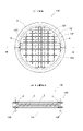
- FIG. 10 is a diagram showing a main part of the probe card 10 according to Embodiment 2 of the present invention, and is a front view and a bottom view of the ST substrate 130.
- FIG. 3A and 3B are a plan view and a cross-sectional view of the ST substrate 130 shown in FIG. 2;
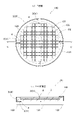
- FIG. 10 is a diagram showing a main part of the probe card 10 according to Embodiment 3 of the present invention, and is a front view and a bottom view of the ST substrate 130.
- FIG. 10 is a diagram showing a main part of the probe card 10 according to Embodiment 3 of the present invention, and is a front view and a bottom view of the ST substrate 130.
- FIG. 5A and 5B are a plan view and a BB cross-sectional view of the ST substrate 130 shown in FIG.
- FIG. 10 is a diagram showing a main part of the probe card 10 according to Embodiment 4 of the present invention, and is a front view and a bottom view of the ST substrate 130.
- FIG. FIG. 7 is a plan view and a CC cross-sectional view of the ST substrate 130 shown in FIG. 6;
- FIG. 10 is a diagram showing a main part of the probe card 10 according to Embodiment 5 of the present invention, and is a front view and a bottom view of the ST substrate 130.
- FIG. FIG. 9 is a plan view and a DD sectional view of the ST substrate 130 shown in FIG. 8;
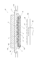
- FIG. 1 is a diagram showing an example of a schematic configuration of a probe card 10 according to Embodiment 1 of the present invention.
- the probe card 10 is attached to the wafer prober with the probe installation surface facing downward, and faces the semiconductor wafer 20 placed on the stage 200. By moving the stage 200 up and down, the probes 15 are moved to the semiconductor wafer. It can be contacted with electrode pads 21 on 20 .
- the probe card 10 is composed of a main substrate 100, a reinforcing plate 110, an interposer 120, an ST (Space Transformer) substrate 130, and two or more probes 15.
- the main board 100 is a wiring board detachably attached to the wafer prober, and for example, a disk-shaped glass epoxy board is used.
- the main substrate 100 is supported by a card holder 210 of a wafer prober at the peripheral portion of the lower surface thereof, and is arranged substantially horizontally.
- a reinforcing plate 110 for suppressing distortion of the main substrate 100 is attached to the central portion of the upper surface of the main substrate 100 .
- Two or more external terminals 11 to which signal terminals of a tester device (not shown) are connected are provided on the upper surface of the main board 100 .
- the interposer 120 is arranged between the main board 100 and the ST board 130, and is a connection means between the boards that conducts the wiring of the main board 100 and the wiring of the ST board 130, and has a large number of pogo pins 12, for example.
- the ST board 130 is an insulating multilayer wiring board, for example, a laminated board in which two or more ceramic plates are stuck together, and is used to convert the electrode pitch.
- the ST board 130 is attached to the main board 100 by the board holder 16 and arranged substantially horizontally.
- the substrate holder 16 has one end fixed to the lower surface of the main substrate 100 and the other end supporting the peripheral portion of the lower surface of the ST substrate 130 .
- Two or more probe electrodes 13 for attaching probes 15 are formed on the lower surface of the ST substrate 130 .
- Two or more pogo-pin electrodes 14 are formed on the upper surface of the ST substrate 130 to contact the pogo-pins 12 of the interposer 120 .
- the probe electrodes 13 are electrically connected to the pogo pin electrodes 14 via the wiring patterns and through holes in the ST substrate 130 , and the probes 15 are electrically connected to the main substrate 100 .
- the probe electrode 13 and the pogo pin electrode 14 are metal films formed by photolithography using an electroplating method or an etching method.
- a heat-generating film 3 is formed on the surface of the ST substrate 130 .
- the probe 15 is made of an elastically deformable conductive metal such as NiCo (nickel-cobalt alloy) and has a tip for contacting the electrode pad 21 .
- NiCo nickel-cobalt alloy
- the stage 200 is a mounting table for the semiconductor wafer 20, and is capable of moving and rotating in the horizontal plane and moving in the vertical direction.
- a heater 201 is a heater for high temperature inspection built in the stage 200 and can heat the semiconductor wafer 20 .
- the heat-generating coating 3 has a composition in which fine carbon particles are mixed with a binder, and is a coating that generates heat when energized.
- the heat-generating coating 3 is formed on the surface of the ST substrate 130 by applying a heat-generating coating material. By energizing the heat generating film 3 before or during the inspection, the temperature of the ST substrate 130 can be maintained at a predetermined inspection temperature during the high temperature inspection.
- the heat-generating coating 3 can be formed on the bottom surface, top surface, or side surface of the ST substrate 130 . Moreover, the heat-generating coating 3 is formed in a region where the probe electrodes 13 and the pogo-pin electrodes 14 are not formed. For example, in the case of forming the heat-generating coating 3 on the lower surface of the ST substrate 130 , it is formed on the periphery of the ST substrate 130 where the probe electrodes 13 are not formed or between adjacent probe electrodes 13 . If the heat-generating coating 3 is formed on the top surface of the ST substrate, it is formed at the periphery of the ST substrate 130 where the pogo-pin electrodes 14 are not formed or between adjacent pogo-pin electrodes 14 .
- the heat-generating coating 3 is connected to a pair of coating electrodes (not shown) and supplied with current flowing through the heat-generating coating 3 .
- the heat-generating coating 3 can be efficiently heated. For example, if the area where the heat-generating coating 3 is formed is rectangular, it is desirable to provide connection electrodes at or near a pair of opposing vertexes, or to provide connection electrodes at or near a pair of opposing sides.
- the heat-generating coating material is a suspension containing a binder-containing solvent or water as a dispersion medium and fine carbon particles as a dispersoid, and is applied to the surface of the ST substrate 130 .
- Polyurethane-based resins, polyolefin-based resins, fluorine-based rubbers, silicone rubbers, and other synthetic resins can be used as binders.
- the dispersion medium is a liquid obtained by dissolving or dispersing such a resin in a solvent or emulsifying it in water.
- the fine carbon particles are powders containing carbon as a main component, and for example, a mixture of graphite and carbon nanotubes can be used.
- Graphite preferably has a particle size of 30 ⁇ m or less, and carbon nanotube preferably has an outer diameter of 1 ⁇ m or less and a length of 50 ⁇ m or less.
- a heat-generating coating material can be obtained by dispersing a mixture of graphite and carbon nanotubes in a solvent in which fluorine-based rubber is dissolved. After the heat-generating coating agent is applied to a predetermined area of the ST substrate 130, the heat-generating coating 3 is formed by evaporating the solvent or water and removing the heat-generating coating agent.
- the heat-generating coating material can be applied to the surface of the ST substrate 130 by spray coating, brush coating, flow dipping, or any other method.
- the heat-generating coating 3 can be formed in any desired region by forming a photoresist in advance on the region where the heat-generating coating 3 is not to be formed and removing the photoresist after the heat-generating coating 3 is formed.
- the heat-generating coating 3 is formed on the conductive member, it is formed with an insulating coating interposed therebetween.
- the heat-generating coating 3 is formed by applying a heat-generating coating material, it can be easily formed in an area where the heating wire that constitutes a conventional heater cannot be formed.
- the heating wire pattern cannot be formed on uneven surfaces, curved or curved surfaces, narrow areas, etc., and conventional heaters cannot be provided.
- the heat-generating coating 3 is formed by coating, the heat-generating coating 3 can be formed even in such a region.
- a heating wire cannot be formed on the peripheral portion or side surface of the ST substrate 130 .
- the periphery is supported by the substrate holder 16 and cannot be circuitized due to manufacturing process reasons.
- the side surface of the ST substrate 130 cannot be formed with a circuit.
- the heat-generating coating 3 can be formed even in such a region.
- the heat-generating coating 3 can be formed in either a wide area or a narrow area. When formed over a wide area, the area can be heated more uniformly than a conventional heater (resistance wire). Moreover, even if a through-hole is provided in a part of a wide area, it can be used as a heating element. Therefore, compared with conventional heaters in which a resistance wire is meandered to cover a wide area, the possibility of failure due to disconnection is low, and reliability can be improved.
- the center of the probe card 10 is easily warmed in the horizontal plane, and the periphery is hard to be warmed. Therefore, by forming the heat-generating coating 3 on the upper and lower surfaces of the ST substrate 130 or on the side surfaces thereof, it is possible to suppress the occurrence of a temperature gradient in the horizontal plane of the ST substrate 130 .
- the present invention is not limited to such a case.
- the heat-generating coating 3 can be formed on the main substrate 100 supporting the probes 15 via the ST substrate 130 and the substrate holder 16 .
- the heat-generating coating 3 can be formed on the reinforcing plate 110 .
- Embodiment 2 In this embodiment, an example of a specific configuration of the heat-generating coating 3 will be described.
- FIGS. 2 and 3(a) to 3(d) are diagrams showing main parts of the probe card 10 according to the second embodiment of the present invention, and show an example of the detailed configuration of the ST board 130 of FIG. ing.
- (a) to (c) in the drawing show a front view, a bottom view, and a plan view of the ST substrate 130, respectively.
- (d) in the drawing shows a cross section (AA cross section) taken along a vertical plane passing through the AA cutting line in (c).
- the ST substrate 130 is divided in a horizontal plane into a circuit area 131 where circuit patterns are formed and a non-circuit area 132 where no circuit patterns are formed.
- the circuit region 131 is a region including the central portion of the ST substrate 130 and is formed apart from the outer peripheral edge 134 of the ST substrate 130 .
- the non-circuit area 132 is an area adjacent to the outer peripheral edge 134 and is an annular area formed outside the circuit area 131 so as to surround the circuit area 131 .
- a boundary line 133 between the circuit area 131 and the non-circuit area 132 extends along the outer peripheral edge 134 of the ST substrate 130.
- the circuit area 131 is inside the boundary line 133, and the non-circuit area 132 is outside the boundary line 133. is.
- the probe electrodes 13 , pogo pin electrodes 14 , and circuit patterns such as through holes and wiring patterns are all formed within the circuit region 131 and not formed within the non-circuit region 132 .
- a probe region 15A in the drawing is a region in which one or more probe electrodes 13 are formed, and a large number of probe regions 15A are formed in a circuit region 131 on the lower surface.
- a pogo pin region 12A in the figure is a region in which one or more pogo pin electrodes 14 are formed, and a large number of pogo pin regions 12A are formed in the circuit region 131 on the upper surface.
- Each heat-generating coating 3 is formed in a region obtained by dividing the non-circuit region 132 in the circumferential direction. That is, two or more heat generating coatings 3 are arranged adjacent to each other in the circumferential direction, and each heat generating coating 3 has an elongated shape extending along the outer peripheral edge 134 .
- the heat-generating coating 3 comprises a body coating 30 for generating heat and a pair of lead coatings 31 for supplying current.
- the body coating 30 has a large area occupying most of the heat-generating coating 3 and is formed within the non-circuit region 132 .
- a pair of lead films 31 are connected to a pair of sides facing each other in the circumferential direction of the body film 30 or in the vicinity thereof, extend across the boundary line 133 to the circuit region 131 , and connect to the film electrode 4 .
- the coating electrode 4 is an electrode terminal for supplying current to the heat generating coating 3 and is formed within the circuit region 131 .
- the coating electrode 4 is electrically connected to the external terminal 11 on the main substrate 100 via the interposer 120 .
- the heater 5 is a well-known heating means, and is composed of a heating wire formed in the circuit area 131 on the lower surface, upper surface, or inner layer of the ST substrate 130 . Heating the circuit area 131 with the heater 5 and heating the non-circuit area 132 with the heat-generating film 3 can suppress the occurrence of a temperature gradient in the horizontal plane of the ST substrate 130 .
- the present invention is not limited to such a case.
- it can be formed only on the lower surface or only on the upper surface.
- the present invention is not limited to such a case, and the heater 5 can be omitted.
- the ST substrate 130 tends to have a lower temperature in the peripheral portion than in the central portion. Therefore, by forming the heat-generating coating 3 in the non-circuit region 132 adjacent to the outer peripheral edge 134, it is possible to suppress the occurrence of a temperature gradient in the horizontal plane of the ST substrate 130.
- FIG. 1 A block diagram illustrating an exemplary computing device.
- heat-generating coatings 3 are formed along the outer peripheral edge 134 , but the present invention is not limited to such a case.
- one or more exothermic coatings 3 can be formed along the outer peripheral edge 134 .
- it is formed in a C-shape in which a portion in the circumferential direction is separated.
- the heat-generating coating 3 is formed in the region adjacent to the outer peripheral edge 134 , but the present invention is not limited to such a case.
- the heat-generating coating 3 can be formed in a region within the non-circuit region 132 and away from the outer peripheral edge 134 .
- Embodiment 3 In the second embodiment, an example of forming the heat-generating coating 3 on the non-circuit region 132 of the ST substrate 130 has been described. In contrast, in the present embodiment, a case where the heat-generating coating 3 is formed not only on the non-circuit area 132 but also on the circuit area 131 will be described.
- FIGS. 4 and 5(a) to 5(d) are diagrams showing main parts of the probe card 10 according to Embodiment 3 of the present invention, and show an example of the detailed configuration of the ST board 130 of FIG. ing.
- (a) to (c) in the drawing show a front view, a bottom view, and a plan view of the ST substrate 130, respectively.
- (d) in the figure shows a cross section (BB cut plane) taken along a vertical plane passing through the BB cut line in (c).
- Components corresponding to those shown in FIGS. 2 and 3 are denoted by the same reference numerals, and overlapping descriptions are omitted.
- the heat-generating coating 3 By forming the heat-generating coating 3 extending along the circumferential direction not only on the non-circuit area 132 of the ST substrate 130 but also on the circuit area 131, the area on the main surface of the ST substrate 130 can be efficiently utilized. can. Therefore, the heat-generating coating 3 can be formed over a wider area and heated effectively.
- Embodiment 4 In the second and third embodiments, examples of forming the heat-generating coating 3 on the lower surface or the upper surface of the ST substrate 130 have been described. In contrast, in the present embodiment, the case where the heat-generating coating 3 is formed on the side surface of the ST substrate 130 will be described.
- FIGS. 6 and 7(a) to 7(d) are diagrams showing essential parts of the probe card 10 according to the fourth embodiment of the present invention, and show an example of the detailed configuration of the ST board 130 of FIG. ing.
- (a) to (c) in the drawing show a front view, a bottom view, and a plan view of the ST substrate 130, respectively.
- (d) in the figure shows a cross section (CC cutting plane) taken along a vertical plane passing through the CC cutting line in (c).
- Components corresponding to those shown in FIGS. 2 to 5 are denoted by the same reference numerals, and overlapping descriptions are omitted.
- the heat-generating coating 3 comprises a body coating 30 for generating heat and a pair of lead coatings 31 for supplying current.
- the body coating 30 has a large area occupying most of the heat-generating coating 3 and is formed on the side surface of the ST substrate 130 .
- a pair of lead films 31 are formed on the main surface of the ST substrate 130 , one end of which is connected to a pair of sides facing each other in the circumferential direction of the body film 30 or their vicinity, and the other end of which is connected to the boundary line 133 . It extends across to the circuit area 131 and is connected to the coating electrode 4 .
- one of the pair of coating electrodes 4 is formed on the lower surface and the other is formed on the upper surface. Therefore, one of the pair of lead films 31 is formed on the lower surface and the other is formed on the upper surface.
- the pair of lead coatings 31 can be connected to or near a pair of vertices facing each other in the diagonal direction of the body coating 30 having a substantially rectangular shape, and the body coating 30 can be connected to substantially the entire body coating 30 . can be used to effectively generate heat.
- Embodiment 5 In the fourth embodiment, an example in which the heat-generating coating 3 is formed on the side surface of the ST substrate 130 has been described. On the other hand, in the present embodiment, a case where the heat generating film 3 is formed not only on the side surface of the ST substrate 130 but also on the non-circuit area 132 on the main surface of the ST substrate 130 will be described.
- FIGS. 8 and 9(a) to 9(d) are diagrams showing main parts of the probe card 10 according to Embodiment 5 of the present invention, and show an example of the detailed configuration of the ST board 130 of FIG. ing.
- (a) to (c) in the drawing show a front view, a bottom view, and a plan view of the ST substrate 130, respectively.
- (d) in the figure shows a cross section (DD cut plane) taken along a vertical plane passing through the DD cut line of (c).
- Components corresponding to those shown in FIGS. 2 to 7 are denoted by the same reference numerals, and overlapping descriptions are omitted.
- the heat-generating coating 3 is formed across the outer peripheral edge 134 of the lower surface and the outer peripheral edge 134 of the upper surface, , the lower surface and the upper surface are also formed to extend along the circumferential direction. Furthermore, the heat-generating coatings 3 formed on the upper and lower surfaces are formed across the boundary line 133 and are formed to extend in the circumferential direction not only in the non-circuit area 132 but also in the circuit area 131 . Therefore, the heat generating coating 3 is also different in that it is connected to the coating electrode 4 without having the lead coating 31 .
- the heat-generating film 3 is formed not only on the side surface of the ST substrate 130 but also on the non-circuit area 132 on the main surface, and by heating both the side surface and the non-circuit area 132, the empty space on the ST substrate 130 is effectively utilized. can be heated by In addition, by forming the heating element not only in the non-circuit area 132 but also in the circuit area 131 and heating the circuit area 131, the empty space on the ST substrate 130 can be further effectively utilized for heating. Therefore, the heat-generating coating 3 can be formed over a wider area and the ST substrate 130 can be effectively heated.
- a pair of coating electrodes 4 are arranged at or near vertexes of the exothermic coating 3 facing diagonally. That is, one film electrode 4 is formed in the circuit region 131 on the lower surface of the ST substrate 130 , and the other film electrode 4 is formed in the circuit region 131 on the upper surface of the ST substrate 130 .
- these coating electrodes 4 are connected in the vicinity of a pair of opposite sides of the heat generating coating 3 in the circumferential direction. Therefore, heat can be effectively generated by using substantially the entire heat-generating coating 3 .
- Heat-generating coating 4 Coating electrode (electrode terminal) 5 heater 10 probe card 11 external terminal 12 pogo pin 12A pogo pin area 13 probe electrode 14 pogo pin electrode 15 probe 15A probe area 16 substrate holder 20 semiconductor wafer 21 electrode pad 30 body coating 31 lead coating 100 main substrate 110 reinforcing plate 120 interposer 130 ST substrate 131 Circuit area 132 Non-circuit area 133 Boundary line 134 Outer peripheral edge 200 Stage 201 Heater 210 Card holder
Landscapes
- Engineering & Computer Science (AREA)
- General Physics & Mathematics (AREA)
- Physics & Mathematics (AREA)
- Environmental & Geological Engineering (AREA)
- Computer Hardware Design (AREA)
- Microelectronics & Electronic Packaging (AREA)
- Toxicology (AREA)
- Health & Medical Sciences (AREA)
- General Engineering & Computer Science (AREA)
- Manufacturing & Machinery (AREA)
- Power Engineering (AREA)
- Testing Or Measuring Of Semiconductors Or The Like (AREA)
- Measuring Leads Or Probes (AREA)
Abstract
Priority Applications (7)
| Application Number | Priority Date | Filing Date | Title |
|---|---|---|---|
| KR1020237015422A KR20230082670A (ko) | 2021-03-15 | 2021-03-15 | 프로브 카드 |
| JP2023506376A JPWO2022195648A1 (fr) | 2021-03-15 | 2021-03-15 | |
| PCT/JP2021/010294 WO2022195648A1 (fr) | 2021-03-15 | 2021-03-15 | Carte sonde |
| US18/265,264 US20240044942A1 (en) | 2021-03-15 | 2021-03-15 | Probe card |
| CN202180077519.8A CN116547543A (zh) | 2021-03-15 | 2021-03-15 | 探针卡 |
| TW111148732A TW202314258A (zh) | 2021-03-15 | 2021-12-13 | 探針卡 |
| TW110146541A TWI795122B (zh) | 2021-03-15 | 2021-12-13 | 探針卡 |
Applications Claiming Priority (1)
| Application Number | Priority Date | Filing Date | Title |
|---|---|---|---|
| PCT/JP2021/010294 WO2022195648A1 (fr) | 2021-03-15 | 2021-03-15 | Carte sonde |
Publications (1)
| Publication Number | Publication Date |
|---|---|
| WO2022195648A1 true WO2022195648A1 (fr) | 2022-09-22 |
Family
ID=83320040
Family Applications (1)
| Application Number | Title | Priority Date | Filing Date |
|---|---|---|---|
| PCT/JP2021/010294 WO2022195648A1 (fr) | 2021-03-15 | 2021-03-15 | Carte sonde |
Country Status (6)
| Country | Link |
|---|---|
| US (1) | US20240044942A1 (fr) |
| JP (1) | JPWO2022195648A1 (fr) |
| KR (1) | KR20230082670A (fr) |
| CN (1) | CN116547543A (fr) |
| TW (2) | TW202314258A (fr) |
| WO (1) | WO2022195648A1 (fr) |
Citations (2)
| Publication number | Priority date | Publication date | Assignee | Title |
|---|---|---|---|---|
| JP2000346875A (ja) * | 1999-06-07 | 2000-12-15 | Advantest Corp | プローブカードおよびこれを用いたic試験装置 |
| JP2002532822A (ja) * | 1998-12-04 | 2002-10-02 | ピージェイオー(インディサーム)リミテッド | 導電性材料 |
Family Cites Families (1)
| Publication number | Priority date | Publication date | Assignee | Title |
|---|---|---|---|---|
| TWM587275U (zh) * | 2018-12-04 | 2019-12-01 | 蔚華科技股份有限公司 | 測試半導體設備之結構 |
-
2021
- 2021-03-15 KR KR1020237015422A patent/KR20230082670A/ko unknown
- 2021-03-15 CN CN202180077519.8A patent/CN116547543A/zh active Pending
- 2021-03-15 JP JP2023506376A patent/JPWO2022195648A1/ja active Pending
- 2021-03-15 WO PCT/JP2021/010294 patent/WO2022195648A1/fr active Application Filing
- 2021-03-15 US US18/265,264 patent/US20240044942A1/en active Pending
- 2021-12-13 TW TW111148732A patent/TW202314258A/zh unknown
- 2021-12-13 TW TW110146541A patent/TWI795122B/zh active
Patent Citations (2)
| Publication number | Priority date | Publication date | Assignee | Title |
|---|---|---|---|---|
| JP2002532822A (ja) * | 1998-12-04 | 2002-10-02 | ピージェイオー(インディサーム)リミテッド | 導電性材料 |
| JP2000346875A (ja) * | 1999-06-07 | 2000-12-15 | Advantest Corp | プローブカードおよびこれを用いたic試験装置 |
Also Published As
| Publication number | Publication date |
|---|---|
| TW202314258A (zh) | 2023-04-01 |
| JPWO2022195648A1 (fr) | 2022-09-22 |
| TW202238152A (zh) | 2022-10-01 |
| TWI795122B (zh) | 2023-03-01 |
| US20240044942A1 (en) | 2024-02-08 |
| CN116547543A (zh) | 2023-08-04 |
| KR20230082670A (ko) | 2023-06-08 |
Similar Documents
| Publication | Publication Date | Title |
|---|---|---|
| JP3685192B2 (ja) | 異方導電性コネクターおよび導電性ペースト組成物、プローブ部材並びにウエハ検査装置およびウエハ検査方法 | |
| TWI239404B (en) | Anisotropic conductive connector and electrically conductive paste constitution, probe member, wafer inspection apparatus and wafer inspection method | |
| TWI430525B (zh) | An aisotropic conductive connector, a probe member, and a wafer inspection device | |
| KR20050027252A (ko) | 이방 도전성 커넥터 및 프로우브 부재 및 웨이퍼 검사장치 및 웨이퍼 검사 방법 | |
| JP2007085833A (ja) | ウエハ検査用異方導電性コネクターおよびその製造方法、ウエハ検査用プローブカード並びにウエハ検査装置 | |
| JP2004342597A (ja) | 異方導電性シートおよびその製造方法、アダプター装置およびその製造方法並びに回路装置の電気的検査装置 | |
| CN103841759B (zh) | 多层布线板及其制造方法 | |
| JP3573120B2 (ja) | 異方導電性コネクターおよびその製造方法並びにその応用製品 | |
| CN100359659C (zh) | 各向异性导电连接器、探测部件和晶片检测设备以及晶片检测方法 | |
| WO2022195648A1 (fr) | Carte sonde | |
| JP5079806B2 (ja) | 検査用構造体 | |
| TW200848746A (en) | Sheet-like probe and method for manufacturing the same | |
| JP5104265B2 (ja) | プローブ部材およびその製造方法ならびにその応用 | |
| JP3649245B2 (ja) | シート状プローブの製造方法 | |
| JP7393873B2 (ja) | 電気的接触子及びプローブカード | |
| JP2009098065A (ja) | プローブ部材およびその製造方法ならびにその応用 | |
| JP3938117B2 (ja) | 異方導電性コネクターおよびプローブ部材並びにウエハ検査装置およびウエハ検査方法 | |
| JP2006284418A (ja) | ウエハ検査用プローブカードおよびウエハ検査装置 | |
| JP3781048B2 (ja) | シート状プローブおよびその応用 | |
| JP2009222495A (ja) | ウエハ検査装置 | |
| JP2006216502A (ja) | 異方導電性コネクター、プローブカード並びにウエハ検査装置およびウエハ検査方法 | |
| JP2005037229A (ja) | 電気的接続装置 | |
| JP2009047565A (ja) | シート状プローブおよびその製造方法 | |
| JP2004096107A (ja) | 異方導電性コネクターおよび導電性ペースト組成物、プローブ部材並びにウエハ検査装置およびウエハ検査方法 | |
| KR20220127584A (ko) | 컨택터 어레이 및 그 제조 방법 |
Legal Events
| Date | Code | Title | Description |
|---|---|---|---|
| 121 | Ep: the epo has been informed by wipo that ep was designated in this application |
Ref document number: 21931404 Country of ref document: EP Kind code of ref document: A1 |
|
| ENP | Entry into the national phase |
Ref document number: 2023506376 Country of ref document: JP Kind code of ref document: A |
|
| ENP | Entry into the national phase |
Ref document number: 20237015422 Country of ref document: KR Kind code of ref document: A |
|
| WWE | Wipo information: entry into national phase |
Ref document number: 202180077519.8 Country of ref document: CN |
|
| WWE | Wipo information: entry into national phase |
Ref document number: 18265264 Country of ref document: US |
|
| WWE | Wipo information: entry into national phase |
Ref document number: 11202304274P Country of ref document: SG |
|
| NENP | Non-entry into the national phase |
Ref country code: DE |
|
| 122 | Ep: pct application non-entry in european phase |
Ref document number: 21931404 Country of ref document: EP Kind code of ref document: A1 |