WO2022190275A1 - 半導体レーザ装置 - Google Patents
半導体レーザ装置 Download PDFInfo
- Publication number
- WO2022190275A1 WO2022190275A1 PCT/JP2021/009586 JP2021009586W WO2022190275A1 WO 2022190275 A1 WO2022190275 A1 WO 2022190275A1 JP 2021009586 W JP2021009586 W JP 2021009586W WO 2022190275 A1 WO2022190275 A1 WO 2022190275A1
- Authority
- WO
- WIPO (PCT)
- Prior art keywords
- region
- ridge
- layer
- current
- conductivity type
- Prior art date
- Legal status (The legal status is an assumption and is not a legal conclusion. Google has not performed a legal analysis and makes no representation as to the accuracy of the status listed.)
- Ceased
Links
Images






Classifications
-
- H—ELECTRICITY
- H01—ELECTRIC ELEMENTS
- H01S—DEVICES USING THE PROCESS OF LIGHT AMPLIFICATION BY STIMULATED EMISSION OF RADIATION [LASER] TO AMPLIFY OR GENERATE LIGHT; DEVICES USING STIMULATED EMISSION OF ELECTROMAGNETIC RADIATION IN WAVE RANGES OTHER THAN OPTICAL
- H01S5/00—Semiconductor lasers
- H01S5/20—Structure or shape of the semiconductor body to guide the optical wave ; Confining structures perpendicular to the optical axis, e.g. index or gain guiding, stripe geometry, broad area lasers, gain tailoring, transverse or lateral reflectors, special cladding structures, MQW barrier reflection layers
- H01S5/22—Structure or shape of the semiconductor body to guide the optical wave ; Confining structures perpendicular to the optical axis, e.g. index or gain guiding, stripe geometry, broad area lasers, gain tailoring, transverse or lateral reflectors, special cladding structures, MQW barrier reflection layers having a ridge or stripe structure
- H01S5/2205—Structure or shape of the semiconductor body to guide the optical wave ; Confining structures perpendicular to the optical axis, e.g. index or gain guiding, stripe geometry, broad area lasers, gain tailoring, transverse or lateral reflectors, special cladding structures, MQW barrier reflection layers having a ridge or stripe structure comprising special burying or current confinement layers
- H01S5/2218—Structure or shape of the semiconductor body to guide the optical wave ; Confining structures perpendicular to the optical axis, e.g. index or gain guiding, stripe geometry, broad area lasers, gain tailoring, transverse or lateral reflectors, special cladding structures, MQW barrier reflection layers having a ridge or stripe structure comprising special burying or current confinement layers having special optical properties
-
- H—ELECTRICITY
- H01—ELECTRIC ELEMENTS
- H01S—DEVICES USING THE PROCESS OF LIGHT AMPLIFICATION BY STIMULATED EMISSION OF RADIATION [LASER] TO AMPLIFY OR GENERATE LIGHT; DEVICES USING STIMULATED EMISSION OF ELECTROMAGNETIC RADIATION IN WAVE RANGES OTHER THAN OPTICAL
- H01S5/00—Semiconductor lasers
- H01S5/10—Construction or shape of the optical resonator, e.g. extended or external cavity, coupled cavities, bent-guide, varying width, thickness or composition of the active region
- H01S5/1003—Waveguide having a modified shape along the axis, e.g. branched, curved, tapered, voids
- H01S5/1014—Tapered waveguide, e.g. spotsize converter
-
- H—ELECTRICITY
- H01—ELECTRIC ELEMENTS
- H01S—DEVICES USING THE PROCESS OF LIGHT AMPLIFICATION BY STIMULATED EMISSION OF RADIATION [LASER] TO AMPLIFY OR GENERATE LIGHT; DEVICES USING STIMULATED EMISSION OF ELECTROMAGNETIC RADIATION IN WAVE RANGES OTHER THAN OPTICAL
- H01S5/00—Semiconductor lasers
- H01S5/20—Structure or shape of the semiconductor body to guide the optical wave ; Confining structures perpendicular to the optical axis, e.g. index or gain guiding, stripe geometry, broad area lasers, gain tailoring, transverse or lateral reflectors, special cladding structures, MQW barrier reflection layers
- H01S5/2004—Confining in the direction perpendicular to the layer structure
- H01S5/2018—Optical confinement, e.g. absorbing-, reflecting- or waveguide-layers
- H01S5/2031—Optical confinement, e.g. absorbing-, reflecting- or waveguide-layers characterized by special waveguide layers, e.g. asymmetric waveguide layers or defined bandgap discontinuities
-
- H—ELECTRICITY
- H01—ELECTRIC ELEMENTS
- H01S—DEVICES USING THE PROCESS OF LIGHT AMPLIFICATION BY STIMULATED EMISSION OF RADIATION [LASER] TO AMPLIFY OR GENERATE LIGHT; DEVICES USING STIMULATED EMISSION OF ELECTROMAGNETIC RADIATION IN WAVE RANGES OTHER THAN OPTICAL
- H01S5/00—Semiconductor lasers
- H01S5/20—Structure or shape of the semiconductor body to guide the optical wave ; Confining structures perpendicular to the optical axis, e.g. index or gain guiding, stripe geometry, broad area lasers, gain tailoring, transverse or lateral reflectors, special cladding structures, MQW barrier reflection layers
- H01S5/2036—Broad area lasers
-
- H—ELECTRICITY
- H01—ELECTRIC ELEMENTS
- H01S—DEVICES USING THE PROCESS OF LIGHT AMPLIFICATION BY STIMULATED EMISSION OF RADIATION [LASER] TO AMPLIFY OR GENERATE LIGHT; DEVICES USING STIMULATED EMISSION OF ELECTROMAGNETIC RADIATION IN WAVE RANGES OTHER THAN OPTICAL
- H01S5/00—Semiconductor lasers
- H01S5/20—Structure or shape of the semiconductor body to guide the optical wave ; Confining structures perpendicular to the optical axis, e.g. index or gain guiding, stripe geometry, broad area lasers, gain tailoring, transverse or lateral reflectors, special cladding structures, MQW barrier reflection layers
- H01S5/22—Structure or shape of the semiconductor body to guide the optical wave ; Confining structures perpendicular to the optical axis, e.g. index or gain guiding, stripe geometry, broad area lasers, gain tailoring, transverse or lateral reflectors, special cladding structures, MQW barrier reflection layers having a ridge or stripe structure
-
- H—ELECTRICITY
- H01—ELECTRIC ELEMENTS
- H01S—DEVICES USING THE PROCESS OF LIGHT AMPLIFICATION BY STIMULATED EMISSION OF RADIATION [LASER] TO AMPLIFY OR GENERATE LIGHT; DEVICES USING STIMULATED EMISSION OF ELECTROMAGNETIC RADIATION IN WAVE RANGES OTHER THAN OPTICAL
- H01S2301/00—Functional characteristics
- H01S2301/16—Semiconductor lasers with special structural design to influence the modes, e.g. specific multimode
- H01S2301/166—Single transverse or lateral mode
-
- H—ELECTRICITY
- H01—ELECTRIC ELEMENTS
- H01S—DEVICES USING THE PROCESS OF LIGHT AMPLIFICATION BY STIMULATED EMISSION OF RADIATION [LASER] TO AMPLIFY OR GENERATE LIGHT; DEVICES USING STIMULATED EMISSION OF ELECTROMAGNETIC RADIATION IN WAVE RANGES OTHER THAN OPTICAL
- H01S2301/00—Functional characteristics
- H01S2301/18—Semiconductor lasers with special structural design for influencing the near- or far-field
-
- H—ELECTRICITY
- H01—ELECTRIC ELEMENTS
- H01S—DEVICES USING THE PROCESS OF LIGHT AMPLIFICATION BY STIMULATED EMISSION OF RADIATION [LASER] TO AMPLIFY OR GENERATE LIGHT; DEVICES USING STIMULATED EMISSION OF ELECTROMAGNETIC RADIATION IN WAVE RANGES OTHER THAN OPTICAL
- H01S5/00—Semiconductor lasers
- H01S5/04—Processes or apparatus for excitation, e.g. pumping, e.g. by electron beams
- H01S5/042—Electrical excitation ; Circuits therefor
- H01S5/0425—Electrodes, e.g. characterised by the structure
- H01S5/04254—Electrodes, e.g. characterised by the structure characterised by the shape
-
- H—ELECTRICITY
- H01—ELECTRIC ELEMENTS
- H01S—DEVICES USING THE PROCESS OF LIGHT AMPLIFICATION BY STIMULATED EMISSION OF RADIATION [LASER] TO AMPLIFY OR GENERATE LIGHT; DEVICES USING STIMULATED EMISSION OF ELECTROMAGNETIC RADIATION IN WAVE RANGES OTHER THAN OPTICAL
- H01S5/00—Semiconductor lasers
- H01S5/20—Structure or shape of the semiconductor body to guide the optical wave ; Confining structures perpendicular to the optical axis, e.g. index or gain guiding, stripe geometry, broad area lasers, gain tailoring, transverse or lateral reflectors, special cladding structures, MQW barrier reflection layers
- H01S5/2054—Methods of obtaining the confinement
- H01S5/2059—Methods of obtaining the confinement by means of particular conductivity zones, e.g. obtained by particle bombardment or diffusion
- H01S5/2063—Methods of obtaining the confinement by means of particular conductivity zones, e.g. obtained by particle bombardment or diffusion obtained by particle bombardment
-
- H—ELECTRICITY
- H01—ELECTRIC ELEMENTS
- H01S—DEVICES USING THE PROCESS OF LIGHT AMPLIFICATION BY STIMULATED EMISSION OF RADIATION [LASER] TO AMPLIFY OR GENERATE LIGHT; DEVICES USING STIMULATED EMISSION OF ELECTROMAGNETIC RADIATION IN WAVE RANGES OTHER THAN OPTICAL
- H01S5/00—Semiconductor lasers
- H01S5/20—Structure or shape of the semiconductor body to guide the optical wave ; Confining structures perpendicular to the optical axis, e.g. index or gain guiding, stripe geometry, broad area lasers, gain tailoring, transverse or lateral reflectors, special cladding structures, MQW barrier reflection layers
- H01S5/2054—Methods of obtaining the confinement
- H01S5/2081—Methods of obtaining the confinement using special etching techniques
- H01S5/209—Methods of obtaining the confinement using special etching techniques special etch stop layers
-
- H—ELECTRICITY
- H01—ELECTRIC ELEMENTS
- H01S—DEVICES USING THE PROCESS OF LIGHT AMPLIFICATION BY STIMULATED EMISSION OF RADIATION [LASER] TO AMPLIFY OR GENERATE LIGHT; DEVICES USING STIMULATED EMISSION OF ELECTROMAGNETIC RADIATION IN WAVE RANGES OTHER THAN OPTICAL
- H01S5/00—Semiconductor lasers
- H01S5/30—Structure or shape of the active region; Materials used for the active region
- H01S5/34—Structure or shape of the active region; Materials used for the active region comprising quantum well or superlattice structures, e.g. single quantum well [SQW] lasers, multiple quantum well [MQW] lasers or graded index separate confinement heterostructure [GRINSCH] lasers
- H01S5/343—Structure or shape of the active region; Materials used for the active region comprising quantum well or superlattice structures, e.g. single quantum well [SQW] lasers, multiple quantum well [MQW] lasers or graded index separate confinement heterostructure [GRINSCH] lasers in AIIIBV compounds, e.g. AlGaAs-laser, InP-based laser
- H01S5/34313—Structure or shape of the active region; Materials used for the active region comprising quantum well or superlattice structures, e.g. single quantum well [SQW] lasers, multiple quantum well [MQW] lasers or graded index separate confinement heterostructure [GRINSCH] lasers in AIIIBV compounds, e.g. AlGaAs-laser, InP-based laser with a well layer having only As as V-compound, e.g. AlGaAs, InGaAs
Definitions
- the present disclosure relates to a semiconductor laser device.
- Patent Document 1 discloses a ridge-type broad area semiconductor laser device having an actual refractive index distribution in the horizontal direction.
- the allowable mode number in the horizontal direction is disclosed to reduce the horizontal spread angle.
- the actual refractive index distribution means a refractive index distribution in which the refractive index is described by a real number
- the waveguide mechanism is a refractive index waveguide, and the electric field distribution, magnetic field distribution, and propagation distribution obtained by solving the wave equation Constants are real numbers.
- Patent Document 2 in a ridge type broad area semiconductor laser device in which a refractive index difference is provided in the horizontal direction by embedding semiconductor layers on both sides of the ridge, current is not injected into the ridge side of the boundary between the ridge and the semiconductor layer. It is disclosed that the current non-injection width is preferably 10 ⁇ m or less in order to suppress the peak of the near field pattern (NFP) appearing near both ends of the ridge and to suppress the increase in loss.
- NFP near field pattern
- Patent Document 3 discloses that, in a ridge structure with a ridge width of 30 ⁇ m that allows higher-order modes, protons are implanted to a depth of 1.6 ⁇ m from the surface of the ridge to the bottom of the ridge leaving a central portion with a width of 15 ⁇ m.
- a ridge-type broad area semiconductor laser device that selectively oscillates the fundamental mode by providing a high-resistance proton-implanted region and passing current through the central portion of the ridge structure with a width of 15 ⁇ m to increase the gain of the fundamental mode. It is
- the NFP in the vicinity of both ends of the ridge does not show a peak.
- the NFP at the site was not weakened. This is because, in the case of a ridge-type broad area semiconductor laser device having a real refractive index distribution, the NFP is determined by the linear coupling of each allowed mode, and if the current is locally reduced, all modes are affected.
- the peculiar phenomenon occurring in the broad area semiconductor laser device embedded in the semiconductor layer is considered to occur when the buried semiconductor layer becomes a gain waveguide or a loss waveguide. Therefore, the structure embedded with a semiconductor layer has not been applied to a ridge type broad area semiconductor laser device having a real refractive index distribution.
- the proton injection for the purpose of increasing the resistance in the conventional ridge-type broad area semiconductor laser device was performed until it reached the bottom of the ridge, the light generated in the active layer spread to the proton injection region. Since the proton injection destroys the crystallinity of the crystal layer, the light that spreads to the proton injection region is scattered by the crystal defects and suffers a large loss. As a result, the slope efficiency is lowered, and the power conversion efficiency is lowered. Furthermore, since the proton injection region in which many crystal defects exist is close to the active layer, there is a problem that the reliability of the broad area semiconductor laser device is remarkably lowered due to the crystal defects in the proton injection region.
- An object of the present invention is to obtain a ridge-type broad area semiconductor laser device that maintains high power conversion efficiency and achieves high reliability by suppressing an increase in operating voltage and an increase in scattering loss caused by crystal defects.
- a semiconductor laser device includes a semiconductor substrate of a first conductivity type, a clad layer of the first conductivity type sequentially laminated on the semiconductor substrate of the first conductivity type, an optical guide layer on the side of the first conductivity type, an active layer, and an active layer. layer, a second-conductivity-type optical guide layer, a second-conductivity-type clad layer, a second-conductivity-type contact layer, and a front end surface and a rear end surface for reciprocating laser light, and having a length of Lc .
- the resonator comprises a current confinement region having a length of L f and a current injection region having a length of L c ⁇ L f , wherein the current confinement
- the regions are a ridge inner region with a width of 2W i and an effective refractive index of n a i , and a region on each side of said ridge inner region with a width of W o and an effective refractive index of na o .
- n c is the average refractive index n a e of the ridge inner region and the ridge outer region, where: and satisfies the following relationship,
- the number of modes allowed in the current confinement region in the ridge width direction is m (an integer equal to or greater than 2), and the width Wo of the ridge outer region is the distance from the lower end of the current non-injection structure to the active layer.
- the current injection region comprises the ridge region having an effective refractive index of na, which is a real number, and a width of 2W in the ridge width direction, and the cladding regions provided on both sides of the ridge region. and the number of modes allowed in the ridge width direction of the current injection region is the same as the number of modes allowed in the current confinement region, and the length of the current confinement region is L f It has a structure that is longer than zero and shorter than the resonator length Lc .
- a current non-injection structure that is, a current confinement region is provided in a part of the interior of the resonator, and a current injection region is provided in the remaining part of the resonator.
- the gain of the low-order mode becomes higher than the gain of the high-order mode, enabling laser oscillation in the low-order mode and narrowing the horizontal divergence angle. Since the electrical resistance is smaller than in the structure in which .
- FIG. 4 is a schematic diagram showing current flow and refractive index distribution in a cross section of a ridge type broad area semiconductor laser device having a real refractive index distribution of a comparative example and a current injection region of the present disclosure
- FIG. 2 is a schematic diagram showing current flow and refractive index distribution in a cross section of a current confinement region of a ridge-type broad area semiconductor laser device having a real refractive index distribution according to the present disclosure
- 1A and 1B are a perspective view and a cross-sectional view showing a 975 nm band ridge-type broad area semiconductor laser device having a real refractive index distribution according to a first embodiment;
- FIG. 4 is a schematic diagram showing current flow and refractive index distribution in a cross section of a ridge type broad area semiconductor laser device having a real refractive index distribution of a comparative example and a current injection region of the present disclosure
- FIG. 2 is a schematic diagram showing current flow and refractive index distribution in a cross section of
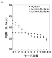
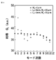
- FIG. 3 is a diagram showing the gain of each mode of the 975 nm band ridge-type broad area semiconductor laser device having the actual refractive index distribution according to the first embodiment;
- FIG. 3 is a diagram showing the gain of each mode of the 975 nm band ridge-type broad area semiconductor laser device having the actual refractive index distribution according to the first embodiment;
- FIG. 3 is a diagram showing the gain of each mode of the 975 nm band ridge-type broad area semiconductor laser device having the actual refractive index distribution according to the first embodiment;
- 8A and 8B are a perspective view and a cross-sectional view showing a 975 nm band ridge type broad area semiconductor laser device having a real refractive index distribution according to a second embodiment;
- FIG. 10 is a diagram showing the gain of each mode of the 975 nm band ridge type broad area semiconductor laser device having the actual refractive index distribution according to the second embodiment;
- FIG. 10 is a diagram showing the gain of each mode of the 975 nm band ridge type broad area semiconductor laser device having the actual refractive index distribution according to the second embodiment;
- FIG. 10 is a diagram showing the gain of each mode of the 975 nm band ridge type broad area semiconductor laser device having the actual refractive index distribution according to the second embodiment;
- 13A and 13B are a perspective view and a cross-sectional view showing a 975 nm band ridge type broad area semiconductor laser device having a real refractive index distribution according to a third embodiment;
- FIG. 10 is a diagram showing gains of respective modes of a 975 nm band ridge-type broad area semiconductor laser device having a real refractive index distribution according to Embodiment 3;
- FIG. 10 is a diagram showing gains of respective modes of a 975 nm band ridge-type broad area semiconductor laser device having a real refractive index distribution according to Embodiment 3;
- FIG. 10 is a diagram showing gains of respective modes of a 975 nm band ridge-type broad area semiconductor laser device having a real refractive index distribution according to Embodiment 3;
- FIG. 10 is a diagram showing gains of respective modes of a 975 nm band ridge-type broad area semiconductor laser device having a real refractive index distribution according to Embodiment 3; 13A and 13B are a perspective view and a cross-sectional view showing a 975 nm band ridge type broad area semiconductor laser device having a real refractive index distribution according to a fourth embodiment; 13A and 13B are a perspective view and a cross-sectional view showing a 975 nm band ridge type broad area semiconductor laser device having a real refractive index distribution according to a fifth embodiment; 14A and 14B are a perspective view and a cross-sectional view showing a 975 nm band ridge type broad area semiconductor laser device having a real refractive index distribution according to a sixth embodiment;
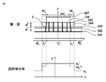
- FIG. 1 is a schematic diagram showing current flow and refractive index distribution in a cross section of a current injection region in a ridge type broad area semiconductor laser device having an actual refractive index distribution as a comparative example and a ridge type broad area semiconductor laser device of the present disclosure.
- FIG. 2 is a schematic diagram showing the current flow and refractive index distribution in the cross section of the current confinement region of the ridge type broad area semiconductor laser device having the actual refractive index distribution according to the present disclosure.
- an active layer 101 from the lower semiconductor substrate (not shown) side, an active layer 101, a guide layer 102, a first etching stop layer 103 (first ESL layer, Etching Stop Layer: ESL), and a p-type first clad layer 104 , a second etching stop layer 105 (second ESL layer), a p-type second cladding layer 106, and a p-type contact layer 107 are shown.
- the current I flowing through the ridge region (I a ) flows from the top end of the first ESL layer 103 in the horizontal direction (x-axis direction). It will also spread and flow.
- the current distribution J(x) at the upper end of the active layer 101 can be calculated using Non-Patent Document 1. Note that the x-axis direction may also be referred to as the ridge width direction.
- a ridge region (I a ) having a ridge region width of 2W is sandwiched between cladding regions (II c ).
- the effective refractive indices of the ridge region (I a ) and cladding region (II c ) are denoted by n a and n c respectively.
- the normalized frequency v can be defined by the following equation (1).
- ⁇ is the oscillation wavelength of the semiconductor laser.
- INT[v/( ⁇ /2)]+1 which is the number obtained by dividing the normalized frequency v by ⁇ /2, making it an integer, and adding 1, is the number of modes allowed in the x direction.
- FIG. 2 shows the current I in the cross section orthogonal to the optical waveguide direction in the current confinement region (C n ) having the current non-injection structure in the ridge type broad area semiconductor laser device having the actual refractive index distribution disclosed in the present application.
- It is a schematic diagram which shows a flow and refractive index distribution.
- the effective refractive index of the ridge outer region (I ao ) of width W o (hereinafter referred to as ridge outer region width) is determined by the ridge inner region (I a i ) of width 2W i (hereinafter referred to as ridge inner region width).
- the structure is such that a portion from the p-type contact layer 107 on the surface to the upper end portion of the second ESL layer 105 is removed by etching within a range substantially equal to the effective refractive index of .
- the current I flows exclusively through the ridge inner region (I a i ). .
- the current I begins to spread horizontally from the top end of the second ESL layer 105 and passes through a distance of h1 + h2. It reaches the active layer 101 .
- the distance h 1 +h 2 over which the current I spreads is longer than the distance h 1 over which the current I spreads in the structure of the comparative example. current spread is narrower in the structure of the present disclosure.
- the current injection region (C i ) in the region in which the current non-injection structure is not provided, that is, the current injection region (C i ), similar to the structure of the comparative example shown in FIG. Current spreads in the horizontal (x) direction from the top of the first ESL layer 103 .
- ⁇ i (x) be the i-th mode allowed in the horizontal direction, and normalize as in the following equation (3). Note that the allowable mode ⁇ i (x) can be calculated from Non-Patent Document 2 or the like.
- the gain G i when light makes one round trip in the resonator is defined by the following equation (5). Since both the light intensity distribution (mode) and the current distribution are normalized, the difference in the gain of each mode can be found from the magnitude relationship of the gain Gi .
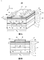
- FIG. 3A is a perspective view showing a 975 nm band ridge type broad area semiconductor laser device 100 having a real refractive index distribution according to Embodiment 1.
- FIG. 3B is a cross-sectional view of the current injection region (C i ) of the ridge type broad area semiconductor laser device 100, that is, a cross-sectional view taken along line AA in FIG. 3A.
- an xyz orthogonal coordinate system is defined for convenience of explanation.
- the x-axis is an axis perpendicular to the yz-plane and coincides with the width direction axis of the ridge type broad area semiconductor laser device 100 .
- the x-axis direction is also called the "ridge width direction”.
- a horizontal transverse mode occurs in the ridge-type broad area semiconductor laser device 100 along the x-axis.
- the y-axis direction coincides with the crystal growth direction of each semiconductor layer formed on the n-type GaAs substrate 2 .
- the y-axis direction is also called a "stacking direction".
- the y-axis is assumed to be parallel to the normal to the top surface of the n-type GaAs substrate 2 .
- the z-axis is the direction in which the ridge-type broad-area semiconductor laser device 100 emits laser light, and is also the longitudinal axis of the resonator of the ridge-type broad-area semiconductor laser device 100 .
- the z-direction is also called the "resonator direction”.
- the ridge type broad area semiconductor laser device 100 includes, from the bottom side (also referred to as the back side), an n-type electrode 1 (first conductivity type electrode), an n-type GaAs substrate 2 (first conductivity type semiconductor substrate), an n-type AlGaAs clad layer 3 with an Al composition ratio of 0.20 and a layer thickness of 1.5 ⁇ m (first conductivity type clad layer, refractive index n cn ), an Al composition ratio of 0.25 and a layer thickness of d ln 200 nm n-type AlGaAs low refractive index layer 4 (refractive index n ln ), Al composition ratio 0.16 and layer thickness dg 2n of 1050 nm n-side AlGaAs second optical guide layer 5 (refractive index n g2n ), Al composition The n-side AlGaAs first optical guide layer 6 (refractive index n g1n ) with a layer thickness d g
- Second optical guide layer 9 (refractive index n g2p ), p-type AlGaAs first etching stop layer 10 (p-type AlGaAs first ESL layer, p-type AlGaAs low Also referred to as a refractive index layer or a low refractive index layer of the second conductivity type (refractive index n lp ), a p-type AlGaAs first clad layer 11 (second conductivity type low refractive index layer) having an Al composition ratio of 0.20 and a layer thickness of 0.50 ⁇ m.
- p-type AlGaAs second etching stop layer 12 p-type AlGaAs second ESL layer 12 with an Al composition ratio of 0.55 and a layer thickness of 40 nm, and an Al composition ratio of 0.20 and a layer thickness of 0 .96 ⁇ m p-type AlGaAs second cladding layer 13 (second conductivity type second cladding layer), 0.2 ⁇ m layer thickness p-type GaAs contact layer 14 (second conductivity type contact layer), 0.2 ⁇ m thickness and a p-type electrode 16 (second conductivity type electrode) on the upper surface side.
- the n-side AlGaAs second optical guide layer 5 and the n-side AlGaAs first optical guide layer 6 are collectively referred to as the n-side optical guide layer 61 or the first conductivity type optical guide layer 61, and the p-side AlGaAs first optical guide layer
- the optical guide layer 8 and the p-side AlGaAs second optical guide layer 9 are collectively referred to as the p-side optical guide layer 81 or the optical guide layer 81 of the second conductivity type. Since each optical guide layer is usually a non-doped layer, the side of the InGaAs quantum well active layer 7 is identified by adding "side".
- the n-side or the first conductivity type side means the side on which each layer of the n-type or the first conductivity type is provided with respect to the InGaAs quantum well active layer 7 .
- the p-side or second conductivity type side means the side on which the p-type or second conductivity type layers are provided with respect to the InGaAs quantum well active layer 7 .
- the second conductivity type first clad layer 11 (p-type AlGaAs first clad layer 11) and the second conductivity type second clad layer 13 (p-type AlGaAs second clad layer 13) are combined to form a second conductivity type clad. called a layer.
- a front facet and a rear facet forming a resonator for reciprocating laser light are provided at both ends of the ridge type broad area semiconductor laser device 100 by, for example, cleavage.
- a ridge-type broad-area semiconductor laser device 100 according to the first embodiment includes a semiconductor substrate 2 of a first conductivity type, a clad layer 3 of a first conductivity type sequentially laminated on the semiconductor substrate 2 of a first conductivity type, a first A second conductive layer composed of a conductive type side optical guide layer 61, a quantum well active layer 7, a second conductive type side optical guide layer 81, a second conductive type first clad layer 11, and a second conductive type second clad layer 13.
- the device consists of a current confinement region (C n ) of length L f and a current injection region (C i ) of length L c ⁇ L f .
- the current confinement region (C n ) having a length L f is composed of the ridge inner region (I ai ) whose width is represented by the ridge inner region width 2W i and whose effective refractive index is n a i and the ridge inner region (I a i ), the ridge outer region (I a o ) having a current non-injection structure with a width represented by the ridge outer region width W o and an effective refractive index of na o , and a ridge outer region ( I a o ), the second conductivity type contact layer 14 and the second conductivity type clad layer are removed, and the clad region (II c ) having an effective refractive index of n c .
- the average refractive index n a e of the ridge inner region (I a i ) and the ridge outer region (I a o ) is represented by the above equation (1), and the normalized frequency V of the current confinement region (C n ) is nc satisfies the following formula (6).
- the ridge outer region width W o of the ridge outer region (I a o ) is wider than the distance from the lower end of the current non-injection structure to the quantum well active layer 7 and is half the width of the ridge region. narrower than Moreover, the height from the upper end of the cladding region (II c ) to the lower end of the current non-injection structure is the effective refractive index na o of the ridge outer region (I ao ) and the effective refractive index na o of the ridge inner region (I a i ). It is the height at which the effective refractive index n a i is substantially the same.
- the current injection region (C i ) of length L c ⁇ L f in the cavity direction is the length L c ⁇ L f a ridge region (I a ) having a current injection structure in which the ridge region width is represented by 2W and the effective refractive index is a real number na ;
- the contact layer 14 of the conductivity type and the clad layer of the second conductivity type are removed, and are composed of a clad region (II c ) having an effective refractive index of n c which is a real number.
- the normalized frequency V ic of the current injection region (C i ) satisfies the following equation (7).
- substantially the same effective refractive index means that n a i is the effective refractive index of the ridge inner region (I a i ) in the current confinement region (C n ), and n a i is the effective refractive index of the ridge outer region (I ao ).
- the rate is n a o
- the number of allowable modes calculated from the formulas (2) and (6) is given by In other words, it means that the following expression (8) is satisfied.
- m is an integer of 2 or more, where m is the number of modes allowed in the current confinement region (C n ) in the ridge width direction.
- Each semiconductor layer from the n-type AlGaAs clad layer 3 to the p-type GaAs contact layer 14 is sequentially formed on the n-type GaAs substrate 2 by a crystal growth method such as metal organic chemical vapor deposition (MOCVD). Crystal growth.
- MOCVD metal organic chemical vapor deposition
- the ridge inner region (I a i ) in the current confinement region (C n ) of length L f and the ridge region (I a ) in the current injection region (C i ) of length L c ⁇ L f are formed with a resist. After coating and dry etching up to the second ESL layer 12, the resist is removed.
- the ridge inner region (I a i ) and the ridge outer region (2I a o ) in the current confinement region (C n ) of length L f and the ridge in the current injection region (C i ) of length L c ⁇ L f The region (I a ) is covered with a resist, dry-etched down to the p-type AlGaAs first ESL layer 10, and the resist is removed.
- a SiN insulating film 15 is deposited and lifted off to remove the resist. Further, a p-type electrode 16 is formed on the upper surface and an n-type electrode 1 is formed on the lower surface.
- the p-type GaAs contact layer 14 and the p-type AlGaAs second cladding layer 13 in the ridge outer region (I a o ) in the current confinement region (C n ) are etched.
- the exposed surface removed by etching is covered with the SiN insulating film 15 to form a non -current-injection structure.
- Non-Patent Document 3 “Semiconductor Laser” pp. 35-38
- the refractive indices of AlGaAs layers with Al composition ratios of 0.14, 0.16, 0.20, 0.25 and 0.55 at a wavelength of 975 nm are 3.432173, 3.419578, 3.394762, 3.364330 and 3.191285 respectively.
- the refractive indices of InGaAs with an In composition ratio of 0.119 forming the InGaAs quantum well active layer 7 and SiN forming the SiN insulating film 15 are empirically 3.542393 and 2.00, respectively.
- the effective refractive index na of the ridge region (I a ) and the effective refractive index n c of the cladding region (II c ) are, for example, equivalent refractive index It can be calculated by the rate method, resulting in 3.41773 and 3.41723 respectively.
- the value v/( ⁇ /2) obtained by dividing the normalized frequency v in Equation (1) by ⁇ /2 is 11.991, which is 0th order (basic mode) to 11th order, 12 modes are allowed.
- the effective refractive index of this non-current-injection structure is 3.41773 , and regardless of removal by etching , the refractive index of the ridge region (ridge inner region (I ai ) and ridge outer region (I ao )) is is the same numerical value as , and as a matter of course also satisfies substantially the same condition of formula (8). Therefore, the number of allowed modes is also the same.
- the current injected from the p-type GaAs contact layer 14 spreads also in the ⁇ x direction from the upper end of the second ESL layer 12, starting from both ends of the ridge inner region width 2W i of the ridge inner region (I a i ). . That is, the distance h 1 (0.73 ⁇ m) from the upper end of the quantum well active layer 7 to the upper end of the first ESL layer 10 and the distance h 2 (0.73 ⁇ m) from the upper end of the first ESL layer 10 to the upper end of the second ESL layer 12 are 0.54 ⁇ m), spreads in the ⁇ x direction, and reaches the quantum well active layer 7 .
- the resistivity ⁇ between the position where the current starts to spread in the ⁇ x direction and the quantum well active layer 7 is assumed to be 0.35 ⁇ cm. It has been confirmed that the tendency of the gain G i is the same even if the value of the resistivity ⁇ is changed.
- the length of L f in the resonator is 1 mm and the width of the ridge outer region W o is 12 ⁇ m.
- a current confinement region (C n ) of length L f 1 mm in the injection structure. Since the effective refractive index of the current non-injection structure is 3.41773, there is no change in the allowable number of modes.
- the current spreads from the upper end of the second ESL layer 12 starting from both ends of the ridge inner region width 2W i of the ridge inner region (I a i ), and the second ESL
- the distance h 2 (0.54 ⁇ m) from the top of the layer 12 to the top of the first ESL layer 10 and the distance h 1 (0.73 ⁇ m) from the top of the first ESL layer 10 to the top of the quantum well active layer 7 , to reach the quantum well active layer 7 .
- each A gain difference appears between the modes, and the gain G i of the low-order modes from 0 to 2 is higher than the gain G i of the other high-order modes.
- the turn-on voltage of the pn junction is 1.335 V
- the voltage drop on the lower first conductivity type (n-type) side from the quantum well active layer 7 is 0.14 V
- the operating current is 5 W at the time of light output. is 5.0 A
- when there is no current non-injection structure (W o 0 ⁇ m)
- the operating voltage is , 1.518 V, 1.552 V and 1.525 V, resulting in power conversion efficiencies of 63.4%, 62.0% and 63.1%, respectively, at 5 W optical output.
- the ridge-type broad-area semiconductor laser device 100 according to the first embodiment is provided with the current confinement region (C n ) as described above, the inter-mode distance is reduced compared to the case where there is no current non-injection structure over the entire resonator.
- the gain G i of the low-order modes (0th to 2nd order) becomes higher than the gain G i of the other high-order modes. Therefore, laser oscillation occurs in a low-order mode, and the horizontal spread angle becomes narrow.
- the current injection area is larger than that in the case where the current confinement region (C n ) is not provided at all. becomes smaller. Therefore, the ridge type broad area semiconductor laser device 100 according to the first embodiment has a somewhat higher operating voltage and a somewhat lower power conversion efficiency than a structure without a current non-injection structure over the entire cavity. .
- the provision of the current confinement region (C n ) as described above increases the current injection area, but this results in a smaller electrical resistance. This means that the operating voltage is lowered and the power conversion efficiency is enhanced.
- the turn-on voltage of the pn junction is 1.335 V
- the voltage drop on the lower first conductivity type (n-type) side from the quantum well active layer 7 is 0.14 V
- the operating current is 5 W at the time of light output. is 5.0 A
- the power conversion efficiencies during light output are 62.5% and 63.0%, respectively.
- the ridge-type broad-area semiconductor laser device 100 according to the first embodiment is provided with the above-described current confinement region (C n ), the inter-mode distance is reduced compared to the case where there is no current non-injection structure over the entire resonator.
- the gain G i of the low order modes (0th to 4th order) becomes higher than the gain G i of the other high order modes. Therefore, laser oscillation occurs in a low-order mode, and the horizontal spread angle becomes narrow.
- the current injection area is larger than that in the case where the current confinement region (C n ) is not provided at all. becomes smaller. Therefore, the ridge type broad area semiconductor laser device 100 according to the first embodiment has a somewhat higher operating voltage and a somewhat lower power conversion efficiency than a structure without a current non-injection structure over the entire cavity. .
- the provision of the current confinement region (C n ) as described above increases the current injection area, but this results in a smaller electrical resistance. This means that the operating voltage is lowered and the power conversion efficiency is enhanced.
- the turn-on voltage of the pn junction is 1.335 V
- the voltage drop on the lower first conductivity type (n-type) side from the quantum well active layer 7 is 0.14 V
- the operating current is 5 W at the time of light output. is 5.0 A
- the operating voltages are calculated to be 1.564 V and 1.549 V, respectively
- the power conversion efficiencies during light output are 61.5% and 62.1%, respectively.
- the ridge-type broad-area semiconductor laser device 100 according to the first embodiment is provided with the above-described current confinement region (C n ), the inter-mode distance is reduced compared to the case where there is no current non-injection structure over the entire resonator.
- the gain G i of the low-order modes (0th to 2nd order) becomes higher than the gain G i of the other high-order modes. Therefore, laser oscillation occurs in a low-order mode, and the horizontal spread angle becomes narrow.
- the current injection area is larger than that in the case where the current confinement region (C n ) is not provided at all. becomes smaller. Therefore, the ridge type broad area semiconductor laser device 100 according to the first embodiment has a somewhat higher operating voltage and a somewhat lower power conversion efficiency than a structure without a current non-injection structure over the entire cavity. .
- the provision of the current confinement region (C n ) as described above increases the current injection area, but this results in a smaller electrical resistance. This means that the operating voltage is lowered and the power conversion efficiency is enhanced.
- the current non-injection structure that is, the current confinement region (C n ) is provided in a part of the resonator, regardless of the length of the current confinement region (C n ) or the width of the ridge outer region width W o , compared to the case where the current confinement region (C n ) is not provided, a gain difference can be provided between the allowed modes, and the gain G i of the low-order mode is higher than the gain G i of the high-order mode. Since it can be made high, it leads to laser oscillation in a low-order mode, and the horizontal divergence angle becomes narrow. Also, since the loss does not change depending on the presence or absence of the current confinement region (C n ), oscillation occurs with a smaller gain G i and the threshold current is reduced.
- the operating voltage is lowered and the power conversion efficiency is increased as compared with the structure in which the current non-injection structure is provided over the entire resonator. play.
- An n-type AlGaAs low refractive index layer 4 (layer thickness d ln , refractive index n ln ) is placed between the n-type AlGaAs clad layer 3 (refractive index n cn ) and the n-side optical guide layer 61, and the p-type AlGaAs first clad layer 11 (refractive index n cp ) and the p-side optical guide layer 81, the p-type AlGaAs low refractive index layer 10 (layer thickness d lp , refractive index n lp ) is inserted.
- the following formula (9) replaces the formula (1).
- u n is 0.29227 and up is 0.29840 .
- the structure is such that it is displaced toward the n-type GaAs substrate 2 to reduce the built-in allowable number of modes in the x direction, that is, in the ridge width direction.
- the layer thickness of the p-type AlGaAs low refractive index layer 10 is increased from 80 nm to 140 nm, up increases to 0.52221 , and the light intensity distribution can be displaced toward the n-type GaAs substrate 2 side. , can reduce the number of built-in allowable modes. Reducing the number of prebuilt allowable modes in this way facilitates oscillation of lower order modes.
- the n-type AlGaAs low-refractive-index layer 4 is arranged between the n-type AlGaAs cladding layer 3 and the n-side optical guide layer 61 with the p-type AlGaAs low-refractive-index layer 10 is provided between the p-type AlGaAs first cladding layer 11 and the p-side optical guide layer 81, the n-type AlGaAs low refractive index layer 4 is provided in the n-type AlGaAs cladding layer 3, and the p-type AlGaAs low refractive index layer 10 may be placed in the p-type AlGaAs first clad layer 11 .
- the p-type AlGaAs first cladding layer 11 above the first ESL layer 10 is removed by etching, but the p-type AlGaAs first cladding layer 11 below the first ESL layer 10 remains, causing current spreading.
- the refractive index nlp of the p-type AlGaAs low refractive index layer 10 is changed to making the refractive index ncn of the n-type AlGaAs clad layer 3 higher than the refractive index ncp of the p-type AlGaAs first clad layer 11 or the refractive index of the p-type AlGaAs second clad layer 13; .
- the total optical guide layer thickness of the p-side optical guide layer 81 and the n-side optical guide layer 61 is as thick as 1.8 ⁇ m.
- the average refractive index n gy m of the optical guide layer including the quantum well active layer 7 can be expressed by the following equation (11), and its numerical value is 3.423256.
- the n-type AlGaAs cladding layer 3 and the p-type AlGaAs first cladding layer 11 have the same Al composition ratio of 0.20, so the refractive index ncn and the refractive index ncp have the same value. . That is, the refractive index nch is 3.394762.
- Vy in the stacking direction is 2.5677, which is larger than ⁇ /2, so it can be seen that there are multiple modes. Furthermore, since V y /( ⁇ /2) is 1.6347, it can be seen that two modes of 0th order and 1st order are allowed.
- the structure allows multiple modes in the stacking direction, a large amount of light is confined in the n-side optical guide layer 61 and the p-side optical guide layer 81, and less light seeps into the AlGaAs clad layer. Since the built-in refractive index difference in the horizontal direction can be reduced, there is an effect of reducing the number of allowable modes in the built-in horizontal direction.
- each light guide layer may be composed of only one layer, or may be composed of multiple layers of three or more layers, and may be considered in the same manner as the two-layer case of the present disclosure.
- the layer thickness of the n-side optical guide layer 61 is 1150 nm
- the layer thickness of the p-side optical guide layer 81 is 650 nm
- the quantum well active layer 7 is shifted toward the p-type AlGaAs cladding layer to reduce the number of carriers staying in the n-side optical guide layer 61 and the p-side optical guide layer 81, thereby preventing a decrease in slope efficiency due to carrier absorption.
- the length L f of the current confinement region (C n ) is 1 mm, 2 mm, and 3 mm, and the ridge outer region width Wo is 8 ⁇ m, 12 ⁇ m, and 15 ⁇ m. are shown, but are not limited to these.
- a current non-injection structure that is, a current confinement region is provided in a part of the interior of the resonator, and a current injection region is provided in the remaining part of the resonator.
- FIG. 7A is a perspective view showing a 975 nm band ridge type broad area semiconductor laser device 110 having a real refractive index distribution according to Embodiment 2.
- FIG. 7B is a cross-sectional view of the current injection region (C i ) of the ridge type broad area semiconductor laser device 110, that is, a cross-sectional view taken along line AA in FIG. 7A.
- the difference between the ridge type broad area semiconductor laser device 110 according to the second embodiment and the ridge type broad area semiconductor laser device 100 according to the first embodiment is that the second ESL layer 12 is not provided, and the ridge type according to the first embodiment is different.
- the difference is that a proton injection region 17 is provided as a non-injection structure.
- Other layer configurations are the same as those of the ridge type broad area semiconductor laser device 100 according to the first embodiment.
- a method of manufacturing the ridge type broad area semiconductor laser device 110 according to the second embodiment will be described below.
- Semiconductor layers from the n-type AlGaAs cladding layer 3 to the p-type GaAs contact layer 14 are sequentially crystal-grown on the n-type GaAs substrate 2 by a crystal growth method such as MOCVD.
- the ridge inner region (I a i ) of the current confinement region (C n ) of length L f and the ridge region (I a ) of the current injection region (C i ) of length L c ⁇ L f are formed with a resist. Then, protons are ion-implanted to form a proton-implanted region 17, and the resist is removed.
- the ridge inner region (I a i ) and the ridge outer region (2I a o ) of the current confinement region (C n ) of length L f and the ridge region (C i ) of the current injection region (C i ) of L c ⁇ L f Ia ) is coated with a resist, dry-etched to the first ESL layer 10, and the resist is removed.
- the proton-implanted region formed in the cladding region (II c ) is also etched away.
- the ridge inner region (I a i ) and the ridge outer region (2I a o ) of the current confinement region (C n ) of length L f and the ridge region (C i ) of the current injection region (C i ) of length L c ⁇ L f I a ) is covered with a resist, a SiN insulating film 15 is formed, lifted off, and the resist is removed. Further, a p-type electrode 16 is formed on the upper surface and an n-type electrode 1 is formed on the lower surface.
- the ridge outer region (I a o ) of the current confinement region (C n ) in the second embodiment is formed as an insulator of the semiconductor layer by proton injection instead of etching away and covering with the SiN insulating film 15 as in the first embodiment. formed by transformation.
- the effective refractive index n a i of the ridge inner region (I a i ) is 3.41773.
- W o 0 ⁇ m
- the value v/( ⁇ /2) obtained by dividing v in Equation (1) by ⁇ /2 is 11.991, and 12 modes from the 0th (fundamental) to the 11th order are allowed. .
- the effective refractive index n a o of the proton-implanted ridge outer region (I a o ) is 3.41773, which is the same value as the effective refractive index n a i of the ridge inner region (I a i ).
- the distance h2 from the top end of the first ESL layer 10 to the bottom end of the proton-implanted region 17 is 0.7 ⁇ m.
- the effective refractive index nao of the ridge outer region ( Iao ) is calculated to be 3.41773 , which is the same value as the effective refractive index nai of the ridge inner region ( Iai ) . In other words, it shows that substantially no light exists in a region that is 0.5 ⁇ m or more away from the first ESL layer 10 in the y direction.
- the proton-implanted region 17 is a region substantially free of light.
- the distance h2 from the upper end of the first ESL layer 10 to the lower end of the proton-implanted region 17 is set to 0.7 ⁇ m.
- the turn-on voltage of the pn junction is 1.335 V
- the voltage drop on the first conductivity type (n) side below the quantum well active layer 7 is 0.14 V
- the operating current at 5 W light output is 5.
- the operating voltage is 1.518 V, respectively. , 1.551 V and 1.532 V, resulting in power conversion efficiencies of 63.4%, 62.0% and 62.8%, respectively, at 5 W optical output.
- the ridge-type broad-area semiconductor laser device 110 according to the second embodiment is provided with the current confinement region (C n ) as described above, the inter-mode distance is reduced compared to the case where there is no current non-injection structure over the entire resonator.
- the gain G i of the low-order modes (0th to 2nd order) becomes higher than the gain G i of the other high-order modes. Therefore, laser oscillation occurs in a low-order mode, and the horizontal spread angle becomes narrow.
- the current injection area is larger than that in the case where the current confinement region (C n ) is not provided at all. becomes smaller. Therefore, the ridge type broad area semiconductor laser device 110 according to the second embodiment has a somewhat higher operating voltage and a somewhat lower power conversion efficiency than a structure without a current non-injection structure over the entire cavity. .
- the provision of the current confinement region (C n ) as described above increases the current injection area, but this results in a smaller electrical resistance. This means that the operating voltage is lowered and the power conversion efficiency is enhanced.
- the turn-on voltage of the pn junction is 1.335 V
- the voltage drop on the lower first conductivity type (n-type) side from the quantum well active layer 7 is 0.14 V
- the operating current is 5 W at the time of light output. is 5.0 A
- the operating voltages are calculated to be 1.538 V and 1.532 V, respectively
- the power conversion efficiencies during light output are 62.5% and 62.8%, respectively.
- the ridge-type broad-area semiconductor laser device 110 When the ridge-type broad-area semiconductor laser device 110 according to the second embodiment is provided with the current confinement region (C n ) as described above, the inter-mode distance is reduced compared to the case where there is no current non-injection structure over the entire resonator. In addition, the gain G i of the low order modes (0th to 4th order) becomes higher than the gain G i of the other high order modes. Therefore, laser oscillation occurs in a low-order mode, and the horizontal spread angle becomes narrow.
- the current injection area is larger than that in the case where the current confinement region (C n ) is not provided at all. becomes smaller. Therefore, the ridge type broad area semiconductor laser device 110 according to the second embodiment has a somewhat higher operating voltage and a somewhat lower power conversion efficiency than a structure without a current non-injection structure over the entire cavity. .
- the provision of the current confinement region (C n ) as described above increases the current injection area, but this results in a smaller electrical resistance. This means that the operating voltage is lowered and the power conversion efficiency is enhanced.
- the turn-on voltage of the pn junction is 1.335 V
- the voltage drop on the lower first conductivity type (n-type) side from the quantum well active layer 7 is 0.14 V
- the operating current is 5 W at the time of light output. is 5.0 A
- the operating voltages are calculated to be 1.563 V and 1.526 V, respectively, and 5 W
- the power conversion efficiencies during light output are 61.5% and 63.0%, respectively.
- the ridge-type broad-area semiconductor laser device 110 according to the second embodiment is provided with the current confinement region (C n ) as described above, the inter-mode distance is reduced compared to the case where there is no current non-injection structure over the entire resonator.
- the gain G i of the low-order modes (0th to 2nd order) becomes higher than the gain G i of the other high-order modes. Therefore, laser oscillation occurs in a low-order mode, and the horizontal spread angle becomes narrow.
- the current injection area is larger than that in the case where the current confinement region (C n ) is not provided at all. becomes smaller, the operating voltage becomes higher to some extent and the power conversion efficiency becomes lower to some extent as compared with the structure without the current non-injection structure over the entire resonator.
- the operating voltage is lowered and the power conversion efficiency is increased compared to the structure in which the current non-injection structure is provided over the entire resonator. .
- the current non-injection structure that is, the current confinement region (C n ) is provided in a part of the resonator, regardless of the length of the current confinement region (C n ) or the width of the ridge outer region width W o , compared to the case where the current confinement region (C n ) is not provided, a gain difference can be provided between the allowable modes, and the gain G i of the low-order mode is lower than the gain G i of the high-order mode. can also be increased, leading to laser oscillation in a low-order mode and narrowing the horizontal divergence angle. Also, since the loss does not change depending on the presence or absence of the current confinement region (C n ), oscillation occurs with a smaller gain G i and the threshold current is reduced.
- the first ESL layer 10 is provided between the p-side second guide layer 9 and the p-type AlGaAs clad layer 11a. It may be installed in the layer 11a.
- the p-type AlGaAs cladding layer 11a above the first ESL layer 10 is removed by etching, but the p-type AlGaAs cladding layer 11a below the first ESL layer 10 remains and contributes to current spreading.
- the ridge-type broad area semiconductor laser device 110 similarly to the structure according to the first embodiment, u n ⁇ up holds, and the light intensity distribution in the y direction, that is, the lamination direction is directed toward the n -type GaAs substrate 2 side.
- the structure is displaced to reduce the number of built-in allowable modes in the x-direction, ie, the ridge width direction. Reducing the number of prefabricated allowable modes makes it easier to provide gain differences between allowable modes, which is advantageous in terms of low-order mode oscillation.
- Methods for reducing the built-in allowable number of modes by shifting the light intensity distribution toward the n-type GaAs substrate 2 include increasing the layer thickness of the p-type AlGaAs low refractive index layer 10, and making the refractive index ncn of the n-type AlGaAs clad layer 3 higher than the refractive index ncp of the p-type AlGaAs clad layer 11a.
- the ridge-type broad area semiconductor laser device 110 uses proton injection as a means for making the semiconductor layer an insulator, the etching process is not required. The number of steps can be reduced, and the production of the ridge type broad area semiconductor laser device itself is facilitated.
- the distance h1 from the top end of the first ESL layer 10 to the current non-injection structure, that is, the bottom end of the proton injection region 17 is 0.70 ⁇ m, and most of the light exists in the region where the distance h1 is 0.70 ⁇ m. In addition, there is no effect of scattering due to crystal destruction caused by proton injection and loss due to the scattering, and there is no decrease in reliability due to crystal defects.
- a current non-injection structure that is, a current confinement region is provided in a part of the interior of the resonator, and a current injection region is provided in the remaining part of the resonator. Furthermore, since the current non-injection structure is formed by providing the proton injection region, the gain of the low-order mode becomes higher than the gain of the high-order mode, enabling laser oscillation in the low-order mode. As a result, the horizontal spread angle is narrowed, and the electrical resistance is reduced compared to a structure in which a current non-injection structure is provided over the entire resonator. By suppressing an increase in scattering loss due to crystal defects, high reliability can be achieved.
- FIG. 11A is a perspective view showing a 975 nm band ridge type broad area semiconductor laser device 120 having a real refractive index distribution according to the third embodiment.
- FIG. 11B is a cross-sectional view of the current injection region (C i ) of the ridge type broad area semiconductor laser device 120, that is, a cross-sectional view taken along line AA in FIG. 11A.
- the difference between the ridge type broad area semiconductor laser device 120 according to the third embodiment and the ridge type broad area semiconductor laser device 100 according to the first embodiment is that the second ESL layer 12 is not provided, and the ridge type according to the first embodiment is different.
- the SiN insulating film 15a is provided on a part of the upper surface of the p-type GaAs contact layer 14 instead of removing the ridge outer region ( Iao ) of the current confinement region ( Cn ) by etching and covering it with an insulating film. It is a point.
- Other layer configurations are the same as those of the ridge type broad area semiconductor laser device 100 according to the first embodiment.
- a method of manufacturing the ridge type broad area semiconductor laser device 120 according to the third embodiment will be described below.
- Semiconductor layers from the n-type AlGaAs cladding layer 3 to the p-type GaAs contact layer 14 are sequentially crystal-grown on the n-type GaAs substrate 2 by a crystal growth method such as MOCVD.
- the ridge inner region (I a i ) and the ridge outer region (2I a o ) of the current confinement region (C n ) and the ridge region (I a ) of the current injection region (C i ) are covered with a resist, Dry etching is performed up to the first ESL layer 10, and the resist is removed.
- the ridge inner region (I a i ) of the current confinement region (C n ) of length L f and the ridge region (I a ) of the current injection region (C i ) of length L c ⁇ L f are covered with a resist. Then, a SiN insulating film 15a is formed, lifted off, and the resist is removed. Further, a p-type electrode 16 is formed on the upper surface and an n-type electrode 1 is formed on the lower surface.
- the effective refractive index n a i of the ridge inner region (I a i ) is 3.41773.
- W o 0 ⁇ m
- the value v/( ⁇ /2) obtained by dividing v in Equation (1) by ⁇ /2 is 11.991, and 12 modes from the 0th (fundamental) to the 11th order are allowed.
- the distance h2 is 1.7 ⁇ m.
- the current spreads from the upper surface of the p-type GaAs contact layer 14 in the ⁇ x direction starting from both ends of the ridge inner region width 2W i of the ridge inner region (I a i ).
- the quantum well active layer 7 up to.
- a semiconductor laser device generally oscillates in a mode having a high gain G i , a low-order mode is selected and the beam divergence angle is narrowed.
- the turn-on voltage of the pn junction is 1.335 V
- the voltage drop on the first conductivity type (n) side below the quantum well active layer 7 is 0.14 V
- the operating current at 5 W light output is 5.
- the ridge-type broad-area semiconductor laser device 120 according to the third embodiment is provided with the current confinement region (C n ) as described above, the inter-mode distance is reduced compared to the case where there is no current non-injection structure over the entire resonator.
- the gain G i of the low-order modes (0th to 2nd order) becomes higher than the gain G i of the other high-order modes. Therefore, laser oscillation occurs in a low-order mode, and the horizontal spread angle becomes narrow.
- the current injection area is larger than that in the case where the current confinement region (C n ) is not provided at all. becomes smaller, the operating voltage becomes higher to some extent and the power conversion efficiency becomes lower to some extent as compared with the structure without the current non-injection structure over the entire resonator.
- the current injection area is larger, which means that the electrical resistance is smaller, so the operating voltage is lower and the power consumption is lower. This has the effect of increasing the conversion efficiency.
- the turn-on voltage of the pn junction is 1.335 V
- the voltage drop on the lower first conductivity type (n-type) side from the quantum well active layer 7 is 0.14 V
- the operating current is 5 W at the time of light output. is 5.0 A
- the operating voltages are calculated to be 1.535 V and 1.522 V, respectively, and 5 W
- the power conversion efficiencies during light output are 62.6% and 63.2%, respectively.
- the ridge-type broad-area semiconductor laser device 120 according to the third embodiment is provided with the current confinement region (C n ) as described above, the inter-mode distance is reduced compared to the case where there is no current non-injection structure over the entire resonator.
- the gain G i of the low order modes (0th to 3rd order) becomes higher than the gain G i of the other high order modes. Therefore, laser oscillation occurs in a low-order mode, and the horizontal spread angle becomes narrow.
- the current injection area is larger than that in the case where the current confinement region (C n ) is not provided at all. becomes smaller, the operating voltage becomes higher to some extent and the power conversion efficiency becomes lower to some extent as compared with the structure without the current non-injection structure over the entire resonator.
- the current injection area is larger, which means that the electrical resistance is smaller, so the operating voltage is lower and the power consumption is lower. This has the effect of increasing the conversion efficiency.
- the turn-on voltage of the pn junction is 1.335 V
- the voltage drop on the lower first conductivity type (n-type) side from the quantum well active layer 7 is 0.14 V
- the operating current is 5 W at the time of light output. is 5.0 A
- the power conversion efficiencies during light output are 61.6% and 62.6%, respectively.
- the ridge-type broad-area semiconductor laser device 120 according to the third embodiment is provided with the current confinement region (C n ) as described above, the inter-mode distance is reduced compared to the case where there is no current non-injection structure over the entire resonator.
- the gain G i of the low order modes (0th to 3rd order) becomes higher than the gain G i of the other high order modes. Therefore, laser oscillation occurs in a low-order mode, and the horizontal spread angle becomes narrow.
- the current injection area is larger than that in the case where the current confinement region (C n ) is not provided at all. becomes smaller, the operating voltage becomes higher to some extent and the power conversion efficiency becomes lower to some extent as compared with the structure without the current non-injection structure over the entire resonator.
- the current injection area is larger, which means that the electrical resistance is smaller, so the operating voltage is lower and the power consumption is lower. This has the effect of increasing the conversion efficiency.
- the current non-injection structure that is, the current confinement region (C n ) is provided in a part of the resonator, regardless of the length of the current confinement region (C n ) or the width of the ridge outer region width W o , compared to the case where the current confinement region (C n ) is not provided, a gain difference can be provided between the allowed modes, and the gain G i of the low-order mode is higher than the gain G i of the high-order mode. Since it can be made high, it leads to laser oscillation in a low-order mode, and the horizontal divergence angle becomes narrow. Also, since the loss does not change depending on the presence or absence of the current confinement region (C n ), oscillation occurs with a smaller gain G i and the threshold current is reduced.
- the operating voltage is lowered and the power conversion efficiency is increased as compared with the structure in which the current non-injection structure is provided over the entire resonator. play.
- the ridge-type broad area semiconductor laser device 120 similarly to the structure according to the first embodiment, u n ⁇ up holds, and the light intensity distribution in the y direction, that is, the lamination direction is directed toward the n -type GaAs substrate 2 side.
- the structure is displaced to reduce the number of built-in allowable modes in the x-direction, ie, the ridge width direction. Reducing the number of prefabricated allowable modes makes it easier to provide gain differences between allowable modes, which is advantageous in terms of low-order mode oscillation.
- the first ESL layer 10 is provided between the p-side second guide layer 9 and the p-type AlGaAs clad layer 11a. It may be installed in the layer 11a. In this case, the p-type AlGaAs cladding layer 11a above the first ESL layer 10 is removed by etching, but the p-type AlGaAs cladding layer 11a below the first ESL layer 10 remains, contributing to current spread.
- Methods for reducing the built-in allowable number of modes by shifting the light intensity distribution toward the n-type GaAs substrate 2 include increasing the layer thickness of the p-type AlGaAs low refractive index layer 10, and making the refractive index ncn of the n-type AlGaAs clad layer 3 higher than the refractive index ncp of the p-type AlGaAs clad layer 11a.
- the SiN insulating film 15a is provided on a part of the upper surface of the p-type GaAs contact layer 14 to form a non-current-injection structure. , there is no proton injection step, and so on, compared with the structures of the first and second embodiments, there is an advantage that the fabrication is extremely easy.
- a current non-injection structure that is, a current confinement region is provided in a part of the interior of the resonator, and a current injection region is provided in the remaining part of the resonator. Furthermore, since the SiN insulating film 15a is provided on a part of the upper surface of the p-type GaAs contact layer 14 to form a non-current-injection structure, the gain in the low-order mode is higher than the gain in the high-order mode. As a result, laser oscillation in a low-order mode becomes possible and the horizontal spread angle becomes narrower. is lowered, the power conversion efficiency is increased, and furthermore, by suppressing an increase in scattering loss caused by crystal defects, high reliability can be realized, and the fabrication is extremely easy.
- FIG. 15A is a perspective view showing a 975 nm band ridge type broad area semiconductor laser device 130 having a real refractive index distribution according to the fourth embodiment.
- FIG. 15B is a cross-sectional view of the current injection region (C i ) of the ridge type broad area semiconductor laser device 130, that is, a cross-sectional view taken along line AA in FIG. 15A.
- the ridge type broad area semiconductor laser device 130 includes a p-type AlGaAs first cladding layer 11b having an Al composition ratio of 0.20 and a layer thickness of 0.50 ⁇ m, and a p-type AlGaAs first clad layer 11b having an Al composition ratio of 0.55 and a layer thickness of 40 nm.
- AlGaAs second etching stop layer 12a (second ESL layer 12a), p-type AlGaAs second cladding layer 13a having an Al composition ratio of 0.20 and a layer thickness of 0.96 ⁇ m, a p-type GaAs contact layer 14a having a layer thickness of 0.2 ⁇ m, a film A SiN insulating film 15b with a thickness of 0.2 ⁇ m and a p-type electrode 16a are provided.
- the ridge type broad area semiconductor laser device 130 according to the fourth embodiment differs structurally from the ridge type broad area semiconductor laser device 100 according to the first embodiment shown in FIG. n ) and the current injection region (C i ), a tapered current confinement region (C t ) having a length L t is provided. Note that the tapered current confinement region (C t ) is hereinafter also referred to as a tapered region (C t ).
- the ridge region width in the ridge width direction of the current non-injection structure in the tapered current confinement region (C t ) is the ridge outer region width of the ridge outer region (I ao ) at the end contacting the current confinement region (C n ). It coincides with Wo, decreases from the current confinement region (C n ) toward the current injection region (C i ), and becomes zero at the portion in contact with the current injection region (C i ).
- a method of manufacturing the ridge type broad area semiconductor laser device 130 according to the fourth embodiment will be described below.
- the ridge inner region (I a i ) of the current confinement region (C n ) of length L f , the ridge inner region (I a i ) of the tapered current confinement region (C t ) of length L t and length L Fabrication of the structure of Embodiment 1 except that the ridge region (I a ) of the current injection region (C i ) of c ⁇ (L f +L t ) is covered with a resist and dry-etched up to the second ESL layer 12a. Similar to the method.
- the effective refractive index of the etched portion becomes the same value as the effective refractive index n a i of the ridge inner region (I a i ), and the tapered current confinement region (C t ) is formed.
- the number of modes allowed in the structure provided is the same number of modes as when there is no tapered region.
- the length L t of the tapered current confinement region (C t ) is an arbitrary value that satisfies 0 ⁇ L t ⁇ L c .
- a tapered current of length L t is provided between the current confinement region (C n ) of length L f and the current injection region (C i ). Since the constriction region (C t ) is provided, in addition to the effects of the ridge type broad area semiconductor laser device 100 according to the first embodiment, nonlinearity (kink) of the optical output-current characteristic (PI characteristic) is reduced. It has the effect of being suppressed.
- FIG. 16A is a perspective view showing a 975 nm band ridge type broad area semiconductor laser device 140 having a real refractive index distribution according to the fifth embodiment.
- FIG. 16B is a cross-sectional view of the current injection region (C i ) of the ridge type broad area semiconductor laser device 140, that is, a cross-sectional view taken along line AA in FIG. 16A.
- 17a is a proton injection region.
- the difference from FIG. 7 showing the structure of the second embodiment is that a tapered current confinement region having a length Lt is provided between the current confinement region (C n ) having a length L f and the current injection region (C i ). (C t ) is provided.
- the method of fabricating the ridge-type broad area semiconductor laser device 140 according to the fifth embodiment comprises forming a ridge inner region (I a i ) of a current confinement region (C n ) of length L f and a tapered current confinement region of length L t .
- the ridge inner region (I a i ) of the region (C t ) and the ridge region (I a ) of the current injection region (C i ) of length L c ⁇ (L f +L t ) are coated with a resist to remove protons.
- the manufacturing method of the structure of the second embodiment is the same as that of the second embodiment except that the proton-implanted region 17a is formed by ion implantation.
- the effective refractive index of the location is substantially the same as the effective refractive index n a i of the ridge inner region (I a i ). , and is a region where there is substantially no light. Therefore, there is no decrease in slope efficiency due to an increase in light loss due to scattering or a decrease in reliability due to crystal defects.
- the length L t of the tapered current confinement region (C t ) is an arbitrary value that satisfies 0 ⁇ L t ⁇ L c .
- a tapered current of length L t is provided between the current confinement region (C n ) of length L f and the current injection region (C i ). Since the narrowed region (C t ) is provided, in addition to the effects of the ridge type broad area semiconductor laser device 110 according to the second embodiment, nonlinearity (kink) of the optical output-current characteristic (PI characteristic) is reduced. It has the effect of being suppressed.
- FIG. 17A is a perspective view showing a 975 nm band ridge type broad area semiconductor laser device 150 having a real refractive index distribution according to Embodiment 6.
- FIG. 17B is a cross-sectional view of the current injection region (C i ) of the ridge type broad area semiconductor laser device 150, that is, a cross-sectional view taken along line AA in FIG. 17A.
- 15c is a SiN insulating film with a film thickness of 0.2 ⁇ m.
- the difference from FIG. 11 showing the structure of the third embodiment is that a tapered current confinement region having a length of L t is provided between the current confinement region (C n ) having a length of L f and the current injection region (C i ). (C t ) is provided.
- the method of manufacturing the ridge-type broad area semiconductor laser device 150 comprises forming a ridge inner region (I ai ) of a current confinement region (C n ) of length L f and a tapered current confinement region of length L t .
- the ridge inner region (I a i ) of the region (C t ) and the ridge region (I a ) of the current injection region (C i ) having a length of L c ⁇ (L f +L t ) are covered with a resist, and a SiN insulating film is formed.
- the manufacturing method of the structure of Embodiment 3 is the same as that of the third embodiment except that 15c is deposited and lifted off.
- the effective refractive index of the current non-injection structure of the ridge outer region (I ao ) and the taper region (C t ) is is the same as the effective refractive index n a i of the ridge inner region (I a i ), and the number of allowed modes is the same regardless of the presence or absence of the current non-injection structure.
- the length L t of the tapered current confinement region (C t ) is an arbitrary value that satisfies 0 ⁇ L t ⁇ L c .
- the current non-injection structure is provided in contact with the facet, but it may be arranged at any position within the resonator.
- a high-power semiconductor laser device has a front facet with a low reflectance and a rear facet with a high reflectance to emit a large amount of light from the front facet.
- the current density is higher on the low reflectance side in the resonator than on the high reflectance side.
- a semiconductor laser device with an oscillation wavelength of 975 nm has been described as an example, but it goes without saying that the wavelength is not limited to this wavelength.
- a similar effect can be obtained with a 400 nm band GaN system, a 600 nm band GaInP system, and a 1550 nm band InGaAsP system.
- the n-type substrate is used to form the ridge structure on the p-type contact layer side.
- the p-type substrate may be used to form the ridge structure on the n-type contact layer side. effect is obtained.
- a broad area semiconductor laser device having a ridge region width 2W of 100 ⁇ m was exemplified. , width-independent.
- a broad area semiconductor laser device with a cavity length L c of 4 mm was exemplified, but the value is not limited to this value and can be any value.
- Embodiments 1 to 6 a structure that reduces the number of allowable horizontal lateral modes is used to provide a gain difference between the allowable horizontal lateral modes to oscillate in a low-order mode, thereby narrowing the horizontal spread angle.
- the ridge-type broad-area semiconductor laser device has been exemplified, the present invention is not limited to this, and the same effect can be obtained with a normal ridge-type broad-area semiconductor laser device that does not reduce the horizontal lateral mode.
- the effective refractive index n a o of the ridge outer region (I a o ) is equal to the effective refractive index n a i of the ridge inner region (I a i ). 1, it is sufficient if they are substantially the same.
Landscapes
- Physics & Mathematics (AREA)
- Condensed Matter Physics & Semiconductors (AREA)
- General Physics & Mathematics (AREA)
- Electromagnetism (AREA)
- Optics & Photonics (AREA)
- Geometry (AREA)
- Semiconductor Lasers (AREA)
Priority Applications (4)
| Application Number | Priority Date | Filing Date | Title |
|---|---|---|---|
| CN202180095168.3A CN116897480A (zh) | 2021-03-10 | 2021-03-10 | 半导体激光装置 |
| PCT/JP2021/009586 WO2022190275A1 (ja) | 2021-03-10 | 2021-03-10 | 半導体レーザ装置 |
| JP2023504977A JP7511743B2 (ja) | 2021-03-10 | 2021-03-10 | 半導体レーザ装置 |
| US18/262,901 US20240088626A1 (en) | 2021-03-10 | 2021-03-10 | Semiconductor laser device |
Applications Claiming Priority (1)
| Application Number | Priority Date | Filing Date | Title |
|---|---|---|---|
| PCT/JP2021/009586 WO2022190275A1 (ja) | 2021-03-10 | 2021-03-10 | 半導体レーザ装置 |
Publications (1)
| Publication Number | Publication Date |
|---|---|
| WO2022190275A1 true WO2022190275A1 (ja) | 2022-09-15 |
Family
ID=83227633
Family Applications (1)
| Application Number | Title | Priority Date | Filing Date |
|---|---|---|---|
| PCT/JP2021/009586 Ceased WO2022190275A1 (ja) | 2021-03-10 | 2021-03-10 | 半導体レーザ装置 |
Country Status (4)
| Country | Link |
|---|---|
| US (1) | US20240088626A1 (https=) |
| JP (1) | JP7511743B2 (https=) |
| CN (1) | CN116897480A (https=) |
| WO (1) | WO2022190275A1 (https=) |
Citations (8)
| Publication number | Priority date | Publication date | Assignee | Title |
|---|---|---|---|---|
| JPH03196689A (ja) * | 1989-12-26 | 1991-08-28 | Sanyo Electric Co Ltd | 半導体レーザ |
| JP2001094218A (ja) * | 1999-09-20 | 2001-04-06 | Mitsubishi Electric Corp | 半導体レーザダイオード |
| US20080112451A1 (en) * | 2006-11-13 | 2008-05-15 | Jds Uniphase Corporation, State Of Incorporation: Delaware | Semiconductor Laser Diode With Narrow Lateral Beam Divergence |
| JP2009088425A (ja) * | 2007-10-03 | 2009-04-23 | Sony Corp | 半導体レーザおよびその製造方法 |
| JP2014078567A (ja) * | 2012-10-09 | 2014-05-01 | Mitsubishi Electric Corp | 半導体レーザ装置 |
| JP2017084845A (ja) * | 2015-10-22 | 2017-05-18 | 三菱電機株式会社 | 半導体レーザ装置 |
| JP2018046118A (ja) * | 2016-09-13 | 2018-03-22 | 三菱電機株式会社 | ブロードエリア半導体レーザ素子 |
| WO2019053854A1 (ja) * | 2017-09-14 | 2019-03-21 | 三菱電機株式会社 | 半導体レーザ装置 |
Family Cites Families (5)
| Publication number | Priority date | Publication date | Assignee | Title |
|---|---|---|---|---|
| JP2003209321A (ja) * | 2002-01-15 | 2003-07-25 | Matsushita Electric Ind Co Ltd | 半導体レーザ装置およびその製造方法 |
| JP4656398B2 (ja) * | 2005-04-07 | 2011-03-23 | ソニー株式会社 | ブロードエリア型半導体レーザ素子 |
| US8750343B2 (en) * | 2007-09-28 | 2014-06-10 | Future Light, Llc | Nitride-based semiconductor light-emitting device, nitride-based semiconductor laser device, nitride-based semiconductor light-emitting diode, method of manufacturing the same, and method of forming nitride-based semiconductor layer |
| JP2009224480A (ja) * | 2008-03-14 | 2009-10-01 | Panasonic Corp | 2波長半導体レーザ装置 |
| JP2010135724A (ja) * | 2008-10-27 | 2010-06-17 | Mitsubishi Electric Corp | 半導体レーザ装置 |
-
2021
- 2021-03-10 CN CN202180095168.3A patent/CN116897480A/zh active Pending
- 2021-03-10 US US18/262,901 patent/US20240088626A1/en active Pending
- 2021-03-10 JP JP2023504977A patent/JP7511743B2/ja active Active
- 2021-03-10 WO PCT/JP2021/009586 patent/WO2022190275A1/ja not_active Ceased
Patent Citations (8)
| Publication number | Priority date | Publication date | Assignee | Title |
|---|---|---|---|---|
| JPH03196689A (ja) * | 1989-12-26 | 1991-08-28 | Sanyo Electric Co Ltd | 半導体レーザ |
| JP2001094218A (ja) * | 1999-09-20 | 2001-04-06 | Mitsubishi Electric Corp | 半導体レーザダイオード |
| US20080112451A1 (en) * | 2006-11-13 | 2008-05-15 | Jds Uniphase Corporation, State Of Incorporation: Delaware | Semiconductor Laser Diode With Narrow Lateral Beam Divergence |
| JP2009088425A (ja) * | 2007-10-03 | 2009-04-23 | Sony Corp | 半導体レーザおよびその製造方法 |
| JP2014078567A (ja) * | 2012-10-09 | 2014-05-01 | Mitsubishi Electric Corp | 半導体レーザ装置 |
| JP2017084845A (ja) * | 2015-10-22 | 2017-05-18 | 三菱電機株式会社 | 半導体レーザ装置 |
| JP2018046118A (ja) * | 2016-09-13 | 2018-03-22 | 三菱電機株式会社 | ブロードエリア半導体レーザ素子 |
| WO2019053854A1 (ja) * | 2017-09-14 | 2019-03-21 | 三菱電機株式会社 | 半導体レーザ装置 |
Also Published As
| Publication number | Publication date |
|---|---|
| US20240088626A1 (en) | 2024-03-14 |
| JPWO2022190275A1 (https=) | 2022-09-15 |
| CN116897480A (zh) | 2023-10-17 |
| JP7511743B2 (ja) | 2024-07-05 |
Similar Documents
| Publication | Publication Date | Title |
|---|---|---|
| JP4387472B2 (ja) | 半導体レーザ | |
| JP5717726B2 (ja) | 大出力パワー用の横結合を持つdfbレーザダイオード | |
| JP2001210910A (ja) | 半導体レーザ | |
| JP2013254908A (ja) | 量子カスケード半導体レーザ | |
| US7778299B2 (en) | Semiconductor laser | |
| US20140294028A1 (en) | Semiconductor laser device | |
| US7095769B2 (en) | Semiconductor laser diode with higher-order mode absorption layers | |
| US7409134B2 (en) | Control of output beam divergence in a semiconductor waveguide device | |
| JP7353510B2 (ja) | 半導体レーザ装置 | |
| JP3974852B2 (ja) | 半導体レーザ素子 | |
| JP7511743B2 (ja) | 半導体レーザ装置 | |
| JP2008205499A (ja) | 半導体光デバイス | |
| KR100789309B1 (ko) | 반도체 레이저 | |
| US6845116B2 (en) | Narrow lateral waveguide laser | |
| JP5310271B2 (ja) | 半導体レーザ素子 | |
| JP2008219050A (ja) | 半導体レーザ | |
| JP2008034886A (ja) | 半導体レーザ | |
| JP2008219051A (ja) | 半導体レーザ | |
| KR100759802B1 (ko) | 매립형 봉우리 도파로 레이저 다이오드 | |
| JP2007189264A (ja) | 半導体レーザ | |
| JPH1126868A (ja) | 半導体レーザおよびその製造方法 | |
| JP2004214302A (ja) | 光半導体素子 | |
| JPH09307178A (ja) | 半導体レーザ装置 | |
| JP2010165870A (ja) | 半導体レーザ素子 |
Legal Events
| Date | Code | Title | Description |
|---|---|---|---|
| 121 | Ep: the epo has been informed by wipo that ep was designated in this application |
Ref document number: 21930131 Country of ref document: EP Kind code of ref document: A1 |
|
| WWE | Wipo information: entry into national phase |
Ref document number: 18262901 Country of ref document: US |
|
| WWE | Wipo information: entry into national phase |
Ref document number: 2023504977 Country of ref document: JP |
|
| WWE | Wipo information: entry into national phase |
Ref document number: 202180095168.3 Country of ref document: CN |
|
| NENP | Non-entry into the national phase |
Ref country code: DE |
|
| 122 | Ep: pct application non-entry in european phase |
Ref document number: 21930131 Country of ref document: EP Kind code of ref document: A1 |