WO2022185686A1 - 転写システム、転写位置決定装置、および転写方法 - Google Patents
転写システム、転写位置決定装置、および転写方法 Download PDFInfo
- Publication number
- WO2022185686A1 WO2022185686A1 PCT/JP2021/047870 JP2021047870W WO2022185686A1 WO 2022185686 A1 WO2022185686 A1 WO 2022185686A1 JP 2021047870 W JP2021047870 W JP 2021047870W WO 2022185686 A1 WO2022185686 A1 WO 2022185686A1
- Authority
- WO
- WIPO (PCT)
- Prior art keywords
- light emitting
- transfer
- holding means
- emitting elements
- substrate
- Prior art date
- Legal status (The legal status is an assumption and is not a legal conclusion. Google has not performed a legal analysis and makes no representation as to the accuracy of the status listed.)
- Ceased
Links
Images


Classifications
-
- H—ELECTRICITY
- H10—SEMICONDUCTOR DEVICES; ELECTRIC SOLID-STATE DEVICES NOT OTHERWISE PROVIDED FOR
- H10W—GENERIC PACKAGES, INTERCONNECTIONS, CONNECTORS OR OTHER CONSTRUCTIONAL DETAILS OF DEVICES COVERED BY CLASS H10
- H10W72/00—Interconnections or connectors in packages
- H10W72/01—Manufacture or treatment
- H10W72/0198—Manufacture or treatment batch processes
-
- G—PHYSICS
- G01—MEASURING; TESTING
- G01N—INVESTIGATING OR ANALYSING MATERIALS BY DETERMINING THEIR CHEMICAL OR PHYSICAL PROPERTIES
- G01N21/00—Investigating or analysing materials by the use of optical means, i.e. using sub-millimetre waves, infrared, visible or ultraviolet light
- G01N21/17—Systems in which incident light is modified in accordance with the properties of the material investigated
- G01N21/25—Colour; Spectral properties, i.e. comparison of effect of material on the light at two or more different wavelengths or wavelength bands
-
- G—PHYSICS
- G09—EDUCATION; CRYPTOGRAPHY; DISPLAY; ADVERTISING; SEALS
- G09F—DISPLAYING; ADVERTISING; SIGNS; LABELS OR NAME-PLATES; SEALS
- G09F9/00—Indicating arrangements for variable information in which the information is built-up on a support by selection or combination of individual elements
-
- G—PHYSICS
- G09—EDUCATION; CRYPTOGRAPHY; DISPLAY; ADVERTISING; SEALS
- G09F—DISPLAYING; ADVERTISING; SIGNS; LABELS OR NAME-PLATES; SEALS
- G09F9/00—Indicating arrangements for variable information in which the information is built-up on a support by selection or combination of individual elements
- G09F9/30—Indicating arrangements for variable information in which the information is built-up on a support by selection or combination of individual elements in which the desired character or characters are formed by combining individual elements
- G09F9/33—Indicating arrangements for variable information in which the information is built-up on a support by selection or combination of individual elements in which the desired character or characters are formed by combining individual elements being semiconductor devices, e.g. diodes
-
- H—ELECTRICITY
- H10—SEMICONDUCTOR DEVICES; ELECTRIC SOLID-STATE DEVICES NOT OTHERWISE PROVIDED FOR
- H10H—INORGANIC LIGHT-EMITTING SEMICONDUCTOR DEVICES HAVING POTENTIAL BARRIERS
- H10H20/00—Individual inorganic light-emitting semiconductor devices having potential barriers, e.g. light-emitting diodes [LED]
- H10H20/01—Manufacture or treatment
-
- H—ELECTRICITY
- H10—SEMICONDUCTOR DEVICES; ELECTRIC SOLID-STATE DEVICES NOT OTHERWISE PROVIDED FOR
- H10H—INORGANIC LIGHT-EMITTING SEMICONDUCTOR DEVICES HAVING POTENTIAL BARRIERS
- H10H20/00—Individual inorganic light-emitting semiconductor devices having potential barriers, e.g. light-emitting diodes [LED]
- H10H20/80—Constructional details
- H10H20/85—Packages
-
- H—ELECTRICITY
- H10—SEMICONDUCTOR DEVICES; ELECTRIC SOLID-STATE DEVICES NOT OTHERWISE PROVIDED FOR
- H10P—GENERIC PROCESSES OR APPARATUS FOR THE MANUFACTURE OR TREATMENT OF DEVICES COVERED BY CLASS H10
- H10P72/00—Handling or holding of wafers, substrates or devices during manufacture or treatment thereof
- H10P72/70—Handling or holding of wafers, substrates or devices during manufacture or treatment thereof for supporting or gripping
-
- H—ELECTRICITY
- H10—SEMICONDUCTOR DEVICES; ELECTRIC SOLID-STATE DEVICES NOT OTHERWISE PROVIDED FOR
- H10P—GENERIC PROCESSES OR APPARATUS FOR THE MANUFACTURE OR TREATMENT OF DEVICES COVERED BY CLASS H10
- H10P72/00—Handling or holding of wafers, substrates or devices during manufacture or treatment thereof
- H10P72/70—Handling or holding of wafers, substrates or devices during manufacture or treatment thereof for supporting or gripping
- H10P72/74—Handling or holding of wafers, substrates or devices during manufacture or treatment thereof for supporting or gripping using temporarily an auxiliary support
-
- H—ELECTRICITY
- H10—SEMICONDUCTOR DEVICES; ELECTRIC SOLID-STATE DEVICES NOT OTHERWISE PROVIDED FOR
- H10W—GENERIC PACKAGES, INTERCONNECTIONS, CONNECTORS OR OTHER CONSTRUCTIONAL DETAILS OF DEVICES COVERED BY CLASS H10
- H10W72/00—Interconnections or connectors in packages
- H10W72/071—Connecting or disconnecting
-
- H—ELECTRICITY
- H10—SEMICONDUCTOR DEVICES; ELECTRIC SOLID-STATE DEVICES NOT OTHERWISE PROVIDED FOR
- H10W—GENERIC PACKAGES, INTERCONNECTIONS, CONNECTORS OR OTHER CONSTRUCTIONAL DETAILS OF DEVICES COVERED BY CLASS H10
- H10W90/00—Package configurations
Definitions
- the present invention relates to a transfer system and transfer method for transferring a light-emitting element such as an LED onto a wiring board or the like.
- LED displays In LED displays, FHD (Full High Definition) panels have 1920 x 1080 LEDs, and 4K panels have 3840 x 2160 red, green, and blue LEDs arranged in a grid pattern and mounted at high density on a wiring board.
- the LEDs of each color mounted on the wiring substrate at high density in this manner are so-called micro-LEDs having minute dimensions of, for example, about 50 ⁇ m ⁇ 50 ⁇ m. It is obtained through a process such as epitaxial growth of crystals, and is diced into chips having the above dimensions on a substrate. The LED chip thus formed is transferred from the growth substrate to the wiring substrate through one or more transfer steps. After that, the LED chip is fixed to the wiring board through a mounting process such as thermocompression bonding.
- Such LED displays are required to emit light uniformly without unevenness.
- due to the characteristics of the LED chips themselves there is considerable individual variation in the emission wavelength even when a large amount of LED chips are obtained from the same growth substrate.
- a predetermined number or more of the LED chips that emit light at an emission wavelength greatly deviating from the emission wavelength of the mode value in the emission wavelength distribution are gathered.
- the aggregated portion is visually recognized as unevenness by humans when the display emits light, and the display cannot be used as a product unless the LED chips in the area of unevenness are replaced.
- the present invention aims to provide a transfer system, a transfer position determination device, and a transfer method for forming a display that does not cause unevenness while maintaining a high yield of light-emitting elements.
- a transfer system of the present invention is a transfer system for transferring a plurality of light emitting elements held by a holding means onto a substrate to be transferred, wherein each of the light emitting elements held by the holding means and a light emission property measuring unit for measuring the light emission property of each of the light emitting devices, and based on the information on the light emission property of each of the light emitting devices on the holding means obtained by the light emission property measuring unit, transferability to each of the light emitting devices and/or a transfer position determination unit that creates transfer position information on the transfer substrate, and the light emitting element is transferred from the holding means to the transfer substrate based on the transfer position information created by the transfer position determination unit. and a transfer unit for transferring the .
- the emission characteristic measurement unit measures the wavelength of fluorescence or phosphorescence emitted from the light emitting element by irradiating the light emitting element held by the holding means with an active energy ray. I hope it is.
- the transfer section may transfer each of the light emitting elements on the holding means to the transferred substrate by laser lift-off.
- the transfer section may transfer each of the light emitting elements on the holding means to the transferred substrate by thermocompression.
- the transfer unit may transfer each of the light emitting elements on the holding means to the transferred substrate using ultrasonic waves.
- the transfer position determination apparatus of the present invention provides a transfer position determining apparatus, in which a plurality of light emitting elements held by a holding means are transferred onto a substrate to be transferred. Based on the information of (1), information on whether or not transfer is possible and/or transfer position information on the substrate to be transferred is created for each of the light emitting elements.
- a transfer method of the present invention is a transfer method for transferring a plurality of light emitting elements held by a holding means to a substrate to be transferred, wherein each of the light emitting elements in the state held by the holding means is a transfer method.
- a transfer position determination step of creating transfer propriety and/or transfer position information on the transfer substrate; and based on the transfer position information created by the transfer position determination step, the and a transfer step of transferring the light emitting element.
- this transfer method based on the information obtained by measuring the light emission characteristics of each light emitting element, information on whether or not transfer is possible and/or information on the transfer position on the substrate to be transferred is created for each light emitting element, A display that does not cause unevenness while maintaining a high yield of light-emitting elements by creating transfer position information so that even light-emitting elements with relatively different light-emitting characteristics can be used to form a display within a range that does not cause unevenness in the product. can be formed.
- a display that does not cause unevenness can be formed by the transfer system, transfer position determination device, and transfer method of the present invention.
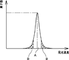
- FIG. 10 is a diagram showing the emission wavelength distribution of the light emitting elements on the holding means obtained by the wavelength measurement section of the transfer system and the result of grouping by the transfer position determination section;
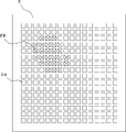
- FIG. 10 is a diagram showing light-emitting elements on the holding means reflecting grouping by the transfer position determining unit;
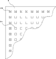
- FIG. 10 is a diagram showing an example of a transferred substrate on which a light emitting element is transferred reflecting transfer position information determined by a transfer position determination unit; It is a figure explaining the transcription
- FIG. 10 is a diagram showing a result of grouping by a transfer position determination unit in another embodiment;
- a transfer system 1 according to one embodiment of the present invention will be described with reference to FIG.
- the transfer system 1 of this embodiment has a transfer section 10 , a wavelength measurement section 20 , and a transfer position determination section 30 . transcribed to In addition, the arrangement (layout) of the light emitting elements 2 on the holding means 3 is not directly reflected on the layout on the substrate 4 to be transferred. is measured, and the transfer position determination unit 30 determines the transfer position of each light emitting element 2 on the substrate 4 to be transferred based on the obtained information of the emission wavelength of each light emitting element 2 . Based on this transfer position information, the transfer section 10 transfers each light emitting element 2 to the transferred substrate 4 .
- the light emitting element 2 is a micro LED chip
- the transfer substrate 4 is a circuit board for display. Red, green, and blue light-emitting elements 2 are arranged on the transferred substrate 4, and the number of arranged is 1920 ⁇ for each color when the transferred substrate 4 is a circuit board for FHD (Full High Definition) panel. 1,080, and 3,840 x 2,160 for a circuit board for a 4K panel.
- FHD Full Definition
- the holding means 3 may be a growth substrate that serves as a base for epitaxial growth of the LED chip, or may be an intermediate substrate in the case of completing the transfer of the light emitting element 2 from the growth substrate to the circuit board through multiple transfers. Also good.
- the shape of the holding means 3 may be a wafer shape or a square plate shape.
- a known form capable of causing laser ablation is applied to the form of holding the light emitting element 2 by the holding means 3 .
- the horizontal directions that are perpendicular to each other are called the X-axis direction and the Y-axis direction, respectively, and the vertical direction is called the Z-axis direction.
- the transfer unit 10 transfers the light emitting element 2 held by the holding means 3 to the transferred substrate 4 by utilizing laser lift-off.
- a hand 14 and a placement section 15 are provided.
- the back surface of the holding means 3 is suction-held by the suction hand 14 so that the surface (referred to as the surface) on which the light emitting element 2 is held is horizontal and downward.
- the rear surface of the substrate 4 to be transferred is sucked and held by the mounting portion 15 so that the surface (referred to as the surface) onto which the light emitting elements 2 are transferred is horizontal and faces upward.
- the holding means 3 and the transferred substrate 4 face each other vertically, and the holding means 3 is positioned on the upper side.
- the laser light source 11 is a device that emits a single laser beam L1, and in this embodiment emits laser beams such as a YAG laser, a visible light laser, and an ultraviolet laser.
- the galvanomirror 12 has two mirrors, and by controlling the positions and angles of these mirrors, incident light rays can be emitted in arbitrary directions.
- a pulsed laser beam L1 emitted from the laser light source 11 passes through the galvanomirror 12 and the F ⁇ lens 13 and irradiates the holding means 3 held by the suction hand 14 . Then, the laser beam L1 irradiated onto the holding means 3 passes through the holding means 3 and reaches the interface between the holding means 3 and the light emitting element 2, causing laser ablation at this interface. By this laser ablation, the light-emitting element 2 is energized and separated from the holding means 3, and transferred to the transfer-receiving substrate 4 immediately below. In this description, separating the light-emitting element 2 from the holding means 3 by laser ablation is called laser lift-off.
- the optical path of the laser beam L1 is controlled by the galvanomirror 12 so that it can irradiate an arbitrary position on the holding means 3.
- the galvanomirror 12 By having the galvanomirror 12 in this way, the light-emitting element 2 at any position held by the holding means 3 can be laser lifted off.
- the mounting section 15 is movable in the X-axis direction and the Y-axis direction by the moving stage 16, and relatively moves the transferred substrate 4 in the X-axis direction and the Y-axis direction with respect to the holding means 3.
- the position control of the transferred substrate 4 by the moving stage 16 and the irradiation position control of the laser light L1 by the galvanomirror 12 the light emitting element 2 held by the holding means 3 at an arbitrary position can be moved to the transferred substrate. It is possible to transfer to any position on 4 .
- the wavelength measurement unit 20 is an embodiment of the light emission characteristic measurement unit referred to in this description.
- photoluminescence is used to measure the light emission wavelength, which is a kind of light emission characteristic of each light emitting element 2 on the holding means 3. It measures, and includes a laser light source 21 , a wavelength measuring device 22 , and a mounting section 23 .
- the back surface of the holding unit 3 is sucked and held by the mounting unit 23 so that the surface (front surface) where the light emitting element 2 is held is horizontal and faces upward.
- the laser light source 21 is a device that emits a single laser beam L2, and in this embodiment emits laser beams such as a YAG laser, a visible light laser, and an ultraviolet laser.
- the above laser light is one embodiment of the active energy ray in the present invention, and in addition to laser light, the active energy ray includes electromagnetic waves, particle beams, quantum beams, elementary particle beams, and the like.
- the wavelength measuring device 22 measures the wavelength of light incident on itself, and a known optical wavelength meter is applied.
- the mounting section 23 can be moved in the X-axis direction and the Y-axis direction by a moving stage 24, and the holding means 3 can be moved relative to the laser light source 21 and the wavelength measuring device 22 in the X-axis direction and the Y-axis direction. move.
- the holding means 3 By controlling the position of the holding means 3 by the moving stage 24, it is possible to measure the emission wavelength of the light emitting element 2 held by the holding means 3 at an arbitrary position.
- This wavelength measuring unit 20 measures the emission wavelengths of all the light emitting elements 2 held by the holding means 3 .
- the transfer position determination unit 30 is also referred to as a transfer position determination device in this description, and in this embodiment is a computer that controls the operations of the transfer unit 10 and the wavelength measurement unit 20 . has a program for creating transfer position information (transfer position information) of each light emitting element 2 on the transferred substrate 4 based on the information of the emission wavelength of each light emitting element 2 . Based on this transfer position information, the transfer section 10 transfers a predetermined light emitting element 2 on the holding means 3 to a predetermined position on the transfer substrate 4 .
- FIG. 2 is a graph showing the distribution of emission wavelengths of the light emitting elements 2 on the holding means 3 obtained by the wavelength measuring section 20.
- the horizontal axis is the emission wavelength
- the vertical axis is the number of light emitting elements 2 that emit light at each emission wavelength (the number of elements).
- this distribution is classified into two groups: Group A in a predetermined wavelength range including emission wavelengths having the mode value (mode value), and Group B, which is a group outside Group A.
- the light-emitting elements 2 with emission wavelengths belonging to group A are called mode elements 2A
- the light-emitting elements 2 with emission wavelengths belonging to group B are called non-mode elements 2B.
- the boundary value between group A and group B is set so that the number of mode elements 2A is smaller than the number of non-mode elements 2B.
- FIG. 3 is a diagram showing an example of the arrangement of the light emitting elements 2 on the holding means 3 reflecting the above grouping, and the non-mode elements 2B are hatched.
- the transfer position determination unit 30 selects the non-mode element 2B based on the information on the light emission characteristics of each of the light emitting elements 2 on the holding means 3 within a range that does not cause unevenness in the display, which is the final product. Transfer position information is created so as to be arranged on the transferred substrate 4 .
- FIG. 4 is a diagram showing an example of the transferred substrate 4 on which the light emitting element 2 has been transferred with the transfer position information determined by the transfer position determination unit 30 reflected.
- transfer position information is created by the transfer position determination unit 30 so that the non-mode element 2B is preferentially used and transferred to the outer peripheral portion of the transfer substrate 4, and the holding means 3
- the light emitting element 2 is transferred from the substrate 4 to the substrate 4 to be transferred.
- the non-mode element 2B can also be used to form a display by effectively utilizing the outer peripheral portion where unevenness is less noticeable, and a display that does not generate unevenness while maintaining a high yield of light emitting elements. can be formed.
- the emission wavelength which is the boundary between group A and group B in FIG. 2, in consideration of the emission wavelength distribution.
- the emission wavelength range of 600 nm to 780 nm for red LEDs, 505 nm to 530 nm for green LEDs, and 470 to 485 nm for blue LEDs is group A
- the emission wavelength range outside the range is group B.
- the transfer position determination unit 30 calculates the arrangement of the mode element 2A and the non-mode element 2B based on this condition. Further, such a range of emission wavelengths may be automatically determined by the transfer position determining section 30 .
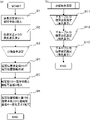
- FIG. 5 is a flow chart explaining a transfer method using the transfer system of the above embodiment.
- FIG. 5(a) is a flowchart showing a series of processes related to transfer of the light emitting element 2 from the holding means 3 to the transferred substrate 4.
- FIG. 5(a) is a flowchart showing a series of processes related to transfer of the light emitting element 2 from the holding means 3 to the transferred substrate 4.
- the holding means 3 is put into the wavelength measuring section 20 (step S1), and the emission wavelength of each light emitting element 2 on the holding means 3 is measured by the wavelength measuring section 20 (step S2).
- the step of measuring the emission characteristics such as the emission wavelength of each light emitting element 2 held by the holding means 3 as in step S2 is referred to as the emission characteristics measurement step.
- each light emitting element 2 is classified based on the information on the emission wavelength of each light emitting element 2 obtained in the above light emitting characteristic measurement step, and the transfer position on the transferred substrate 4 is determined. Specifically, a classification condition is set (step S3), and the transfer position determination unit 30 is operated so that the light emitting element 2 identified as the non-mode element 2B by this classification is arranged on the outer peripheral portion of the substrate 4 to be transferred. Transfer position information of each light emitting element 2 to the transferred substrate 4 is created (step S4). In this description, the step of creating transfer position information of each light emitting element 2 onto the transferred substrate 4 as in step S4 is called a transfer position determination step.
- step S3 Details of the classification condition setting in step S3 are shown in FIG. 5(b).
- a boundary value for distinguishing between group A and group B in FIG. 2 is set for each color light-emitting element 2 .
- Boundary values for grouping (classifying) the light emitting elements 2 of each color are set (steps S11 and S12). , step S13).
- the setting of this boundary value may be performed manually, or may be performed automatically by the transfer position determining section 30, for example.
- the step of setting the classification condition is included in the series of processes, but this setting may be performed in advance at a stage prior to step S1.
- step S4 After the transfer position information is created in step S4, the holding means 3 is taken out from the wavelength measuring section 20 and put into the transfer section 10. FIG. Also, the transferred substrate 4 is also put into the transfer section 10 (step S5). Finally, according to the transfer position information, the transfer unit 10 transfers the mode element 2A and the non-mode element 2B from the holding means 3 to the transferred substrate 4 (step S6).
- the process of transferring the light emitting element 2 from the holding means 3 to the substrate 4 to be transferred based on the transfer position information obtained by the transfer position determination process like this step S6 is called a transfer process.
- the transferred substrate 4 with the light emitting elements 2 transferred thereon so that the unevenness is not visually recognized is completed.
- a post-process such as mounting may be performed, and an unevenness inspection may be performed in order to detect any defects.
- FIG. 6 is a diagram showing the result of grouping by the transfer position determination unit 30 in another embodiment.
- the grouping for the distribution of emission wavelengths of the light emitting elements 2 does not necessarily have to be two groups.
- the light-emitting elements 2 on the holding means 3 are group D, which is a group of ranges including the most frequent emission wavelength, and group E, which is a group of emission wavelength ranges adjacent to the outside of group D, and group E. are classified into three groups, Group F, which is the group of emission wavelength ranges adjacent to the outside of the .
- the transfer position determination unit 30 creates transfer position information so that only non-mode elements belonging to E are transferred. In this manner, the transfer position determination unit 30 may create information on not only the transfer position on the transfer substrate 4 but also whether or not the transfer is possible.
- the yield is slightly lowered, the number of non-mode elements can be relatively reduced. can be easily formed.
- the transfer system, transfer position determination device, and transfer method of the present invention are not limited to the forms described above, and may be of other forms within the scope of the present invention.
- the light emission characteristics of the light emitting elements 2 measured by the light emission characteristic measuring unit are not limited to the light emission wavelength, and may be the light emission luminance of each light emitting element 2, for example.
- the transfer method of the light emitting element 2 by the transfer unit 10 is not limited to laser lift-off, and other known methods may be used.
- the light emitting element 2 may be transferred by so-called bonding using thermocompression bonding, ultrasonic waves, or the like.
- transfer system 2 light emitting element 2A mode element 2B non-mode element 3 holding means 4 substrate to be transferred 10 transfer unit 11 laser light source 12 galvanomirror 13 F ⁇ lens 14 suction hand 15 placement unit 16 movement stage 20 wavelength measurement unit 21 laser light source 22 Wavelength measuring device 23 Mounting unit 24 Moving stage 30 Transfer position determining unit A Group B Group C Group D Group E Group L1 Laser light L2 Laser light L3 Emission light W Distance
Landscapes
- Physics & Mathematics (AREA)
- General Physics & Mathematics (AREA)
- Engineering & Computer Science (AREA)
- Theoretical Computer Science (AREA)
- Analytical Chemistry (AREA)
- Immunology (AREA)
- Life Sciences & Earth Sciences (AREA)
- Chemical & Material Sciences (AREA)
- Spectroscopy & Molecular Physics (AREA)
- Biochemistry (AREA)
- General Health & Medical Sciences (AREA)
- Health & Medical Sciences (AREA)
- Pathology (AREA)
- Led Device Packages (AREA)
- Led Devices (AREA)
- Die Bonding (AREA)
- Container, Conveyance, Adherence, Positioning, Of Wafer (AREA)
- Devices For Indicating Variable Information By Combining Individual Elements (AREA)
- Testing Of Optical Devices Or Fibers (AREA)
Abstract
Description
2 発光素子
2A モード素子
2B 非モード素子
3 保持手段
4 被転写基板
10 転写部
11 レーザー光源
12 ガルバノミラー
13 Fθレンズ
14 吸着ハンド
15 載置部
16 移動ステージ
20 波長測定部
21 レーザー光源
22 波長測定器
23 載置部
24 移動ステージ
30 転写位置決定部
A グループ
B グループ
C グループ
D グループ
E グループ
L1 レーザー光
L2 レーザー光
L3 放出光
W 距離
Claims (7)
- 保持手段によって保持された複数の発光素子を被転写基板へ転写させる転写システムであり、
前記保持手段に保持された状態の各々の前記発光素子の発光特性を測定する発光特性測定部と、
前記発光特性測定部によって得られた前記保持手段上の各々の前記発光素子の発光特性の情報をもとに、各々の前記発光素子に対し転写可否および/または前記被転写基板上の転写位置情報を作成する転写位置決定部と、
前記転写位置決定部によって作成された転写位置情報をもとに、前記保持手段から前記被転写基板へ前記発光素子を転写させる転写部と、
を備えることを特徴とする、転写システム。 - 前記発光特性測定部は、前記保持手段に保持された状態の各々の前記発光素子に活性エネルギー線を照射することにより前記発光素子から発光される蛍光や燐光の波長を測定する波長測定部であることを特徴とする、請求項1に記載の転写システム。
- 前記転写部は、レーザーリフトオフにより前記保持手段上の各々の前記発光素子を前記被転写基板へ転写させることを特徴とする、請求項1もしくは2に記載の転写システム。
- 前記転写部は、熱圧着により前記保持手段上の各々の前記発光素子を前記被転写基板へ転写させることを特徴とする、請求項1もしくは2に記載の転写システム。
- 前記転写部は、超音波により前記保持手段上の各々の前記発光素子を前記被転写基板へ転写させることを特徴とする、請求項1もしくは2に記載の転写システム。
- 保持手段によって保持された複数の発光素子を被転写基板へ転写させるにあたり、前記保持手段上の各々の前記発光素子の発光特性の情報をもとに、各々の前記発光素子に対し転写可否および/または前記被転写基板上の転写位置情報を作成することを特徴とする、転写位置決定装置。
- 保持手段によって保持された複数の発光素子を被転写基板へ転写させる転写方法であり、
前記保持手段に保持された状態の各々の前記発光素子の発光特性を測定する発光特性測定工程と、
前記発光特性測定工程によって得られた前記保持手段上の各々の前記発光素子の発光特性の情報をもとに、各々の前記発光素子に対し転写可否および/または前記被転写基板上の転写位置情報を作成する転写位置決定工程と、
前記転写位置決定工程によって作成された転写位置情報をもとに、前記保持手段から前記被転写基板へ前記発光素子を転写させる転写工程と、
を備えることを特徴とする、転写方法。
Priority Applications (2)
| Application Number | Priority Date | Filing Date | Title |
|---|---|---|---|
| CN202180094785.1A CN116888749A (zh) | 2021-03-05 | 2021-12-23 | 转印系统、转印位置决定装置以及转印方法 |
| KR1020237029859A KR102851516B1 (ko) | 2021-03-05 | 2021-12-23 | 전사 시스템, 전사 위치 결정 장치, 및 전사 방법 |
Applications Claiming Priority (2)
| Application Number | Priority Date | Filing Date | Title |
|---|---|---|---|
| JP2021035380A JP7524108B2 (ja) | 2021-03-05 | 2021-03-05 | 転写システム、転写位置決定装置、および転写方法 |
| JP2021-035380 | 2021-03-05 |
Publications (1)
| Publication Number | Publication Date |
|---|---|
| WO2022185686A1 true WO2022185686A1 (ja) | 2022-09-09 |
Family
ID=83153939
Family Applications (1)
| Application Number | Title | Priority Date | Filing Date |
|---|---|---|---|
| PCT/JP2021/047870 Ceased WO2022185686A1 (ja) | 2021-03-05 | 2021-12-23 | 転写システム、転写位置決定装置、および転写方法 |
Country Status (4)
| Country | Link |
|---|---|
| JP (1) | JP7524108B2 (ja) |
| KR (1) | KR102851516B1 (ja) |
| CN (1) | CN116888749A (ja) |
| WO (1) | WO2022185686A1 (ja) |
Families Citing this family (1)
| Publication number | Priority date | Publication date | Assignee | Title |
|---|---|---|---|---|
| KR102841310B1 (ko) * | 2023-11-23 | 2025-08-04 | 엘지전자 주식회사 | 발광 소자를 이용한 디스플레이 장치 및 그 제조 방법 |
Citations (3)
| Publication number | Priority date | Publication date | Assignee | Title |
|---|---|---|---|---|
| JP2010087064A (ja) * | 2008-09-30 | 2010-04-15 | Sony Corp | 表示装置の製造方法 |
| US20130163228A1 (en) * | 2011-12-21 | 2013-06-27 | Samsung Electronics Co., Ltd. | Light source module and backlight unit |
| JP2015031894A (ja) * | 2013-08-06 | 2015-02-16 | 三菱電機株式会社 | 映像表示装置およびその製造方法 |
Family Cites Families (4)
| Publication number | Priority date | Publication date | Assignee | Title |
|---|---|---|---|---|
| JP4431925B2 (ja) | 2000-11-30 | 2010-03-17 | 信越半導体株式会社 | 発光素子の製造方法 |
| US8202741B2 (en) * | 2009-03-04 | 2012-06-19 | Koninklijke Philips Electronics N.V. | Method of bonding a semiconductor device using a compliant bonding structure |
| JP2018060993A (ja) * | 2016-09-29 | 2018-04-12 | 東レエンジニアリング株式会社 | 転写方法、実装方法、転写装置、及び実装装置 |
| KR102652723B1 (ko) * | 2018-11-20 | 2024-04-01 | 삼성전자주식회사 | 마이크로 led 전사 장치 및 이를 이용한 마이크로 led 전사 방법 |
-
2021
- 2021-03-05 JP JP2021035380A patent/JP7524108B2/ja active Active
- 2021-12-23 WO PCT/JP2021/047870 patent/WO2022185686A1/ja not_active Ceased
- 2021-12-23 KR KR1020237029859A patent/KR102851516B1/ko active Active
- 2021-12-23 CN CN202180094785.1A patent/CN116888749A/zh active Pending
Patent Citations (3)
| Publication number | Priority date | Publication date | Assignee | Title |
|---|---|---|---|---|
| JP2010087064A (ja) * | 2008-09-30 | 2010-04-15 | Sony Corp | 表示装置の製造方法 |
| US20130163228A1 (en) * | 2011-12-21 | 2013-06-27 | Samsung Electronics Co., Ltd. | Light source module and backlight unit |
| JP2015031894A (ja) * | 2013-08-06 | 2015-02-16 | 三菱電機株式会社 | 映像表示装置およびその製造方法 |
Also Published As
| Publication number | Publication date |
|---|---|
| JP7524108B2 (ja) | 2024-07-29 |
| CN116888749A (zh) | 2023-10-13 |
| KR20230150975A (ko) | 2023-10-31 |
| JP2022135521A (ja) | 2022-09-15 |
| KR102851516B1 (ko) | 2025-08-27 |
Similar Documents
| Publication | Publication Date | Title |
|---|---|---|
| TWI735695B (zh) | 用於在基板間轉移電子元件的方法及設備 | |
| JP6983811B2 (ja) | 発光デバイスアセンブリ上の選択的ダイ修理 | |
| KR102888426B1 (ko) | 레이저 전사 장치 및 이를 이용한 전사 방법 | |
| JP2019530201A (ja) | マイクロデバイスのマスクレス並列ピックアンドプレース移載 | |
| JP7638650B2 (ja) | チップ転写方法及びチップ転写装置 | |
| US10580825B2 (en) | Method of manufacturing display device Including Photoluminescence measurement | |
| JP6985031B2 (ja) | Ledディスプレーパネルの製造方法 | |
| TWI795618B (zh) | 檢查裝置及檢查方法 | |
| KR102652723B1 (ko) | 마이크로 led 전사 장치 및 이를 이용한 마이크로 led 전사 방법 | |
| JP6911003B2 (ja) | 素子アレイの製造方法と特定素子の除去方法 | |
| JP6542971B1 (ja) | 検査装置及び検査方法 | |
| WO2022221628A1 (en) | System and method for probing and sorting led chips | |
| WO2022185686A1 (ja) | 転写システム、転写位置決定装置、および転写方法 | |
| TWI896626B (zh) | 安裝方法、安裝裝置及轉印裝置 | |
| TWM596869U (zh) | 用於大面積顯微光致螢光掃描與側繪量測的系統 | |
| JP2022115687A (ja) | 転写装置 | |
| US20230106834A1 (en) | Method of manufacturing optoelectronic products and apparatus thereof | |
| JP2020095223A (ja) | 素子アレイの製造装置と特定素子の除去装置 | |
| US20260040741A1 (en) | Method and apparatus for transferring electronic devices | |
| JP2024179880A (ja) | 転写方法 | |
| JP2025004642A (ja) | 転写方法 | |
| Flemish et al. | Development and industrialization of InGaN/GaN LEDs on patterned sapphire substrates for low cost emitter architecture | |
| JP2017168469A (ja) | 発光装置の製造方法、発光装置、および発光装置の製造装置 | |
| JP2022178157A (ja) | 表示装置の製造方法および保持基板 | |
| CN102128816A (zh) | 发光元件的缺陷检测方法及系统 |
Legal Events
| Date | Code | Title | Description |
|---|---|---|---|
| 121 | Ep: the epo has been informed by wipo that ep was designated in this application |
Ref document number: 21929242 Country of ref document: EP Kind code of ref document: A1 |
|
| WWE | Wipo information: entry into national phase |
Ref document number: 202180094785.1 Country of ref document: CN |
|
| ENP | Entry into the national phase |
Ref document number: 20237029859 Country of ref document: KR Kind code of ref document: A |
|
| NENP | Non-entry into the national phase |
Ref country code: DE |
|
| 122 | Ep: pct application non-entry in european phase |
Ref document number: 21929242 Country of ref document: EP Kind code of ref document: A1 |