WO2022181196A1 - Puce de détection, procédé de fabrication de puce de détection, kit de détection, procédé de mesure et dispositif de mesure - Google Patents
Puce de détection, procédé de fabrication de puce de détection, kit de détection, procédé de mesure et dispositif de mesure Download PDFInfo
- Publication number
- WO2022181196A1 WO2022181196A1 PCT/JP2022/003209 JP2022003209W WO2022181196A1 WO 2022181196 A1 WO2022181196 A1 WO 2022181196A1 JP 2022003209 W JP2022003209 W JP 2022003209W WO 2022181196 A1 WO2022181196 A1 WO 2022181196A1
- Authority
- WO
- WIPO (PCT)
- Prior art keywords
- plasmon
- chip
- generation region
- bound
- light
- Prior art date
Links
- 238000004519 manufacturing process Methods 0.000 title claims description 27
- 238000000034 method Methods 0.000 title claims description 16
- 238000005259 measurement Methods 0.000 title claims description 5
- 238000000691 measurement method Methods 0.000 title description 3
- 239000000758 substrate Substances 0.000 claims abstract description 43
- 239000013076 target substance Substances 0.000 claims abstract description 26
- 230000000737 periodic effect Effects 0.000 claims abstract description 19
- 150000001875 compounds Chemical class 0.000 claims description 80
- YBJHBAHKTGYVGT-ZKWXMUAHSA-N (+)-Biotin Chemical compound N1C(=O)N[C@@H]2[C@H](CCCCC(=O)O)SC[C@@H]21 YBJHBAHKTGYVGT-ZKWXMUAHSA-N 0.000 claims description 28
- 230000005684 electric field Effects 0.000 claims description 28
- 229960002685 biotin Drugs 0.000 claims description 25
- 239000011616 biotin Substances 0.000 claims description 25
- 230000001678 irradiating effect Effects 0.000 claims description 23
- WYTZZXDRDKSJID-UHFFFAOYSA-N (3-aminopropyl)triethoxysilane Chemical compound CCO[Si](OCC)(OCC)CCCN WYTZZXDRDKSJID-UHFFFAOYSA-N 0.000 claims description 22
- 239000000126 substance Substances 0.000 claims description 18
- 235000020958 biotin Nutrition 0.000 claims description 15
- PEEHTFAAVSWFBL-UHFFFAOYSA-N Maleimide Chemical compound O=C1NC(=O)C=C1 PEEHTFAAVSWFBL-UHFFFAOYSA-N 0.000 claims description 3
- 230000035945 sensitivity Effects 0.000 abstract description 16
- 238000001514 detection method Methods 0.000 abstract description 8
- 239000010410 layer Substances 0.000 description 43
- BTFQKIATRPGRBS-UHFFFAOYSA-N o-tolualdehyde Chemical compound CC1=CC=CC=C1C=O BTFQKIATRPGRBS-UHFFFAOYSA-N 0.000 description 34
- 230000001737 promoting effect Effects 0.000 description 25
- -1 aryl azide Chemical class 0.000 description 22
- HUMNYLRZRPPJDN-UHFFFAOYSA-N benzaldehyde Chemical compound O=CC1=CC=CC=C1 HUMNYLRZRPPJDN-UHFFFAOYSA-N 0.000 description 22
- 229910052751 metal Inorganic materials 0.000 description 21
- 239000002184 metal Substances 0.000 description 21
- 230000000052 comparative effect Effects 0.000 description 19
- 238000010791 quenching Methods 0.000 description 19
- 230000000171 quenching effect Effects 0.000 description 19
- 238000006243 chemical reaction Methods 0.000 description 16
- 230000003287 optical effect Effects 0.000 description 16
- 244000309464 bull Species 0.000 description 13
- 230000000694 effects Effects 0.000 description 13
- 238000010586 diagram Methods 0.000 description 12
- JKHVDAUOODACDU-UHFFFAOYSA-N (2,5-dioxopyrrolidin-1-yl) 3-(2,5-dioxopyrrol-1-yl)propanoate Chemical compound O=C1CCC(=O)N1OC(=O)CCN1C(=O)C=CC1=O JKHVDAUOODACDU-UHFFFAOYSA-N 0.000 description 11
- ZMXDDKWLCZADIW-UHFFFAOYSA-N N,N-Dimethylformamide Chemical compound CN(C)C=O ZMXDDKWLCZADIW-UHFFFAOYSA-N 0.000 description 11
- QNGNSVIICDLXHT-UHFFFAOYSA-N para-ethylbenzaldehyde Natural products CCC1=CC=C(C=O)C=C1 QNGNSVIICDLXHT-UHFFFAOYSA-N 0.000 description 11
- 239000012790 adhesive layer Substances 0.000 description 10
- 239000000427 antigen Substances 0.000 description 10
- 102000036639 antigens Human genes 0.000 description 10
- 108091007433 antigens Proteins 0.000 description 10
- ZMANZCXQSJIPKH-UHFFFAOYSA-N Triethylamine Chemical compound CCN(CC)CC ZMANZCXQSJIPKH-UHFFFAOYSA-N 0.000 description 9
- CIVGYTYIDWRBQU-UFLZEWODSA-N 5-[(3as,4s,6ar)-2-oxo-1,3,3a,4,6,6a-hexahydrothieno[3,4-d]imidazol-4-yl]pentanoic acid;pyrrole-2,5-dione Chemical compound O=C1NC(=O)C=C1.N1C(=O)N[C@@H]2[C@H](CCCCC(=O)O)SC[C@@H]21 CIVGYTYIDWRBQU-UFLZEWODSA-N 0.000 description 7
- 230000001133 acceleration Effects 0.000 description 7
- VYPSYNLAJGMNEJ-UHFFFAOYSA-N Silicium dioxide Chemical compound O=[Si]=O VYPSYNLAJGMNEJ-UHFFFAOYSA-N 0.000 description 6
- 239000010408 film Substances 0.000 description 6
- 230000002093 peripheral effect Effects 0.000 description 6
- 239000000243 solution Substances 0.000 description 6
- 230000001629 suppression Effects 0.000 description 6
- 229910004298 SiO 2 Inorganic materials 0.000 description 5
- 229910052736 halogen Inorganic materials 0.000 description 5
- 150000002367 halogens Chemical class 0.000 description 5
- 239000000463 material Substances 0.000 description 5
- QSHDDOUJBYECFT-UHFFFAOYSA-N mercury Chemical compound [Hg] QSHDDOUJBYECFT-UHFFFAOYSA-N 0.000 description 5
- 229910052753 mercury Inorganic materials 0.000 description 5
- 239000008363 phosphate buffer Substances 0.000 description 5
- 238000001179 sorption measurement Methods 0.000 description 5
- 238000002198 surface plasmon resonance spectroscopy Methods 0.000 description 5
- 238000005406 washing Methods 0.000 description 5
- 238000002474 experimental method Methods 0.000 description 4
- 238000002073 fluorescence micrograph Methods 0.000 description 4
- 102000004169 proteins and genes Human genes 0.000 description 4
- 108090000623 proteins and genes Proteins 0.000 description 4
- 239000010936 titanium Substances 0.000 description 4
- LMDZBCPBFSXMTL-UHFFFAOYSA-N 1-Ethyl-3-(3-dimethylaminopropyl)carbodiimide Substances CCN=C=NCCCN(C)C LMDZBCPBFSXMTL-UHFFFAOYSA-N 0.000 description 3
- 108090001008 Avidin Proteins 0.000 description 3
- 238000010521 absorption reaction Methods 0.000 description 3
- 230000015572 biosynthetic process Effects 0.000 description 3
- 230000002708 enhancing effect Effects 0.000 description 3
- 230000005284 excitation Effects 0.000 description 3
- 125000005439 maleimidyl group Chemical group C1(C=CC(N1*)=O)=O 0.000 description 3
- 239000011241 protective layer Substances 0.000 description 3
- 239000000377 silicon dioxide Substances 0.000 description 3
- 238000004544 sputter deposition Methods 0.000 description 3
- 229920001213 Polysorbate 20 Polymers 0.000 description 2
- BLRPTPMANUNPDV-UHFFFAOYSA-N Silane Chemical compound [SiH4] BLRPTPMANUNPDV-UHFFFAOYSA-N 0.000 description 2
- BQCADISMDOOEFD-UHFFFAOYSA-N Silver Chemical compound [Ag] BQCADISMDOOEFD-UHFFFAOYSA-N 0.000 description 2
- 108010090804 Streptavidin Proteins 0.000 description 2
- RTAQQCXQSZGOHL-UHFFFAOYSA-N Titanium Chemical compound [Ti] RTAQQCXQSZGOHL-UHFFFAOYSA-N 0.000 description 2
- 125000003277 amino group Chemical group 0.000 description 2
- 239000011324 bead Substances 0.000 description 2
- 238000004166 bioassay Methods 0.000 description 2
- 239000003153 chemical reaction reagent Substances 0.000 description 2
- 239000011651 chromium Substances 0.000 description 2
- 239000012141 concentrate Substances 0.000 description 2
- 201000010099 disease Diseases 0.000 description 2
- 208000037265 diseases, disorders, signs and symptoms Diseases 0.000 description 2
- 239000010931 gold Substances 0.000 description 2
- 230000006872 improvement Effects 0.000 description 2
- 230000003993 interaction Effects 0.000 description 2
- 229920003229 poly(methyl methacrylate) Polymers 0.000 description 2
- 239000004926 polymethyl methacrylate Substances 0.000 description 2
- 239000000256 polyoxyethylene sorbitan monolaurate Substances 0.000 description 2
- 235000010486 polyoxyethylene sorbitan monolaurate Nutrition 0.000 description 2
- 238000011896 sensitive detection Methods 0.000 description 2
- 229910000077 silane Inorganic materials 0.000 description 2
- 229910052709 silver Inorganic materials 0.000 description 2
- 239000004332 silver Substances 0.000 description 2
- 239000004094 surface-active agent Substances 0.000 description 2
- 230000002195 synergetic effect Effects 0.000 description 2
- 239000010409 thin film Substances 0.000 description 2
- 229910052719 titanium Inorganic materials 0.000 description 2
- CVOFKRWYWCSDMA-UHFFFAOYSA-N 2-chloro-n-(2,6-diethylphenyl)-n-(methoxymethyl)acetamide;2,6-dinitro-n,n-dipropyl-4-(trifluoromethyl)aniline Chemical compound CCC1=CC=CC(CC)=C1N(COC)C(=O)CCl.CCCN(CCC)C1=C([N+]([O-])=O)C=C(C(F)(F)F)C=C1[N+]([O-])=O CVOFKRWYWCSDMA-UHFFFAOYSA-N 0.000 description 1
- FPQQSJJWHUJYPU-UHFFFAOYSA-N 3-(dimethylamino)propyliminomethylidene-ethylazanium;chloride Chemical compound Cl.CCN=C=NCCCN(C)C FPQQSJJWHUJYPU-UHFFFAOYSA-N 0.000 description 1
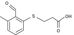
- UVMPVNABHZZSMW-UHFFFAOYSA-N CC1=CC=CC(SCCC(O)=O)=C1C=O Chemical compound CC1=CC=CC(SCCC(O)=O)=C1C=O UVMPVNABHZZSMW-UHFFFAOYSA-N 0.000 description 1
- VYZAMTAEIAYCRO-UHFFFAOYSA-N Chromium Chemical compound [Cr] VYZAMTAEIAYCRO-UHFFFAOYSA-N 0.000 description 1
- 208000035473 Communicable disease Diseases 0.000 description 1
- 241001590997 Moolgarda engeli Species 0.000 description 1
- 240000007594 Oryza sativa Species 0.000 description 1
- 235000007164 Oryza sativa Nutrition 0.000 description 1
- 229910052782 aluminium Inorganic materials 0.000 description 1
- XAGFODPZIPBFFR-UHFFFAOYSA-N aluminium Chemical compound [Al] XAGFODPZIPBFFR-UHFFFAOYSA-N 0.000 description 1
- 238000000089 atomic force micrograph Methods 0.000 description 1
- 230000002238 attenuated effect Effects 0.000 description 1
- 229910052804 chromium Inorganic materials 0.000 description 1
- 238000010276 construction Methods 0.000 description 1
- 230000008878 coupling Effects 0.000 description 1
- 238000010168 coupling process Methods 0.000 description 1
- 238000005859 coupling reaction Methods 0.000 description 1
- 238000004132 cross linking Methods 0.000 description 1
- 238000006297 dehydration reaction Methods 0.000 description 1
- 238000011161 development Methods 0.000 description 1
- 229940079593 drug Drugs 0.000 description 1
- 239000003814 drug Substances 0.000 description 1
- 238000011156 evaluation Methods 0.000 description 1
- 238000002795 fluorescence method Methods 0.000 description 1
- 239000011521 glass Substances 0.000 description 1
- PCHJSUWPFVWCPO-UHFFFAOYSA-N gold Chemical compound [Au] PCHJSUWPFVWCPO-UHFFFAOYSA-N 0.000 description 1
- 229910052737 gold Inorganic materials 0.000 description 1
- 238000005286 illumination Methods 0.000 description 1
- 238000003384 imaging method Methods 0.000 description 1
- 238000003018 immunoassay Methods 0.000 description 1
- 238000001746 injection moulding Methods 0.000 description 1
- 238000002372 labelling Methods 0.000 description 1
- 239000004005 microsphere Substances 0.000 description 1
- 239000002052 molecular layer Substances 0.000 description 1
- 238000000465 moulding Methods 0.000 description 1
- 239000002105 nanoparticle Substances 0.000 description 1
- 239000008055 phosphate buffer solution Substances 0.000 description 1
- 230000002186 photoactivation Effects 0.000 description 1
- 238000006552 photochemical reaction Methods 0.000 description 1
- 229920003023 plastic Polymers 0.000 description 1
- 239000004033 plastic Substances 0.000 description 1
- 238000002360 preparation method Methods 0.000 description 1
- 230000008569 process Effects 0.000 description 1
- 230000001902 propagating effect Effects 0.000 description 1
- 238000011158 quantitative evaluation Methods 0.000 description 1
- 239000000376 reactant Substances 0.000 description 1
- 238000011160 research Methods 0.000 description 1
- 235000009566 rice Nutrition 0.000 description 1
- 235000012239 silicon dioxide Nutrition 0.000 description 1
- 238000012546 transfer Methods 0.000 description 1
Images


Classifications
-
- G—PHYSICS
- G01—MEASURING; TESTING
- G01N—INVESTIGATING OR ANALYSING MATERIALS BY DETERMINING THEIR CHEMICAL OR PHYSICAL PROPERTIES
- G01N21/00—Investigating or analysing materials by the use of optical means, i.e. using sub-millimetre waves, infrared, visible or ultraviolet light
- G01N21/17—Systems in which incident light is modified in accordance with the properties of the material investigated
- G01N21/55—Specular reflectivity
- G01N21/552—Attenuated total reflection
-
- G—PHYSICS
- G01—MEASURING; TESTING
- G01N—INVESTIGATING OR ANALYSING MATERIALS BY DETERMINING THEIR CHEMICAL OR PHYSICAL PROPERTIES
- G01N21/00—Investigating or analysing materials by the use of optical means, i.e. using sub-millimetre waves, infrared, visible or ultraviolet light
- G01N21/62—Systems in which the material investigated is excited whereby it emits light or causes a change in wavelength of the incident light
- G01N21/63—Systems in which the material investigated is excited whereby it emits light or causes a change in wavelength of the incident light optically excited
- G01N21/64—Fluorescence; Phosphorescence
Definitions
- the present invention relates to a sensing chip that detects a target substance using the interaction of surface plasmon resonance, a method for manufacturing a sensing chip, a sensing kit, a measuring method, and a measuring device.
- Non-Patent Document 1 discloses a chip with a bull's eye structure, which is composed of concentric circles and whose cross section passing through the center has a periodic structure. Specifically, it is disclosed that the bullseye structure enables illumination light with all azimuth angle components from the objective lens to efficiently combine with surface plasmons (hereinafter referred to as plasmons) under a microscope to form an enhanced electric field.
- plasmons surface plasmons
- the use of a chip with a bull's eye structure makes it possible to enhance and detect the signal of fluorescently labeled molecules in an optical system (such as a microscope) that performs irradiation and detection using an objective lens. Increases the sensitivity of immunosensors.
- an optical system such as a microscope
- the inventors of the present application have found that as an improvement measure other than the method of enhancing the signal of fluorescently labeled molecules, site-selective binding of capture molecules for capturing target substances such as antigens to a chip ( Namely, spatially controlling the fixation of capture molecules to the chip). If the capture molecules can be site-selectively bound to the chip, it is expected that the sensitivity of the sensor can be further improved.
- an object of the present invention is to provide a sensing chip in which a capture molecule that captures a target substance is site-selectively bound, a method for manufacturing a sensing chip, a sensing kit, a measurement method, and a measurement device.
- a sensing chip includes a substrate having a plasmon generation region, and a plurality of capture molecules for capturing a target substance, the plurality of capture molecules being attached to the plasmon generation region. , are more densely coupled than the area surrounding the plasmon-generating region.
- the plurality of capture molecules are bound to the central portion of the plasmon generation region with a higher density than the region surrounding the central portion.
- the plasmon generation region has a concentric periodic concavo-convex structure.
- the predetermined portion including the center of the concentric circles is convex or concave, and the predetermined portion is circular with a diameter equal to or less than one cycle of the uneven structure.
- the capture molecule contains biotin, and biotin is maleimide and a compound represented by the following general formula (1) or general formula (2), or TFPA-PEG3-Biotin and 3-Aminopropyl triethoxysilane is bound to the plasmon-generating region by a compound of As a result, proteins can be detected at high density as target substances.
- R is any one of compounds A1 to A11 below.
- a method for manufacturing a sensing chip includes a first step of introducing a photoreactive compound bound with a capture molecule for capturing a target substance onto a substrate having a plasmon generation region. and a second step of irradiating light from the rear surface of the substrate on which the first step has been performed, and in the second step, the photoreaction of the photoreactive compound is promoted by an enhanced electric field caused by plasmons, and the trapped molecules are converted into plasmons. Bind to the generation area. As a result, the capture molecule can be selectively bound to the plasmon-generating region, and the target substance can be detected with high sensitivity.
- a method for manufacturing a sensing chip according to the third aspect of the present invention in which capturing molecules for capturing target substances are introduced onto a substrate having a plasmon generating region and to which a photoreactive compound is bound.
- the capture molecule can be selectively bound to the plasmon-generating region, and the target substance can be detected with high sensitivity.
- the light irradiated in the second step has a wavelength of 300 nm or more and 550 nm or less, or 600 nm or more and 1100 nm or less.
- the photoreactive compound includes a compound represented by the following general formula (1) or general formula (2), or TFPA-PEG3-Biotin.
- the capture molecules can be bound to the plasmon-generating region at a higher density than the surroundings of the plasmon-generating region, and the target substance can be detected with higher sensitivity.
- R is any one of compounds A1 to A11 below.
- the light irradiated in the second step has a wavelength of 450 nm or more and 490 nm or less. This makes it possible to suppress the binding of capture molecules in the region outside the plasmon generation region of the chip. Also, in the plasmon generation region, more capture molecules can be bound to the central portion than to the peripheral portion. Therefore, the target substance can be detected with even higher sensitivity.
- a sensing kit includes a substrate having a plasmon generating region and a photoreactive compound, the photoreactive compound is put on the substrate, and light is irradiated from the back of the substrate As a result, the photoreaction of the photoreactive compound is accelerated by the plasmon-enhanced electric field, and the photoreactive compound binds to the plasmon-generating region.
- a measurement method includes a first step of introducing a fluorescent substance-bound target substance into the sensing chip, and and a second step of irradiating light from the back side and measuring fluorescence emitted from the fluorescent substance by the enhanced electric field by the plasmons from the front side of the sensing chip.
- a measuring device includes a light source and a lens for converging light from the light source.
- a light source By irradiating the back surface of the substrate with the light focused by the lens while the bound photoreactive compounds are introduced, the photoreaction of the photoreactive compounds is accelerated by the electric field enhanced by the plasmon, and the trapped molecules are moved to the plasmon generation region.
- light focused by a lens is irradiated from the back of the substrate to generate fluorescence due to an electric field enhanced by plasmons. It further includes a measurement unit that measures fluorescence emitted from the substance.
- detection sensitivity in fluorescence observation can be improved more than before by using a sensing chip to which capture molecules are site-selectively bound. Therefore, by using the present sensing chip as a biosensor or immunosensor, a highly sensitive measuring instrument capable of simply and quickly detecting markers of various diseases can be realized.
- the electric field intensity is enhanced by lattice-coupled plasmon resonance of the propagating plasmons generated in the plasmon generation region, and the intensity of enhancement depending on the lattice structure is obtained. Sensing chips to which capture molecules are selectively bound can be efficiently manufactured.
- the manufacturing method according to the present invention enables the attachment of the mask to the chip (including alignment) and the detachment of the mask after the reaction. Since such a complicated process becomes unnecessary, the manufacturing process of the sensing chip can be simplified.
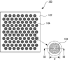
- FIG. 1 is a plan view schematically showing the structure of a sensing chip according to an embodiment of the invention.
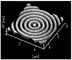
- FIG. 2 is an AFM (Atomic Force Microscope) image showing a concentric bull's eye structure, which is an example of a plasmon forming region.
- FIG. 3 is a cross-sectional view showing the structure of the sensing chip shown in FIG.
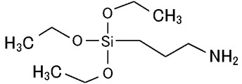
- FIG. 4 is a diagram showing the chemical formula of APTES (3-Aminopropyltriethoxysilane).
- FIG. 5 is a diagram showing a state in which the surface (SiO 2 ) of the chip body is modified with APTES.
- FIG. 1 is a plan view schematically showing the structure of a sensing chip according to an embodiment of the invention.
- FIG. 2 is an AFM (Atomic Force Microscope) image showing a concentric bull's eye structure, which is an example of a plasmon forming region.
- FIG. 3 is a cross-sectional view showing the structure of the sens
- FIG. 6 is a diagram showing a chemical formula of o-Methylbenzaldehyde, which is an example of a photoreactive compound.
- FIG. 7 is a diagram showing a state in which the o-Methylbenzaldehyde shown in FIG. 6 is combined with the chip body in the state shown in FIG.
- FIG. 8 is a diagram showing a state in which a maleimide compound is added to the chip body in the state shown in FIG.
- FIG. 9 is a diagram showing a state in which a photoreactive compound and a maleimide compound are bonded.
- FIG. 10 is a diagram showing another manufacturing method of the sensing chip.
- FIG. 11 is a diagram showing the chemical formula of Succinimidyl PEG.
- FIG. 12 is a block diagram showing a schematic configuration of the measuring device.
- FIG. 13 is a plan view showing an example of a periodic structure of a plasmon formation region different from the bull's eye structure.
- FIG. 14 is a plan view showing another example of the periodic structure of the plasmon formation region different from that of FIG.
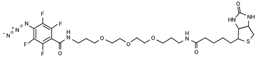
- FIG. 15 is a diagram showing the chemical formula of TFPA-PEG3-Biotin, which is an example of a photoreactive compound.
- FIG. 16 shows the photoreaction of TFPA-PEG3-Biotin shown in FIG.
- FIG. 17 is a plan view showing the structure of a prototype sensing chip.
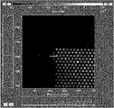
- FIG. 18 is a photograph showing experimental results.
- FIG. 13 is a plan view showing an example of a periodic structure of a plasmon formation region different from the bull's eye structure.
- FIG. 14 is a plan view showing another example of the periodic structure of the plasmon formation region different from that of FIG.
- FIG. 15 is a
- FIG. 19 is a diagram showing a state in which Cy5-streptavidin was introduced as a target substance onto a substrate to which biotin-maleimide containing capture molecules was bound, in relation to Example 3.
- FIG. FIG. 20 is a diagram showing a state in which injected Cy5-streptavidin binds to biotin-maleimide bound to a substrate.
- FIG. 21 shows the result of observing fluorescence using a chip produced by irradiating UV light for causing a photoreaction, relating to Example 3.
- FIG. FIG. 22 shows the results of observation of fluorescence using a chip that was irradiated with UV light for causing a photoreaction and was fabricated under conditions different from those of the chip that produced the results of FIG.
- FIG. 23 is a photograph showing, as a comparative example, the result of observing fluorescence without irradiating the chip with UV light for causing a photoreaction.
- FIG. 24 shows the result of observing fluorescence after irradiating the chip with visible light for causing a photoreaction, relating to Example 4.
- FIG. 25 is a photograph showing the result of fluorescence observation using a chip fabricated without irradiation of light for promoting photoreaction and addition of Cy5-maleimide.
- FIG. 26 is a photograph showing the results of observing fluorescence using a chip fabricated by adding Cy5-maleimide without irradiating light for promoting photoreaction.
- FIG. 27 is a photograph showing the result of observing fluorescence using a chip produced by irradiating visible light for promoting photoreaction and adding Cy5-maleimide, in Example 5.
- FIG. 25 is a photograph showing the result of observing fluorescence using a chip produced by irradiating
- sensing chip 100 includes chip body 102 and plasmon generation region 104 formed on chip body 102 .
- a plurality of plasmon generation regions 104 are arranged in a hexagonal lattice.
- One plasmon generation region 104 is shown enlarged in the lower right of FIG.
- a bull's eye structure see the AFM image shown in FIG. 2 in which periodic unevenness is concentrically formed in a circular region with a diameter ⁇ is adopted.
- FIG. 3 shows a cross-sectional view of the plasmon generation region 104 shown in the lower right of FIG. 1, taken along line III-III passing through its center.
- the plasmon generation region 104 includes a base substrate 106 having the above-described periodic structure (that is, a bull's eye structure), a first adhesion layer 110 formed on the base substrate 106, a metal layer 112, a second 2 a multilayer film including an adhesive layer 114 and a quenching suppression layer 116 .
- Plasmon-generating region 104 further includes a binding compound 200 disposed over the multilayer film and a capture molecule 202 bound to binding compound 200 .
- the binding compound 200 is a compound in which a plurality of substances are bound by a photoreaction (that is, a photochemical reaction) using an enhanced electric field due to plasmon resonance, which will be described later.
- the trapping molecules 202 are unevenly distributed over the plasmon-generating region 104 although they may also exist in the area surrounding the plasmon-generating region 104 . That is, the trapping molecules 202 bind to the plasmon-generating region 104 at a higher density than the surrounding area of the plasmon-generating region 104 .
- the base substrate 106 is made of, for example, glass or plastic (such as polymethylmethacrylate (PMMA), etc.). Base substrate 106 may be transparent or opaque.
- the periodic structure can be formed by a known method (nanoprinting, press molding using a stamper (mold), injection molding, etc.).
- the period of the concentric periodic structure (the sum of the widths of adjacent recesses and protrusions) L1 is constant.
- the bull's eye structure shown in FIG. 3 has a convex shape with a central portion having a diameter L2 (a circle whose center is the center of the concentric circles of the periodic structure).
- L2 a circle whose center is the center of the concentric circles of the periodic structure.
- the central portion of the bullseye structure penetrates including the substrate, but in the plasmon generation region 104 the central portion does not penetrate.
- the period L1 is preferably less than or about the wavelength of light used for fluorescence observation.
- the period L1 is, for example, 100-1000 nm, preferably 200-600 nm.
- the diameter L2 of the central portion of the bull's eye structure is preferably equal to half the period L1 as shown in FIG. Well, it doesn't have to be equal.
- the diameter L2 may be equal to or less than the period L1.
- the central portion of the bull's eye structure may be concave.
- the concave diameter L2 may or may not be equal to half the period L1.
- the first adhesive layer 110 is a layer for bonding the base substrate 106 and the metal layer 112 together. If the base substrate 106 itself is made of a material that is stably fixed to the metal layer 112, the first adhesive layer 110 may be omitted. Also, the second adhesive layer 114 is a layer for bonding the metal layer 112 and the quenching suppressing layer 116 together. If the quenching suppressing layer 116 itself is made of a material that can be stably fixed to the metal layer 112, the second adhesive layer 114 may be omitted. Also, as will be described later, the quenching suppressing layer 116 may be omitted.
- the first adhesive layer 110 and the second adhesive layer 114 are preferably as thin as possible, and are formed as thin films of titanium (Ti) with a thickness of 0.1 to 3 nm, for example.
- Ti titanium
- the first adhesion layer 110 may be chromium (Cr).
- the metal layer 112 is silver (Ag), for example, and is formed by sputtering or the like.
- the film thickness of the metal layer (Ag) 112 is preferably 10-100 nm, more preferably 30-65 nm.
- FIG. 3 shows the shape of the metal layer 112 in the same manner as the uneven shape of the base substrate 106, but if the metal layer 112 is formed by sputtering or the like, it corresponds to the step portion of the periodic structure of the base substrate 106. part is slanted. Therefore, the second adhesive layer 114 and the quenching suppressing layer 116, which will be described later, can also have a sloped shape.
- the quenching suppression layer 116 is also a layer for binding capture molecules (eg, antibodies), and is preferably formed of silicon dioxide (SiO 2 ) so that commercially available bioassay kits (eg, drugs) can be used. . Many commercially available chemicals are intended for application to SiO 2 . SiO 2 has no absorption (or low absorption) in the wavelength regions of incident light and generated fluorescence normally used for observation, so it can be formed as a transparent thin film.
- the quenching suppression layer 116 can be formed by sputtering, for example.
- the enhanced fluorescence which is a feature of the surface plasmon excitation enhanced fluorescence method, is quenched by energy transfer to the metal surface when the fluorescent molecules and the metal layer 112 are close together. Therefore, it is preferable to separate the fluorescent molecules from the metal layer 112 by a predetermined distance to suppress quenching. Therefore, if the molecular layer of the binding compound 200 and the capture molecule 202 shown in FIG. 3 has an appropriate thickness, the quenching suppression layer 116 may be omitted.
- the excitation field by surface plasmon resonance is a near field, the electric field strength is attenuated as the distance from the metal surface increases, so only fluorescent molecules existing within about 100 nm from the surface of the metal layer 112 are efficiently excited. be.
- the film thickness of the quenching suppressing layer 116 is determined within the range of about 10 nm to 100 nm according to the type of the metal layer 112, the refractive index of the quenching suppressing layer 116, the wavelength of the incident light, and the like.
- the multilayer film formed on the base substrate 106 may include a protective layer in addition to the above.
- the total thickness of the protective layer and the quenching suppressing layer 116 is in the range of about 10 nm to 100 nm. It is preferably determined according to the refractive index of the layer 116, the wavelength of the incident light, and the like.
- the sensing chip 100 is used to detect antigen-antibody reactions.
- the capture molecule 202 preferably corresponds to the antigen to be captured, that is, to generate an antigen-antibody reaction with the antigen to be captured.
- capture molecules 202 bound to the surface of the plasmon generation region 104 (that is, the quenching suppressing layer 116) via the binding compound 200 and the injected antigen
- An antigen-antibody reaction occurs.
- a fluorescence-labeled protein ie, fluorescent molecule
- the binding compound 200 and the capture molecule 202 may be non-specifically adsorbed around the plasmon generation region 104 as well, so fluorescence is emitted therefrom as well.
- fluorescence can be noise, but is small compared to the enhanced fluorescence intensity emitted from the plasmon generation region 104 . Therefore, the sensing chip 100 enables highly sensitive detection.
- the manufacturing method of the sensing chip 100 includes steps 1 to 4 below.
- Step 1 Place APTES (see FIG. 4) on the chip body 102 by silane coupling.
- the terminus of APTES that is not bound to the substrate is an amino group.
- FIG. 5 shows a state in which the surface of the quenching suppressing layer 116 of the chip body 102 and the APTES 210 are silane-coupled.
- Step 2 A photoreactive compound is introduced into the chip body 102 on which step 1 has been performed, and the photoreactive compound is bonded to the amino group of APTES (amide bond).
- APTES amide bond
- o-Methylbenzaldehyde hereinafter also referred to as benzaldehyde
- the addition of the photoreactive compound is performed by preparing a DMF solution. That is, a solution is prepared by adding TEA (triethylamine), EDC (1-ethyl-3-(3-dimethylaminopropyl) carbodiimide hydrochloride), and a photoreactive compound to DMF (N,N-dimethylformamide).
- step 1 This is placed on the substrate on which step 1 has been performed, and allowed to stand for a predetermined time (for example, 2 hours). Due to the dehydration reaction, APTES and o-Methylbenzaldehyde form an amide bond as shown in FIG.
- Step 3 As shown in FIG. 8, a maleimide compound modified with a capture molecule (antibody) is introduced into the chip body 102 on which step 2 has been performed, and light (for example, ultraviolet light (hereinafter referred to as UV light) is applied from the back of the substrate. )) is irradiated for a predetermined time (for example, 5 minutes).
- FIG. 8 shows N-succinimidyl-3-maleimidopropionate 214 modified with capture molecule 202 as the maleimide compound. By irradiating light, an enhanced electric field is formed by plasmons in the plasmon generation region 104 .
- FIG. 9 shows a state in which an o-methylbenzaldehyde group and a maleimide group are bonded.
- Step 4 Wash the chip body 102 for which step 3 has been performed.
- a mixed phosphate buffer solution ie, Tween 20
- Tween 20 which is a surfactant
- the photoreaction between the photoreactive compound (ie benzaldehyde 212) and the maleimide compound (ie N-succinimidyl-3-maleimidopropionate 214) is not promoted in the area surrounding the plasmon generating region 104 . Unreacted maleimide compound (ie, N-succinimidyl-3-maleimidopropionate 214) is removed from tip body 102 by washing.
- the sensing chip 100 in which the capture molecules 202 are site-selectively bound to the specific region (that is, the plasmon generation region 104) of the chip body 102 is realized. That is, in the sensing chip 100 , the capture molecules 202 are bound to the plasmon generation region 104 with a higher density than the surrounding region of the plasmon generation region 104 .
- a characteristic point is that the plasmon-generating region 104 is irradiated with light to promote a photoreaction using an enhanced electric field due to plasmons in the plasmon-generating region 104 , so that the plasmon-generating region 104 is intensively bound to the capture antibody.
- a significant fluorescence enhancement effect can be obtained.
- binding of the capture antibody can be suppressed, so detection sensitivity is improved.
- N-succinimidyl-3-maleimidopropionate 214 modified with capture molecules 202 is added to chip body 102 in a state where compounds of APTES 210 and benzaldehyde 212 are bound, and a chemical reaction occurs due to plasmon resonance.
- a photoreactive compound ie, benzaldehyde 212
- a capture molecule 202 is introduced into a chip body 102 in a state where compounds of APTES 210 and N-succinimidyl-3-maleimidopropionate 214 are bound. , may be irradiated with UV light.
- a plasmon-enhanced electric field is formed in the plasmon-generating region 104 to promote photoreaction between the photoreactive compound (ie, benzaldehyde 212) and the maleimide compound (ie, N-succinimidyl-3-maleimidopropionate 214). Therefore, as in FIG.
- the photoreactive compound ie, benzaldehyde 212
- the maleimide compound ie, N-succinimidyl-3-maleimidopropionate 214
- the specific region of the chip body 102 ie, A sensing chip 100 is fabricated in which capture molecules 202 are site-selectively bound to the plasmon generating region 104.
- the photoreactive compound that is, benzaldehyde 212
- the succinimidyl PEG having a carboxyl-terminated end shown in FIG. good can non-specifically adsorb to the chip body 102 in addition to binding to the photoreactive compound.
- an antigen-antibody reaction occurs with capture molecules (for example, antibodies) non-specifically adsorbed to the chip body 102, and fluorescence is also emitted from the area surrounding the plasmon generation area 104. It causes a decrease in detection sensitivity.
- succinimidyl PEG it can be expected that non-specific adsorption of the capture molecule-modified maleimide compound to the chip body 102 in step 3 can be suppressed.
- a localized plasmon-enhanced electric field can be formed in a partial region of the plasmon generation region 104, it can be expected that the above-described photoreaction is intensively promoted in a partial region of the plasmon generation region 104.
- an enhanced electric field can be formed by localized plasmons due to the optical antenna effect at the center of the bullseye structure. Therefore, capture molecules can bind to the central portion of the plasmon generation region 104 at a higher density than the surrounding regions.
- the plasmon generation region 104 In order to bind the trapping molecules to the central portion of the plasmon generation region 104 at high density, it is preferable to irradiate the plasmon generation region 104 with light in the visible region (380 nm to 780 nm) instead of UV light, for example. Normally, even if the light in the visible region is irradiated, the effect of accelerating the photoreaction is small. On the other hand, by irradiating the plasmon generation region 104 with light in the visible light region, the plasmons can be localized in the central portion of the plasmon generation region 104, and the light can be concentrated in the central portion of the plasmon generation region 104. This is because the reaction can be accelerated.
- a solution containing microspheres whose surface is modified with a capture antibody for example, silica beads with a diameter of 1 ⁇ m or less
- a biotin compound, or streptavidin bound with a capture antibody is put into the chip body 102, and the Visible light of 550 nm or 600 nm to 1100 nm is irradiated.
- silica beads, a biotin compound, or the like can be intensively bound to the central portion of the plasmon generation region 104 .
- Visible light from 300 nm to 550 nm can be used to promote single photon photoreactions, and visible light from 600 nm to 1100 nm (eg, 720 nm) can be used to promote two photon photoreactions.
- the sensing chip thus produced, for example, if a fluorescently-labeled antigen is introduced, it becomes possible to observe the antigen-antibody reaction with higher sensitivity by fluorescence.
- the chip body 102 having the plasmon generation region 104 described above can constitute a sensing kit together with the photoreactive compound.
- a photoreactive compound is injected onto the chip body 102 and irradiated with light, thereby promoting the photoreaction by the enhanced electric field caused by the plasmon, and the plasmon generation region 104
- the photoreactive compound can be bound intensively to the .
- measuring device 400 Manufacture of the sensing chip 100 and an apparatus used for fluorescence observation using the sensing chip 100 will be described.
- measuring device 400 includes sensing chip 100 , light source 402 , optical filter 404 , first lens 406 , second lens 408 and camera 410 .
- sensing chip 100 shown in FIG.
- a light source 402 is a mercury lamp or a halogen lamp.
- the optical filter 404 allows light of a specific wavelength out of the light emitted from the light source 402 to pass through and blocks other light.
- a Cy5 filter that is, a bandpass filter that passes the excitation light of the fluorescent substance Cy5
- a NUA filter that is, a bandpass filter that passes wavelengths of 370 to 380 nm
- a first lens 406 is an objective lens for converging light that has passed through the optical filter 404 .
- the first lens 406 is, for example, a 20-fold objective lens.
- a halogen lamp is used as the light source 402
- a Cy5 filter is used as the optical filter 404 if the sensing chip 100 is modified with molecules fluorescently labeled with Cy5, for example.
- the first lens 406 has, for example, A 100x magnification objective is used.
- a mercury lamp is used as the light source 402 and a NUA filter is used as the optical filter 404 .
- the second lens 408 is a lens that converges fluorescence emitted from the sensing chip 100 and outputs it to the camera 410 .
- the second lens 408 is, for example, a lens with a magnification of 10 times.
- Camera 410 is an imaging device (for example, a CCD camera). Note that the measurement apparatus 400 may include an optical system (for example, a prism, a mirror, etc.) other than the configuration shown in FIG.
- the local photoreaction within the pattern can be promoted in the plasmon generation region 104 of the concentric periodic structure.
- This photoreaction between a compound having a maleimide group and a photoreactive compound can be realized with light in a wavelength range from UV light to visible light. Especially in the near-infrared region, a two-photon reaction can be expected.
- a strong electric field is formed especially in the central portion, so that it is possible to form a local electric field especially in the central portion even within the pattern. It is believed that the local photoreaction can realize highly sensitive detection in immunoassay construction.
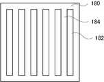
- the periodic structure of the plasmon generation region 104 may be one in which periodic unevenness is formed in parallel along one direction as shown in FIG. 13 (that is, a Line & Space pattern).
- a convex portion 182 is formed parallel to one direction on the surface of a base substrate 180
- a concave portion 184 is formed around the convex portion 182 .
- a two-dimensional periodic structure as shown in FIG. 14 may be used.
- projections 192 are formed in two directions intersecting the surface of a base substrate 190
- recesses 194 are formed around the projections 192 . 13, or a hole array with the unevenness reversed in FIG. 14 may be used.
- the cross-sectional shape of the concave portion (groove) of the periodic structure of the plasmon generation region 104 is not limited to, for example, the rectangular shape shown in FIG.
- the metal layer 112 is not limited to silver (Ag), and any metal that causes surface plasmon resonance may be used.
- the metal layer 112 may be gold (Au), aluminum (Al), or the like.
- o-Methylbenzaldehyde (see FIG. 6) is shown above as a photoreactive compound, it is not limited to this.
- Commercially available reagents and the like can also prepare the interface by photoreaction with the APTES surface.
- TFPA-PEG3-Biotin shown in FIG. 15 can be used as the photoreactive compound.
- TFPA-PEG3-Biotin With APTES 210 bound to the surface of chip body 102, TFPA-PEG3-Biotin is added and UV light is applied. As a result, in the plasmon generation region 104, the photoreaction shown in FIG. Therefore, TFPA-PEG3-Biotin can be intensively bound to APTES 210 bound to the plasmon-generating region 104 . Then, TFPA-PEG3-Biotin is bound to an avidin-modified antibody or avidin+biotin-modified antibody to prepare the sensing chip 100 having the structure shown in FIG.
- a compound represented by the following general formula (1) or general formula (2) may also be used as the photoreactive compound.
- R is any one of the following compounds A1 to A11.
- general formula (1) is 3-((2-formyl-3-methylphenyl)thio)propanoic acid, that is, o-methylbenzaldehyde shown in FIG.
- the binding compound 200 that binds the capture molecule 202 to the chip body 102 is not limited to including APTES 210 bound to the quenching suppression layer 116 .
- the binding compound 200 is formed by a photoreaction of a photoreactive compound in the manufacturing process of the sensing chip 100 and is bound to the quenching suppressing layer 116 . Photoreaction of the photoreactive compound allows it to concentrate in the plasmon generating region 104 to bind the binding compound 200 and thus the capture molecule 202 .
- the object (target substance) captured by the capturing molecules 202 is not limited to antigens, and may be DNA or the like.
- the capture molecule 202 may be any molecule for capturing the target substance. Capture molecule 202 may be, for example, a compound having a portion that specifically adsorbs to a target substance.
- a chip having the structure shown in FIG. 17 was fabricated. About 2000 plasmon generating regions 104 were formed only in the upper left region of the chip body 102 .
- the plasmon generation region 104 has an outer diameter of 20 ⁇ m, a period of 480 nm (that is, the interval between adjacent convex portions is 240 nm), and a convex shape with a diameter of 480 nm at the central portion.
- the plurality of plasmon generation regions 104 are arranged in a hexagonal lattice with an adjacent spacing of 5 ⁇ m (therefore, a center spacing of 25 ⁇ m).
- a multilayer film was formed as described above on the base substrate on which such a plasmon generation region 104 was formed. That is, the first and second adhesion layers were each formed using Ti to a thickness of less than 1 nm, the metal layer was formed using Ag to a thickness of 45 nm, and the quenching suppression layer was formed using SiO 2 to a thickness of 20 nm.
- a chip body 102 having a plasmon generation region 104 as described above was prepared, and a chip modified with a compound was manufactured in the same manner as in the manufacturing method described above. Specifically, after binding APTES (see FIG. 5) to the chip body, o-Methylbenzaldehyde (see FIG. 6) was added as a photoreactive compound and allowed to stand for 2 hours. let me For DMF solution preparation, 2 mL of DMF, 15 ⁇ L of TEA, 11.5 mg of EDC, and 11.2 mg of o-Methylbenzaldehyde were used. These operations were performed in a dark room or a yellow lamp room.
- Fluorescent observation was performed using the fabricated chip.
- the halogen lamp and Cy5 filter described above were used as the light source and optical filter, respectively, and the light passing through the Cy5 filter was focused using a 20x objective lens and irradiated onto the back surface of the chip.
- the fluorescence emitted from the chip was focused using a 20x objective lens and observed with a CCD camera.
- FIG. 18 The image captured by the CCD camera is shown in FIG.
- the circle (that is, the white dashed line) shown in the center indicates the boundary of the area irradiated with light for promoting the photoreaction during chip manufacture.
- the dashed circle shown in the center corresponds to the circle shown in the center of FIG.
- almost no fluorescence is observed from the region where the plasmon generation region 104 is not formed.
- fluorescence can be observed due to an enhanced electric field by plasmons. It can be seen that the fluorescence intensity from the plasmon generation region 104 formed inside the dashed circle (see FIG. 17) is stronger than the plasmon generation region 104 formed around it. From this, it was confirmed that the binding of Cy5-maleimide to the plasmon generation region 104 was promoted by irradiating light for promoting the photoreaction during chip manufacture.
- Table 1 shows the fluorescence intensities measured for the four regions Birr, Bout, Firr and Fout as shown in FIG.
- Ef represents the effect of fluorescence enhancement by the plasmon generation region 104 .
- the region Birr is irradiated with light for promoting the photoreaction, and the region Bout is not irradiated with light for promoting the photoreaction. effects.
- Firr-Fout represents only the photoreaction promotion effect. Therefore, the chemical reaction promotion effect can be evaluated by dividing (Birr-Bout)/(Firr-Fout) by the fluorescence enhancement Ef as shown in Equation 2 above.
- the plasmon generation region 104 in the region Birr in FIG. 17 is formed over the entire surface of the actual sensing chip. That is, a sensing chip that does not include the regions Bout and Fout shown in FIG. 17 but includes the region Birr and a region corresponding to the region Firr (the region in which the plasmon generation region 104 is not formed) can be considered.
- Example 2 As a comparative example, a chip body similar to that of Example 1 was used and the same steps were performed, but without performing the step of irradiating UV light to promote the photoreaction, a chip was produced and fluorescence observation was performed. That is, in the same manner as in Example 1, APTES (see FIG. 5) and o-Methylbenzaldehyde (see FIG. 6) were put into the chip body 102 in which the plasmon generation region 104 was formed, and they were combined as shown in FIG. rice field.
- APTES see FIG. 5
- o-Methylbenzaldehyde see FIG. 6
- the fluorescence enhancement Ef and the chemical reaction acceleration rate Rp were calculated by the above formulas 1 and 2.
- the fluorescence enhancement Ef about 4.7
- Example 2 Using a chip produced in the same manner as in Example 1, an experiment was conducted to confirm that the target substance could be captured by the capture molecules bound to the chip. Specifically, a chip body (see FIG. 17) having the same structure, material and dimensions as those of Example 1 was prepared. In the same manner as in Example 1, APTES (see FIG. 5) was bound to the chip body, and then o-methylbenzaldehyde (see FIG. 6) was introduced as a photoreactive compound and bound as shown in FIG. . Subsequently, biotin-maleimide prepared to about 1 ⁇ M was added to the central portion of the chip body (corresponding to the dashed circle in FIG. 17) while irradiating UV light for 30 seconds to activate the photoreactive substance.
- APTES see FIG. 5
- o-methylbenzaldehyde see FIG. 6
- biotin-maleimide prepared to about 1 ⁇ M was added to the central portion of the chip body (corresponding to the dashed circle in FIG. 17) while
- biotin as a capture molecule was bound to the chip.
- the compounds of APTES 210, benzaldehyde 212 and biotin-maleimide 300 are bound to the plasmon generating region 104.
- a protein fluorescently labeled with Cy5 specifically, streptavidin
- Cy5-streptavidin 312 was applied to the chip to which the biotin portion 302 was bound.
- a complex in which biotin portion 302 is bound to Cy5-streptavidin 312 is formed by the interaction of biotin and avidin. That is, the Cy5-streptavidin 312 is bound to the plasmon-generating region 104 .
- FIGS. 21 and 22 Images captured by the CCD camera are shown in FIGS. 21 and 22.
- FIG. Figures 21 and 22 correspond to chips made with Cy5-streptavidin 312 doses adjusted to about 10 nM and 1 nM, respectively.
- the bar shown in the bottom right of FIG. 22 represents a length of 100 ⁇ m.
- FIGS. 21 and 22 almost no fluorescence is observed from the regions where the plasmon generation regions are not formed. In the plasmon generation region, fluorescence can be observed due to an enhanced electric field by plasmons. It can be seen that the fluorescence intensity from the plasmon generation region in the center of each chip is stronger than the plasmon generation region formed around it.
- FIG. 6 As a comparative experiment, using the same chip body as above, o-Methylbenzaldehyde (see FIG. 6) was added after binding APTES to the chip body, and without irradiation with UV light for promoting the photoreaction. Biotin-maleimide was loaded. Biotin as a capture molecule thereby binds to the chip by non-specific adsorption. Fluorescence observation was performed in the same manner as in Example 1 using the fabricated chip. An image captured by the CCD camera is shown in FIG. In FIG. 23, fluorescence could be observed almost uniformly in the plasmon generation region due to the enhanced electric field due to plasmons. A comparison of FIGS. 21 and 23 shows the effectiveness of UV light irradiation for promoting the photoreaction during chip fabrication. That is, the capturing molecules can be spatially selectively bound to the chip, and the detection accuracy of the target substance by the capturing molecules is improved.
- the chip interface was prepared using visible light as the light to promote the photoreaction. Specifically, a chip body (see FIG. 17) having the same material and dimensions as those of Example 1 was prepared except for the structure of the central portion of each plasmon generation region. The central portion has a concave structure (that is, a well structure) with a size of 1/2 pitch, and the unevenness is reversed from the shape shown in FIG. o-Methylbenzaldehyde (see FIG. 6) was bonded to the chip (see FIG. 7) as in Example 1, using visible light (specifically wavelength 450 nm to 490 nm) instead of UV light. At the time of light irradiation, in the configuration shown in FIG. GFP light).
- visible light specifically wavelength 450 nm to 490 nm
- Cy5-maleimide prepared at 9.36 nM was loaded and allowed to bind to the chip. Fluorescence observation was performed in the same manner as in Example 1 using the fabricated chip. An image captured by the CCD camera is shown in FIG. The bar shown in the bottom right of FIG. 24 represents a length of 50 ⁇ m. Fluorescence observation was performed with the configuration shown in FIG. 12, a halogen lamp was used as the light source 402, and objective lenses with magnifications of 20 ⁇ and 10 ⁇ were used as the first lens 406 and the second lens 408, respectively. Table 3 shows the fluorescence intensities measured for the four regions Birr, Bout, Firr and Fout as shown in FIG.
- Ef 12.9 was obtained.
- the chemical reaction acceleration rate Rp calculated by Equation 2 above cannot be calculated from the values in Table 3, since the values of Firr and Fout are both "8". That is, by manufacturing a chip using GFP light as light for promoting photoreaction, the fluorescence intensity in regions other than the plasmon-generating region was approximately the same regardless of whether or not GFP light was irradiated. . From this, it can be seen that by using GFP light, binding of the capture molecules to regions other than the plasmon generation region can be suppressed, and the capture molecules can be spatially selectively bound only to the plasmon generation region.
- GFP light with a wavelength of 450 nm to 490 nm corresponds to the absorption edge of o-Methylbenzaldehyde (see FIG. 6) used as a photoresponsive substance, and photoreaction hardly occurred.
- each plasmon generation region By using visible light as light to promote the photoreaction, experiments were conducted to confirm that capture molecules could be densely bound to the center of each plasmon generation region. Specifically, a chip body (see FIG. 17) having the same structure, material and dimensions as those of Example 4 was prepared. The central portion of each plasmon generation region is a concave structure with a size of 1/2 pitch. As in Example 4, o-Methylbenzaldehyde (see FIG. 6) was bound to the chip using GFP light (wavelength 450 nm to 490 nm) as light for promoting the photoreaction. Subsequently, Cy5-maleimide adjusted to 9.36 nM was added, followed by washing with PBS (phosphate buffer). The manufactured chip is called a chip of Example 5.
- GFP light wavelength 450 nm to 490 nm
- the same chip body (see FIG. 17) as above was prepared, and o-Methylbenzaldehyde (see FIG. 6) was put into the chip without irradiating light for promoting the photoreaction. No Cy5-maleimide was input.
- the manufactured chip is called a chip of the first comparative example.
- the same chip body (see FIG. 17) as above was prepared, and o-Methylbenzaldehyde (see FIG. 6) was put into the chip without irradiating light for promoting the photoreaction. Subsequently, Cy5-maleimide adjusted to 9.36 nM was added, followed by washing with PBS.
- the manufactured chip is called a chip of a second comparative example.
- FIGS. 25 to 27 Fluorescent images captured by the CCD camera are shown in FIGS. 25 to 27.
- FIG. 25 to 27 are images of the chip of the first comparative example, the chip of the second comparative example, and the chip of Example 5, respectively, and the corresponding regions are captured.
- the bar shown in the bottom right of each figure represents a length of 20 ⁇ m. Fluorescence observation was performed with the configuration shown in FIG. 12, a mercury lamp was used as the light source 402, and objective lenses with magnifications of 20 ⁇ and 100 ⁇ were used as the first lens 406 and the second lens 408, respectively.
- the fluorescence intensity B (BKG) in the plasmon generation region and the fluorescence intensity F (BKG) outside the plasmon generation region were "540" and "523", respectively. All measured values, including those indicated below, are relative values expressed on the same basis.
- BKG means background
- B(BKG) and F(BKG) are the levels of background noise inside and outside the plasmon generation region, respectively.
- the fluorescence intensity in the plasmon generation region is clearly increased in the fluorescence image in FIG.
- the fluorescence intensity at the center is clearly higher than the fluorescence intensity at the periphery.
- the fluorescence intensity Bc (irradiation) at the center of the plasmon generation region, the fluorescence intensity Be (irradiation) at the periphery of the plasmon generation region, and the fluorescence intensity F (irradiation) outside the plasmon generation region are respectively " 890", "710" and "543".
- "irradiation” represents not irradiating the light for promoting a photoreaction.
- the chip of Example 5 contains Cy5-maleimide bound by photoreaction in addition to Cy5-maleimide bound by non-specific adsorption.
- ⁇ Bc (irradiated) and ⁇ Be (irradiated) for the chip of Example 5 are larger than ⁇ Bc (unirradiated) and ⁇ Be (unirradiated) for the chip of Comparative Example 2, respectively, due to the photoreaction.
- sensing chip 102 chip body 104 plasmon generating regions 106, 180, 190 base substrate 110 first adhesive layer 112 metal layer 114 second adhesive layer 116 quenching suppressing layers 182, 192 convex portions 184, 194 concave portion 200 binding compound 202 capture molecule 210 APTES 212 benzaldehyde 214 N-succinimidyl-3-maleimidopropionate 300 biotin-maleimide 302 biotin moiety 304 maleimide moiety 312 Cy5-streptavidin 400 measuring device 402 light source 404 optical filter 406 first lens 408 second lens 410 camera Birr, Bout, Firr, Fout Area L1 Period L2, ⁇ Diameter
Landscapes
- Health & Medical Sciences (AREA)
- Physics & Mathematics (AREA)
- Life Sciences & Earth Sciences (AREA)
- Chemical & Material Sciences (AREA)
- Analytical Chemistry (AREA)
- Biochemistry (AREA)
- General Health & Medical Sciences (AREA)
- General Physics & Mathematics (AREA)
- Immunology (AREA)
- Pathology (AREA)
- Nuclear Medicine, Radiotherapy & Molecular Imaging (AREA)
- Investigating, Analyzing Materials By Fluorescence Or Luminescence (AREA)
Abstract
La puce de détection de l'invention comprend un substrat comportant une région de génération de plasmons avec une structure périodique, et une pluralité de molécules de capture pour capturer une substance cible. La pluralité de molécules de capture est liée à la région de génération de plasmons à une densité plus élevée que dans une région autour de la région de génération de plasmons. La sensibilité de détection de l'observation par fluorescence est ainsi plus élevée qu'auparavant.
Priority Applications (1)
| Application Number | Priority Date | Filing Date | Title |
|---|---|---|---|
| JP2023502208A JPWO2022181196A1 (fr) | 2021-02-26 | 2022-01-28 |
Applications Claiming Priority (2)
| Application Number | Priority Date | Filing Date | Title |
|---|---|---|---|
| JP2021029652 | 2021-02-26 | ||
| JP2021-029652 | 2021-02-26 |
Publications (1)
| Publication Number | Publication Date |
|---|---|
| WO2022181196A1 true WO2022181196A1 (fr) | 2022-09-01 |
Family
ID=83049208
Family Applications (1)
| Application Number | Title | Priority Date | Filing Date |
|---|---|---|---|
| PCT/JP2022/003209 WO2022181196A1 (fr) | 2021-02-26 | 2022-01-28 | Puce de détection, procédé de fabrication de puce de détection, kit de détection, procédé de mesure et dispositif de mesure |
Country Status (2)
| Country | Link |
|---|---|
| JP (1) | JPWO2022181196A1 (fr) |
| WO (1) | WO2022181196A1 (fr) |
Citations (8)
| Publication number | Priority date | Publication date | Assignee | Title |
|---|---|---|---|---|
| JP2004093558A (ja) * | 2002-07-12 | 2004-03-25 | Mitsubishi Chemicals Corp | 分析用チップ、分析用チップユニット及び分析装置ならびに分析用チップの作製方法 |
| JP2009503548A (ja) * | 2005-08-02 | 2009-01-29 | ユニバーシティ・オブ・ユタ・リサーチ・ファウンデイション | 金属ナノキャビティを含むバイオセンサー |
| JP2010540900A (ja) * | 2007-09-18 | 2010-12-24 | アプライド バイオシステムズ インコーポレイテッド | 集光機構のための方法、システムおよび装置 |
| JP2012026923A (ja) * | 2010-07-26 | 2012-02-09 | Konica Minolta Holdings Inc | Spfs(表面プラズモン励起増強蛍光分光法)またはそれを用いた測定法用の表面プラズモン励起センサ、それを作製するためのキットならびに表面プラズモン励起センサを備えたspfsまたはそれを用いた測定法用測定装置 |
| JP2013029369A (ja) * | 2011-07-27 | 2013-02-07 | Konica Minolta Holdings Inc | イオン性官能基で修飾された局在場光センサーチップおよびリガンド担持荷電微粒子を使用するアナライトの検出方法 |
| JP2013178224A (ja) * | 2012-01-31 | 2013-09-09 | National Institute Of Advanced Industrial & Technology | バイオチップ、バイオアッセイ用キット、及びバイオアッセイ方法 |
| JP2019509497A (ja) * | 2016-02-02 | 2019-04-04 | 学校法人沖縄科学技術大学院大学学園 | アミノシランを用いるマイクロ及びナノコンタクトプリンティング:多重バイオアッセイのためのマイクロ流体デバイスのパターニング表面 |
| JP2020153904A (ja) * | 2019-03-22 | 2020-09-24 | パナソニックIpマネジメント株式会社 | センサ基板の製造方法、センサ基板および検出装置 |
-
2022
- 2022-01-28 WO PCT/JP2022/003209 patent/WO2022181196A1/fr active Application Filing
- 2022-01-28 JP JP2023502208A patent/JPWO2022181196A1/ja active Pending
Patent Citations (8)
| Publication number | Priority date | Publication date | Assignee | Title |
|---|---|---|---|---|
| JP2004093558A (ja) * | 2002-07-12 | 2004-03-25 | Mitsubishi Chemicals Corp | 分析用チップ、分析用チップユニット及び分析装置ならびに分析用チップの作製方法 |
| JP2009503548A (ja) * | 2005-08-02 | 2009-01-29 | ユニバーシティ・オブ・ユタ・リサーチ・ファウンデイション | 金属ナノキャビティを含むバイオセンサー |
| JP2010540900A (ja) * | 2007-09-18 | 2010-12-24 | アプライド バイオシステムズ インコーポレイテッド | 集光機構のための方法、システムおよび装置 |
| JP2012026923A (ja) * | 2010-07-26 | 2012-02-09 | Konica Minolta Holdings Inc | Spfs(表面プラズモン励起増強蛍光分光法)またはそれを用いた測定法用の表面プラズモン励起センサ、それを作製するためのキットならびに表面プラズモン励起センサを備えたspfsまたはそれを用いた測定法用測定装置 |
| JP2013029369A (ja) * | 2011-07-27 | 2013-02-07 | Konica Minolta Holdings Inc | イオン性官能基で修飾された局在場光センサーチップおよびリガンド担持荷電微粒子を使用するアナライトの検出方法 |
| JP2013178224A (ja) * | 2012-01-31 | 2013-09-09 | National Institute Of Advanced Industrial & Technology | バイオチップ、バイオアッセイ用キット、及びバイオアッセイ方法 |
| JP2019509497A (ja) * | 2016-02-02 | 2019-04-04 | 学校法人沖縄科学技術大学院大学学園 | アミノシランを用いるマイクロ及びナノコンタクトプリンティング:多重バイオアッセイのためのマイクロ流体デバイスのパターニング表面 |
| JP2020153904A (ja) * | 2019-03-22 | 2020-09-24 | パナソニックIpマネジメント株式会社 | センサ基板の製造方法、センサ基板および検出装置 |
Also Published As
| Publication number | Publication date |
|---|---|
| JPWO2022181196A1 (fr) | 2022-09-01 |
Similar Documents
| Publication | Publication Date | Title |
|---|---|---|
| JP6301311B2 (ja) | 超高感度センサ | |
| Volkert et al. | Advancements in nanosensors using plastic antibodies | |
| JP5652393B2 (ja) | Spfs−lpfs系による測定方法に供するプラズモン励起センサおよびアッセイ法 | |
| JP6260541B2 (ja) | 夾雑物の影響を低減する免疫測定法 | |
| JP5772612B2 (ja) | 表面プラズモン励起増強蛍光分光法を利用する蛍光測定装置用センサチップを用いたアッセイ方法、およびアッセイ用キット | |
| Li et al. | Fluorescence enhancement enabled by nanomaterials and nanostructured substrates: A brief review | |
| JP5428322B2 (ja) | プラズモン励起センサを用いたアッセイ法 | |
| JP5958339B2 (ja) | 近接場増強蛍光センサチップ | |
| JP2010256161A (ja) | プラズモン励起センサおよびそれを用いたアッセイ法 | |
| JP5975480B2 (ja) | バイオチップ、バイオアッセイ用キット、及びバイオアッセイ方法 | |
| Vaschenko et al. | Enhancement of labeled alpha-fetoprotein antibodies and antigen-antibody complexes fluorescence with silver nanocolloids | |
| Rastogi et al. | Engineering electromagnetic hot-spots in nanoparticle cluster arrays on reflective substrates for highly sensitive detection of (bio) molecular analytes | |
| WO2022181196A1 (fr) | Puce de détection, procédé de fabrication de puce de détection, kit de détection, procédé de mesure et dispositif de mesure | |
| JP7445913B2 (ja) | 単一粒体分析用イムノセンサ及び単一粒体分析法 | |
| Kim et al. | Wash-free non-spectroscopic optical immunoassay by controlling retroreflective microparticle movement in a microfluidic chip | |
| JP2008096189A (ja) | 蛍光測定法と、蛍光測定のための測定用チップ及びその製造方法 | |
| JP2005189237A (ja) | 光学的測定方法 | |
| US20110195516A1 (en) | Wire grid substrate structure and method for manufacturing such a substrate | |
| JP5205293B2 (ja) | 抗体固定基板、並びに該抗体固定基板の製造方法及び利用 | |
| WO2012023391A1 (fr) | Capteur de spectroscopie par fluorescence renforcée par champ de plasmon de surface équipé d'un mécanisme de purification du type à adsorption non spécifique | |
| Shukla et al. | Nanoplasmonic biosensors: current perspectives | |
| Tawa et al. | Rapid and sensitive detection of brain-derived neurotrophic factor with a plasmonic chip | |
| JP2011127991A (ja) | プラズモン励起センサおよび該センサを用いたアッセイ法 | |
| WO2024034561A1 (fr) | Support en phase solide et kit de mesure d'objet cible | |
| JP5298877B2 (ja) | プラズモン励起センサを用いたアッセイ法 |
Legal Events
| Date | Code | Title | Description |
|---|---|---|---|
| 121 | Ep: the epo has been informed by wipo that ep was designated in this application |
Ref document number: 22759238 Country of ref document: EP Kind code of ref document: A1 |
|
| WWE | Wipo information: entry into national phase |
Ref document number: 2023502208 Country of ref document: JP |
|
| NENP | Non-entry into the national phase |
Ref country code: DE |
|
| 122 | Ep: pct application non-entry in european phase |
Ref document number: 22759238 Country of ref document: EP Kind code of ref document: A1 |