WO2022176491A1 - 撮像装置 - Google Patents
撮像装置 Download PDFInfo
- Publication number
- WO2022176491A1 WO2022176491A1 PCT/JP2022/001884 JP2022001884W WO2022176491A1 WO 2022176491 A1 WO2022176491 A1 WO 2022176491A1 JP 2022001884 W JP2022001884 W JP 2022001884W WO 2022176491 A1 WO2022176491 A1 WO 2022176491A1
- Authority
- WO
- WIPO (PCT)
- Prior art keywords
- region
- impurity
- impurity region
- imaging device
- conductivity type
- Prior art date
- Legal status (The legal status is an assumption and is not a legal conclusion. Google has not performed a legal analysis and makes no representation as to the accuracy of the status listed.)
- Ceased
Links
Images







Classifications
-
- H—ELECTRICITY
- H10—SEMICONDUCTOR DEVICES; ELECTRIC SOLID-STATE DEVICES NOT OTHERWISE PROVIDED FOR
- H10D—INORGANIC ELECTRIC SEMICONDUCTOR DEVICES
- H10D30/00—Field-effect transistors [FET]
- H10D30/01—Manufacture or treatment
- H10D30/021—Manufacture or treatment of FETs having insulated gates [IGFET]
-
- H—ELECTRICITY
- H10—SEMICONDUCTOR DEVICES; ELECTRIC SOLID-STATE DEVICES NOT OTHERWISE PROVIDED FOR
- H10D—INORGANIC ELECTRIC SEMICONDUCTOR DEVICES
- H10D30/00—Field-effect transistors [FET]
- H10D30/60—Insulated-gate field-effect transistors [IGFET]
-
- H—ELECTRICITY
- H10—SEMICONDUCTOR DEVICES; ELECTRIC SOLID-STATE DEVICES NOT OTHERWISE PROVIDED FOR
- H10D—INORGANIC ELECTRIC SEMICONDUCTOR DEVICES
- H10D84/00—Integrated devices formed in or on semiconductor substrates that comprise only semiconducting layers, e.g. on Si wafers or on GaAs-on-Si wafers
-
- H—ELECTRICITY
- H10—SEMICONDUCTOR DEVICES; ELECTRIC SOLID-STATE DEVICES NOT OTHERWISE PROVIDED FOR
- H10D—INORGANIC ELECTRIC SEMICONDUCTOR DEVICES
- H10D84/00—Integrated devices formed in or on semiconductor substrates that comprise only semiconducting layers, e.g. on Si wafers or on GaAs-on-Si wafers
- H10D84/01—Manufacture or treatment
- H10D84/0123—Integrating together multiple components covered by H10D12/00 or H10D30/00, e.g. integrating multiple IGBTs
- H10D84/0126—Integrating together multiple components covered by H10D12/00 or H10D30/00, e.g. integrating multiple IGBTs the components including insulated gates, e.g. IGFETs
-
- H—ELECTRICITY
- H10—SEMICONDUCTOR DEVICES; ELECTRIC SOLID-STATE DEVICES NOT OTHERWISE PROVIDED FOR
- H10D—INORGANIC ELECTRIC SEMICONDUCTOR DEVICES
- H10D84/00—Integrated devices formed in or on semiconductor substrates that comprise only semiconducting layers, e.g. on Si wafers or on GaAs-on-Si wafers
- H10D84/01—Manufacture or treatment
- H10D84/02—Manufacture or treatment characterised by using material-based technologies
- H10D84/03—Manufacture or treatment characterised by using material-based technologies using Group IV technology, e.g. silicon technology or silicon-carbide [SiC] technology
- H10D84/038—Manufacture or treatment characterised by using material-based technologies using Group IV technology, e.g. silicon technology or silicon-carbide [SiC] technology using silicon technology, e.g. SiGe
-
- H—ELECTRICITY
- H10—SEMICONDUCTOR DEVICES; ELECTRIC SOLID-STATE DEVICES NOT OTHERWISE PROVIDED FOR
- H10F—INORGANIC SEMICONDUCTOR DEVICES SENSITIVE TO INFRARED RADIATION, LIGHT, ELECTROMAGNETIC RADIATION OF SHORTER WAVELENGTH OR CORPUSCULAR RADIATION
- H10F39/00—Integrated devices, or assemblies of multiple devices, comprising at least one element covered by group H10F30/00, e.g. radiation detectors comprising photodiode arrays
- H10F39/011—Manufacture or treatment of image sensors covered by group H10F39/12
- H10F39/014—Manufacture or treatment of image sensors covered by group H10F39/12 of CMOS image sensors
-
- H—ELECTRICITY
- H10—SEMICONDUCTOR DEVICES; ELECTRIC SOLID-STATE DEVICES NOT OTHERWISE PROVIDED FOR
- H10F—INORGANIC SEMICONDUCTOR DEVICES SENSITIVE TO INFRARED RADIATION, LIGHT, ELECTROMAGNETIC RADIATION OF SHORTER WAVELENGTH OR CORPUSCULAR RADIATION
- H10F39/00—Integrated devices, or assemblies of multiple devices, comprising at least one element covered by group H10F30/00, e.g. radiation detectors comprising photodiode arrays
- H10F39/10—Integrated devices
- H10F39/12—Image sensors
-
- H—ELECTRICITY
- H10—SEMICONDUCTOR DEVICES; ELECTRIC SOLID-STATE DEVICES NOT OTHERWISE PROVIDED FOR
- H10F—INORGANIC SEMICONDUCTOR DEVICES SENSITIVE TO INFRARED RADIATION, LIGHT, ELECTROMAGNETIC RADIATION OF SHORTER WAVELENGTH OR CORPUSCULAR RADIATION
- H10F39/00—Integrated devices, or assemblies of multiple devices, comprising at least one element covered by group H10F30/00, e.g. radiation detectors comprising photodiode arrays
- H10F39/80—Constructional details of image sensors
- H10F39/802—Geometry or disposition of elements in pixels, e.g. address-lines or gate electrodes
- H10F39/8023—Disposition of the elements in pixels, e.g. smaller elements in the centre of the imager compared to larger elements at the periphery
-
- H—ELECTRICITY
- H10—SEMICONDUCTOR DEVICES; ELECTRIC SOLID-STATE DEVICES NOT OTHERWISE PROVIDED FOR
- H10F—INORGANIC SEMICONDUCTOR DEVICES SENSITIVE TO INFRARED RADIATION, LIGHT, ELECTROMAGNETIC RADIATION OF SHORTER WAVELENGTH OR CORPUSCULAR RADIATION
- H10F39/00—Integrated devices, or assemblies of multiple devices, comprising at least one element covered by group H10F30/00, e.g. radiation detectors comprising photodiode arrays
- H10F39/80—Constructional details of image sensors
- H10F39/803—Pixels having integrated switching, control, storage or amplification elements
- H10F39/8037—Pixels having integrated switching, control, storage or amplification elements the integrated elements comprising a transistor
-
- H—ELECTRICITY
- H10—SEMICONDUCTOR DEVICES; ELECTRIC SOLID-STATE DEVICES NOT OTHERWISE PROVIDED FOR
- H10F—INORGANIC SEMICONDUCTOR DEVICES SENSITIVE TO INFRARED RADIATION, LIGHT, ELECTROMAGNETIC RADIATION OF SHORTER WAVELENGTH OR CORPUSCULAR RADIATION
- H10F39/00—Integrated devices, or assemblies of multiple devices, comprising at least one element covered by group H10F30/00, e.g. radiation detectors comprising photodiode arrays
- H10F39/80—Constructional details of image sensors
- H10F39/803—Pixels having integrated switching, control, storage or amplification elements
- H10F39/8037—Pixels having integrated switching, control, storage or amplification elements the integrated elements comprising a transistor
- H10F39/80377—Pixels having integrated switching, control, storage or amplification elements the integrated elements comprising a transistor characterised by the channel of the transistor, e.g. channel having a doping gradient
-
- H—ELECTRICITY
- H10—SEMICONDUCTOR DEVICES; ELECTRIC SOLID-STATE DEVICES NOT OTHERWISE PROVIDED FOR
- H10F—INORGANIC SEMICONDUCTOR DEVICES SENSITIVE TO INFRARED RADIATION, LIGHT, ELECTROMAGNETIC RADIATION OF SHORTER WAVELENGTH OR CORPUSCULAR RADIATION
- H10F39/00—Integrated devices, or assemblies of multiple devices, comprising at least one element covered by group H10F30/00, e.g. radiation detectors comprising photodiode arrays
- H10F39/80—Constructional details of image sensors
- H10F39/807—Pixel isolation structures
-
- H—ELECTRICITY
- H10—SEMICONDUCTOR DEVICES; ELECTRIC SOLID-STATE DEVICES NOT OTHERWISE PROVIDED FOR
- H10F—INORGANIC SEMICONDUCTOR DEVICES SENSITIVE TO INFRARED RADIATION, LIGHT, ELECTROMAGNETIC RADIATION OF SHORTER WAVELENGTH OR CORPUSCULAR RADIATION
- H10F39/00—Integrated devices, or assemblies of multiple devices, comprising at least one element covered by group H10F30/00, e.g. radiation detectors comprising photodiode arrays
- H10F39/80—Constructional details of image sensors
- H10F39/811—Interconnections
-
- H—ELECTRICITY
- H10—SEMICONDUCTOR DEVICES; ELECTRIC SOLID-STATE DEVICES NOT OTHERWISE PROVIDED FOR
- H10P—GENERIC PROCESSES OR APPARATUS FOR THE MANUFACTURE OR TREATMENT OF DEVICES COVERED BY CLASS H10
- H10P30/00—Ion implantation into wafers, substrates or parts of devices
- H10P30/20—Ion implantation into wafers, substrates or parts of devices into semiconductor materials, e.g. for doping
-
- H—ELECTRICITY
- H10—SEMICONDUCTOR DEVICES; ELECTRIC SOLID-STATE DEVICES NOT OTHERWISE PROVIDED FOR
- H10W—GENERIC PACKAGES, INTERCONNECTIONS, CONNECTORS OR OTHER CONSTRUCTIONAL DETAILS OF DEVICES COVERED BY CLASS H10
- H10W10/00—Isolation regions in semiconductor bodies between components of integrated devices
- H10W10/01—Manufacture or treatment
- H10W10/031—Manufacture or treatment of isolation regions comprising PN junctions
-
- H—ELECTRICITY
- H10—SEMICONDUCTOR DEVICES; ELECTRIC SOLID-STATE DEVICES NOT OTHERWISE PROVIDED FOR
- H10W—GENERIC PACKAGES, INTERCONNECTIONS, CONNECTORS OR OTHER CONSTRUCTIONAL DETAILS OF DEVICES COVERED BY CLASS H10
- H10W10/00—Isolation regions in semiconductor bodies between components of integrated devices
- H10W10/30—Isolation regions comprising PN junctions
-
- H—ELECTRICITY
- H10—SEMICONDUCTOR DEVICES; ELECTRIC SOLID-STATE DEVICES NOT OTHERWISE PROVIDED FOR
- H10W—GENERIC PACKAGES, INTERCONNECTIONS, CONNECTORS OR OTHER CONSTRUCTIONAL DETAILS OF DEVICES COVERED BY CLASS H10
- H10W20/00—Interconnections in chips, wafers or substrates
- H10W20/01—Manufacture or treatment
-
- H—ELECTRICITY
- H10—SEMICONDUCTOR DEVICES; ELECTRIC SOLID-STATE DEVICES NOT OTHERWISE PROVIDED FOR
- H10W—GENERIC PACKAGES, INTERCONNECTIONS, CONNECTORS OR OTHER CONSTRUCTIONAL DETAILS OF DEVICES COVERED BY CLASS H10
- H10W20/00—Interconnections in chips, wafers or substrates
- H10W20/40—Interconnections external to wafers or substrates, e.g. back-end-of-line [BEOL] metallisations or vias connecting to gate electrodes
-
- H—ELECTRICITY
- H10—SEMICONDUCTOR DEVICES; ELECTRIC SOLID-STATE DEVICES NOT OTHERWISE PROVIDED FOR
- H10F—INORGANIC SEMICONDUCTOR DEVICES SENSITIVE TO INFRARED RADIATION, LIGHT, ELECTROMAGNETIC RADIATION OF SHORTER WAVELENGTH OR CORPUSCULAR RADIATION
- H10F39/00—Integrated devices, or assemblies of multiple devices, comprising at least one element covered by group H10F30/00, e.g. radiation detectors comprising photodiode arrays
- H10F39/10—Integrated devices
- H10F39/12—Image sensors
- H10F39/18—Complementary metal-oxide-semiconductor [CMOS] image sensors; Photodiode array image sensors
Definitions
- the present disclosure relates to imaging devices.
- a laminated imaging device has been proposed as a MOS (Metal Oxide Semiconductor) imaging device.
- MOS Metal Oxide Semiconductor
- a photoelectric conversion layer is stacked on a semiconductor substrate. Charges generated by photoelectric conversion in the photoelectric conversion layer are accumulated in the charge accumulation region.
- An imaging device uses a CCD (Charge Coupled Device) circuit or a CMOS (Complementary MOS) circuit in a semiconductor substrate to read out the accumulated charge.
- CCD Charge Coupled Device
- CMOS Complementary MOS
- the present disclosure provides a technique suitable for suppressing leakage current between impurity regions.
- An imaging device includes: A semiconductor substrate including a reference region, a first impurity region, a second impurity region, an isolation region and a specific region is provided.
- the reference region includes impurities of a first conductivity type.
- Each of the first impurity region and the second impurity region is located within the reference region and includes impurities of a second conductivity type.
- the element isolation region is located between the first impurity region and the second impurity region in plan view and contains the first conductivity type impurity.
- the specific region is located between the surface and the element isolation region in a vertical direction perpendicular to the surface of the semiconductor substrate, and contains the second conductivity type impurity.
- the technology according to the present disclosure is suitable for suppressing leakage current between the first impurity region and the second impurity region.
- FIG. 1 is a block diagram showing an exemplary configuration of an imaging device according to an embodiment.
- FIG. 2 is a schematic diagram showing an exemplary circuit configuration of the imaging device according to the embodiment.
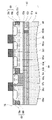
- FIG. 3 is a cross-sectional view schematically showing an example of the device structure of pixels of the imaging device according to the embodiment.
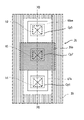
- FIG. 4 is a schematic plan view showing an example layout of each element in a pixel of the imaging device according to the embodiment.
- FIG. 5 is an explanatory diagram illustrating a part of the manufacturing process of the imaging device according to the embodiment.
- FIG. 6 is an explanatory diagram illustrating a part of the manufacturing process of the imaging device according to the embodiment.
- FIG. 7 is an explanatory diagram illustrating a part of the manufacturing process of the imaging device according to the embodiment.
- FIG. 8 is an explanatory diagram illustrating a part of the manufacturing process of the imaging device according to the embodiment.
- FIG. 9 is an explanatory diagram illustrating a part of the manufacturing process of the imaging device according to the embodiment.
- FIG. 10A is an enlarged layout diagram of the vicinity of the reset transistor in the embodiment.
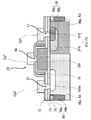
- FIG. 10B is an enlarged cross-sectional view of the vicinity of the reset transistor in the embodiment.
- FIG. 11A is a layout diagram enlarging the vicinity of the charge accumulation region in the embodiment.
- FIG. 11B is a layout diagram illustrating the positional relationship among the first contact holes, PN junctions, element isolation regions, and second contact holes in the embodiment.
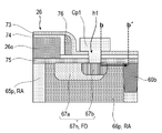
- 12A is a cross-sectional view of the vicinity of a reset transistor in the embodiment; FIG. FIG.
- FIG. 12B is a diagram showing impurity concentration distribution in a direction perpendicular to the surface of the semiconductor substrate in the embodiment.
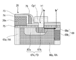
- FIG. 13A is a cross-sectional view of the vicinity of the reset transistor in the reference embodiment.
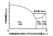
- FIG. 13B is a diagram showing the impurity concentration distribution in the direction parallel to the surface of the semiconductor substrate in the reference embodiment.
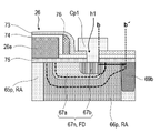
- 14A is a cross-sectional view of the vicinity of a reset transistor in the embodiment;
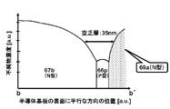
- FIG. 14B is a diagram showing distribution of impurity concentration in a direction parallel to the surface of the semiconductor substrate in the embodiment.
- FIG. FIG. 15A is a cross-sectional view showing distribution of a depletion layer near a reset transistor in the reference embodiment.
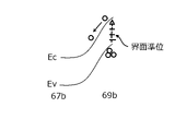
- FIG. 15B is an energy level diagram of the charge storage region and the element isolation region in the reference embodiment.
- FIG. 16A is a cross-sectional view showing distribution of a depletion layer near a reset transistor in the embodiment.
- 16B is an energy level diagram of a charge storage region and an element isolation region according to the embodiment;
- FIG. 17 is a graph showing the results of Experiment A.
- An imaging device includes a semiconductor substrate including a reference region, first impurity regions, second impurity regions, element isolation regions, and specific regions.
- the reference region includes impurities of a first conductivity type.
- Each of the first impurity region and the second impurity region is located within the reference region and includes impurities of a second conductivity type.
- the element isolation region is located between the first impurity region and the second impurity region in plan view and contains the first conductivity type impurity.
- the specific region is located between the surface and the element isolation region in a vertical direction perpendicular to the surface of the semiconductor substrate, and contains the second conductivity type impurity.
- the technique according to the first aspect is suitable for suppressing leakage current between the first impurity region and the second impurity region.
- the first impurity region may be a charge accumulation region that accumulates charges generated by photoelectric conversion.
- the charge accumulation region is an example of the first impurity region.
- the imaging device according to the first or second aspect may further include a transistor having a source and a drain,
- the second impurity region may be one of the source and the drain.
- One of the source and drain of the transistor is an example of the second impurity region.
- a concentration of the second conductivity type impurity at a first point belonging to the specific region may be higher than a concentration of the first conductivity type impurity at a second point belonging to the element isolation region,
- An imaginary straight line passing through the first point and the second point may be perpendicular to the surface.
- the technology according to the fourth aspect is suitable for suppressing leakage current between the first impurity region and the second impurity region.
- the specific region may have a portion where the impurity concentration of the second conductivity type is 1 ⁇ 10 19 cm ⁇ 3 or more.
- the technique according to the fifth aspect is suitable for suppressing leakage current between the first impurity region and the second impurity region.
- the concentration of the second conductivity type impurity at a third point belonging to the specific region may be higher than the concentration of the first conductivity type impurity at a fourth point belonging to the reference region, A virtual straight line passing through the third point, the fourth point, and the fifth point belonging to the first impurity region in this order may be parallel to the surface.
- the technique according to the sixth aspect is suitable for suppressing leakage current between the first impurity region and the second impurity region.
- the concentration of the second conductivity type impurity at a fifth point belonging to the first impurity region may be higher than the concentration of the first conductivity type impurity at a fourth point belonging to the reference region, A virtual straight line passing through the third point, the fourth point, and the fifth point belonging to the specific region in this order may be parallel to the surface.
- the technique according to the seventh aspect is suitable for suppressing leakage current between the first impurity region and the second impurity region.
- the imaging device may further include an insulating layer disposed on the surface, The specific region may be in contact with the insulating layer.
- the configuration of the eighth aspect is one configuration example.
- the imaging device may further include a first contact plug containing a predetermined impurity of the second conductivity type,
- the first impurity region may include a predetermined region,
- the predetermined region may be connected to the first contact plug and contain the predetermined impurity as the impurity of the second conductivity type.
- the technique according to the ninth aspect is suitable for suppressing leakage current between the first impurity region and the second impurity region.
- the imaging device may further include a first contact hole, a second contact plug, and a second contact hole
- the first contact plug may be connected to the predetermined region through the first contact hole
- the second contact plug may be connected to the second impurity region through the second contact hole
- a PN junction may be configured between the predetermined region and the reference region, In plan view, the first contact hole, the PN junction, the isolation region, and the second contact hole may be arranged in this order on a straight line.
- the technique according to the tenth aspect is suitable for suppressing leakage current between the first impurity region and the second impurity region.
- the specific region may contain phosphorus as the impurity of the second conductivity type.
- the technique according to the eleventh aspect is suitable for suppressing leakage current between the first impurity region and the second impurity region.
- the imaging device may further include a first contact plug and a first contact hole,
- the first contact plug may be connected to the first impurity region through the first contact hole,
- a distance between an end of the first contact hole and an end of the specific region may be 50 nm or more and 500 nm or less.
- the technique according to the twelfth aspect is suitable for suppressing leakage current between the first impurity region and the second impurity region.
- the imaging device includes a pixel region in which at least one pixel is provided, and a peripheral circuit that controls the at least one pixel.
- the pixel region may include the first impurity region, the second impurity region, the element isolation region and the specific region,
- the element isolation region may be an implantation isolation region,
- the peripheral region may include shallow trench isolation (STI).
- the configuration according to the thirteenth aspect is one configuration example.
- the reference region may be arranged between the second impurity region and the specific region.
- the fourteenth aspect is advantageous from the viewpoint of avoiding conduction between the second impurity region and the specific region.
- planar view means when viewed from a direction perpendicular to the semiconductor substrate.
- an n-type impurity region having a high concentration of n-type impurities may be referred to as an n + -type impurity region.
- ordinal numbers such as first, second, third... may be used. If an element is given an ordinal, it is not essential that there be a lower numbered element of the same kind. You can change the number of the ordinal nouns as needed.
- the adjustment of each element associated with the difference in the sign of the signal charge can be performed as appropriate.
- the terminology associated with the difference in the positive and negative sign of the signal charge can be appropriately read.
- FIG. 1 (Embodiment 1) The structure and function of the imaging device according to the first embodiment will be described with reference to FIGS. 1 to 4.
- FIG. 1 (Embodiment 1) The structure and function of the imaging device according to the first embodiment will be described with reference to FIGS. 1 to 4.
- FIG. 1 (Embodiment 1) The structure and function of the imaging device according to the first embodiment will be described with reference to FIGS. 1 to 4.
- FIG. 1 is a block diagram showing an exemplary configuration of imaging device 100 according to Embodiment 1 of the present disclosure.
- the imaging device 100 shown in FIG. 1 has a plurality of pixels 10 and peripheral circuits 40 .
- a plurality of pixels 10 and peripheral circuits 40 are provided using a semiconductor substrate 60 .
- the semiconductor substrate 60 is a silicon substrate.
- the pixel 10 has a photoelectric conversion unit 12 .
- the photoelectric conversion unit 12 converts light into electric charges.
- pixels 10 are arranged in a plurality of rows and columns of m rows and n columns.
- m and n independently represent an integer of 1 or more.
- the pixels 10 constitute an imaging region R1 by being arranged two-dimensionally on the semiconductor substrate 60, for example.
- the imaging region R1 is also called a pixel region.
- the number and arrangement of pixels 10 are not limited to the illustrated example.
- the center of each pixel 10 is positioned on a lattice point of a square lattice.
- the center of each pixel 10 may be positioned on a lattice point of a triangular lattice or a hexagonal lattice.
- the pixels 10 may be arranged in one dimension.
- the imaging device 100 can be used as a line sensor.
- the number of pixels 10 included in the imaging device 100 may be one.
- the peripheral circuit 40 includes a vertical scanning circuit 42 and a horizontal signal readout circuit 44. As illustrated in FIG. 1, peripheral circuitry 40 may additionally include control circuitry 46 . Also, the peripheral circuit 40 may further include, for example, a voltage supply circuit that supplies a predetermined voltage to the pixels 10 and the like. Peripheral circuitry 40 may further include signal processing circuitry or output circuitry.
- the peripheral circuit 40 is provided, for example, in a peripheral region R2 positioned around the imaging region R1. In the example shown in FIG. 1, it is an L-shaped area along two sides of the imaging area R1. However, the peripheral region R2 may be an annular region surrounding the imaging region R1. The peripheral region R2 may be an elongated region along one side of the imaging region R1.
- An address signal line 34 is provided for each row of a plurality of pixels 10 . These address signal lines 34 are connected to the vertical scanning circuit 42 .
- the vertical scanning circuit 42 is also called a row scanning circuit. Another signal line may be provided for each row, and these signal lines may be connected to the vertical scanning circuit 42 . In other words, a plurality of types of signal lines may be provided for each row and these signal lines may be connected to the vertical scanning circuit 42 .
- a vertical signal line 35 is provided for each column of a plurality of pixels 10 . These vertical signal lines 35 are connected to a horizontal signal readout circuit 44 .
- the horizontal signal readout circuit 44 is also called a column scanning circuit.
- the control circuit 46 receives command data and a clock, for example, and controls the imaging device 100 as a whole.
- the command data and clock are given from the outside of the imaging device 100, for example.
- control circuit 46 has a timing generator.
- the control circuit 46 can supply drive signals to the vertical scanning circuit 42 and the horizontal signal readout circuit 44 .
- Arrows extending from the control circuit 46 in FIG. 1 schematically represent the flow of output signals from the control circuit 46 .
- Control circuitry 46 may be implemented by a microcontroller, including, for example, one or more processors.
- the functions of the control circuit 46 may be realized by a combination of a general-purpose processing circuit and software, or by hardware specialized for such processing.
- FIG. 2 is a schematic diagram showing an exemplary circuit configuration of the imaging device 100 according to Embodiment 1 of the present disclosure.
- four pixels 10A arranged in two rows and two columns are representatively shown in order to avoid complicating the drawing.
- Each of these pixels 10A is an example of the pixel 10 shown in FIG.
- the pixel 10A has a photoelectric conversion structure 12A and a signal detection circuit 14A.
- the photoelectric conversion structure 12A is provided as the photoelectric conversion section 12 .
- the signal detection circuit 14A is electrically connected to the photoelectric conversion structure 12A.
- Photovoltaic structure 12A includes a photovoltaic layer disposed above semiconductor substrate 60, as will be described later in detail with reference to the drawings. That is, here, a stacked imaging device is exemplified as the imaging device 100 .
- the photoelectric conversion unit 12 may be a photodiode provided in the semiconductor substrate.
- the photoelectric conversion structure 12A of each pixel 10A is connected to the accumulation control line 31.
- a predetermined voltage is applied to the accumulation control line 31 during operation of the imaging apparatus 100 .
- a positive voltage of about 10 V is applied to the accumulation control line 31 during operation of the imaging device 100 .
- sell. A case in which holes are used as signal charges will be exemplified below.
- the signal detection circuit 14A includes a signal detection transistor 22, an address transistor 24 and a reset transistor 26.
- Signal detection transistor 22, address transistor 24 and reset transistor 26 are typically field effect transistors provided in a semiconductor substrate 60 that supports photoelectric conversion structure 12A, as will be described in greater detail below with reference to the drawings. .
- MOSFET Metal Oxide Semiconductor Field Effect Transistor
- the transistors are N-channel MOSFETs.
- the gate electrode of the signal detection transistor 22 is electrically connected to the photoelectric conversion structure 12A.
- the accumulation control line 31 By applying a predetermined voltage to the accumulation control line 31 during operation, holes, for example, can be accumulated as signal charges in the charge accumulation region FD.
- the charge storage region FD is an impurity region provided in the semiconductor substrate 60 .
- the charge storage region FD stores charge generated by the photoelectric conversion structure 12A.
- the imaging device 100 may have a portion that temporarily holds the charges generated by the photoelectric conversion structure 12A. Such portions include, for example, the pixel electrode 12a, the conductive structure 89, the gate electrode of the signal detection transistor 22, and the like.
- One of the source and drain of the signal detection transistor 22 is connected to the power supply wiring 32 .
- the power supply wiring 32 supplies the power supply voltage VDD to each pixel 10A during operation of the imaging device 100 .
- the power supply voltage VDD is, for example, 3.3V.
- the other of the source and drain of the signal detection transistor 22 is connected to the vertical signal line 35 via the address transistor 24 .
- the signal detection transistor 22 outputs a signal voltage corresponding to the amount of signal charge accumulated in the charge accumulation region FD by receiving supply of the power supply voltage VDD at one of its source and drain.
- An address signal line 34 is connected to the gate electrode of the address transistor 24 connected between the signal detection transistor 22 and the vertical signal line 35 .
- the vertical scanning circuit 42 applies a row selection signal for controlling ON/OFF of the address transistor 24 to the address signal line 34 , thereby transmitting the output of the signal detection transistor 22 of the selected pixel 10 A to the corresponding vertical signal line 35 . can be read. Note that the arrangement of the address transistor 24 is not limited to the example shown in FIG.
- a load circuit 45 and a column signal processing circuit 47 are connected to each of the vertical signal lines 35 .
- Load circuit 45 forms a source follower circuit together with signal detection transistor 22 .
- the column signal processing circuit 47 is also called a row signal storage circuit.
- the column signal processing circuit 47 performs, for example, noise suppression signal processing and analog-to-digital conversion. Noise-suppressed signal processing is, for example, correlated double sampling.
- the horizontal signal readout circuit 44 sequentially reads signals from the plurality of column signal processing circuits 47 to the horizontal common signal line 49 .
- Load circuit 45 and column signal processing circuit 47 may be part of peripheral circuit 40 .
- a reset signal line 36 is connected to the gate electrode of the reset transistor 26 .
- the reset signal line 36 is connected to the vertical scanning circuit 42 .
- the reset signal line 36 is provided for each row of the plurality of pixels 10A, similarly to the address signal line 34 .
- the vertical scanning circuit 42 can select the pixels 10A to be reset on a row-by-row basis.
- the vertical scanning circuit 42 can switch on and off the reset transistors 26 in the selected row by applying a reset signal to the gates of the reset transistors 26 via the reset signal line 36 .
- the potential of the charge storage region FD is reset by turning on the reset transistor 26 .
- one of the source and drain of the reset transistor 26 is the charge storage region FD.
- a feedback line 53 is provided for each column of the plurality of pixels 10A. Feedback line 53 is associated with reset transistor 26 . The other of the source and drain of reset transistor 26 is connected to the corresponding feedback line 53 .
- the voltage of the feedback line 53 is supplied to the charge accumulation region FD as the reset voltage for initializing the charge of the photoelectric conversion unit 12 .
- the imaging device 100 has a feedback circuit 16A.
- a feedback path including an inverting amplifier 50 is formed by the feedback circuit 16A.
- the inverting amplifier 50 is provided for each column of the plurality of pixels 10A.
- Feedback line 53 is also associated with inverting amplifier 50 .
- the feedback lines 53 are connected to corresponding output terminals of the inverting amplifiers 50 .
- Inverting amplifier 50 may be part of peripheral circuit 40 .
- the inverting input terminal of the inverting amplifier 50 is connected to the vertical signal line 35 of the corresponding column.
- a non-inverting input terminal of the inverting amplifier 50 is supplied with a reference voltage Vref during operation of the imaging device 100 .
- Vref a reference voltage
- the formation of the feedback path resets the voltage of the charge accumulation region FD to a voltage that makes the voltage of the vertical signal line 35 equal to the reference voltage Vref.
- the reference voltage Vref any voltage within the range of the power supply voltage and ground can be used.
- the reference voltage Vref is, for example, a positive voltage of 1V or around 1V.
- FIG. 3 Details of the device structure of the pixel 10A will be explained using FIGS. 3 and 4.
- FIG. 3 Details of the device structure of the pixel 10A will be explained using FIGS. 3 and 4.
- FIG. 3 is a cross-sectional view schematically showing an example of the device structure of the pixel 10A of the imaging device 100 according to Embodiment 1 of the present disclosure.
- FIG. 4 is a schematic plan view showing an example layout of each element in the pixel 10A of the imaging device 100 according to the present embodiment. 4 schematically shows the arrangement of elements formed on the semiconductor substrate 60 when the pixel 10A shown in FIG. 3 is viewed along the normal direction of the semiconductor substrate 60. FIG. If the pixel 10A is cut along the line III-III in FIG. 4 and expanded, the cross section shown in FIG. 3 is obtained.
- the insulating layer 75 and the like are omitted.
- Pixel 10A includes semiconductor substrate 60, photoelectric conversion structure 12A and conductive structure 89.
- FIG. As shown, photoelectric conversion structure 12A is disposed above semiconductor substrate 60 . Specifically, photoelectric conversion structure 12A is supported by interlayer insulating layer 90 covering semiconductor substrate 60 . Conductive structure 89 is disposed within interlayer insulating layer 90 .
- the interlayer insulating layer 90 includes multiple insulating layers.
- the multiple insulating layers include a seventh insulating layer 91 .
- the seventh insulating layer 91 is also called a pre-metal insulating film (Pre-Metal-Dielectric).
- Conductive structure 89 includes via plug 88 .
- the conductive structure 89 also includes a portion of each of the multiple wiring layers. The part is arranged inside the interlayer insulating layer 90 .
- via plug 88 is a metal plug. The via plug 88 is accommodated in the connection hole 88h.
- a plurality of wiring layers arranged in the interlayer insulating layer 90 has at least one of, for example, the address signal line 34, the reset signal line 36, the vertical signal line 35, the power supply wiring 32, and the feedback line 53 as part thereof. Wiring layers may be included.
- the number of insulating layers and the number of wiring layers in the interlayer insulating layer 90 are not limited to this example. The number of insulating layers and the number of wiring layers can be set arbitrarily.
- Metal wiring 87 may be used.
- Metal traces 87 are traces included in conductive structure 89 .
- the metal wiring 87 can correspond to a part of, for example, the address signal line 34, the reset signal line 36, the vertical signal line 35, the power supply wiring 32, the feedback line 53, and the like.
- the photoelectric conversion structure 12A includes a pixel electrode 12a, a counter electrode 12c and a photoelectric conversion layer 12b.
- the photoelectric conversion layer 12b is arranged between the pixel electrode 12a and the counter electrode 12c.
- the pixel electrode 12 a is provided on the interlayer insulating layer 90 .
- the counter electrode 12c is arranged on the light incident side.
- the material of the photoelectric conversion layer 12b may be an organic material or an inorganic material.
- An inorganic material is, for example, amorphous silicon.
- the photoelectric conversion layer 12b receives light incident through the counter electrode 12c and generates positive and negative charges through photoelectric conversion.
- the photoelectric conversion layer 12b is typically provided continuously over a plurality of pixels 10A.
- the photoelectric conversion layer 12b may include a layer made of an organic material and a layer made of an inorganic material.
- the photoelectric conversion layer 12b may be provided separately for each pixel 10A.
- the counter electrode 12c is a translucent electrode made of a transparent conductive material.
- the transparent conductive material is, for example, ITO (Indium Tin Oxide).
- the term “translucent” in the present embodiment means that at least part of light having a wavelength that can be absorbed by the photoelectric conversion layer 12b is transmitted. Not required.
- the counter electrode 12c is provided continuously over the plurality of pixels 10A, similar to the photoelectric conversion layer 12b. In other words, the common electrode 12c is shared by a plurality of pixels 10A.
- the counter electrode 12c may be provided separately for each pixel 10A.
- the counter electrode 12c is connected to the accumulation control line 31.
- the potential of the storage control line 31 is controlled to make the potential of the counter electrode 12c higher than the potential of the pixel electrode 12a. This allows the pixel electrodes 12a to selectively collect the positive charges out of the positive and negative charges generated by photoelectric conversion.
- a predetermined potential can be applied collectively to the counter electrodes 12c of the plurality of pixels 10A.
- the material of the pixel electrode 12a is, for example, metal, metal nitride, or the like.
- the material of the pixel electrode 12a may be polysilicon to which conductivity is imparted by being doped with impurities. Examples of metals include aluminum and copper.
- the pixel electrode 12a is spatially separated from the pixel electrode 12a of the adjacent pixel 10A, thereby being electrically separated from the pixel electrode 12a of the other pixel 10A.
- the conductive structure 89 includes multiple wires and plugs. One end of the conductive structure 89 is connected to the pixel electrode 12a. The other end of the conductive structure 89 is connected to the charge storage region FD. In the illustrated example, the charge storage region FD is the n-type impurity region 67n.
- Materials for the plurality of wirings and plugs are, for example, metals, metal compounds, and the like. Examples of metals include copper and tungsten. Examples of metal compounds include metal nitrides and metal oxides. The material of the plurality of wires and plugs may be polysilicon to which conductivity is imparted.
- the semiconductor substrate 60 includes a support substrate 61 and one or more semiconductor layers provided on the support substrate 61 .
- a p-type silicon substrate is exemplified as the support substrate 61 .
- the semiconductor substrate 60 has a p-type semiconductor layer 61p, an n-type semiconductor layer 62n, a p-type semiconductor layer 63p and a p-type semiconductor layer 65p.
- a p-type semiconductor layer 61p is located on the support substrate 61 .
- An n-type semiconductor layer 62n is located on the p-type semiconductor layer 61p.
- a p-type semiconductor layer 63p is located on the n-type semiconductor layer 62n.
- a p-type semiconductor layer 65p is located on the p-type semiconductor layer 63p.
- the p-type semiconductor layer 63p is provided over the entire surface of the support substrate 61.
- Each of the n-type semiconductor layer 62n, the p-type semiconductor layer 63p, and the p-type semiconductor layer 65p is typically formed by ion implantation of impurities into semiconductor layers formed by epitaxial growth.
- the impurity concentration in the p-type semiconductor layer 63p and the p-type semiconductor layer 65p is higher than the impurity concentration in the p-type semiconductor layer 61p.
- the impurity concentration of the p-type semiconductor layer 63p is higher than that of the p-type semiconductor layer 65p.
- the impurity concentration of the p-type semiconductor layer 61p is, for example, approximately 10 15 cm ⁇ 3
- the impurity concentration of the p-type semiconductor layer 65p is, for example, approximately 10 17 cm ⁇ 3
- the impurity concentration of the p-type semiconductor layer 63p can be, for example, approximately 10 17 cm ⁇ 3 to 10 18 cm ⁇ 3 .
- the mutual relationship between the impurity concentrations described above is merely an example, and a configuration in which the impurity concentrations in the p-type semiconductor layer 63p and the p-type semiconductor layer 65p are approximately the same may be adopted.
- the impurity concentration in the p-type semiconductor layer 65p may exceed the impurity concentration in the p-type semiconductor layer 63p.
- the n-type semiconductor layer 62n is located between the p-type semiconductor layer 61p and the p-type semiconductor layer 63p. Although not shown in FIG. 3, a well contact is connected to the n-type semiconductor layer 62n. A well contact is provided outside the imaging region R1, and the potential of the n-type semiconductor layer 62n is controlled via the well contact during operation of the imaging device 100. FIG. By providing the n-type semiconductor layer 62n, the inflow of minority carriers from the support substrate 61 or the peripheral circuit 40 into the charge storage region FD that stores signal charges is suppressed.
- the semiconductor substrate 60 has a p-type region 64 .
- the p-type region 64 is provided between the p-type semiconductor layer 63p and the support substrate 61 so as to penetrate the p-type semiconductor layer 61p and the n-type semiconductor layer 62n.
- the p-type region 64 has a higher impurity concentration than the p-type semiconductor layer 63p and the p-type semiconductor layer 65p.
- the p-type region 64 electrically connects the p-type semiconductor layer 63p and the support substrate 61 .
- the support substrate 61 is connected to substrate contacts provided outside the imaging region R1. During operation of the imaging device 100, the potentials of the supporting substrate 61 and the p-type semiconductor layer 63p are controlled via the substrate contacts. Further, by arranging the p-type semiconductor layer 65p so as to be in contact with the p-type semiconductor layer 63p, it is possible to control the potential of the p-type semiconductor layer 65p through the p-type semiconductor layer 63p during operation of the imaging device 100. be. Note that the p-type semiconductor layer 65p is provided as a p-well.
- the p-type impurity layer 66p is located within the p-type semiconductor layer 65p.
- the impurity concentration of the p-type impurity layer 66p is lower than that of the p-type semiconductor layer 65p.
- n-type impurity region 67n is an example of the charge storage region FD.
- n-type impurity region 67n is located in p-type semiconductor layer 66p.
- n-type impurity region 67n is located near the surface of semiconductor substrate 60 . At least part of n-type impurity region 67n is in contact with the surface of semiconductor substrate 60 .
- the n-type impurity region 67n includes a first region 67a and a second region 67b.
- the impurity concentration of the second region 67b is higher than that of the first region 67a.
- the second region 67b is an n + -type impurity region.
- the p-type semiconductor layer 66p is provided as a p-well.
- a junction capacitance formed by a PN junction between the p-type semiconductor layer 66p and the n-type impurity region 67n functions as a capacitance that stores at least part of the signal charge.
- the n-type impurity region 67n functions as a charge accumulation region FD that temporarily holds signal charges.
- the potential of the p-type semiconductor layer 65p can be controlled via the p-type semiconductor layer 63p during operation of the imaging device 100. is possible.
- the first region 67a and the p-type semiconductor layer 66p can be arranged around the second region 67b.
- the first region 67a and the p-type semiconductor layer 66p extend on the p-type semiconductor layer 63p side and the gate electrode 26e side of the reset transistor when viewed from the second region 67b.
- the PN junction between the n-type impurity region 67n and the p-type semiconductor layer 66p on these sides is the PN junction between the first region 67a and the p-type semiconductor layer 66p.
- the impurity concentration of the first region 67a is lower than that of the second region 67b, and the impurity concentration of the p-type semiconductor layer 66p is lower than that of the p-type semiconductor layer 65p. Since the PN junction is configured using the first region 67a and the p-type semiconductor layer 66p, the electric field intensity generated by the PN junction can be relaxed. Therefore, leakage current caused by the electric field can be suppressed.
- the p-type semiconductor layer 66p extends on the blocking structure 69 side when viewed from the second region 67b.
- the PN junction between the n-type impurity region 67n and the p-type semiconductor layer 66p on this side is the PN junction between the second region 67b and the p-type semiconductor layer 66p.
- the second region 67b has a higher impurity concentration than the first region 67a
- the p-type semiconductor layer 66p has a lower impurity concentration than the p-type semiconductor layer 65p. Since the PN junction is formed using such p-type semiconductor layer 66p, the electric field intensity formed by the PN junction can be relaxed. Therefore, leakage current caused by the electric field can be suppressed.
- the n-type impurity region 68an, the n-type impurity region 68bn, the n-type impurity region 68cn, and the n-type impurity region 68dn are located within the p-type semiconductor layer 65p.
- the n-type impurity region 68an also includes a first region having a relatively low impurity concentration and a second region having a relatively high impurity concentration.
- the second region is an n+ type impurity region.
- a blocking structure 69 is located between the p-type semiconductor layer 65p and the p-type semiconductor layer 66p.
- the blocking structure 69 has a specific region 69a and an isolation region 69b.
- the specific region 69a and the element isolation region 69b are stacked on each other.
- a PN junction is formed between the specific region 69a and the element isolation region 69b.
- the specific region 69a is positioned closer to the front surface of the semiconductor substrate 60 than the element isolation region 69b.
- the element isolation region 69b is positioned closer to the support substrate 61 than the specific region 69a.
- the specific region 69a is an n-type impurity region. Specifically, the specific region 69a is an n + -type impurity region.
- the element isolation region 69b is a p-type semiconductor layer. In the example of FIG. 3, the element isolation region 69b is an implantation isolation region formed by ion implantation.
- FIG. 3 three blocking structures 69 are shown.
- One blocking structure 69 is located between the n-type impurity region 68an and the edge of the pixel 10A.
- Another blocking structure 69 is positioned between the charge accumulation region FD and the n-type impurity region 68bn within the same pixel 10A.
- Yet another blocking structure 69 is located between the n-type impurity region 68dn and another edge of the pixel 10A.
- a p-type semiconductor layer 65p is arranged between the n-type impurity region 68an and the blocking structure 69 in plan view. In this way, it is easy to prevent the n-type impurity region 68an from being electrically connected to the specific region 69a of the blocking structure 69, which is also n-type. This is advantageous from the viewpoint of normal operation of the reset transistor 26 .
- a portion of the p-type semiconductor layer 65p between the n-type impurity region 68an and the blocking structure 69 is defined as a first p-type semiconductor portion.
- a p-type semiconductor layer 65p is arranged between the n-type impurity region 68bn and the blocking structure 69 in plan view. In this way, it is easy to prevent the n-type impurity region 68bn from being electrically connected to the specific region 69a of the blocking structure 69, which is also n-type. This is advantageous from the viewpoint of normal operation of the signal detection transistor 22 .
- a portion of the p-type semiconductor layer 65p between the n-type impurity region 68bn and the blocking structure 69 is defined as a second p-type semiconductor portion.
- a p-type semiconductor layer 65p is arranged between the n-type impurity region 68cn and the blocking structure 69 in plan view. In this way, it is easy to prevent the n-type impurity region 68cn from being electrically connected to the specific region 69a of the blocking structure 69, which is also n-type. This is advantageous from the viewpoint of normal operation of the signal detection transistor 22 and the address transistor 24 .
- a portion of the p-type semiconductor layer 65p between the n-type impurity region 68cn and the blocking structure 69 is defined as a third p-type semiconductor portion.
- a p-type semiconductor layer 65p is arranged between the n-type impurity region 68dn and the blocking structure 69 in plan view. In this way, it is easy to prevent the n-type impurity region 68dn from conducting with the specific region 69a of the blocking structure 69, which is also n-type. This is advantageous from the viewpoint of normal operation of the address transistor 24 .
- a portion of the p-type semiconductor layer 65p between the n-type impurity region 68dn and the blocking structure 69 is defined as a fourth p-type semiconductor portion.
- the contact plug Cp1 is connected through the third insulating layer 73, the fourth insulating layer 74 and the fifth insulating layer 75 to the second region 67b, which is the n-type impurity region.
- the contact plug Cp2 is connected to the n-type impurity region 68bn via the third insulating layer 73, the fourth insulating layer 74 and the fifth insulating layer 75.
- the contact plug Cp3 is connected to the n-type impurity region 68an via the third insulating layer 73, the fourth insulating layer 74 and the fifth insulating layer 75. As shown in FIG.
- the contact plug Cp4 is connected to the n-type impurity region 68dn through the third insulating layer 73, the fourth insulating layer 74 and the fifth insulating layer 75. As shown in FIG. The contact plug Cp5 is connected through the third insulating layer 73 and the fourth insulating layer 74 to the gate electrode 22e. The contact plug Cp6 is connected through the third insulating layer 73 and the fourth insulating layer 74 to the gate electrode 24e. The contact plug Cp7 is connected through the third insulating layer 73 and the fourth insulating layer 74 to the gate electrode 26e.
- the contact plugs Cp1 to Cp7 contain highly doped impurities.
- the impurity is phosphorus.
- the high impurity concentration of the second region 67b of the n-type impurity region 67n is realized by impurity diffusion from the contact plug Cp1.
- high impurity concentrations in the second regions of the n-type impurity regions 68an, 68bn and 68dn are achieved by diffusion of impurities from the contact plugs Cp3, Cp2 and Cp4, respectively.
- range Rp and peak concentration are used as indicators of ion implantation.
- the range Rp is the ion implantation depth.
- the range Rp means the depth at which the peak value of the impurity concentration is obtained.
- a p-type semiconductor layer 61p, an n-type semiconductor layer 62n, and a p-type semiconductor layer 63p are formed by ion implantation of impurities into semiconductor layers formed by epitaxial growth.
- the p-type impurity implanted into the p-type semiconductor layer 61p is boron.
- the impurity concentration in the p-type semiconductor layer 61p is approximately 1 ⁇ 10 15 cm ⁇ 3 to 5 ⁇ 10 15 cm ⁇ 3 .
- the n-type impurity implanted into the n-type semiconductor layer 62n is phosphorus.
- the range Rp of impurities in the n-type semiconductor layer 62n from the surface of the semiconductor substrate 60 is 1300 nm to 1600 nm.
- the peak impurity concentration in the n-type semiconductor layer 62n is about 2 ⁇ 10 16 cm ⁇ 3 to 8 ⁇ 10 16 cm ⁇ 3 .
- the p-type impurity implanted into the p-type semiconductor layer 63p is boron.
- the range Rp of impurities in the p-type semiconductor layer 63p from the surface of the semiconductor substrate 60 is 800 nm to 1000 nm.
- the peak impurity concentration in the p-type semiconductor layer 63p is about 1 ⁇ 10 17 cm ⁇ 3 to 5 ⁇ 10 17 cm ⁇ 3 .
- "x" means multiplication.
- p-type region 64 is formed by photolithography and ion implantation.
- the thickness of the resist film used for photolithography is about 4 ⁇ m to 5 ⁇ m.
- the pattern size to be formed is about 500 to 1000 nm.
- Ion implantation is done in multiple stages. Specifically, ion implantation is performed in two stages.
- the implanted p-type impurity is boron.
- the range Rp of impurities from the surface of the semiconductor substrate 60 is 1100 nm to 1400 nm.
- the peak concentration of impurities in the p-type region 64 resulting from the first-stage ion implantation is about 1 ⁇ 10 17 cm ⁇ 3 to 5 ⁇ 10 17 cm ⁇ 3 .
- the range Rp of impurities from the surface of the semiconductor substrate 60 is 1300 nm to 1600 nm.
- the peak concentration of impurities in the p-type region 64 resulting from the second-stage ion implantation is about 3 ⁇ 10 17 cm ⁇ 3 to 9 ⁇ 10 17 cm ⁇ 3 .
- the p-type semiconductor layer 65p is formed by photolithography and ion implantation.
- a region corresponding to the p-type semiconductor layer 66p is covered with a resist by photolithography.
- an opening is formed by removing the resist. Since ion implantation is performed in this state, ion implantation is not performed in the region corresponding to p-type semiconductor layer 66p, but ion implantation is performed in the region corresponding to p-type semiconductor layer 65p.
- Ion implantation is done in multiple stages. Ion implantation is specifically performed in two stages. The implanted p-type impurity is boron.
- the range Rp of impurities from the surface of the semiconductor substrate 60 is 300 nm to 500 nm.
- the peak concentration of impurities in the p-type semiconductor layer 65p resulting from the first-stage ion implantation is about 7 ⁇ 10 16 cm ⁇ 3 to 2 ⁇ 10 17 cm ⁇ 3 .
- the range Rp of impurities from the surface of the semiconductor substrate 60 is 500 nm to 700 nm.
- the peak concentration of impurities in the p-type semiconductor layer 65p resulting from the second-stage ion implantation is about 1 ⁇ 10 16 cm ⁇ 3 to 5 ⁇ 10 16 cm ⁇ 3 .
- the first region 67a of the n-type impurity region 67n is formed by photolithography and ion implantation.
- the implanted n-type impurity is arsenic.
- the range Rp of impurities from the surface of the semiconductor substrate 60 is 50 nm to 100 nm.
- the peak impurity concentration in the first region 67a of the n-type impurity region 67n is about 1 ⁇ 10 17 cm ⁇ 3 to 5 ⁇ 10 17 cm ⁇ 3 .
- the n-type impurity region 67n is one of the source and drain of the reset transistor 26.
- the fifth insulating layer 75 is formed by, for example, the ISSG (In Situ Steam Generation) method.
- the fifth insulating layer 75 is a gate oxide film.
- the thickness of the fifth insulating layer 75 is about 7 nm to 10 nm.
- the gate electrode 22e, the gate electrode 24e and the gate electrode 26e are formed on the fifth insulating layer 75. These electrodes 22e, 24e and 26e are formed using a polysilicon material. This polysilicon material contains a high concentration of n-type impurities derived from ion implantation. A film of the polysilicon material is formed on the fifth insulating layer 75 with a thickness of about 100 nm to 200 nm. This film is processed by photolithography and dry etching. Thus, gate electrodes 22e, 24e and 26e are formed. The gate electrodes 22e, 24e and 26e are imparted with electrical conductivity by being made low in resistance by the n-type impurity.
- the specific region 69a and the element isolation region 69b of the blocking structure 69 are formed by photolithography and ion implantation.
- Ion implantation for the element isolation region 69b is performed in a plurality of stages. This ion implantation is specifically performed in two stages.
- the implanted p-type impurity is boron.
- the range Rp of impurities from the surface of the semiconductor substrate 60 is 20 nm to 50 nm.
- the peak concentration of impurities in the element isolation region 69b resulting from the first-stage ion implantation is about 1 ⁇ 10 18 cm ⁇ 3 to 3 ⁇ 10 18 cm ⁇ 3 .
- the range Rp of impurities from the surface of the semiconductor substrate 60 is 120 nm to 180 nm.
- the peak concentration of impurities in the element isolation region 69b resulting from the second-stage ion implantation is about 3 ⁇ 10 17 cm ⁇ 3 to 6 ⁇ 10 17 cm ⁇ 3 .
- the implanted n-type impurity is phosphorus.
- the range Rp of impurities from the surface of the semiconductor substrate 60 is 2 nm to 10 nm.
- the peak impurity concentration in the specific region 69a is about 1 ⁇ 10 19 cm ⁇ 3 to 5 ⁇ 10 19 cm ⁇ 3 .
- an n-type impurity region 68an, an n-type impurity region 68bn, an n-type impurity region 68cn and an n-type impurity region 68dn are formed by photolithography and ion implantation.
- the implanted n-type impurity is arsenic.
- the range Rp of impurities from the surface of the semiconductor substrate 60 is 10 nm to 30 nm.
- each of the n-type impurity regions 68an, 68bn, 68cn and 68dn is approximately 5 ⁇ 10 19 cm ⁇ 3 to 9 ⁇ 10 19 cm ⁇ 3 .
- each of n-type impurity regions 68an, 68bn, 68cn and 68dn is one of the source and drain of a transistor.
- the order of forming the blocking structure 69, the n-type impurity region 68an, the n-type impurity region 68bn, the n-type impurity region 68cn, and the n-type impurity region 68dn is not particularly limited.
- contact plugs Cp1 to Cp7 contain heavily doped phosphorus.
- the contact plugs Cp1 to Cp7 are formed by processing films obtained by depositing these materials.
- the film contains phosphorous with a concentration of 6 ⁇ 10 20 cm ⁇ 3 to 8 ⁇ 10 20 cm ⁇ 3 as soon as it is deposited.
- heat treatment at 800° C. or higher activates phosphorus in the contact plugs Cp1 to Cp7. Due to this activation, the concentration of phosphorus in the contact plugs Cp1 to Cp7 is reduced from 5 ⁇ 10 20 cm ⁇ 3 to 6 ⁇ 10 20 cm ⁇ 3 by outward diffusion due to heat treatment.
- phosphorus in the contact plugs Cp1, Cp3, Cp2 and Cp4 diffuses into the n-type impurity region 67n, the n-type impurity region 68an, the n-type impurity region 68bn and the n-type impurity region 68dn, respectively, due to heat during heat treatment. .
- second regions having a high impurity concentration are formed in the n-type impurity region 67n, the n-type impurity region 68an, the n-type impurity region 68bn, and the n-type impurity region 68dn.
- the second region is an n+ type impurity region.
- An insulating layer is arranged on the surface of the semiconductor substrate 60 on the photoelectric conversion structure 12A side.
- the surface of the semiconductor substrate 60 on the photoelectric conversion structure 12A side is covered with a first insulating layer 71, a second insulating layer 72, a third insulating layer 73, a fourth insulating layer 74, and a fifth insulating layer 75.
- the fifth insulating layer 75 is a gate insulating layer.
- the fifth insulating layer 75 is typically a gate oxide film.
- the first insulating layer 71, the third insulating layer 73, the fourth insulating layer 74, and the fifth insulating layer 75 each contain silicon oxide.
- the first insulating layer 71, the third insulating layer 73, the fourth insulating layer 74, and the fifth insulating layer 75 each contain silicon dioxide.
- the second insulating layer 72 contains silicon nitride.
- a fourth insulating layer 74 is provided on the fifth insulating layer 75 .
- a gate electrode 22 e , a gate electrode 24 e and a gate electrode 26 e are provided on the fifth insulating layer 75 .
- a sixth insulating layer 76 is provided on the side walls of the gate electrodes 22e, 24e, and 26e with a portion of the fourth insulating layer 74 interposed therebetween.
- the sixth insulating layer 76 is a sidewall spacer.
- the sixth insulating layer 76 is also called a sidewall.
- the sixth insulating layer 76 has a laminated structure including a plurality of insulating layers.
- sixth insulating layer 76 includes a silicon dioxide layer and a silicon nitride layer.
- the fourth insulating layer 74 is an offset sidewall spacer. Offset sidewall spacers are also called offset sidewalls.
- the fourth insulating layer 74 is used to reduce overlap capacitance for improving the circuit speed of the transistor when forming the transistor of the peripheral circuit 40 . Further, the fourth insulating layer 74 is used for improving the short channel of the transistor by heat treatment using a furnace which is a diffusion furnace.
- the third insulating layer 73, the fourth insulating layer 74 and the fifth insulating layer 75 are laminated.
- a contact hole h1, a contact hole h2, a contact hole h3, and a contact hole h4 are provided in the laminated structure of the third insulating layer 73, the fourth insulating layer 74, and the fifth insulating layer 75.
- the contact hole h1 is provided on the n-type impurity region 67n. Specifically, the contact hole h1 is provided on the second region 67b, which is an n + -type impurity region.
- the contact hole h2 is provided on the n-type impurity region 68bn.
- Contact hole h3 is provided on n-type impurity region 68an.
- Contact hole h4 is provided on n-type impurity region 68dn.
- the contact plugs Cp1 to Cp7 are all non-silicide and substantially made of polysilicon. Contact plugs Cp1 to Cp7 contain n-type impurities. In this embodiment, contact plugs Cp1 to Cp7 have non-silicide surfaces. In this embodiment, contact plugs Cp1 to Cp7 contain phosphorus as an impurity.
- silicide is a compound of metal and silicon. Silicon is a concept that includes polysilicon.
- a non-silicide contact plug is substantially free of silicide regions.
- the non-silicided contact plug is composed substantially entirely of silicon in one example, and is composed substantially entirely of polysilicon in one embodiment.
- a non-silicided surface is substantially free of regions of silicide.
- the non-silicided surface is composed substantially entirely of silicon in one example, and is composed substantially entirely of polysilicon in one embodiment.
- substantially free of silicide regions refers to a total silicide content of less than 10% by mass, typically less than 5% by mass. , this content may be zero mass %.
- substantially composed of silicon means that the silicon content of the whole is 90% by mass or more, typically the content is 95% by mass or more, and the content is It may be 100% by mass. The same applies to “consisting substantially of polysilicon”.
- silicide is formed in peripheral region R2.
- the non-silicide surfaces of the contact plugs Cp1 to Cp7 are in contact with the via plugs 88. Further, the non-silicide surfaces of the contact plugs Cp1 to Cp7 are in contact with portions of the first insulating layer 71 located above the contact plugs Cp1 to Cp7.
- the upper side of the contact plug means the opposite side of the semiconductor substrate 60 viewed from the contact plug.
- the contact plug Cp1 connects the conductive structure 89 and the n-type impurity region 67n while passing through the contact hole h1.
- the contact plug Cp1 connects the conductive structure 89 and the second region 67b, which is the n + -type impurity region, while passing through the contact hole h1.
- the n-type impurity region 67n is electrically connected to the pixel electrode 12a of the photoelectric conversion section 12 via the contact plug Cp1 and the conductive structure 89.
- the n-type impurity region 67n is the charge storage region FD. Signal charges generated in the photoelectric conversion unit 12 are accumulated in the n-type impurity region 67n.
- the impurity in the second region 67b is introduced by diffusion from the contact plug Cp1.
- the impurity in the second region 67b is introduced by diffusion from the contact plug Cp1 during heat treatment during manufacturing of the imaging device 100.
- the second region 67b contains impurities having the same composition as the impurities of the contact plug Cp1.
- this impurity is phosphorus.
- the concentration of this impurity in the second region 67b is high. This high impurity concentration reduces contact resistance between n-type impurity region 67n and contact plug Cp1.
- the impurity concentration of the second region 67b is, for example, approximately 5 ⁇ 10 20 cm ⁇ 3 .
- a signal detection circuit 14A is provided on the semiconductor substrate 60 . As described above, the signal detection circuit 14A includes the signal detection transistor 22, the address transistor 24 and the reset transistor 26. FIG.
- the signal detection transistor 22 includes an n-type impurity region 68bn as one of its source and drain.
- the signal detection transistor 22 includes an n-type impurity region 68cn as the other of the source and drain.
- Signal detection transistor 22 further includes a gate electrode 22e.
- the gate electrode 22 e is provided on the fifth insulating layer 75 .
- a portion of the fifth insulating layer 75 located between the gate electrode 22 e and the semiconductor substrate 60 functions as a gate insulating layer of the signal detection transistor 22 .
- the gate electrode 22e is connected to the pixel electrode 12a and the n-type impurity region 67n via the contact plug Cp5 and the conductive structure 89. As shown in FIG.
- the gate electrode 22e is connected to the portion 39 of the conductive structure 89 that connects the pixel electrode 12a and the contact plug Cp5 to each other in the layer where the address signal line 34 and the reset signal line 36 are located.
- a contact plug Cp2 is connected to the n-type impurity region 68bn. A portion of the contact plug Cp2 is provided inside the contact hole h2. A power supply wiring 32 as a source follower power supply is electrically connected to the contact plug Cp2. 3, illustration of the power supply wiring 32 is omitted.
- the address transistor 24 includes an n-type impurity region 68cn as one of its source and drain.
- the address transistor 24 includes an n-type impurity region 68dn as the other of the source and drain.
- Address transistor 24 further includes a gate electrode 24e.
- the gate electrode 24 e is provided on the fifth insulating layer 75 .
- a portion of the fifth insulating layer 75 located between the gate electrode 24 e and the semiconductor substrate 60 functions as a gate insulating layer of the address transistor 24 .
- the address signal line 34 is connected to the gate electrode 24e via the contact plug Cp6 and the conductive structure 89. As shown in FIG. In this example, the address transistor 24 and the signal detection transistor 22 are electrically connected to each other by sharing the n-type impurity region 68cn.
- a contact plug Cp4 is connected to the n-type impurity region 68dn. A portion of the contact plug Cp4 is provided inside the contact hole h4. The contact plug Cp4 is electrically connected to the vertical signal line 35. As shown in FIG.
- the reset transistor 26 includes an n-type impurity region 67n as one of its source and drain.
- the reset transistor 26 includes an n-type impurity region 68an as the other of the source and drain.
- one of the source and drain of the reset transistor 26 is the n-type charge storage region FD.
- Reset transistor 26 further includes a gate electrode 26e.
- the gate electrode 26 e is provided on the fifth insulating layer 75 .
- a portion of the fifth insulating layer 75 located between the gate electrode 26 e and the semiconductor substrate 60 functions as a gate insulating layer of the reset transistor 26 .
- the reset signal line 36 is connected to the gate electrode 26e via the contact plug Cp7 and the conductive structure 89. As shown in FIG.
- the n-type impurity region 68an is connected to the contact plug Cp3, as shown in FIG. A portion of the contact plug Cp3 is provided inside the contact hole h3. Contact plug Cp3 is electrically connected to feedback line 53 via conductive structure 89 .
- the first insulating layer 71 is in contact with the top and side surfaces of the contact plugs Cp1 to Cp7.
- a gate electrode 22e, a contact plug Cp5, and a first insulating layer 71 are stacked in this order.
- a gate electrode 24e, a contact plug Cp6, and a first insulating layer 71 are laminated in this order.
- a gate electrode 26e, a contact plug Cp7, and a first insulating layer 71 are laminated in this order.
- the first insulating layer 71 has the effect of suppressing the diffusion of impurities from the inside of the contact plugs Cp1 to Cp7 to the outside.
- the thickness of the first insulating layer 71 in the imaging device 100 is, for example, 10 nm or more and 15 nm or less. By setting the thickness in this manner, the above effects can be ensured.
- metal is introduced into the peripheral circuit 40 to form silicide.
- metal is introduced not only in the peripheral region R2 but also in the imaging region R1.
- the first insulating film 71 functions as a silicide block that prevents the contact plugs Cp1 to Cp7 of the metal introduced into the imaging region R1 in the silicide formation process. If the thickness of the first insulating layer 71 is 10 nm or more and 15 nm or less, the silicide blocking function can be exhibited. Further, if the thickness of the first insulating layer 71 is within this range, it is possible to reduce the global level difference between the peripheral circuit R2 and the imaging region R1.
- the second insulating layer 72 contains silicon nitride.
- the second insulating layer 72 functions as an etching stopper when the seventh insulating layer 91 is formed.
- the thickness of the second insulating layer 72 is, for example, 30 nm or more and 50 nm or less. If the thickness is within this range, the parasitic capacitance of the second insulating layer 72 can be suppressed while ensuring the function as an etching stopper.
- the seventh insulating layer 91 is part of the interlayer insulating layer 90 .
- the seventh insulating layer 91 contains silicon dioxide.
- the thickness of the seventh insulating layer 91 is, for example, about 300 nm to 600 nm.
- a connection hole 88 h is provided in the seventh insulating layer 91 .
- the connection hole 88h is formed by photolithography and dry etching.
- a conductive metal is embedded in the connection hole 88h. This conductive metal constitutes the via plug 88 .
- a conductive metal is, for example, W (tungsten).
- the via plug 88 is connected to the pixel electrode 12a through the metal wiring 87. As shown in FIG.
- the third insulating layer 73 contains silicon dioxide. When at least a portion of the third insulating film 73 exists between two components, the third insulating layer 73 can ensure dielectric strength between those components.
- Through holes are provided in the portions of the third insulating layer 73, the fourth insulating layer 74, and the fifth insulating layer 75 above the source and drain of the transistor of the signal detection circuit 14A. Some of these through holes correspond to contact holes h1 to h4. Through holes can be formed by photolithography and dry etching. The diameter of the through holes is, for example, 80 to 100 nm.
- a through hole is also provided above the gate electrode of the transistor of the signal detection circuit 14A.
- These through holes can also be formed by photolithography and dry etching.
- a part of the contact plug Cp1 is provided inside the through hole.
- Contact plugs Cp1 to Cp7 can be formed as follows. That is, after forming the through holes, the step of growing phosphorus-doped polysilicon is carried out. As a result, a film of about 100 nm, for example, is deposited. Next, this deposited film is partially removed. Thereby, contact plugs Cp1 to Cp7 are formed.
- the impurities contained in the contact plugs Cp1 to Cp7 are activated by heat treatment.
- the impurity is phosphorus. Since the impurities are activated, the resistance of contact plugs Cp1 to Cp7 is small. This is because the heat treatment causes the impurities to be taken into the crystals inside the polysilicon grain boundaries and to act as carriers easily.
- the heat treatment is performed, for example, using a diffusion furnace at a temperature of 800° C. or higher in a nitrogen atmosphere.
- the heat treatment heats the contact plug Cp1 to a high temperature
- the impurities inside the contact plug Cp1 diffuse into the second region 67b of the n-type impurity region 67n.
- the impurity concentration is increased in a portion of n-type impurity region 67n.
- the region where the impurity concentration is increased in this manner is the second region 67b, which is the n + -type impurity region.
- Similar impurity diffusion occurs between contact plugs Cp2 to Cp4 and n-type impurity regions 68bn, 68an and 68dn connected thereto.
- the heat treatment also has the effect of recovering crystal defects caused by damage during ion implantation and dry etching into the n-type impurity region 67n.
- FIG. 10A is an enlarged layout diagram of the vicinity of the reset transistor 26 in the present embodiment.
- FIG. 10B is an enlarged cross-sectional view of the vicinity of the reset transistor 26 in this embodiment. Specifically, FIG. 10B is a cross-sectional view taken along line XB-XB in FIG. 10A.
- the blocking structure 69 is located apart from the n-type impurity region 67n in plan view. In other words, blocking structure 69 is not in contact with n-type impurity region 67n.
- a p-type semiconductor layer 66p is interposed between the n-type specific region 69a and the n-type impurity region 67n.
- a PN junction is formed between the specific region 69a and the p-type semiconductor layer 66p and a PN junction between the p-type semiconductor layer 66p and the n-type impurity region 67n.
- the blocking structure 69 partially overlaps the gate electrode 26e.
- a contact plug Cp7 is connected to the gate electrode 26e through a contact hole h5.
- the second region 67b is not completely surrounded by the first region 67a in plan view. Not only the PN junction between the p-type semiconductor layer 66p and the first region 67a, but also the PN junction between the second region 67b and the p-type semiconductor layer 66p is formed. A PN junction between the second region 67b and the p-type semiconductor layer 66p faces the specific region 69a through the p-type semiconductor layer 66p. Specifically, these features are found near the surface of semiconductor substrate 60 .
- FIG. 11A is an enlarged layout diagram of the vicinity of the n-type impurity region 67n in the present embodiment.
- openings of a mask used for forming the contact hole h1 are schematically drawn with dotted lines within the hatching indicating the second region 67b.
- the opening of the mask is a rectangle with a side length of 80 nm to 100 nm.
- the actually formed contact hole h1 is rounded.
- the contact plug Cp1 is connected to the n-type impurity region 67n through the contact hole h1. As described above, due to heat treatment during manufacturing of the imaging device 100, the impurity of the contact plug Cp1 diffuses from the contact plug Cp1 into the n-type impurity region 67n. Thus, the second region 67b is formed. In this embodiment, the impurity is phosphorus.
- the n-type impurity region 67n corresponds to the charge storage region FD.
- the diffusion of impurities forming the second region 67b in the direction of the blocking structure 69 remains within a moderate range.
- the second region 67 b does not extend to the blocking structure 69 .
- a p-type semiconductor layer 66p is interposed between the second region 67b and the specific region 69a, and the second region 67b is a PN junction between the specific region 69a and the p-type semiconductor layer 66p. not reached. Therefore, the withstand voltage between the charge storage region FD and the blocking structure 69 is easily ensured.
- the outer edge of the second region 67b refers to a portion with an impurity concentration of 10 16 cm -3 .
- the range in which impurities diffuse from the contact plug Cp1 depends on the heat treatment conditions.
- the impurity of the contact plug Cp1 is diffused in a range of approximately 80 nm to 120 nm from the end of the contact hole h1. That is, the second region 67b extends within this range.
- the outer edge of the second region 67b refers to a portion with an impurity concentration of 10 16 cm -3 .
- the p-type semiconductor layer 66p surrounds the first region 67a and the second region 67b in plan view. In plan view, the p-type semiconductor layer 66p partially overlaps the gate electrode 26e in plan view. In plan view, the first region 67a partially overlaps the gate electrode 26e.
- FIG. 11B is a layout diagram for explaining the positional relationship among the first contact hole h1, the PN junction 67bpn, the element isolation region 69b and the second contact hole h2 in this embodiment.
- the PN junction 67 bpn is schematically indicated by an "x" mark.
- a first region 68bna of the n-type impurity region 68bn and a second region 68bnb of the n-type impurity region 68bn are shown.
- illustration of the gate electrode 22e, the gate electrode 26e, etc. is omitted.
- FIG. 12A is a cross-sectional view near the reset transistor 26 in this embodiment.
- FIG. 12B is a diagram showing the impurity concentration distribution in the direction perpendicular to the surface of the semiconductor substrate 60 in this embodiment. Specifically, FIG. 12B shows the impurity concentration distribution along line a-a' in FIG. 12A. The line aa' extends through the blocking structure 69. As shown in FIG. The horizontal axis of FIG. 12B indicates the position in the direction perpendicular to the surface of the semiconductor substrate 60 . The vertical axis of FIG. 12B indicates the impurity concentration.
- the range Rp of the specific region 69a, the range Rp of the element isolation region 69b, and the range Rp of the p-type impurity region 65p appear in this order.
- the depth at which the impurity concentration of the specific region 69a has a peak value is shallower than the depth at which the impurity concentration of the element isolation region 69b has a peak value, and is shallower than the depth at which the impurity concentration of the p-type impurity region 65p has a peak value.
- the peak concentration of the specific region 69a is about one digit higher than the peak concentration of the isolation region 69b. Specifically, the peak concentration of the specific region 69a is 1 ⁇ 10 19 cm ⁇ 3 or higher.
- FIG. 13A is a cross-sectional view near the reset transistor 26 in the reference embodiment.
- FIG. 13B is a diagram showing the impurity concentration distribution in the direction parallel to the surface of the semiconductor substrate 60 in the reference embodiment. Specifically, FIG. 13B shows the impurity concentration distribution along line b-b' in FIG. 13A.
- the b-b' line extends through the second region 67b, the p-type semiconductor layer 66p and the element isolation region 69b.
- the b-b' line extends near the surface of the semiconductor substrate 60, specifically, from the surface of the semiconductor substrate 60 to a depth of 1 nm.
- the horizontal axis of FIG. 13B indicates the position in the direction parallel to the surface of the semiconductor substrate 60 .
- the vertical axis of FIG. 13B indicates the impurity concentration.
- the blocking structure 69 does not have the specific region 69a. Specifically, the blocking structure 69 consists of only the element isolation region 69b.
- a PN junction is formed between the second region 67b and the p-type semiconductor layer 66p.
- a depletion layer is generated near this PN junction.
- the depletion layer extends into the blocking structure 69 . Leakage current may occur when the depletion layer is in contact with the surface of the semiconductor substrate 60 .
- the depletion layer width can be calculated by Equation 1 below.
- ⁇ 0 is the dielectric constant of vacuum
- ⁇ Si is the dielectric constant of silicon
- V is the bias voltage (however, the bias voltage V is positive during forward bias, and the bias voltage V is negative during reverse bias)
- Vbi is The built-in voltage
- q represents the elementary charge
- Na represents the impurity concentration of the p-type semiconductor layer 66p.
- the depletion layer width according to the reference embodiment calculated based on Equation 1 is approximately 60 nm.
- FIG. 14A is a cross-sectional view of the vicinity of the reset transistor 26 in this embodiment.
- FIG. 14B is a diagram showing the impurity concentration distribution in the direction parallel to the surface of the semiconductor substrate 60 in this embodiment. Specifically, FIG. 14B shows the impurity concentration distribution along line b-b' in FIG. 14A.
- the b-b' line extends through the second region 67b, the p-type semiconductor layer 66p and the specific region 69a.
- the b-b' line extends near the surface of the semiconductor substrate 60, specifically, from the surface of the semiconductor substrate 60 to a depth of 1 nm.
- the horizontal axis of FIG. 14B indicates the position in the direction parallel to the surface of the semiconductor substrate 60 .
- the vertical axis of FIG. 14B indicates the impurity concentration.
- the blocking structure 69 has a specific region 69a and an element isolation region 69b.
- a PN junction is formed between the second region 67b and the p-type semiconductor layer 66p.
- a PN junction is formed between the p-type semiconductor layer 66p and the specific region 69a.
- a depletion layer is generated near these PN junctions.
- the specific region 69a has a higher impurity concentration than the p-type semiconductor layer 66p. In this case, it is particularly easy to obtain a state in which the depletion layer does not extend into the blocking structure 69 or a state in which the depletion layer spreads within the blocking structure 69 within a narrow range.
- the width of the depletion layer in contact with the surface of the semiconductor substrate 60 can be suppressed as compared with the reference embodiment. This can suppress leakage current.
- the depletion layer width is the distance between the PN junction between the second region 67b and the p-type semiconductor layer 66p and the PN junction between the p-type semiconductor layer 66p and the specific region 69a in plan view. Equivalent to interval. Note that the depletion layer of the reference embodiment and the depletion layer of the present embodiment are schematically drawn in FIGS. 15A and 16A, which will be described later.
- the impurity concentration of the second region 67b is higher than that of the p-type semiconductor layer 66p. In this case, it is easy to obtain a state in which the depletion layer does not extend into the second region 67b, or a state in which the depletion layer spreads within the second region 67b within a narrow range. This can also suppress the width of the depletion layer in contact with the surface of the semiconductor substrate 60 and suppress the leakage current.
- the depletion layer width according to the present embodiment calculated based on Equation 1 is approximately 35 nm. According to this calculation result, the depletion layer width is reduced from about 60 nm to about 35 nm due to the contribution of the specific region 69a.
- FIG. 15A is a cross-sectional view showing the distribution of depletion layers near the reset transistor 26 in the reference embodiment.
- FIG. 15A schematically shows the distribution of the depletion layer. Specifically, the portion surrounded by the dotted line is the portion where the depletion layer is distributed.
- FIG. 15B is an energy level diagram of the charge storage region FD and the isolation region 69b in the reference embodiment. Specifically, FIG. 15B is an energy level diagram along line b-b' in FIG. 15A.
- the b-b' line in FIG. 15A corresponds to the b-b' line in FIG. 13A.
- Ev is the valence band.
- Ec is the conduction band.
- a depletion layer is generated by the PN junction between the first region 67a and the p-type semiconductor layer 66p.
- the impurity concentration of the first region 67a is about one digit higher than that of the p-type semiconductor layer 66p. Therefore, as shown in FIG. 15A, the depletion layer resulting from this PN junction spreads toward the p-type semiconductor layer 66p rather than toward the first region 67a.
- a depletion layer is generated by the PN junction between the second region 67b and the p-type semiconductor layer 66p.
- the impurity concentration of the second region 67b is about four orders of magnitude higher than that of the p-type semiconductor layer 66p. Therefore, as shown in FIG. 15A, the depletion layer resulting from this PN junction spreads toward the p-type semiconductor layer 66p rather than toward the second region 67b.
- the depletion layer extends into the element isolation region 69b.
- holes which are charges in the isolation region 69b, are thermally excited from the valence band Ev to the conduction band Ec through the interface level of the surface of the semiconductor substrate 60, and then the n-type impurity It is presumed that it is likely to flow into the region 67n. That is, it is presumed that leakage current is generated in this way.
- FIG. 16A is a cross-sectional view showing the distribution of depletion layers near the reset transistor 26 in this embodiment.
- FIG. 16A schematically shows the distribution of the depletion layer. Specifically, the portion surrounded by the dotted line is the portion where the depletion layer is distributed.
- FIG. 16B is an energy level diagram of the charge storage region FD and the specific region 69a in this embodiment. Specifically, FIG. 16B is an energy level diagram along line b-b' in FIG. 16A.
- the b-b' line in FIG. 16A corresponds to the b-b' line in FIG. 14A.
- a depletion layer is generated by the PN junction between the second region 67b and the p-type semiconductor layer 66p. Therefore, as shown in FIG. 16A, the depletion layer resulting from this PN junction spreads toward the p-type semiconductor layer 66p rather than toward the second region 67b. However, in this embodiment, a specific area 69a exists. Therefore, the expansion of the depletion layer is suppressed.
- the impurity concentration of the specific region 69a is about three digits higher than the impurity concentration of the p-type semiconductor layer 66p. Therefore, expansion of the depletion layer is particularly easily suppressed.
- a depletion layer is generated by the PN junction of the specific region 69a and the element isolation region 69b.
- the impurity concentration of the specific region 69a is higher than that of the element isolation region 69b. Therefore, the depletion layer resulting from this PN junction spreads toward the isolation region 69b rather than toward the specific region 69a.
- the depletion layer does not extend into the specific region 69a, or the spread of the depletion layer within the specific region 69a is within a narrow range. Specifically, in the present embodiment, as shown in FIG. 16A, the depletion layer does not extend into the specific region 69a. Therefore, the width of the depletion layer in contact with the surface of the semiconductor substrate 60 is smaller in this embodiment than in the reference embodiment. Referring to FIG. 16B, the presence of the specific region 69a causes the valence band level of the element isolation region 69b to be greatly separated from the interface level of the semiconductor substrate 60 surface.
- holes which are charges in the element isolation region 69b, are less likely to be thermally excited from the valence band Ev to the conduction band Ec via the interface level of the surface of the semiconductor substrate 60 . Therefore, the charge is unlikely to flow into n-type impurity region 67n. In this way, leakage current can be suppressed.
- the potential difference between the specific region 69a and the second region 67b is approximately 0.5V. That is, the depletion layer generated by the PN junction between the specific region 69a and the p-type semiconductor layer 66p is connected to the depletion layer generated by the PN junction between the second region 67b and the p-type semiconductor layer 66p. does not occur. That is, in a state where the depletion layer extending from the specific region 69a and the depletion layer extending from the second region 67b are connected, there is a place with a high potential in the p-type semiconductor layer 66p. This high potential location becomes a barrier to holes and current does not flow. That is, no punch-through phenomenon occurs. In such operating conditions, leakage current can be suppressed.
- the distance W is the distance between the end of the contact hole h1 and the end of the specific region 69a in plan view.
- the edge of the identified region 69a shall refer to the PN junction between the identified region 69a and the p-type semiconductor layer 66p.
- the distance W is the minimum distance between the contact hole h1 and the specific region 69a in plan view. 11A and 12A, the distance W is shown.
- a plurality of first TEGs (Test Element Groups) simulating part of the imaging device 100 according to the above embodiment were produced.
- the distances W in these first TEGs are different from each other.
- a plurality of second TEGs simulating a portion of the imaging device according to the reference embodiment were fabricated.
- the distances W in these second TEGs are different from each other.
- a voltage of 0.5 V was applied to the charge accumulation regions FD of the plurality of first TEGs and the plurality of second TEGs, and the leak current generated during this application was measured.
- 17 is a graph showing the results of Experiment A.
- FIG. The horizontal axis of FIG. 17 is the distance W.
- the vertical axis is leakage current.
- the distance W-leakage current curves obtained by measuring the leakage currents of a plurality of first TEGs with different distances W are also obtained by measuring the leakage currents of a plurality of second TEGs with different distances W.
- the measured distance W-leakage current curve has a similar shape.
- the leak current of the first TEG was about 20% to 30% smaller than the leak current of the second TEG. It is presumed that the reason why the leakage current of the first TEG is small is that the spread of the depletion layer near the surface of the semiconductor substrate 60 is suppressed by the specific region 69a.
- the increase in leakage current when the distance W is excessively small is considered to be due to the increase in leakage current based on band-to-band tunneling due to the increase in electric field strength.
- the distance W can be set to a reasonably large value.
- the distance W is, for example, 50 nm or more. Setting the distance W in this manner can contribute to reducing the leak current caused by the electric field strength and obtaining a high-quality image.
- a depletion layer is formed between the second region 67b of the charge storage region FD and the specific region 69a.
- a portion of the depletion layer extending over the surface of the semiconductor substrate 60 is hereinafter referred to as an interface depletion layer.
- the increase in leakage current when the distance W is excessively large is considered to be due to the increase in the area of the interfacial depletion layer.
- An increase in leakage current when the distance W is excessively large depends on the concentration of phosphorus doped in the contact plug Cp1 and diffusion of phosphorus from the contact plug Cp1 into the semiconductor substrate 60 due to heat treatment.
- the contact plug Cp1 has a phosphorus concentration of 6 ⁇ 10 20 to 8 ⁇ 10 20 cm ⁇ 3 and the heat treatment is performed for a certain period of time.
- the inventor analyzed how far phosphorus diffuses in the semiconductor substrate 60 by secondary ion mass spectrometry. Specifically, the diffusion distance of phosphorus from the end of the contact hole h1 in plan view was analyzed. This distance was about 80 nm when the heat treatment temperature was 800° C. and the heat treatment time was 10 minutes.
- the outer edge of the region where phosphorus exists refers to the portion where the phosphorus concentration is 1 ⁇ 10 16 cm ⁇ 3 .
- the temperature of 800°C to 900°C above assumes heat treatment using a diffusion furnace.
- a heat treatment in a diffusion furnace can be performed to recover crystal defects.
- a heat treatment at 950° C. or higher is not realistic because the impurity concentration of the transistors in the peripheral region R2 and the imaging region R1 can be changed by thermal diffusion.
- Setting the distance W in this manner can contribute to reducing leakage current caused by the interface depletion layer and obtaining a high-quality image.
- Setting the distance W to 500 nm or less is also advantageous from the viewpoint of suppressing the size of the pixel 10A and realizing an increase in the number of pixels.
- the distance W may be set to 300 nm or less.
- the distance W is defined as the distance between the end of the contact hole h1 and the end of the specific region 69a in plan view.
- the distance W may be defined as the distance between the end of the second region 67b of the charge accumulation region FD and the end of the specific region 69a in plan view. That is, it is possible to define the distance W as the minimum distance between the second region 67b of the charge accumulation region FD and the specific region 69a in plan view. Even if the distance W is defined in this way, the description of the distance W herein is technically appropriate.
- the end of the second region 67b shall refer to the PN junction between the second region 67b and the p-type semiconductor layer 66p.
- first conductivity type second conductivity type
- reference region RA first impurity region and second impurity region
- the first conductivity type and the second conductivity type are opposite conductivity types.
- the first conductivity type is one of p-type and n-type
- the second conductivity type is the other of p-type and n-type.
- the reference area RA includes a p-type semiconductor layer 65p and a p-type semiconductor layer 66p.
- the reference area RA is a combination of the p-type semiconductor layer 65p and the p-type semiconductor layer 66p.
- charge storage region FD can be read as the "first impurity region”
- n-type impurity region 68bn can be read as the "second impurity region”.
- any technique described above can be combined with the technique described below.
- the semiconductor substrate 60 has a reference area RA, a first impurity area, a second impurity area, and an element isolation area 69b.
- the reference region RA is a region containing impurities of the first conductivity type.
- the first impurity region and the second impurity region are located within the reference region RA.
- the first impurity region and the second impurity region are regions containing impurities of the second conductivity type.
- the reference area RA has a first portion and a second portion.
- the first impurity region is located within the first portion.
- the second impurity region is located within the second portion.
- the first portion and the second portion may be continuous with each other or may be separated from each other.
- the phrase "the first impurity region and the second impurity region are located within the reference region RA" includes both the form in which the first part and the second part are continuous with each other and the form in which they are separated from each other. This is the intended expression.
- the element isolation region 69b is positioned between the first impurity region and the second impurity region in plan view.
- the element isolation region 69b is a region containing impurities of the first conductivity type.
- the element isolation region 69b can act as a potential barrier that prevents charge exchange between the first impurity region and the second impurity region. Therefore, this configuration can suppress leakage current between the first impurity region and the second impurity region.
- the element isolation region 69b is located between the first impurity region and the second impurity region in plan view. Specifically, this expression means that a line segment connecting the first impurity region and the second impurity region extends within the element isolation region 69 in plan view.
- control circuit 46 applies a voltage to the second impurity region.
- a voltage is applied to the second impurity region, an electric field is applied to the second impurity region, and minority carriers can be generated.
- the element isolation region 69b can act as a potential barrier that prevents charge exchange between the first impurity region and the second impurity region. Therefore, the movement of minority carriers from the second impurity region to the first impurity region can be suppressed. Therefore, leakage current between the first impurity region and the second impurity region can be suppressed.
- control circuit 46 may apply a voltage to the second impurity region using the power supply within peripheral circuit 40 .
- a power supply may be included in the vertical scanning circuit 42 .
- the semiconductor substrate 60 has a specific region 69a.
- the specific region 69a is located between the surface of the semiconductor substrate 60 and the element isolation region 69b in a vertical direction perpendicular to the surface.
- the specific region 69a is a region containing impurities of the second conductivity type. According to this configuration, it is possible to reduce the depletion layer near the surface of the semiconductor substrate 60, as can be understood from the description with reference to FIGS. 12A to 16B. Thereby, leakage current between the first impurity region and the second impurity region can be suppressed. Suppression of leakage current can contribute to obtaining high-quality images. Note that the leakage current is sometimes called dark current.
- the specific region 69a is located between the surface of the semiconductor substrate 60 and the element isolation region 69b in the vertical direction perpendicular to the surface of the semiconductor substrate 60" in the above context will be explained.
- This expression specifically means that a line segment extending vertically connecting the surface of the semiconductor substrate 60 and the element isolation region 69b extends within the specific region 69a.
- the specific region 69a is in contact with the surface of the semiconductor substrate 60.
- the first impurity region is in contact with the surface of the semiconductor substrate 60.
- the second impurity region is in contact with the surface of semiconductor substrate 60 .
- the first impurity region is the charge accumulation region FD that accumulates charges generated by photoelectric conversion.
- the second impurity region is one of the source and drain of the transistor. Specifically, the second impurity region is one of the source and drain of the signal detection transistor 22 . That is, the second impurity region is the n-type impurity region 68bn.
- the first impurity region and the second impurity region belong to the same pixel 10 .
- the first impurity region is the charge storage region FD.
- the specific region 69a can act to suppress the leak current of the charge storage region FD, and thus can particularly easily contribute to the improvement of image quality.
- the first impurity region may belong to a certain pixel 10 and the second impurity region may belong to a pixel 10 adjacent to the pixel 10 .
- the first impurity region is the n-type impurity region 68an in a certain pixel 10 and the second impurity region is the impurity region in the pixel 10 adjacent to that pixel 10 .
- the first impurity region is the n-type impurity region 68dn in a certain pixel 10 and the second impurity region is the impurity region in the pixel 10 adjacent to that pixel 10 .
- a reference region RA is arranged between the first impurity region and the specific region 69a. This configuration is advantageous from the viewpoint of avoiding conduction between the first impurity region and the specific region 69a.
- a reference region RA is arranged between the first impurity region and the specific region 69a at a depth of 1 nm from the surface of the semiconductor substrate 60 .
- This configuration is advantageous from the viewpoint of avoiding conduction between the first impurity region and the specific region 69a.
- a portion of the reference region RA between the first impurity region and the specific region 69a is defined as a first reference region.
- the distance between the PN junction between the first impurity region and the first reference region and the PN junction between the first reference region and the specific region 69a is , for example, 50 nm or more.
- a reference region RA is arranged between the second impurity region and the specific region 69a in plan view. This configuration is advantageous from the viewpoint of avoiding conduction between the second impurity region and the specific region 69a.
- a reference region RA is arranged between the second impurity region and the specific region 69a at a depth of 1 nm from the surface of the semiconductor substrate 60 .
- This configuration is advantageous from the viewpoint of avoiding conduction between the second impurity region and the specific region 69a.
- a portion of the reference region RA between the second impurity region and the specific region 69a is defined as a second reference region.
- the distance between the PN junction between the second impurity region and the second reference region and the PN junction between the second reference region and the specific region 69a is , for example, 50 nm or more.
- a straight line extending perpendicular to the surface of the semiconductor substrate 60 is defined as a vertical straight line.
- the vertical straight line can be a straight line including line a-a' in FIG. 12A.
- a vertical straight line passes through a point belonging to the specific region 69a and a point belonging to the isolation region 69b.
- the concentration of the second conductivity type impurity at the point belonging to the specific region 69a is higher than the concentration of the first conductivity type impurity at the point belonging to the isolation region 69b.
- the point belonging to the specific region 69a can be the point where the concentration of the second conductivity type impurity in the specific region 69a is maximum.
- the point belonging to the element isolation region 69b may be the point where the impurity concentration of the first conductivity type is maximum in the element isolation region 69b. Both of these characteristics may be established, or only one of them may be established. That is, the point where the concentration of the second conductivity type impurity in the specific region 69 a is maximum and the point where the concentration of the first conductivity type impurity is maximum in the element isolation region 69 b are the same regions extending perpendicularly to the surface of the semiconductor substrate 60 . They may or may not be on the same straight line.
- the depletion layer near the surface of the semiconductor substrate 60 can be reduced. Thereby, leakage current between the first impurity region and the second impurity region can be suppressed.
- the specific region 69a may have a portion where the second conductivity type impurity concentration is 1 ⁇ 10 19 cm ⁇ 3 or more. According to this feature, the specific region 69a easily contributes to suppression of leakage current between the first impurity region and the second impurity region.
- the concentration of the second conductivity type impurity is, for example, 1 ⁇ 10 20 cm ⁇ 3 or less at the highest concentration of the second conductivity type impurity. In one specific example, the concentration of the impurity of the second conductivity type is 5 ⁇ 10 19 cm ⁇ 3 or less.
- a straight line extending parallel to the surface of the semiconductor substrate 60 is defined as a parallel straight line.
- the parallel straight lines pass through points belonging to the specific region 69a, points belonging to the reference region RA, and points belonging to the first impurity region in this order.
- the parallel straight lines can be straight lines extending from the surface of the semiconductor substrate 60 to a depth of 1 nm.
- the parallel straight lines may be straight lines including b-b' lines of FIGS. 13A, 14A, 15A and 16A.
- the concentration of the second conductivity type impurity at the point belonging to the specific region 69a is higher than the concentration of the first conductivity type impurity at the point belonging to the reference region RA.
- the depletion layer derived from the PN junction of the specific region 69a and the reference region RA is closer to the reference region RA than to the specific region 69a. spreads easily. Therefore, according to the above feature, leakage current between the first impurity region and the second impurity region can be suppressed.
- the point belonging to the specific region 69a can be the point where the concentration of the impurity of the second conductivity type is the highest in the portion of the specific region 69a at a depth of 1 nm from the surface of the semiconductor substrate 60.
- the point belonging to the first impurity region may be the point where the impurity concentration of the second conductivity type is the highest in the portion of the first impurity region at a depth of 1 nm from the surface of the semiconductor substrate 60 .
- the point belonging to the reference area RA may be the point having the highest concentration of the impurity of the first conductivity type among the portions on the parallel straight lines in the reference area RA.
- the ratio of the concentration of the second conductivity type impurity at the point belonging to the specific region 69a to the concentration of the first conductivity type impurity at the point belonging to the reference region RA is, for example, 200 or more. This ratio may be 1000 or more. This ratio is, for example, 50,000 or less.
- the concentration of the second conductivity type impurity at the point belonging to the first impurity region is higher than the concentration of the first conductivity type impurity at the point belonging to the reference region RA.
- the depletion layer derived from the PN junction of the first impurity region and the reference region RA is located on the reference region side rather than on the first impurity region side. It spreads easily to the RA side. Therefore, according to the above feature, leakage current between the first impurity region and the second impurity region can be suppressed.
- the ratio of the concentration of the second conductivity type impurity at the point belonging to the first impurity region to the concentration of the first conductivity type impurity at the point belonging to the reference region RA is, for example, 10000 or more. This ratio may be 100,000 or more. This ratio is, for example, 600,000 or less.
- the concentration of the second conductivity type impurity at the point belonging to the first impurity region is higher than the concentration of the second conductivity type impurity at the point belonging to the specific region 69a.
- the first impurity region is the charge accumulation region FD
- a high impurity concentration in the first impurity region is advantageous from the viewpoint of securing the dynamic range of the imaging device 100 .
- this is advantageous from the viewpoint of achieving high-speed operation of the imaging apparatus 100 .
- by suppressing the concentration of the second-conductivity-type impurity in the specific region 69a to an appropriate level it is possible to reduce the size of the imaging device 100 and ensure the operational reliability of transistors and the like.
- the ratio of the concentration of the second conductivity type impurity at the point belonging to the first impurity region to the concentration of the second conductivity type impurity at the point belonging to the specific region 69a is, for example, 10 or more. This ratio may be 20 or more. This ratio is, for example, 60 or less.
- An insulating layer is arranged on the surface of the semiconductor substrate 60 .
- the specific region 69a is in contact with this insulating layer.
- the material of the insulating layer is an oxide of the material of the semiconductor substrate 60 . More specifically, the material of the insulating layer is silicon oxide, and the material of the semiconductor substrate 60 is silicon.
- the charge in the element isolation region 69b can be thermally excited from the valence band Ev to the conduction band Ec via the interface level between the semiconductor substrate 60 and the insulating layer.
- the presence of the specific region 69a causes the valence band level of the isolation region 69b to be greatly separated from the interface level of the surface of the semiconductor substrate 60. ing. Therefore, the charge in the element isolation region 69b is less likely to be thermally excited from the valence band Ev to the conduction band Ec via the interface level. Therefore, leakage current between the first impurity region and the second impurity region can be suppressed.
- the insulating layer may be the fifth insulating layer 75 .
- the first impurity region is in contact with the insulating layer.
- the second impurity region is in contact with the insulating layer.
- the first contact plug Cp1 contains predetermined impurities of the second conductivity type.
- the first impurity region has a prescribed region.
- the predetermined region is connected to the first contact plug Cp1.
- the prescribed region contains prescribed impurities as impurities of the second conductivity type.
- the predetermined region can be obtained by diffusing a predetermined impurity in the first contact plug Cp1 into a portion corresponding to the predetermined region. Such diffusion can achieve a predetermined region of high impurity concentration. That is, according to this configuration, a predetermined region having a high impurity concentration can be obtained. A high impurity concentration in the predetermined region is advantageous from the viewpoint of suppressing the penetration of the depletion layer into the predetermined region. Moreover, according to this configuration, the first contact plug Cp1 and the semiconductor substrate 60 can be appropriately connected.
- the predetermined region can be the second region 67b of the n-type impurity region 67n.
- the predetermined impurity can be phosphorus.
- the first contact plug Cp1 is connected to a predetermined region through the first contact hole h1.
- the second contact plug Cp2 is connected to the second impurity region through the second contact hole h2.
- a PN junction is formed between the predetermined area and the reference area RA. In plan view, the first contact hole h1, the PN junction, the element isolation region 69b, and the second contact hole h2 are arranged in a straight line.
- the predetermined region can have a high impurity concentration resulting from diffusion from the first contact plug Cp1. Therefore, according to the above feature, it is easy to make the impurity concentration of the predetermined region higher than that of the reference region RA. When such a concentration magnitude relationship holds, the depletion layer originating from the PN junction of the predetermined region and the reference region RA tends to spread toward the reference region RA rather than toward the predetermined region. Therefore, according to the above feature, leakage current between the first impurity region and the second impurity region can be suppressed.
- the expression "in plan view, the first contact hole h1, the PN junction, the element isolation region 69b, and the second contact hole h2 are aligned in a straight line” in the above context will be explained. More specifically, this expression means that there is a straight line passing through the first contact hole h1, the PN junction, the isolation region 69b, and the second contact hole h2 in this order in plan view.
- the PN junction can be PN junction 67 bpn.
- the straight line may be a dashed-dotted line DL.
- the specific region 69a contains phosphorus as the second conductivity type impurity.
- the solid solubility limit concentration of phosphorus for a typical semiconductor substrate 60 is high.
- the solubility limit concentration of phosphorus in a silicon substrate is high. Therefore, according to the configuration in which the specific region 69a contains phosphorus as an impurity, the specific region 69a having a high impurity concentration can be realized. Therefore, according to this configuration, it is easy to obtain a state in which the depletion layer does not extend into the specific region 69a, or a state in which the spread of the depletion layer in the specific region 69a is confined within a narrow range. A leak current between the first impurity region and the second impurity region is easily suppressed.
- the first contact plug Cp1 is connected to the first impurity region through the first contact hole h1.
- the distance between the end of the first contact hole Cp1 and the end of the specific region 69a is 50 nm or more and 500 nm or less. As understood from the description with reference to FIGS. 11A, 12A, and 17, this feature is suitable for suppressing leakage current between the first impurity region and the second impurity region.
- the end of the identification area 69a shall refer to the PN junction between the identification area 69a and the reference area RA.
- the distance may be 50 nm or more and 300 nm or less.
- a PN junction is formed between the specific region 69a and the element isolation region 69b.
- the distance between this PN junction and the surface of the semiconductor substrate 60 is, for example, 5 nm or more and 30 nm or less. This distance may be greater than or equal to 10 nm and less than or equal to 20 nm.
- the first contact plug Cp1 may be silicide. However, in this case, metal is introduced into the first contact plug Cp1 in the step of siliciding the first contact plug Cp1. In this step, not all of the introduced metal contributes to the silicidation of the first contact plugs Cp1. A metal that did not contribute to silicidation can constitute a trap level. Charges in the semiconductor substrate 60 can be thermally excited from the valence band Ev to the conduction band Ec via trap levels. Therefore, the trap level can increase leakage current between the first impurity region and the second impurity region.
- the first contact plug Cp1 is non-silicide
- the first impurity region is in contact with the first contact plug Cp1.
- the step of siliciding the first contact plug Cp1 is not required. Therefore, the problem of trap levels being generated by the metal is less likely to occur. Therefore, leakage current between the first impurity region and the second impurity region, which is caused by the trap level, can be suppressed.
- the charge in the element isolation region 69b is transferred from the valence band Ev to the conduction band Ec via the interface level on the surface of the semiconductor substrate 60. and hard to be thermally excited. Therefore, neither thermal excitation via the trap level nor thermal excitation via the interface level is likely to occur, and the synergistic action of these can suppress the leakage current between the first impurity region and the second impurity region.
- the contact plugs Cp2 to Cp7 may be silicide or non-silicide.
- the imaging device 100 includes a pixel region R1 and a peripheral region R2. At least one pixel 10 is provided in the pixel region R1.
- a peripheral circuit 40 is provided in the peripheral region R2.
- a peripheral circuit 40 controls the pixels 10 . Specifically, the peripheral circuit 40 controls transistors such as the signal detection transistor 22 .
- the pixel region R1 has a first impurity region, a second impurity region, an element isolation region 69b and a specific region 69a.
- the element isolation region 69b is an implantation isolation region.
- the peripheral region R2 has STI (Shallow Trench Isolation). Typically, STI is constructed using silicon oxide.
- One pixel 10 can have a first impurity region, a second impurity region, an element isolation region 69b and a specific region 69a.
- the injection isolation region compared to STI, it is easier to lower the interface state density that acts as a charge generation/recombination center. Therefore, using the implantation isolation region as the element isolation region is advantageous from the viewpoint of suppressing the spread of the depletion layer in the vicinity of the surface of the semiconductor substrate 60 and suppressing the leakage current.
- the width of the STI is likely to be narrower than the width of the implantation isolation region. Therefore, using STI as an element isolation region is advantageous from the viewpoint of downsizing the area in which the element isolation region is provided. Typically, from the viewpoint of obtaining a high-quality image, reduction of leakage current can be emphasized in the pixel region R1.
- the peripheral region R2 reduction in leakage current is not required as much as in the pixel region R1, and miniaturization may be emphasized more.
- the device isolation region 69b as the implantation isolation region and the peripheral region R2 as the STI.
- First impurity region can be read as “second impurity region”
- second impurity region can be read as “first impurity region”.
- the present disclosure is not limited to the described forms. As long as it does not deviate from the gist of the present disclosure, the present disclosure includes various modifications that can be made by those skilled in the art, other modes constructed by combining some of the components of the described modes, and the like.
- the blocking structure 69 which is a combination of the element isolation region 69b and the specific region 69a, surrounds the source and drain of each transistor in the pixel 10A.
- the blocking structure 69 may be locally provided between the first impurity region and the second impurity region.
- the blocking structure 69 may be locally provided between the charge storage region FD and the n-type impurity region 68bn.
- the imaging device of the present disclosure is useful for, for example, digital cameras. More specifically, the imaging device of the present disclosure can be used for, for example, a medical camera, a robot camera, a security camera, a camera mounted on a vehicle, and the like.
Landscapes
- Solid State Image Pick-Up Elements (AREA)
Priority Applications (2)
| Application Number | Priority Date | Filing Date | Title |
|---|---|---|---|
| JP2023500650A JPWO2022176491A1 (https=) | 2021-02-17 | 2022-01-20 | |
| US18/353,942 US20230361138A1 (en) | 2021-02-17 | 2023-07-18 | Imaging device |
Applications Claiming Priority (2)
| Application Number | Priority Date | Filing Date | Title |
|---|---|---|---|
| JP2021-023557 | 2021-02-17 | ||
| JP2021023557 | 2021-02-17 |
Related Child Applications (1)
| Application Number | Title | Priority Date | Filing Date |
|---|---|---|---|
| US18/353,942 Continuation US20230361138A1 (en) | 2021-02-17 | 2023-07-18 | Imaging device |
Publications (1)
| Publication Number | Publication Date |
|---|---|
| WO2022176491A1 true WO2022176491A1 (ja) | 2022-08-25 |
Family
ID=82930752
Family Applications (1)
| Application Number | Title | Priority Date | Filing Date |
|---|---|---|---|
| PCT/JP2022/001884 Ceased WO2022176491A1 (ja) | 2021-02-17 | 2022-01-20 | 撮像装置 |
Country Status (3)
| Country | Link |
|---|---|
| US (1) | US20230361138A1 (https=) |
| JP (1) | JPWO2022176491A1 (https=) |
| WO (1) | WO2022176491A1 (https=) |
Citations (8)
| Publication number | Priority date | Publication date | Assignee | Title |
|---|---|---|---|---|
| JP2006024907A (ja) * | 2004-06-07 | 2006-01-26 | Canon Inc | 固体撮像装置 |
| JP2009117802A (ja) * | 2007-09-07 | 2009-05-28 | Dongbu Hitek Co Ltd | イメージセンサー及びその製造方法 |
| JP2010092988A (ja) * | 2008-10-06 | 2010-04-22 | Toshiba Corp | 半導体基板およびその製造方法、固体撮像装置の製造方法 |
| WO2012160802A1 (ja) * | 2011-05-24 | 2012-11-29 | パナソニック株式会社 | 固体撮像装置 |
| JP2019212900A (ja) * | 2018-05-31 | 2019-12-12 | パナソニックIpマネジメント株式会社 | 撮像装置 |
| JP2019212901A (ja) * | 2018-05-31 | 2019-12-12 | パナソニックIpマネジメント株式会社 | 撮像装置 |
| JP2020065050A (ja) * | 2018-10-15 | 2020-04-23 | パナソニックIpマネジメント株式会社 | 撮像装置 |
| WO2020137188A1 (ja) * | 2018-12-25 | 2020-07-02 | パナソニックIpマネジメント株式会社 | 撮像装置 |
-
2022
- 2022-01-20 WO PCT/JP2022/001884 patent/WO2022176491A1/ja not_active Ceased
- 2022-01-20 JP JP2023500650A patent/JPWO2022176491A1/ja active Pending
-
2023
- 2023-07-18 US US18/353,942 patent/US20230361138A1/en not_active Abandoned
Patent Citations (8)
| Publication number | Priority date | Publication date | Assignee | Title |
|---|---|---|---|---|
| JP2006024907A (ja) * | 2004-06-07 | 2006-01-26 | Canon Inc | 固体撮像装置 |
| JP2009117802A (ja) * | 2007-09-07 | 2009-05-28 | Dongbu Hitek Co Ltd | イメージセンサー及びその製造方法 |
| JP2010092988A (ja) * | 2008-10-06 | 2010-04-22 | Toshiba Corp | 半導体基板およびその製造方法、固体撮像装置の製造方法 |
| WO2012160802A1 (ja) * | 2011-05-24 | 2012-11-29 | パナソニック株式会社 | 固体撮像装置 |
| JP2019212900A (ja) * | 2018-05-31 | 2019-12-12 | パナソニックIpマネジメント株式会社 | 撮像装置 |
| JP2019212901A (ja) * | 2018-05-31 | 2019-12-12 | パナソニックIpマネジメント株式会社 | 撮像装置 |
| JP2020065050A (ja) * | 2018-10-15 | 2020-04-23 | パナソニックIpマネジメント株式会社 | 撮像装置 |
| WO2020137188A1 (ja) * | 2018-12-25 | 2020-07-02 | パナソニックIpマネジメント株式会社 | 撮像装置 |
Also Published As
| Publication number | Publication date |
|---|---|
| US20230361138A1 (en) | 2023-11-09 |
| JPWO2022176491A1 (https=) | 2022-08-25 |
Similar Documents
| Publication | Publication Date | Title |
|---|---|---|
| US8952433B2 (en) | Solid-state image sensor, method of manufacturing the same, and imaging system | |
| US7524695B2 (en) | Image sensor and pixel having an optimized floating diffusion | |
| US7709869B2 (en) | Photoelectric conversion device, method of manufacturing the same, and image sensing system | |
| JP6198485B2 (ja) | 光電変換装置、及び撮像システム | |
| JP6406585B2 (ja) | 撮像装置 | |
| JP6529221B2 (ja) | 光電変換装置及びその製造方法 | |
| JP2008060356A (ja) | 光電変換装置及び撮像システム | |
| JP7734352B2 (ja) | 撮像装置およびカメラ | |
| JP6305030B2 (ja) | 光電変換装置の製造方法 | |
| US12336316B2 (en) | Imaging device | |
| CN111370433B (zh) | 摄像装置以及其制造方法 | |
| JP6164951B2 (ja) | 光電変換装置の製造方法、光電変換装置、及び撮像システム | |
| WO2022215442A1 (ja) | 撮像装置及びその製造方法 | |
| JP5274118B2 (ja) | 固体撮像装置 | |
| US10937822B2 (en) | Photoelectric conversion device and manufacturing method of the photoelectric conversion device | |
| US20230290793A1 (en) | Imaging device | |
| JP2020057776A (ja) | 撮像装置 | |
| WO2022176491A1 (ja) | 撮像装置 | |
| JP2008153566A (ja) | 固体撮像装置及びその製造方法 | |
| JP2015046505A (ja) | 半導体装置およびその製造方法 | |
| JP4185807B2 (ja) | Mos型固体撮像装置の製造方法 | |
| JP2006041080A (ja) | 固体撮像装置 | |
| JP2005039219A (ja) | 固体撮像装置 | |
| JP2012124515A (ja) | 固体撮像装置およびその製造方法 |
Legal Events
| Date | Code | Title | Description |
|---|---|---|---|
| 121 | Ep: the epo has been informed by wipo that ep was designated in this application |
Ref document number: 22755815 Country of ref document: EP Kind code of ref document: A1 |
|
| ENP | Entry into the national phase |
Ref document number: 2023500650 Country of ref document: JP Kind code of ref document: A |
|
| NENP | Non-entry into the national phase |
Ref country code: DE |
|
| 122 | Ep: pct application non-entry in european phase |
Ref document number: 22755815 Country of ref document: EP Kind code of ref document: A1 |