WO2022168885A1 - 電波吸収体、および電波吸収装置 - Google Patents
電波吸収体、および電波吸収装置 Download PDFInfo
- Publication number
- WO2022168885A1 WO2022168885A1 PCT/JP2022/004120 JP2022004120W WO2022168885A1 WO 2022168885 A1 WO2022168885 A1 WO 2022168885A1 JP 2022004120 W JP2022004120 W JP 2022004120W WO 2022168885 A1 WO2022168885 A1 WO 2022168885A1
- Authority
- WO
- WIPO (PCT)
- Prior art keywords
- radio wave
- wave absorber
- radio
- absorber
- absorbing layer
- Prior art date
- Legal status (The legal status is an assumption and is not a legal conclusion. Google has not performed a legal analysis and makes no representation as to the accuracy of the status listed.)
- Ceased
Links
Images



Classifications
-
- B—PERFORMING OPERATIONS; TRANSPORTING
- B32—LAYERED PRODUCTS
- B32B—LAYERED PRODUCTS, i.e. PRODUCTS BUILT-UP OF STRATA OF FLAT OR NON-FLAT, e.g. CELLULAR OR HONEYCOMB, FORM
- B32B3/00—Layered products comprising a layer with external or internal discontinuities or unevennesses, or a layer of non-planar shape; Layered products comprising a layer having particular features of form
- B32B3/10—Layered products comprising a layer with external or internal discontinuities or unevennesses, or a layer of non-planar shape; Layered products comprising a layer having particular features of form characterised by a discontinuous layer, i.e. formed of separate pieces of material
- B32B3/12—Layered products comprising a layer with external or internal discontinuities or unevennesses, or a layer of non-planar shape; Layered products comprising a layer having particular features of form characterised by a discontinuous layer, i.e. formed of separate pieces of material characterised by a layer of regularly- arranged cells, e.g. a honeycomb structure
-
- H—ELECTRICITY
- H05—ELECTRIC TECHNIQUES NOT OTHERWISE PROVIDED FOR
- H05K—PRINTED CIRCUITS; CASINGS OR CONSTRUCTIONAL DETAILS OF ELECTRIC APPARATUS; MANUFACTURE OF ASSEMBLAGES OF ELECTRICAL COMPONENTS
- H05K9/00—Screening of apparatus or components against electric or magnetic fields
- H05K9/0073—Shielding materials
- H05K9/0081—Electromagnetic shielding materials, e.g. EMI, RFI shielding
- H05K9/0083—Electromagnetic shielding materials, e.g. EMI, RFI shielding comprising electro-conductive non-fibrous particles embedded in an electrically insulating supporting structure, e.g. powder, flakes, whiskers
-
- B—PERFORMING OPERATIONS; TRANSPORTING
- B32—LAYERED PRODUCTS
- B32B—LAYERED PRODUCTS, i.e. PRODUCTS BUILT-UP OF STRATA OF FLAT OR NON-FLAT, e.g. CELLULAR OR HONEYCOMB, FORM
- B32B25/00—Layered products comprising a layer of natural or synthetic rubber
- B32B25/04—Layered products comprising a layer of natural or synthetic rubber comprising rubber as the main or only constituent of a layer, which is next to another layer of the same or of a different material
- B32B25/045—Layered products comprising a layer of natural or synthetic rubber comprising rubber as the main or only constituent of a layer, which is next to another layer of the same or of a different material of foam
-
- B—PERFORMING OPERATIONS; TRANSPORTING
- B32—LAYERED PRODUCTS
- B32B—LAYERED PRODUCTS, i.e. PRODUCTS BUILT-UP OF STRATA OF FLAT OR NON-FLAT, e.g. CELLULAR OR HONEYCOMB, FORM
- B32B25/00—Layered products comprising a layer of natural or synthetic rubber
- B32B25/04—Layered products comprising a layer of natural or synthetic rubber comprising rubber as the main or only constituent of a layer, which is next to another layer of the same or of a different material
- B32B25/08—Layered products comprising a layer of natural or synthetic rubber comprising rubber as the main or only constituent of a layer, which is next to another layer of the same or of a different material of synthetic resin
-
- B—PERFORMING OPERATIONS; TRANSPORTING
- B32—LAYERED PRODUCTS
- B32B—LAYERED PRODUCTS, i.e. PRODUCTS BUILT-UP OF STRATA OF FLAT OR NON-FLAT, e.g. CELLULAR OR HONEYCOMB, FORM
- B32B3/00—Layered products comprising a layer with external or internal discontinuities or unevennesses, or a layer of non-planar shape; Layered products comprising a layer having particular features of form
- B32B3/26—Layered products comprising a layer with external or internal discontinuities or unevennesses, or a layer of non-planar shape; Layered products comprising a layer having particular features of form characterised by a particular shape of the outline of the cross-section of a continuous layer; characterised by a layer with cavities or internal voids ; characterised by an apertured layer
-
- H—ELECTRICITY
- H01—ELECTRIC ELEMENTS
- H01F—MAGNETS; INDUCTANCES; TRANSFORMERS; SELECTION OF MATERIALS FOR THEIR MAGNETIC PROPERTIES
- H01F1/00—Magnets or magnetic bodies characterised by the magnetic materials therefor; Selection of materials for their magnetic properties
- H01F1/01—Magnets or magnetic bodies characterised by the magnetic materials therefor; Selection of materials for their magnetic properties of inorganic materials
- H01F1/03—Magnets or magnetic bodies characterised by the magnetic materials therefor; Selection of materials for their magnetic properties of inorganic materials characterised by their coercivity
- H01F1/12—Magnets or magnetic bodies characterised by the magnetic materials therefor; Selection of materials for their magnetic properties of inorganic materials characterised by their coercivity of soft-magnetic materials
- H01F1/34—Magnets or magnetic bodies characterised by the magnetic materials therefor; Selection of materials for their magnetic properties of inorganic materials characterised by their coercivity of soft-magnetic materials non-metallic substances, e.g. ferrites
- H01F1/342—Oxides
- H01F1/344—Ferrites, e.g. having a cubic spinel structure (X2+O)(Y23+O3), e.g. magnetite Fe3O4
- H01F1/348—Hexaferrites with decreased hardness or anisotropy, i.e. with increased permeability in the microwave (GHz) range, e.g. having a hexagonal crystallographic structure
-
- H—ELECTRICITY
- H01—ELECTRIC ELEMENTS
- H01F—MAGNETS; INDUCTANCES; TRANSFORMERS; SELECTION OF MATERIALS FOR THEIR MAGNETIC PROPERTIES
- H01F1/00—Magnets or magnetic bodies characterised by the magnetic materials therefor; Selection of materials for their magnetic properties
- H01F1/01—Magnets or magnetic bodies characterised by the magnetic materials therefor; Selection of materials for their magnetic properties of inorganic materials
- H01F1/03—Magnets or magnetic bodies characterised by the magnetic materials therefor; Selection of materials for their magnetic properties of inorganic materials characterised by their coercivity
- H01F1/12—Magnets or magnetic bodies characterised by the magnetic materials therefor; Selection of materials for their magnetic properties of inorganic materials characterised by their coercivity of soft-magnetic materials
- H01F1/34—Magnets or magnetic bodies characterised by the magnetic materials therefor; Selection of materials for their magnetic properties of inorganic materials characterised by their coercivity of soft-magnetic materials non-metallic substances, e.g. ferrites
- H01F1/36—Magnets or magnetic bodies characterised by the magnetic materials therefor; Selection of materials for their magnetic properties of inorganic materials characterised by their coercivity of soft-magnetic materials non-metallic substances, e.g. ferrites in the form of particles
- H01F1/37—Magnets or magnetic bodies characterised by the magnetic materials therefor; Selection of materials for their magnetic properties of inorganic materials characterised by their coercivity of soft-magnetic materials non-metallic substances, e.g. ferrites in the form of particles in a bonding agent
-
- H—ELECTRICITY
- H01—ELECTRIC ELEMENTS
- H01Q—ANTENNAS, i.e. RADIO AERIALS
- H01Q17/00—Devices for absorbing waves radiated from an antenna; Combinations of such devices with active antenna elements or systems
- H01Q17/004—Devices for absorbing waves radiated from an antenna; Combinations of such devices with active antenna elements or systems using non-directional dissipative particles, e.g. ferrite powders
-
- H—ELECTRICITY
- H04—ELECTRIC COMMUNICATION TECHNIQUE
- H04B—TRANSMISSION
- H04B15/00—Suppression or limitation of noise or interference
- H04B15/02—Reducing interference from electric apparatus by means located at or near the interfering apparatus
-
- B—PERFORMING OPERATIONS; TRANSPORTING
- B32—LAYERED PRODUCTS
- B32B—LAYERED PRODUCTS, i.e. PRODUCTS BUILT-UP OF STRATA OF FLAT OR NON-FLAT, e.g. CELLULAR OR HONEYCOMB, FORM
- B32B2264/00—Composition or properties of particles which form a particulate layer or are present as additives
- B32B2264/10—Inorganic particles
- B32B2264/102—Oxide or hydroxide
-
- B—PERFORMING OPERATIONS; TRANSPORTING
- B32—LAYERED PRODUCTS
- B32B—LAYERED PRODUCTS, i.e. PRODUCTS BUILT-UP OF STRATA OF FLAT OR NON-FLAT, e.g. CELLULAR OR HONEYCOMB, FORM
- B32B2264/00—Composition or properties of particles which form a particulate layer or are present as additives
- B32B2264/10—Inorganic particles
- B32B2264/107—Ceramic
- B32B2264/108—Carbon, e.g. graphite particles
-
- B—PERFORMING OPERATIONS; TRANSPORTING
- B32—LAYERED PRODUCTS
- B32B—LAYERED PRODUCTS, i.e. PRODUCTS BUILT-UP OF STRATA OF FLAT OR NON-FLAT, e.g. CELLULAR OR HONEYCOMB, FORM
- B32B2307/00—Properties of the layers or laminate
- B32B2307/20—Properties of the layers or laminate having particular electrical or magnetic properties, e.g. piezoelectric
- B32B2307/208—Magnetic, paramagnetic
-
- B—PERFORMING OPERATIONS; TRANSPORTING
- B32—LAYERED PRODUCTS
- B32B—LAYERED PRODUCTS, i.e. PRODUCTS BUILT-UP OF STRATA OF FLAT OR NON-FLAT, e.g. CELLULAR OR HONEYCOMB, FORM
- B32B2307/00—Properties of the layers or laminate
- B32B2307/70—Other properties
- B32B2307/732—Dimensional properties
- B32B2307/737—Dimensions, e.g. volume or area
- B32B2307/7375—Linear, e.g. length, distance or width
- B32B2307/7376—Thickness
-
- H—ELECTRICITY
- H01—ELECTRIC ELEMENTS
- H01F—MAGNETS; INDUCTANCES; TRANSFORMERS; SELECTION OF MATERIALS FOR THEIR MAGNETIC PROPERTIES
- H01F1/00—Magnets or magnetic bodies characterised by the magnetic materials therefor; Selection of materials for their magnetic properties
- H01F1/01—Magnets or magnetic bodies characterised by the magnetic materials therefor; Selection of materials for their magnetic properties of inorganic materials
- H01F1/03—Magnets or magnetic bodies characterised by the magnetic materials therefor; Selection of materials for their magnetic properties of inorganic materials characterised by their coercivity
- H01F1/032—Magnets or magnetic bodies characterised by the magnetic materials therefor; Selection of materials for their magnetic properties of inorganic materials characterised by their coercivity of hard-magnetic materials
- H01F1/10—Magnets or magnetic bodies characterised by the magnetic materials therefor; Selection of materials for their magnetic properties of inorganic materials characterised by their coercivity of hard-magnetic materials non-metallic substances, e.g. ferrites, e.g. [(Ba,Sr)O(Fe2O3)6] ferrites with hexagonal structure
- H01F1/11—Magnets or magnetic bodies characterised by the magnetic materials therefor; Selection of materials for their magnetic properties of inorganic materials characterised by their coercivity of hard-magnetic materials non-metallic substances, e.g. ferrites, e.g. [(Ba,Sr)O(Fe2O3)6] ferrites with hexagonal structure in the form of particles
- H01F1/113—Magnets or magnetic bodies characterised by the magnetic materials therefor; Selection of materials for their magnetic properties of inorganic materials characterised by their coercivity of hard-magnetic materials non-metallic substances, e.g. ferrites, e.g. [(Ba,Sr)O(Fe2O3)6] ferrites with hexagonal structure in the form of particles in a bonding agent
Definitions
- the present disclosure relates to a radio wave absorber that absorbs radio waves and a radio wave absorber using this radio wave absorber.
- the present invention relates to a radio wave absorber that absorbs radio waves.
- a radio wave absorber is used to absorb radio waves in order to avoid the effects of leaking radio waves emitted from electrical circuits and the like and undesirably reflected radio waves entering the receiving device.
- GHz gigahertz
- Epsilon iron oxide ( ⁇ -Fe 2 O 3 ) crystal that exhibits electromagnetic wave absorption performance in the range of 25 to 100 GHz as an electromagnetic wave absorber that absorbs electromagnetic waves in a high frequency band of 20 GHz or higher than the millimeter wave band (30 GHz).
- an electromagnetic wave absorber having a packed structure of particles has been proposed (see Patent Document 1).
- a plate-like electromagnetic wave absorber has been proposed, which is formed by applying a paste obtained by kneading fine particles of epsilon iron oxide with a binder onto a substrate made of a metal plate (see Patent Document 2).
- Patent Document 3 Patent Document 4
- Patent Document 4 various electromagnetic wave absorbing sheets, which are sheet-like electromagnetic wave absorbers with a thin thickness relative to the surface area, as electromagnetic wave absorbers that effectively absorb electromagnetic waves in a high frequency band above the millimeter wave band.
- JP-A-2008-60484 JP 2016-111341 A Retable 2017/221992 International Publication No. 2018/084235
- the above-mentioned conventional radio wave absorbing sheet is made by dispersing radio wave absorbing material in a resin binder, and by selecting the binder material, manufacturing method, etc., it can be manufactured as a radio wave absorbing sheet having flexibility and elasticity. can do. If you want to prevent the leakage of radio waves to the outside, the radio wave absorption sheet is attached to the inner surface of the housing that covers the equipment that is the source of noise. It is highly convenient in that it can be easily placed at a desired position facing the direction of incidence of radio waves to be absorbed, such as by attaching it to the outer surface of the container in which it is housed.
- the radio wave absorbing sheet is thin relative to its surface area, it is difficult to stand on its own and use it even if it uses a plastic resin binder.
- a solid block-shaped radio wave absorber can be processed into a self-supporting shape, but it is difficult to obtain a satisfactory one in terms of ease of handling, such as the manufacturing being large and heavy. .
- the present disclosure solves the above-described conventional problems, and is a radio wave absorber that has sufficient radio wave absorption characteristics in a high frequency band from 20 GHz to 300 GHz.
- a radio wave absorber that can stand on its own while having a certain area or more. , and a radio wave absorber using this radio wave absorber.
- a radio wave absorber disclosed in the present application for solving the above problems is a radio wave absorber comprising a radio wave absorbing layer and a reinforcing layer disposed on the surface of the radio wave absorbing layer on the side of the radio wave incident surface, wherein the radio wave
- the absorption layer contains at least one of magnetic iron oxide powder and carbon-based fine particles that magnetically resonate in a frequency band of 20 GHz to 300 GHz, and a resin binder, and the reinforcing layer is made of a dielectric material
- the radio wave absorber is characterized in that it has a plate-like shape with a small thickness relative to the main surface and can stand on its own.
- the radio wave absorber disclosed in the present application is a radio wave absorber using the radio wave absorber disclosed in the present application, wherein the radio wave absorber and the surface of the radio wave absorber on the side of the radio wave incident surface are arranged at a predetermined angle. and a supporting member capable of maintaining at a predetermined angle between the normal direction of the portion of the surface on the side of the radio wave incident surface located in the direction of travel of the radio waves to be absorbed by the radio wave absorber and the direction of travel of the radio waves. are arranged so as to intersect with each other.
- the radio wave absorber disclosed in the present application absorbs radio waves of a desired frequency due to the radio wave absorption effect due to the magnetic resonance of the magnetic iron oxide powder contained in the radio wave absorption layer and the effect of increasing the dielectric loss due to the carbon-based fine particles.
- the reinforcing layer disposed on the incident surface side of the , it is possible to stand on its own although it has a plate-like shape with a small thickness with respect to the main surface. Therefore, it can be easily arranged on the path of the radio wave to be absorbed, and the adverse effect of the unwanted radio wave can be prevented.
- the radio wave absorber disclosed in the present application includes a support member capable of maintaining the radio wave absorber at a predetermined angle, and the surface on the side of the radio wave incident surface is kept inclined with respect to the traveling direction of the radio waves to be absorbed. can be done. Therefore, it is possible to realize a radio wave absorber with a high return loss that suppresses the influence of radio waves reflected on the surface of the reinforcing layer.
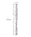
- FIG. 1 is a cross-sectional configuration diagram illustrating the configuration of a radio wave absorber according to an embodiment
- FIG. FIG. 4 is an image diagram explaining an evaluation test method for evaluating self-sustainability of the radio wave absorber according to the embodiment; It is a figure which shows the use condition of the radio wave absorber concerning embodiment.
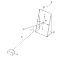
- FIG. 5 is an image diagram showing a measurement state of the relationship between the inclination angle of the radio wave incident surface of the radio wave absorber and the radio wave absorption characteristics.
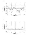
- FIG. 4 is a diagram showing changes in radio wave absorption characteristics depending on the inclination angle of the radio wave incident surface of the radio wave absorber;
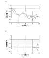
- FIG. 4 is a diagram showing changes in radio wave absorption characteristics depending on the inclination angle of the radio wave incident surface of the radio wave absorber;
- FIG. 4 is a diagram showing changes in radio wave absorption characteristics depending on the inclination angle of the radio wave incident surface of the radio wave absorber;
- FIG. 4 is a diagram showing changes in radio wave absorption characteristics depending
- a radio wave absorber disclosed in the present application is a radio wave absorber comprising a radio wave absorbing layer and a reinforcing layer disposed on the surface of the radio wave absorbing layer on the side of the radio wave incident surface, wherein the radio wave absorbing layer has a frequency of 20 GHz to At least one of magnetic iron oxide powder and carbon-based fine particles that magnetically resonate in a frequency band of 300 GHz, and a binder made of resin, the reinforcement layer is made of a dielectric material, and the radio wave absorber is mainly composed of It has a plate-like shape with a small thickness relative to the surface and can stand on its own.
- the radio wave absorber disclosed in the present application can be easily arranged so as to block the path along which the radio wave to be absorbed travels. Adverse effects can be easily avoided.
- the magnetic iron oxide powder is either magneplumbite-type ferrite powder or epsilon magnetic iron oxide powder
- the carbon-based fine particles are carbon black. , carbon nanotubes, and graphene.
- the resin binder is a rubber-based member.
- a rubber binder By using a rubber binder, it is possible to easily form a radio wave absorbing layer having a large main surface area.
- the ⁇ value which indicates the degree of deformation of the electromagnetic wave absorber sample, is 0.5 mm or less. In this case, it can be evaluated that the radio wave absorber can stand on its own.
- the radio wave attenuation amount with respect to the radio wave that passes through the radio wave absorber is -10 dB or more.
- Radio wave absorption that can sufficiently reduce the influence of unwanted radio waves by having a radio wave absorption characteristic in which the radio wave attenuation for transmitted radio waves is -10 dB or more, that is, the absolute value of the transmission attenuation (dB) is 10 or more. It can be used as a body.
- the reinforcing layer may include one selected from a reinforcing plate material having a honeycomb structure, foamed plate material, plastic cardboard, and plastic plate material.
- the radio wave absorber disclosed in the present application is a radio wave absorber using the radio wave absorber disclosed in the present application, wherein the radio wave absorber and the surface of the radio wave absorber on the side of the radio wave incident surface are maintained at a predetermined angle. a normal direction of the portion of the surface of the radio wave incident surface side located in the traveling direction of the radio wave to be absorbed by the radio wave absorber and the traveling direction of the radio wave intersect at a predetermined angle. are arranged as
- the expression that the normal direction of the surface portion of the radio wave incidence surface and the traveling direction of the radio waves “intersect at a predetermined angle” means that the normal direction of the surface portion of the radio wave incidence surface and the traveling direction of the radio waves It means that the directions do not overlap, that is, the two intersect at an angle greater than 0°.
- the radio wave absorber disclosed in the present application can maintain a state in which the radio wave incident surface of the radio wave absorber is inclined at a desired angle. It is possible to realize a radio wave absorber with high return loss while suppressing .
- the surface portion is a curved surface curved in at least one direction. If the surface is a curved surface, it is possible to reduce the amount of radio waves reflected in the incident direction of the radio waves and improve the return loss.
- the angle at which the radiation direction of the surface portion and the traveling direction of the radio waves intersect is preferably 2° or more and 20° or less, and more preferably, the intersection angle is 3° or more and 7° or less. .
- the radio wave absorbing layer contains strontium ferrite as a magnetic iron oxide powder and carbon black as a carbon-based fine particle as a radio wave absorbing member, and silicone rubber as a resin binder.
- An electromagnetic wave absorber including a radio wave absorber and a plastic sheet having a honeycomb structure made of polypropylene as a reinforcing layer will be described as an example.
- FIG. 1 is a cross-sectional view showing the configuration of the radio wave absorber described in this embodiment.
- the radio wave absorber As shown in FIG. 1, the radio wave absorber according to the present embodiment has a radio wave absorbing layer in which strontium ferrite powder 1a and carbon black fine particles 1b as radio wave absorbing members are dispersed in a silicone rubber binder 1c. 1, and a reinforcing layer 2, which is a plastic sheet having a honeycomb structure, disposed on the surface of the electromagnetic wave absorption layer on which the electromagnetic wave 20 is incident.
- the radio wave absorber according to the present embodiment is a radio wave absorber that is the sum of the thicknesses of the radio wave absorption layer 1 and the reinforcement layer 2 compared to the area (principal area) of the radio wave absorption layer 1 and the reinforcement layer 2.
- the thickness is sufficiently small, and the radio wave absorber as a whole has a plate-like shape that can be called a radio wave absorption board. More specifically, the thickness of the radio wave absorbing layer 1 is, for example, about 1 mm to 5 mm, while the thickness of the reinforcing layer 2 is about 5 mm to 30 mm.
- the main surfaces of the radio wave absorbing layer 1 and the reinforcing layer 2 are, for example, configured as rectangles (rectangles or squares) with sides of several centimeters to several tens of centimeters or several meters.
- the radio wave absorber according to this embodiment has the reinforcing layer 2 arranged on the radio wave incident side of the radio wave absorbing layer 1 and can stand on its own.
- self-supporting means that when the electromagnetic wave absorber is erected with the main surface thereof as a side surface (facing sideways), that is, the thickness of the portion corresponding to one side of the main surface of the electromagnetic wave absorber becomes the bottom surface.
- shape of the electromagnetic wave absorber does not change when the electromagnetic wave absorber is placed on a horizontal flat surface so that the main surface of the electromagnetic wave absorber is in the vertical direction. It should be noted that there is no problem in using supporting members or legs for maintaining the radio wave absorber in a self-supporting state.
- the main surface of the radio wave absorber may be maintained substantially vertically. Even if the support member is in contact with a part of the side different from the side on which it is arranged, and the main surface of the radio wave absorber is maintained in a state slightly inclined with respect to the vertical direction, the radio wave absorber can stand on its own. included in the state of
- the radio wave absorption layer 1 and the reinforcing layer 2 should be integrated so that the integration is not lost even when the radio wave absorber stands on its own. Just do it.
- the radio wave absorber can be constructed by separately producing the radio wave absorbing layer 1 and the reinforcing layer 2 and bonding them together using an adhesive means such as a silicone adhesive or double-sided tape. can.
- an adhesive means such as a silicone adhesive or double-sided tape. can.
- mechanical integration can be achieved by pinning, riveting, or screwing at a plurality of locations, or sandwiching the periphery in a frame shape.
- a radio wave absorber can be constructed by integrating the radio wave absorbing layer 1 and the reinforcing layer 2 by using means.
- the radio wave absorbing layer of the radio wave absorber according to this embodiment is formed by dispersing and mixing strontium ferrite powder 1a and carbon black powder 1b, which are radio wave absorbing members, in resin binder 1c.
- both the strontium ferrite powder, which is the magnetic iron oxide powder, and the carbon black powder, which is the carbon-based fine particles, are included. It is possible to adopt a configuration in which only one of the system fine particles is included.
- the main surface of the radio wave absorption layer is the path of the radio wave to be blocked by the radio wave absorber, the radiation angle of the unwanted radio wave from the device that is the noise source, and the direction of the radio wave from the outside to the device to be protected from the unwanted radio wave. Considering the angle of incidence, etc., one or more of them are arranged so as to have an area capable of blocking unwanted radio waves.
- the thickness of the radio wave absorbing layer is set based on the type of radio wave absorbing material contained, the density contained in the radio wave absorbing layer, and the like, and is set to a thickness that can sufficiently absorb unnecessary radio waves.
- the electromagnetic wave absorber as a whole can attenuate unwanted electromagnetic waves to 1/10, it can be considered that the minimum electromagnetic wave absorption effect is exhibited.
- the transmission attenuation amount which is the amount of attenuation of radio waves passing through the radio wave absorber, to 10 dB.
- the thickness is 1 mm to 4.5 mm. It can be about 5 mm.
- the radio wave absorber since a reinforcement layer, which will be described later, is arranged on the radio wave incident side of the radio wave absorption layer so that the radio wave absorber can stand on its own, there are no restrictions on the rigidity and strength of the radio wave absorption layer alone. For this reason, it is permissible to use a soft rubber-based member such as silicone rubber or natural rubber as a binder, even if the electromagnetic wave absorbing layer alone is easily deformed.
- magnetic iron oxide powder As the magnetic iron oxide powder used in the radio wave absorber according to the present embodiment, powders of magneplumbite ferrite and epsilon magnetic iron oxide that cause magnetic resonance with respect to radio waves in the frequency band of 20 GHz to 300 GHz are used. Good use.
- Magnetic powder of strontium ferrite (Sr--Fe) or barium ferrite (Ba--Fe) can be used as the magneplumbite-type (M-type) ferrite.
- the imaginary part ( ⁇ r′′) of the complex magnetic permeability related to radio wave absorption becomes high at a frequency at which resonance occurs when the magnetic material is magnetized at a high frequency. Since the natural resonance frequency f is proportional to the anisotropic magnetic field H A of the material, the higher the anisotropic magnetic field H A of the material, the higher the natural resonance frequency f.
- the natural resonance frequency f of barium ferrite (BaFe 12 O 19 ) is calculated to have a H A value of 1.35 MA/m to 48 GHz, and can absorb electromagnetic waves in the high GHz band.
- the value of the anisotropic magnetic field H A is controlled to control the natural resonance frequency f in the range of 5 to 150 GHz. can do.
- Epsilon magnetic iron oxide ( ⁇ -Fe 2 O 3 ) can be used as the magnetic iron oxide powder used in the radio wave absorber according to this embodiment.
- Epsilon magnetic iron oxide is a phase that appears between the alpha phase ( ⁇ -Fe 2 O 3 ) and the gamma phase ( ⁇ -Fe 2 O 3 ) in ferric oxide (Fe 2 O 3 ), and is a reverse micelle. It is a magnetic material that can be obtained in a single-phase state by a nanoparticle synthesis method that combines a method and a sol-gel method. Epsilon magnetic iron oxide is a fine particle of several nanometers to several tens of nanometers, but has a maximum coercive force of about 20 kOe as a metal oxide at room temperature. Since it occurs in the so-called millimeter wave frequency band above gigahertz, it is suitable as a radio wave absorbing material for absorbing radio waves in the millimeter wave band.
- epsilon magnetic iron oxide is a crystal in which part of the Fe site of the crystal is replaced with a trivalent metal element such as aluminum (Al), gallium (Ga), rhodium (Rh), indium (In).
- a trivalent metal element such as aluminum (Al), gallium (Ga), rhodium (Rh), indium (In).
- Epsilon magnetic iron oxide can be obtained, including those in which some Fe sites are metal-substituted. Epsilon magnetic iron oxide is available as approximately spherical or short rod-shaped particles with an average particle size of about 30 nm.
- the electromagnetic wave absorbing layer has carbon-based fine particles alone or together with the magnetic iron oxide powder described above.
- Carbon black (CB), carbon nanotube (CNT), or graphene is preferably used as the carbon-based fine particles. Any one of these carbon-based fine particles may be used alone, or two or more of them may be used in combination.
- the carbon black various conductive carbon blacks such as furnace method conductive carbon black, acetylene black, and ketjen black can be used.
- carbon nanotubes both single-wall nanotubes (SWNT) and multi-wall nanotubes (MWNT) can be used.
- SWNT single-wall nanotubes
- MWNT multi-wall nanotubes
- Graphene is a carbon material having a sheet-like structure with a thickness of one atom, in which a honeycomb-like hexagonal lattice formed by sp2 bonds of carbon atoms is laid out in a plane. Strictly speaking, graphene refers to a one-layer sheet as described above, but the graphene used for the radio wave absorbing layer described in this embodiment includes, for example, a carbon film having 2 to 1000 layers stacked. Furthermore, graphite in which graphene is laminated three-dimensionally is also included.
- Carbon-based fine particles having a specific surface area of 30 to 2,300 m 2 /g, preferably 300 to 2,000 m 2 /g, and more preferably 800 to 1,800 m 2 . /g is preferably used.
- Carbon black preferably has a primary particle diameter of 10 to 60 nm and a BET value of 300 to 1500 m 2 /g.
- the carbon nanotube preferably has a diameter of 3 to 50 nm, a length of 3 to 100 ⁇ m, and a BET value of 10 to 1200 m 2 /g.
- the binder used in the radio wave absorbing layer of the radio wave absorber according to this embodiment includes resin materials such as epoxy resin, polyester resin, polyurethane resin, acrylic resin, phenol resin, melamine resin, and rubber resin. can be used.
- a compound obtained by epoxidizing the hydroxyl groups at both ends of bisphenol A can be used as the epoxy resin.
- polyester-type urethane resin, polyether-type urethane resin, polycarbonate-type urethane resin, epoxy-type urethane resin, etc. can be used as a polyurethane-type resin.
- the acrylic resin is a methacrylic resin that includes an alkyl acrylate and/or an alkyl methacrylate having an alkyl group with a carbon number of 2 to 18, a functional group-containing monomer, and, if necessary, these A functional group-containing methacrylic polymer obtained by copolymerizing other modifying monomers that can be copolymerized with can be used.
- NR natural rubber
- IR isoprene rubber
- BR butadiene rubber
- SBR styrene-butadiene rubber
- IIR butyl rubber
- NBR ethylene-propylene rubber
- EPDM ethylene-propylene rubber
- CR chloroprene rubber
- ACM acrylic rubber
- CSR chlorosulfonated polyethylene rubber
- PUR urethane rubber
- Q fluororubber
- EVA ethylene/vinyl acetate rubber
- CO epichlorohydrin rubber
- T polysulfide rubber
- U urethane rubber
- thermoplastic elastomers such as styrene thermoplastic elastomers (SIS) have fluidity at high temperatures but have rubber elasticity at room temperature. It can be used as a binder for the electromagnetic wave absorbing layer of the electromagnetic wave absorber described in .
- SIS styrene thermoplastic elastomers
- acrylic rubber and silicone rubber can be preferably used because of their high heat resistance.
- acrylic rubber it has excellent oil resistance even in a high-temperature environment, and is relatively inexpensive and excellent in cost performance.
- silicone rubber in the case of silicone rubber, it has high cold resistance as well as heat resistance.
- it has the lowest temperature dependence of physical properties among synthetic rubbers, and is excellent in solvent resistance, ozone resistance, and weather resistance.
- thermoplastic resin having a heat resistance and a high melting point is used as the thermoplastic resin to form the electromagnetic wave absorber as a molded body
- 6T nylon 6TPA
- 10T nylon (10TPA) 12T
- Aromatic polyamides such as nylon (12TPA), MXD6 nylon (MXDPA) and their alloy materials
- PPS polyphenylene sulfide
- LCP liquid crystal polymer
- PEEK polyetheretherketone
- PEI polyetherimide
- PPSU polyphenyl Sulfone
- PS polystyrene
- PS styrene/butadiene/acrylonitrile copolymer
- ABS polypropylene
- P polyacetal
- PBT polybutylene terephthalate
- PC polycarbonate
- halogen-free resin that does not contain halogen as the resin used as the binder.
- resin materials are commonly used as binder materials for resin sheets and are readily available.
- arylsulfonic acids such as phenylphosphonic acid and phenylphosphonic acid dichloride, methylphosphonic acid, ethylphosphonic acid, and octyl Phosphoric acid compounds such as phosphonic acids, alkyl phosphonic acids such as propyl phosphonic acid, or polyfunctional phosphonic acids such as hydroxyethane diphosphonic acid, nitrotrismethylene phosphonic acid can be included as dispersants.
- phenylphosphonic acid manufactured by Wako Pure Chemical Industries, Ltd., or manufactured by Nissan Chemical Industries, Ltd.
- phosphoric acid ester "JP-502" manufactured by Johoku Chemical Industry Co., Ltd. (product name), etc.
- magneplumbite-type ferrite is used as the composition of the radio wave absorbing layer
- 2 to 120 parts of a resin binder is added to 100 parts of magneplumbite-type ferrite, and the content of the phosphoric acid compound is It can be from 0.1 to 15 parts.
- epsilon iron oxide for example, 2 to 50 parts of the resin binder and 0.1 to 15 parts of the phosphoric acid compound are used per 100 parts of the epsilon magnetic iron oxide powder. can be done. If the amount of the resinous binder is insufficient, the magnetic iron oxide cannot be well dispersed. In addition, the sheet-like shape of the magnetic layer cannot be maintained. If the amount of the resinous binder is large, the volume content of the magnetic iron oxide in the radio wave absorbing layer will be small, and the magnetic permeability will be low, so that the effect of radio wave absorption will be reduced.
- carbon black is used as the carbon-based fine particles
- 300 to 700 parts of the resin binder can be used with respect to 100 parts of carbon black.
- 300 to 2500 parts of a resin binder can be used with respect to 100 parts of carbon black or carbon nanotubes.
- the electromagnetic wave absorbing layer of the electromagnetic wave absorber of the present embodiment is formed by, for example, preparing a magnetic paint containing magnetic iron oxide powder and a resin binder, applying the magnetic paint to a predetermined thickness, drying it, and then calendering it. can be formed by
- a magnetic iron oxide powder, a phosphoric acid compound as a dispersant, and a binder resin are mixed at high speed with a high-speed stirrer to prepare a mixture, and then the resulting mixture is subjected to dispersion treatment with a sand mill.
- a magnetic paint can also be obtained by
- a radio wave absorbing layer is produced using the magnetic paint produced in this way.
- the magnetic paint prepared above is applied onto a base sheet made of resin.
- a polyethylene terephthalate (PET) sheet having a thickness of 38 ⁇ m and having a release treatment applied to the surface thereof by silicon coating can be used.
- PET polyethylene terephthalate
- a magnetic paint is applied onto this resin sheet using a coating method such as a table coater method or a bar coater method.
- the magnetic paint in a wet state is dried and further calendered to form a sheet-like radio wave absorbing layer on the support.
- the thickness of the radio wave absorbing layer can be controlled by the coating thickness, calendering conditions, and the like. After the calendering, the radio wave absorbing layer is peeled off from the resin sheet to obtain a radio wave absorbing layer having a desired thickness.
- calendering may be performed as necessary, and calendering may not be performed when the volume content of the radio wave absorbing material is within a predetermined range when the magnetic paint is dried. .
- the radio wave absorbing layer As another manufacturing method of the radio wave absorbing layer, magnetic iron oxide powder and/or carbon-based fine particles are kneaded with a resin binder, and the resulting kneaded product is mixed with a cross-linking agent to adjust the viscosity.
- the obtained magnetic compound is crosslinked and molded into a sheet at a temperature of 165° C. using a hydraulic press or the like, and then subjected to secondary crosslinking treatment in a constant temperature bath or the like to form a radio wave absorbing layer. can.
- extrusion molding and injection molding can be used for molding.
- a radio wave absorbing material, a resin binder, and, if necessary, a dispersant, etc. are blended in advance using a pressurized kneader, extruder, roll mill, etc., and these blended materials are fed to the resin supply port of an extruder. from into the plastic cylinder.
- a normal extruder equipped with a plastic cylinder, a die provided at the tip of the plastic cylinder, a screw rotatably disposed in the plastic cylinder, and a drive mechanism for driving the screw A molding machine can be used.
- the molten material plasticized by the band heater of the extruder is fed forward by the rotation of the screw and extruded from the tip in the form of a sheet to obtain a radio wave absorbing layer with a predetermined thickness.
- a radio wave absorbing substance, a dispersant, and a binder are pre-blended as needed, and the blended materials are fed into the plastic cylinder from the resin supply port of the injection molding machine, and melted and kneaded with a screw in the plasticization cylinder. After that, a molded body can be formed by injecting molten resin into a mold connected to the tip of an injection molding machine.
- a roll-to-roll method can be used in which molding is performed while moving between two rolls.
- the roll-to-roll method it is possible to produce a sheet-like electromagnetic wave absorbing layer with a width of about 1 m to 3 m. can be realized.
- the reinforcing layer is a molded body of a dielectric material, and is a plate-like member having a small thickness with respect to the area of the main surface.
- the reinforcing layer is heavy, the weight of the radio wave absorber as a whole increases.
- Texel (trade name, manufactured by Gifu Plastic Industry Co., Ltd.), which is a honeycomb core material formed of polypropylene (PP), is suitable for the reinforcing layer.
- PP polypropylene
- Texel has a honeycomb structure sandwiched between two thin flat layers, so it is lightweight but has high strength (rigidity).
- Texel is commercially available with a thickness of 5 mm to 30 mm, a maximum width of 1,250 mm, and a maximum length of 2,500 mm. can be obtained.
- various resin boards can be used as the reinforcing layer of the radio wave absorber according to this embodiment.
- PALLONIA registered trademark, manufactured by Mitsui Chemicals Tohcello, Inc.
- PALLONIA foam-molded polypropylene
- it can be effectively used as a reinforcing layer as a plate material made of a dielectric material having a light specific gravity and a certain level of strength.
- plastic corrugated cardboard made of polypropylene can also be used as a reinforcing layer as a member that is lightweight yet has a certain amount of rigidity.
- the above-mentioned reinforcing plate material, foam plate material, and plastic corrugated cardboard which have a honeycomb structure, are lightweight due to the presence of cavities inside the plate material. It is characterized by a low dielectric constant.
- a reinforcing layer is arranged on the surface of the radio wave absorbing layer on the side on which radio waves are incident. At this time, since the dielectric constant of the reinforcement layer is sufficiently low, reflection of incident radio waves on the surface of the reinforcement layer is reduced, and more radio waves enter the radio wave absorption layer and are absorbed by the radio wave absorption layer. Become.
- the radio waves emitted from the transmitter are reflected on the surface of the radio wave absorber and Therefore, it is possible to effectively suppress the reception of the radio wave at a high S/N ratio, and to measure the radio wave characteristics.
- a plastic plate such as an acrylic plate or a polycarbonate plate can also be used for the reinforcing layer.
- the specific gravity is large, and the weight increases as a reinforcing layer to which a large-area radio wave absorbing layer is fixed.
- the radio wave absorber is allowed to stand on its own, it may bend due to its own weight. Therefore, it is an effective material as a reinforcing layer used together with a radio wave absorption layer having a relatively small main surface.
- the reinforcing layer has a bending strength of 3 MPa or more according to the bending fracture test method, a flexible radio wave absorbing layer that can be easily bent like a radio wave absorbing layer using a rubber material as a binder. It has been confirmed that, even if the material is used in combination with the reinforcing layer, it is possible to obtain practically sufficient rigidity that allows the radio wave absorber to stand on its own.
- the dielectric material used as the reinforcing layer has a water absorption rate of 1.5% or less.
- the radio wave absorber according to the present embodiment is self-supporting because its main surface can be maintained substantially vertically. Accordingly, the inventors devised an evaluation method for quantifying and evaluating the degree of self-sustainability of the radio wave absorber according to this embodiment.
- FIG. 2 is a model diagram explaining a measurement method for evaluating the self-sustainability of the radio wave absorber according to this embodiment.
- a radio wave absorber 21 with a width of 25 mm and a length of 100 mm is used as a sample.
- the ⁇ value obtained in this way which indicates the degree of deformation of the radio wave absorber sample, is 0.5 mm or less, it is evaluated as being in a self-supporting state.
- Radio wave absorption layer As the radio wave absorbing layer, strontium ferrite magnetic powder was used as the magnetic iron oxide powder, and the type of the carbon-based fine particles was changed. Silicone rubber was used as the binder in each case.
- the electromagnetic wave absorbing layer was produced by press-molding a magnetic compound with a predetermined thickness.
- the magnetic compound was obtained by kneading a magnetic iron oxide powder, a rubber binder, and carbon-based fine particles, and mixing a cross-linking agent with the resulting kneaded product to adjust the viscosity.
- the magnetic compound thus produced was crosslinked and molded into a sheet at a temperature of 165°C using a hydraulic press, and then subjected to a secondary crosslinking treatment at a temperature of 170°C in a constant temperature bath. A desired radio-absorbing layer of the indicated thickness was obtained.
- the materials and amounts of the magnetic iron oxide powder, carbon-based fine particles, and rubber binder used to form the magnetic compound were as follows.
- Radio wave absorption layer 1 Magnetic iron oxide Strontium ferrite magnetic powder 65 parts by weight Carbon-based fine particles Carbon black 1.5 parts by weight Binder Silicone rubber: KE-541-U 33 parts by weight Crosslinking agent 0.5 parts by weight Radio wave absorbing layer 2 Magnetic iron oxide Strontium ferrite magnetic powder 65 parts by weight Carbon-based fine particles Carbon nanotube 1.5 parts by weight Binder Silicone rubber: KE-541-U 33 parts by weight Crosslinking agent 1 part by weight Radio wave absorbing layer 3 Magnetic iron oxide Strontium ferrite magnetic powder 65 parts by weight Binder Silicone rubber: KE-541-U 34 parts by weight Crosslinking agent 1 part by weight Radio wave absorption layer 4 Carbon-based fine particles Carbon black 6 parts by weight Binder Silicone rubber: KE-541-U 92 parts by weight Cross-linking agent 2 parts by weight.
- Strontium ferrite magnetic powder having an average particle size of 2.2 ⁇ m and a BET value of 1.5 m 2 /g was used as each material of the radio wave absorbing layer.
- carbon black Ketjenblack EC600JD (product name) manufactured by Lion Specialty Chemicals Co., Ltd. having a primary particle size of 34 nm and a BET value of 1400 m 2 /g was used.
- carbon nanotube VGCF-H (product name) manufactured by Showa Denko K.K. and having a fiber diameter of 150 nm and a BET value of 13 m 2 /g was used.
- the silicone rubber KE-541-U (product name) used as a binder is a silicone rubber manufactured by Shin-Etsu Chemical Co., Ltd.
- As a cross-linking agent 2.5 dimethyl-2.5 bis(tertiarybutylperoxy)hexane (C-8A (product name) manufactured by Shin-Etsu Chemical Co., Ltd.) was used.
- the honeycomb core material made of polypropylene (Texel (trade name, manufactured by Gifu Plastic Industry Co., Ltd.)) having a thickness of 9.7 mm (reinforcing layer 1) and having a thickness of 7.7 mm (reinforcing layer 1) are used.
- Layer 2) 6.0 mm thick polypropylene foam molded body (Palonia (registered trademark, manufactured by Mitsui Chemicals Tohcello Co., Ltd.) (reinforcing layer 3), 10.0 mm thick acrylic plate (reinforcing layer 4) , a plastic cardboard (reinforcing layer 5) having a thickness of 10.0 mm was prepared.
- ⁇ self-sustainability evaluation value
- Example 1 is radio wave absorbing layer 1 and reinforcing layer 1
- Example 2 is radio wave absorbing layer 1 and reinforcing layer 2
- Example 3 is radio absorbing layer 1 and reinforcing layer 3
- Example 4 is a radio wave absorbing layer 3 and a reinforcing layer 1
- Example 5 is a radio wave absorbing layer 1 and a reinforcing layer 4
- Example 6 is a radio wave absorbing layer 2 and a reinforcing layer 1
- Example 7 is a radio wave absorbing layer 1 and a reinforcing layer. 5.
- the electromagnetic wave absorbing layer 4 and the reinforcing layer 1 were combined, each having a width of 25 mm and a length of 100 mm. Further, in Comparative Example 1, the radio wave absorbing layer 1 was used as the radio wave absorbing layer.
- Both the return loss and transmission loss of radio waves were measured using the free space method. Specifically, using a millimeter wave network analyzer ME7838A (product name) manufactured by Anritsu Co., Ltd., the radio wave incident surface side, which is the front side of the radio wave absorber, from the transmitting antenna through the dielectric lens, that is, the reinforcing layer An input wave of 76.5 GHz was applied to the arranged side. At this time, the surface reflected wave reflected by the front surface of the radio wave absorber and the transmitted wave penetrating the back side of the radio wave absorber, ie, the side of the radio wave absorbing layer, were respectively measured by arranging receiving antennas. The strength of the radio wave emitted from the transmitting antenna and the strength of the radio wave received by the receiving antenna are measured as voltage values, respectively. The transmission attenuation amount was obtained in dB from "wave-transmitted wave".
- Table 1 shows the above measurement results.
- the self-supportability evaluation value ⁇ is 0.5 or less, and it can be judged that the self-reliance is sufficient.
- the transmission attenuation amount when passing through a radio wave absorber exhibiting radio wave absorption characteristics was -10 dB or more in any of the examples, confirming that they have practically sufficient radio wave absorption characteristics.
- the radio wave absorber of Comparative Example 1 which does not have a reinforcing layer, has a self-sustainability evaluation value ⁇ of 12 mm, which is extremely large. Recognize.
- the radio wave absorber according to the present embodiment can stand on its own by providing the reinforcing layer on the radio wave incident side of the radio wave absorbing layer, and can be easily arranged at a desired position. It was confirmed that a radio wave absorber was obtained.
- A is the return loss (dB) on the surface of the reinforcing layer that is the front surface of the radio wave absorber, and the return loss on the surface of the radio wave absorption layer that is the back surface of the radio wave absorber (from the back side)
- the value of the ratio A/B is 1.5 or more and 6.5 or less, where B is the attenuation amount (dB) of the radio wave reflected on the surface of the radio wave absorbing layer when the radio wave is irradiated. was confirmed.
- Radio wave absorber A radio wave absorber that absorbs unwanted radio waves using the radio wave absorber according to the present embodiment will be described below with specific examples.
- the radio wave absorber disclosed in the present application can stand on its own because it has a reinforcing layer having a predetermined thickness and rigidity together with the radio wave absorbing layer. Taking advantage of this fact, for example, when measuring the radio wave characteristics of a device to be measured, by placing a radio wave absorber on the path between unwanted radio waves reflected by a wall and the measuring device, the measurement It is possible to effectively prevent the measuring instrument from catching radio waves other than the radio waves from the device to be measured, and to measure radio wave characteristics with a high S/N ratio.
- the radio wave absorber When a radio wave absorber is placed on the path between an unwanted radio wave and a measuring instrument, the radio wave absorber can stand alone, but the radio wave absorber can be easily moved to a desired position. Considering that the arrangement position and arrangement direction are maintained, the practicality is greatly improved by using a radio wave absorber with support members such as legs and struts fixed to the radio wave absorber rather than the radio wave absorber alone. It is preferable because it improves.
- the support member may be any member that can maintain the position of the radio wave absorber, the orientation and inclination of the radio wave incident surface, and the like, in a state in which the radio wave absorber can effectively absorb unwanted radio waves.
- the support member may be of any suitable form, such as a member that suspends the radio wave absorber from the ceiling surface or a wall surface, a member that holds the end of the radio wave absorber, or the like. can be selected.
- the radio wave absorber since the reinforcement layer formed of a dielectric material is arranged on the radio wave incident surface side of the radio wave absorption layer, as described in the above embodiment, the radio wave absorber is incident on Part of the radio wave is reflected on the surface of the reinforcing layer.
- the inventors have found that the reflection characteristics of radio waves on the surface of this reinforcing layer change depending on the angle of inclination of the radio wave incident surface with respect to radio waves incident on the radio wave absorber.
- FIG. 3 is a diagram showing a state in which a radio wave absorber is tilted as an example of the radio wave absorber according to this embodiment.
- the radio wave absorber 30 illustrated in FIG. 3 includes a plate-like radio wave absorber 31 and two side portions of the radio wave absorber 31 which are perpendicular to the radio wave incident surface, which is the main surface of the radio wave absorber 31 . It consists of two triangular support members 32 mounted so as to extend sideways. By providing the supporting member 32 in this way, the electromagnetic wave absorber 30 can be easily moved to a predetermined position in a predetermined direction while maintaining the state in which the radio wave incident surface of the electromagnetic wave absorber 31 is inclined at a predetermined angle. can be placed in
- the angle of inclination of the radio wave absorber 31 in the radio wave absorber 30 refers to the traveling direction of the radio wave 34 to be absorbed (incident direction to the radio wave absorber 31) and the traveling direction of this radio wave.
- the direction of radiation on the surface of the radio wave absorber on the side of the radio wave incident surface and the traveling direction of radio waves intersect at a predetermined angle, that is, ⁇ is not 0°. It is characterized.
- the traveling direction 34 of the absorbed radio wave is understood to be the direction of a straight line connecting the radio wave emitting source (device 33 in the case of FIG. 3) and the radio wave absorber 31 so as to minimize the distance. can do.
- the portion 31a on the radio wave incident surface side of the radio wave absorber 31 is a portion with a small area located in the traveling direction of the radio waves obtained as described above, and its size is, for example, the same as that of the radio wave emission source 33. It can be considered as a circular portion having a diameter about 1/100 of the distance from the electromagnetic wave absorber 30 (a circular portion with a diameter of 3 cm when the distance is 3 m).
- the electromagnetic wave absorber is not flat, that is, when the surface of the electromagnetic wave absorber is curved rather than flat, similarly, the portion of the electromagnetic wave absorber on the side of the electromagnetic wave incident surface in the traveling direction of the absorbed electromagnetic wave
- the angle formed by the normal direction and the traveling direction of radio waves is defined as the inclination angle ⁇ of the radio wave absorber.
- the curved direction is horizontal (X direction in FIG. 3), vertical (Y direction in FIG. 3), or X A direction other than the direction and the Y direction is also possible. Furthermore, a substantially spherical surface, that is, curved in both the X direction and the Y direction, is also conceivable. However, in any of these cases, since it is possible to determine the normal direction of the portion of the wave absorber on the side of the wave incident surface that is positioned in the propagation direction of the wave, the tilt angle of the wave absorber is determined according to the above definition. be able to.
- the surface of the radio wave absorber is a curved surface
- the surface is convex on the side on which radio waves are incident, and the case is concave on the side on which radio waves are incident.
- the inclination angle of the wave absorber can be determined by the above definition.
- the surface of the electromagnetic wave absorber when the surface of the electromagnetic wave absorber has different heights, such as uneven or corrugated shape, the surface of the electromagnetic wave absorber is defined as a plane using the average value of the heights, and the propagation of the electromagnetic wave is calculated.
- the inclination angle of the radio wave absorber can be determined by determining the normal direction of the portion on the side of the radio wave incident surface in the direction.
- the return loss which is the radio wave characteristic of the radio wave absorber to be examined here, is the strength of the radio wave transmitted from the device that transmits the radio wave. It is a numerical value (dB) that indicates how much the strength of the radio wave that has been transmitted has decreased, and the measurement method is as described above. be measured. Considering that radio waves propagate in a straight line but spread radially, a wave absorber with a curved or uneven surface absorbs radio waves better than a flat surface. The radio waves reflected by the surface of the body are less likely to scatter and return to the source.
- the surface portion of the radio wave absorber in the traveling direction of the radio wave should be flat.
- a curved surface curved in at least one direction is preferable. That is, the return loss can be further reduced by forming a curved surface in which the normal direction of the surface portion of the electromagnetic wave absorber is inclined with respect to the traveling direction of the radio waves, rather than by making the surface portion of the electromagnetic wave absorber an inclined plane. Conceivable.
- FIG. 4 is a schematic diagram showing a measurement system for measuring the relationship between the inclination angle of the radio wave absorber and the radio wave absorption characteristics.
- the change in the radio wave characteristics at the inclination angle of the radio wave absorber was measured by the free space method using a millimeter wave network analyzer ME7838A (product name: code 41) manufactured by Anritsu Co., Ltd., the same as that described in the embodiment of the radio wave absorber. measured in
- the radio wave incident surface side which is the front side of the radio wave absorber 40, that is, the side where the reinforcing layer is arranged, is provided with 76.76.
- An input wave of 5 GHz (reference numeral 46) was applied.
- the surface reflected wave S 11 (reference numeral 47) reflected by the front surface of the radio wave absorber 40 was received by the receiving antenna (reference numeral 42) through the dielectric lens 43.
- the angle ⁇ of the radio wave absorber 40 is gradually inclined from 0°, ie, the state of being vertically arranged, to 20°, the intensity of the radio wave emitted from the transmitting antenna 42 and the intensity of the radio wave received by the receiving antennas 42 and 45 are measured.
- the intensity of the radio wave was measured as a voltage value, and the reflection attenuation on the surface of the radio wave absorber and the transmission attenuation through the radio wave absorber were each determined in dB.
- Figures 5 to 7 show the measurement results of the tilt angle and return loss, and the tilt angle and transmission loss of each radio wave absorber.
- the change in return loss with respect to the change in the tilt angle of the wave absorber is represented as (a) in each figure, and the change in transmission attenuation with respect to the change in the tilt angle of the wave absorber. is represented as (b) in each figure.
- the horizontal axis indicates the inclination angle ⁇ (°) of the radio wave absorber
- the vertical axis indicates the radio wave attenuation (dB).
- the above-described polypropylene honeycomb core material (Texel T10-2000 (trade name, manufactured by Gifu Plastic Industry Co., Ltd., 9.7 mm thick: reinforcing layer 1)) is used as the reinforcing layer, and the radio wave absorbing layer
- the measurement results are shown when the above-described "radio wave absorbing layer 1" is used as the (same as the radio wave absorber of Example 1).
- the return loss is Compared to the case where the inclination angle is 0°, that is, when the light is incident on the surface of the electromagnetic wave absorber perpendicularly, the return loss becomes larger when the inclination angle is up to 20°.
- the value of return loss does not increase uniformly, but the value of return loss rises and falls in a wave-like manner, and there is a range in which a larger return loss can be obtained. It can be seen that In particular, it can be confirmed that the reflection attenuation of the TE wave is 50 dB or more in the vicinity of the inclination angles of 5° and 13°, showing extremely large radio wave absorption characteristics.
- FIG. 5(b) which shows changes in the amount of transmission attenuation
- the polarization direction of the irradiated wave is the TE (electric field) wave.
- a constant value of about -15 dB is shown for any of the dashed lines 54 whose direction indicates the TM (magnetic field) wave.
- Fig. 6 shows a resin board (Plastar ( PGPPZ-200 (trade name, manufactured by Kawakami Sangyo Co., Ltd., thickness 9 mm) is used, and the above-mentioned "radio wave absorption layer 1" is used as the radio wave absorption layer.
- Plastar PGPPZ-200 (trade name, manufactured by Kawakami Sangyo Co., Ltd., thickness 9 mm) is used, and the above-mentioned "radio wave absorption layer 1" is used as the radio wave absorption layer.
- the return loss is Compared to the case where the inclination angle is 0°, that is, when the light is incident on the surface of the electromagnetic wave absorber perpendicularly, the return loss becomes larger when the inclination angle is up to 20°. Further, as the tilt angle increases, the value of the return loss fluctuates slightly and changes to a large value as a whole. It can be seen that there is a region where both the solid line 61 indicating the electric field and the dotted line 62 indicating the electric field have large values around the tilt angle of 5° to 7°.
- FIG. 6(b) which shows changes in the amount of transmission attenuation
- FIG. 6(b) which shows changes in the amount of transmission attenuation
- a constant value of about -15 dB is shown for both the solid line 63 indicating the polarization direction of the TE (electric field) wave and the dashed line 64 indicating the polarization direction of the TM (magnetic field) wave.
- FIG. 7 shows, as a reinforcing layer, a resin-made hollow structural plate (dan plate (registered trademark)) in which polypropylene plastic corrugated cardboards are arranged side by side with vertical walls arranged in one direction and covered with upper and lower flat plates.
- dan plate registered trademark
- J-10-180 trade name, manufactured by Ube Exsimo Co., Ltd., thickness 10 mm
- the above-described “radio wave absorption layer 1” is used as the radio wave absorption layer.
- the return loss is Compared to the case where the inclination angle is 0°, that is, when the light is incident on the surface of the electromagnetic wave absorber perpendicularly, the return loss becomes larger when the inclination angle is up to 20°.
- the hollow structural plate shown in FIG. 7(a) is used as the reinforcing layer, the change in the return loss due to the change in the tilt angle is the largest, and the change is wavy, but the tilt angle is 4° to 7°. It can be seen that there is a region around ° where both the solid line 71 indicating the electric field and the dotted line 72 indicating the electric field have large values.
- FIG. 7B which shows changes in transmission attenuation
- the polarization direction of the irradiation wave is about 12 dB in the solid line 73 indicating the TE (electric field) wave
- the polarization direction is the TM (magnetic field) wave. indicates a constant value of about -14 dB.
- the return loss of radio waves reflected by the surface of the reinforcing layer disposed on the radio wave incident surface side of the radio wave absorber is It can be seen that the tilted state is greater than the non-tilted state (tilt angle is 0°).
- the magnitude of change in the return loss varies depending on the shape of the space inside the reinforcing layer, the return loss does not gradually increase according to the tilt angle, but the tilt angle region where the return loss increases, It has been confirmed that there is a region with a tilt angle in which the return loss is relatively small. As shown in FIGS. 5 to 7, it was confirmed that the return loss increased in the range of the inclination angle of 3° or more and 7° or less.
- the tendency of change in return loss with respect to the angle of the incident radio wave differs depending on the configuration of the reinforcing layer, particularly depending on the arrangement of the air contained in the reinforcing layer. It should be noted that, as in the honeycomb core material shown in FIG. 5 and the plastic corrugated cardboard shown in FIG. Compared to the resin board of the air cap shown, where air is confined in a space limited in the thickness direction, it is thought that the degree of increase and decrease in return loss with respect to the tilt angle is greater.
- a partition member that is not divided in the thickness direction is arranged between the upper and lower flat plates, in addition to a honeycomb shape and a linear shape in one direction, a grid shape and rhombus that intersect at right angles vertically and horizontally are formed. It is assumed that the change tendency of the return loss due to the inclination angle is similar regardless of the shape of the partition member, such as a lattice shape that intersects obliquely, or a shape in which a plurality of cylinders are lined up. Further, for example, in the case where the tips of conical members arranged on both the upper plate member and the lower plate member are joined together to form a separating member, or the separating member is arranged in a wavy shape in the thickness direction. , it is presumed that, like the resin board shown in FIG.
- the reinforcing layer is made of foam, it is considered that the degree of change in the return loss with respect to the change in the tilt angle is the smallest. It is thought that the amount of attenuation can be increased.
- the radio wave absorber shown in this embodiment is a radio wave absorber in which at least one of magnetic iron oxide and carbon-based fine particles that perform magnetic resonance in a frequency band of 20 GHz to 300 GHz is dispersed and mixed in a resin binder. and a reinforcing layer made of a dielectric material and arranged on the side of the radio wave absorption layer on which radio waves are incident. Self-supporting. For this reason, for example, when measuring radio wave characteristics, it is possible to protect the measuring device and the device to be measured from unwanted radio waves by arranging it in a position that blocks unnecessary radio waves, such as in a good environment with little noise. It is possible to measure the radio wave characteristics at
- the radio wave absorber shown in this embodiment is a radio wave absorber using the radio wave absorber disclosed in the present application. It is provided with a support member that can be maintained, and is arranged so that the normal direction of the portion of the surface on the side of the radio wave incidence surface located in the traveling direction of the absorbed radio waves and the traveling direction of the radio waves intersect at a predetermined angle. For this reason, the radio wave absorber can be easily maintained in a state of being tilted at a predetermined tilt angle, the reflection of radio waves on the surface of the reinforcing layer is suppressed, the return attenuation characteristics are excellent, and the radio wave absorber can be positioned at a desired position. A radio wave absorber that can be easily arranged can be realized.
- the main surfaces of the radio wave absorbing layer and the reinforcing layer of the radio wave absorber have been described as being rectangular with the same size. It does not have to be the same, and as long as the shape can sufficiently block the path of unwanted radio waves that you want to block with the radio wave absorber, there is no problem even if one of them is larger than the other and a part of it protrudes. There is no In addition, even if the planar shape of the radio wave absorbing layer is complicated with protrusions, recesses, and voids, as long as the reinforcing layer can maintain its entirety in a substantially vertical direction, it will absorb radio waves. A reinforcing layer having a planar shape such as a rectangle, circle, or polygon larger than the absorption may be used.
- the radio wave absorber disclosed in the present application can absorb radio waves of 20 GHz to 300 GHz well and can stand on its own, so it can be easily placed in the path of radio waves to be absorbed. Further, a radio wave absorber capable of maintaining a state in which the radio wave absorber is tilted at a predetermined tilt angle can be easily used in a state in which the reflection of radio waves on the surface of the reflective layer is reduced. Therefore, it is useful as a radio wave absorbing member capable of forming a good space in which the influence of unwanted radio waves is suppressed.
Landscapes
- Engineering & Computer Science (AREA)
- Chemical & Material Sciences (AREA)
- Physics & Mathematics (AREA)
- Electromagnetism (AREA)
- Microelectronics & Electronic Packaging (AREA)
- Dispersion Chemistry (AREA)
- Power Engineering (AREA)
- Crystallography & Structural Chemistry (AREA)
- Computer Networks & Wireless Communication (AREA)
- Signal Processing (AREA)
- Shielding Devices Or Components To Electric Or Magnetic Fields (AREA)
Priority Applications (3)
| Application Number | Priority Date | Filing Date | Title |
|---|---|---|---|
| US18/275,714 US20250331141A1 (en) | 2021-02-04 | 2022-02-02 | Electric-wave absorber and electric-wave absorbing device |
| JP2022579588A JP7847546B2 (ja) | 2021-02-04 | 2022-02-02 | 電波吸収体、および電波吸収装置 |
| EP22749756.7A EP4290995A4 (en) | 2021-02-04 | 2022-02-02 | RADIO WAVE ABSORBER AND RADIO WAVE ABSORBER DEVICE |
Applications Claiming Priority (4)
| Application Number | Priority Date | Filing Date | Title |
|---|---|---|---|
| JP2021-016906 | 2021-02-04 | ||
| JP2021016906 | 2021-02-04 | ||
| JP2021149155 | 2021-09-14 | ||
| JP2021-149155 | 2021-09-14 |
Publications (1)
| Publication Number | Publication Date |
|---|---|
| WO2022168885A1 true WO2022168885A1 (ja) | 2022-08-11 |
Family
ID=82741535
Family Applications (1)
| Application Number | Title | Priority Date | Filing Date |
|---|---|---|---|
| PCT/JP2022/004120 Ceased WO2022168885A1 (ja) | 2021-02-04 | 2022-02-02 | 電波吸収体、および電波吸収装置 |
Country Status (4)
| Country | Link |
|---|---|
| US (1) | US20250331141A1 (https=) |
| EP (1) | EP4290995A4 (https=) |
| JP (1) | JP7847546B2 (https=) |
| WO (1) | WO2022168885A1 (https=) |
Cited By (2)
| Publication number | Priority date | Publication date | Assignee | Title |
|---|---|---|---|---|
| TWI860187B (zh) * | 2023-11-30 | 2024-10-21 | 大陸商宏啟勝精密電子(秦皇島)有限公司 | 耐彎折電路板及其製備方法 |
| WO2025028488A1 (ja) * | 2023-08-03 | 2025-02-06 | マクセル株式会社 | 電磁波吸収体 |
Citations (8)
| Publication number | Priority date | Publication date | Assignee | Title |
|---|---|---|---|---|
| JP2004003259A (ja) * | 2001-08-31 | 2004-01-08 | Tdk Corp | 電波音波吸収体、電波音波吸収パネル、電波吸収防音壁、道路付帯設備ならびに電波および音波の反射抑制方法 |
| JP2005109095A (ja) * | 2003-09-30 | 2005-04-21 | Tdk Corp | 不要電波抑制構造及び電波吸収仕切壁 |
| JP2008060484A (ja) | 2006-09-01 | 2008-03-13 | Univ Of Tokyo | 電波吸収性磁性結晶および電波吸収体 |
| JP2009239211A (ja) * | 2008-03-28 | 2009-10-15 | Mitsubishi Cable Ind Ltd | 電波吸収シートおよびその設置方法 |
| JP2016111341A (ja) | 2014-12-03 | 2016-06-20 | 国立大学法人 東京大学 | 電磁波吸収体及び膜形成用ペースト |
| WO2017221992A1 (ja) | 2016-06-22 | 2017-12-28 | 日立マクセル株式会社 | 電波吸収シート |
| WO2018084235A1 (ja) | 2016-11-04 | 2018-05-11 | マクセルホールディングス株式会社 | 電磁波吸収シート |
| WO2019235364A1 (ja) * | 2018-06-06 | 2019-12-12 | 国立大学法人 東京大学 | 電波吸収積層フィルム、その製造方法、及びそれを含む素子 |
Family Cites Families (4)
| Publication number | Priority date | Publication date | Assignee | Title |
|---|---|---|---|---|
| JPH0312500U (https=) * | 1989-06-22 | 1991-02-07 | ||
| JPH0314294U (https=) * | 1989-06-27 | 1991-02-13 | ||
| EP3606309B1 (en) * | 2017-03-30 | 2023-09-06 | FUJIFILM Corporation | Electromagnetic wave absorber and method for producing electromagnetic wave absorber |
| US11804659B2 (en) * | 2017-07-20 | 2023-10-31 | Maxell, Ltd. | Electromagnetic wave absorbing composition, and electromagnetic wave absorption body |
-
2022
- 2022-02-02 EP EP22749756.7A patent/EP4290995A4/en active Pending
- 2022-02-02 JP JP2022579588A patent/JP7847546B2/ja active Active
- 2022-02-02 WO PCT/JP2022/004120 patent/WO2022168885A1/ja not_active Ceased
- 2022-02-02 US US18/275,714 patent/US20250331141A1/en active Pending
Patent Citations (8)
| Publication number | Priority date | Publication date | Assignee | Title |
|---|---|---|---|---|
| JP2004003259A (ja) * | 2001-08-31 | 2004-01-08 | Tdk Corp | 電波音波吸収体、電波音波吸収パネル、電波吸収防音壁、道路付帯設備ならびに電波および音波の反射抑制方法 |
| JP2005109095A (ja) * | 2003-09-30 | 2005-04-21 | Tdk Corp | 不要電波抑制構造及び電波吸収仕切壁 |
| JP2008060484A (ja) | 2006-09-01 | 2008-03-13 | Univ Of Tokyo | 電波吸収性磁性結晶および電波吸収体 |
| JP2009239211A (ja) * | 2008-03-28 | 2009-10-15 | Mitsubishi Cable Ind Ltd | 電波吸収シートおよびその設置方法 |
| JP2016111341A (ja) | 2014-12-03 | 2016-06-20 | 国立大学法人 東京大学 | 電磁波吸収体及び膜形成用ペースト |
| WO2017221992A1 (ja) | 2016-06-22 | 2017-12-28 | 日立マクセル株式会社 | 電波吸収シート |
| WO2018084235A1 (ja) | 2016-11-04 | 2018-05-11 | マクセルホールディングス株式会社 | 電磁波吸収シート |
| WO2019235364A1 (ja) * | 2018-06-06 | 2019-12-12 | 国立大学法人 東京大学 | 電波吸収積層フィルム、その製造方法、及びそれを含む素子 |
Non-Patent Citations (1)
| Title |
|---|
| See also references of EP4290995A4 |
Cited By (2)
| Publication number | Priority date | Publication date | Assignee | Title |
|---|---|---|---|---|
| WO2025028488A1 (ja) * | 2023-08-03 | 2025-02-06 | マクセル株式会社 | 電磁波吸収体 |
| TWI860187B (zh) * | 2023-11-30 | 2024-10-21 | 大陸商宏啟勝精密電子(秦皇島)有限公司 | 耐彎折電路板及其製備方法 |
Also Published As
| Publication number | Publication date |
|---|---|
| EP4290995A1 (en) | 2023-12-13 |
| EP4290995A4 (en) | 2025-01-01 |
| JPWO2022168885A1 (https=) | 2022-08-11 |
| US20250331141A1 (en) | 2025-10-23 |
| JP7847546B2 (ja) | 2026-04-17 |
Similar Documents
| Publication | Publication Date | Title |
|---|---|---|
| JP6764465B2 (ja) | 電波吸収シート | |
| US11515643B2 (en) | Electromagnetic-wave-absorbing sheet | |
| US11766854B2 (en) | Composite material for shielding electromagnetic radiation, raw material for additive manufacturing methods and a product comprising the composite material, as well as a method of manufacturing the product | |
| JP7030694B2 (ja) | 電磁波吸収体 | |
| US8133404B2 (en) | Electromagnetic wave shielding material and sheet | |
| US20200008328A1 (en) | Electromagnetic-wave absorbing sheet | |
| JPWO2019017471A1 (ja) | 電磁波吸収性組成物、電磁波吸収体 | |
| JP4108677B2 (ja) | 電磁波吸収体 | |
| WO2022168885A1 (ja) | 電波吸収体、および電波吸収装置 | |
| JP4528334B2 (ja) | 電磁波吸収体 | |
| JP2018056492A (ja) | 電波吸収シート | |
| JP2005012204A (ja) | 電磁波吸収体 | |
| JPWO2022168885A5 (https=) | ||
| WO2019235393A1 (ja) | 電磁波吸収体 | |
| JPWO2019065252A1 (ja) | 電磁波吸収体用組成物、および、電磁波吸収体 | |
| JPWO2019235539A1 (ja) | 電磁波吸収体、および、電磁波吸収体用組成物 | |
| KR102427938B1 (ko) | 레이더 흡수 복합재료 구조체 및 그 제조 방법 | |
| KR20180013625A (ko) | 전자기파 차폐시트용 조성물 및 전자기파 차폐시트 | |
| JPWO2025028488A5 (https=) | ||
| CN121420635A (zh) | 电磁波吸收体 |
Legal Events
| Date | Code | Title | Description |
|---|---|---|---|
| 121 | Ep: the epo has been informed by wipo that ep was designated in this application |
Ref document number: 22749756 Country of ref document: EP Kind code of ref document: A1 |
|
| ENP | Entry into the national phase |
Ref document number: 2022579588 Country of ref document: JP Kind code of ref document: A |
|
| NENP | Non-entry into the national phase |
Ref country code: DE |
|
| ENP | Entry into the national phase |
Ref document number: 2022749756 Country of ref document: EP Effective date: 20230904 |
|
| WWP | Wipo information: published in national office |
Ref document number: 18275714 Country of ref document: US |