WO2022163296A1 - 撮像装置 - Google Patents
撮像装置 Download PDFInfo
- Publication number
- WO2022163296A1 WO2022163296A1 PCT/JP2021/048888 JP2021048888W WO2022163296A1 WO 2022163296 A1 WO2022163296 A1 WO 2022163296A1 JP 2021048888 W JP2021048888 W JP 2021048888W WO 2022163296 A1 WO2022163296 A1 WO 2022163296A1
- Authority
- WO
- WIPO (PCT)
- Prior art keywords
- color
- pixel
- pixels
- lens
- imaging device
- Prior art date
- Legal status (The legal status is an assumption and is not a legal conclusion. Google has not performed a legal analysis and makes no representation as to the accuracy of the status listed.)
- Ceased
Links
Images
















Classifications
-
- H—ELECTRICITY
- H04—ELECTRIC COMMUNICATION TECHNIQUE
- H04N—PICTORIAL COMMUNICATION, e.g. TELEVISION
- H04N23/00—Cameras or camera modules comprising electronic image sensors; Control thereof
- H04N23/10—Cameras or camera modules comprising electronic image sensors; Control thereof for generating image signals from different wavelengths
- H04N23/12—Cameras or camera modules comprising electronic image sensors; Control thereof for generating image signals from different wavelengths with one sensor only
-
- H—ELECTRICITY
- H04—ELECTRIC COMMUNICATION TECHNIQUE
- H04N—PICTORIAL COMMUNICATION, e.g. TELEVISION
- H04N25/00—Circuitry of solid-state image sensors [SSIS]; Control thereof
- H04N25/70—SSIS architectures; Circuits associated therewith
-
- H—ELECTRICITY
- H10—SEMICONDUCTOR DEVICES; ELECTRIC SOLID-STATE DEVICES NOT OTHERWISE PROVIDED FOR
- H10F—INORGANIC SEMICONDUCTOR DEVICES SENSITIVE TO INFRARED RADIATION, LIGHT, ELECTROMAGNETIC RADIATION OF SHORTER WAVELENGTH OR CORPUSCULAR RADIATION
- H10F39/00—Integrated devices, or assemblies of multiple devices, comprising at least one element covered by group H10F30/00, e.g. radiation detectors comprising photodiode arrays
- H10F39/10—Integrated devices
- H10F39/12—Image sensors
-
- H—ELECTRICITY
- H10—SEMICONDUCTOR DEVICES; ELECTRIC SOLID-STATE DEVICES NOT OTHERWISE PROVIDED FOR
- H10F—INORGANIC SEMICONDUCTOR DEVICES SENSITIVE TO INFRARED RADIATION, LIGHT, ELECTROMAGNETIC RADIATION OF SHORTER WAVELENGTH OR CORPUSCULAR RADIATION
- H10F39/00—Integrated devices, or assemblies of multiple devices, comprising at least one element covered by group H10F30/00, e.g. radiation detectors comprising photodiode arrays
- H10F39/10—Integrated devices
- H10F39/12—Image sensors
- H10F39/18—Complementary metal-oxide-semiconductor [CMOS] image sensors; Photodiode array image sensors
- H10F39/182—Colour image sensors
-
- H—ELECTRICITY
- H10—SEMICONDUCTOR DEVICES; ELECTRIC SOLID-STATE DEVICES NOT OTHERWISE PROVIDED FOR
- H10F—INORGANIC SEMICONDUCTOR DEVICES SENSITIVE TO INFRARED RADIATION, LIGHT, ELECTROMAGNETIC RADIATION OF SHORTER WAVELENGTH OR CORPUSCULAR RADIATION
- H10F39/00—Integrated devices, or assemblies of multiple devices, comprising at least one element covered by group H10F30/00, e.g. radiation detectors comprising photodiode arrays
- H10F39/80—Constructional details of image sensors
- H10F39/805—Coatings
- H10F39/8053—Colour filters
-
- H—ELECTRICITY
- H10—SEMICONDUCTOR DEVICES; ELECTRIC SOLID-STATE DEVICES NOT OTHERWISE PROVIDED FOR
- H10F—INORGANIC SEMICONDUCTOR DEVICES SENSITIVE TO INFRARED RADIATION, LIGHT, ELECTROMAGNETIC RADIATION OF SHORTER WAVELENGTH OR CORPUSCULAR RADIATION
- H10F39/00—Integrated devices, or assemblies of multiple devices, comprising at least one element covered by group H10F30/00, e.g. radiation detectors comprising photodiode arrays
- H10F39/80—Constructional details of image sensors
- H10F39/805—Coatings
- H10F39/8057—Optical shielding
-
- H—ELECTRICITY
- H10—SEMICONDUCTOR DEVICES; ELECTRIC SOLID-STATE DEVICES NOT OTHERWISE PROVIDED FOR
- H10F—INORGANIC SEMICONDUCTOR DEVICES SENSITIVE TO INFRARED RADIATION, LIGHT, ELECTROMAGNETIC RADIATION OF SHORTER WAVELENGTH OR CORPUSCULAR RADIATION
- H10F39/00—Integrated devices, or assemblies of multiple devices, comprising at least one element covered by group H10F30/00, e.g. radiation detectors comprising photodiode arrays
- H10F39/80—Constructional details of image sensors
- H10F39/806—Optical elements or arrangements associated with the image sensors
- H10F39/8063—Microlenses
-
- H—ELECTRICITY
- H10—SEMICONDUCTOR DEVICES; ELECTRIC SOLID-STATE DEVICES NOT OTHERWISE PROVIDED FOR
- H10F—INORGANIC SEMICONDUCTOR DEVICES SENSITIVE TO INFRARED RADIATION, LIGHT, ELECTROMAGNETIC RADIATION OF SHORTER WAVELENGTH OR CORPUSCULAR RADIATION
- H10F39/00—Integrated devices, or assemblies of multiple devices, comprising at least one element covered by group H10F30/00, e.g. radiation detectors comprising photodiode arrays
- H10F39/80—Constructional details of image sensors
- H10F39/807—Pixel isolation structures
Definitions
- the present disclosure relates to imaging devices.
- a structure is known in which color filters of the same color are arranged across a plurality of pixels in a pixel array (see Patent Document 1, for example).
- the sensitivity can be improved by adding a plurality of pixels when it is dark.
- resolution can be improved by performing re-mosaic in bright light.
- Adjacent pixels of the same color tend to receive mixed colors differently due to the different arrangement of the surrounding pixels. For example, due to the influence of color mixture, output differences are likely to occur between adjacent pixels of the same color, and there is a possibility that image quality will deteriorate during remosaic.
- the present disclosure has been made in view of such circumstances, and aims to provide an imaging device capable of suppressing color mixture between adjacent pixels.
- An imaging device includes a semiconductor substrate, a plurality of pixels provided on the semiconductor substrate and arranged in a direction parallel to one surface of the semiconductor substrate, and pixels provided on the semiconductor substrate. a pixel separating portion for separating adjacent pixels among a plurality of pixels; a color filter provided on the one surface side of the semiconductor substrate; and the one surface of the semiconductor substrate via the color filter. a plurality of convex lenses arranged side by side in a direction parallel to the one surface; and provided on the one surface side of the semiconductor substrate via the color filter and the plurality of convex lenses. and a recessed lens.
- the plurality of pixels includes: a first color pixel in which a first color filter of the color filters is arranged; a second color pixel in which a second color filter of the color filters is arranged; and a third color pixel in which the third color filter is arranged.
- the inter-pixel separation section includes a same-color pixel separation section arranged between adjacent same-color pixels among the first color pixel, the second color pixel, and the third color pixel, the first color pixel, and a different-color pixel separating portion arranged between adjacent different-color pixels of the second color pixel and the third color pixel.
- the different color pixel separation section has a trench isolation structure.
- the concave lens can reduce the angle of incidence of light incident on the pixels on the high image height side (that is, the pixels arranged at positions away from the center of the pixel area).
- side incidence angle can be made close to 0° (ie, perpendicular to the light receiving surface). Accordingly, color mixture between adjacent pixels can be suppressed on the high image height side.
- color mixing can be further suppressed.
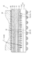
- FIG. 1 is a cross-sectional view showing a configuration example of an imaging device according to Embodiment 1 of the present disclosure.
- FIG. 2 is a cross-sectional view showing a configuration example of an integrated component according to Embodiment 1 of the present disclosure.
- FIG. 3A is a schematic diagram showing a configuration example of an integrated component.
- FIG. 3B is a schematic diagram illustrating a configuration example of an integrated component.
- FIG. 4 is a diagram illustrating a circuit configuration example of a solid-state imaging device according to Embodiment 1 of the present disclosure.
- FIG. 5 is a diagram illustrating an example of an equivalent circuit of a pixel according to Embodiment 1 of the present disclosure.
- FIG. 6 is a cross-sectional view showing an enlarged example of the detailed structure of the solid-state imaging device according to Embodiment 1 of the present disclosure.
- FIG. 7 is a cross-sectional view showing a configuration example of a pixel sensor substrate according to Embodiment 1 of the present disclosure.
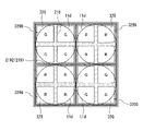
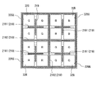
- 8A is a plan view showing Configuration Example 1 of a pixel layout according to Embodiment 1 of the present disclosure.
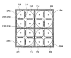
- FIG. 8B is a plan view showing an arrangement example of an on-chip lens with respect to the pixel layout shown in FIG. 8A.
- 9A is a plan view showing Configuration Example 2 of a pixel layout according to Embodiment 1 of the present disclosure.
- FIG. 9B is a plan view showing an arrangement example of an on-chip lens with respect to the pixel layout shown in FIG. 9A.
- 10A is a plan view showing Configuration Example 3 of a pixel layout according to Embodiment 1 of the present disclosure.
- FIG. 10B is a plan view showing an arrangement example of an on-chip lens with respect to the pixel layout shown in FIG. 10A.
- FIG. 11 is a plan view showing Modification 1 of Configuration Example 3 of the pixel layout.
- FIG. 12 is a plan view showing Modification 2 of Configuration Example 3 of the pixel layout.
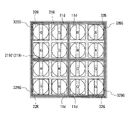
- 13A is a plan view showing Configuration Example 4 of a pixel layout according to Embodiment 1 of the present disclosure.
- FIG. 13B is a plan view showing an arrangement example of an on-chip lens with respect to the pixel layout shown in FIG. 13A.
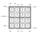
- FIG. 14 is a plan view showing Modification 1 of Configuration Example 4 of the pixel layout.
- FIG. 15 is a plan view showing Modification 2 of Configuration Example 4 of the pixel layout.
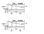
- FIG. 16 is a diagram showing a configuration example (No. 1) of the end portion of the WL lens 30.
- FIG. 17 is a diagram showing a configuration example (No. 2) of the end portion of the WL lens 30.
- FIG. 18 is a diagram showing a configuration example (part 3) of the end portion of the WL lens 30.
- FIG. 19 is a diagram showing a configuration example (No.
- FIG. 20 is a diagram illustrating a modification of the imaging device according to Embodiment 1 of the present disclosure.
- FIG. 21 is a diagram showing a configuration example (No. 1) of the concave lens 401.
- FIG. 22 is a diagram showing a configuration example (part 2) of the concave lens 401.
- FIG. 23 is a diagram showing a configuration example of a light shielding film arranged on the side surface of the concave lens 401 or the like.
- FIG. 24 is a cross-sectional view showing a configuration example of a pixel sensor substrate according to Embodiment 2 of the present disclosure.
- FIG. 25 is a block diagram showing a configuration example of an imaging device as an electronic device to which the present technology is applied.
- FIG. 26 is a diagram showing a usage example using the imaging device 1 described above.
- FIG. 27 is a diagram illustrating an example of a schematic configuration of an endoscopic surgery system to which technology (the present technology) according to the present disclosure can be applied.
- 28 is a block diagram showing an example of the functional configuration of the camera head and CCU shown in FIG. 27;
- FIG. FIG. 29 is a block diagram showing a schematic configuration example of a vehicle control system, which is an example of a mobile control system to which the technology according to the present disclosure can be applied.
- FIG. 30 is a diagram showing an example of the installation position of the imaging unit.
- planar view means, for example, viewing from the thickness direction of the silicon substrate 101 (that is, the direction normal to the front surface or the rear surface), which will be described later.
- + or - may be attached to p and n, which indicate the conductivity type of the semiconductor region.
- a semiconductor region marked with + or - means that the impurity concentration is relatively high or low, respectively, compared to a semiconductor region not marked with + or -.
- the semiconductor regions are given the same p and p (or the same n and n), it does not mean that the impurity concentration of each semiconductor region is exactly the same.
- FIG. 1 is a cross-sectional view showing a configuration example of an imaging device 1 according to Embodiment 1 of the present disclosure.
- the imaging device 1 in FIG. 1 includes a solid-state imaging device 11, a glass substrate 12, an IRCF (infrared light cut filter) 14, a wafer level lens 30, a lens group 16, a circuit board 17, an actuator 18 (a “holding unit” in the present disclosure). example), a connector 19, a spacer 20, and a wafer level lens 30 (hereinafter referred to as a WL lens; an example of a “concave lens” in the present disclosure).
- a WL lens an example of a “concave lens” in the present disclosure.
- the solid-state imaging device 11 is a so-called CMOS (Complementary Metal Oxide Semiconductor) or CCD (Charge Coupled). Device), etc., and is fixed on the circuit board 17 in an electrically connected state. As will be described later with reference to FIG. 4, the solid-state imaging device 11 is composed of a plurality of pixels arranged in an array. A pixel signal is generated according to the amount of incident light that is condensed and incident, and is output as an image signal from the connector 19 to the outside through the circuit board 17 .
- CMOS Complementary Metal Oxide Semiconductor
- CCD Charge Coupled. Device
- a glass substrate 12 is provided on the upper surface of the solid-state imaging device 11 in FIG.
- an IRCF 14 that cuts infrared light among incident light is provided.
- the IRCF 14 is attached to the upper surface of the glass substrate 12 with an adhesive (GLUE) 15 that is transparent and has substantially the same refractive index as the glass substrate 12 .
- the IRCF 14 is made of soda lime glass, for example, and cuts (removes) infrared light.
- the IRCF 14 also has substantially the same refractive index as the glass substrate 12 .
- a WL lens 30 is provided on the upper surface of the IRCF 14 in FIG.
- the WL lens 30 moderates the incident angle of incident light with respect to the light receiving surface of the pixel.
- the incident angle is the angle with respect to the vertical direction of the light receiving surface. Relaxing the incident angle means bringing the incident angle closer to 0°. When the incident angle is 0°, the incident light enters the light receiving surface perpendicularly.
- the WL lens 30 is a concave lens covering a plurality of pixels.
- the concave surface of the WL lens 30 faces the upper surface side in FIG. 1, that is, the lens group 16 side.
- the back surface (the back surface in FIG. 1) located on the opposite side of the concave surface of the WL lens 30 is adhered to the top surface of the IRCF 14 with an adhesive 25 .
- the WL lens 30 is transparent and made of glass having substantially the same refractive index as the glass substrate 12 .
- the WL lens 30 may be made of an organic material that is transparent and has substantially the same refractive index as the glass substrate 12 .
- the WL lens 30 is not limited to being colorless and transparent, and may be colored and transparent.
- the WL lens 30 is formed to have a diameter smaller than that of the IRCF 14 and the glass substrate 12 so as to cover all of the pixel region 21 (see, for example, FIGS. 3A and 3B) described later and not protrude from the IRCF 14 and the glass substrate 12. ing.
- the configuration of the WL lens 30 will be described in more detail in the column of configuration examples of the WL lens described later.
- the solid-state imaging device 11, the glass substrate 12, the IRCF 14, and the WL lens 30 are laminated and bonded with transparent adhesives 13, 15, and 25 to form an integral structure and connected to the circuit board 17. .
- the solid-state imaging device 11, the glass substrate 12, the IRCF 14, and the WL lens 30, which are surrounded by the dashed-dotted line in the drawing, are integrated by bonding with adhesives 13, 15, and 25 having substantially the same refractive index. Therefore, hereinafter, it is also simply referred to as an integrated component 10 .
- the IRCF 14 may be adhered onto the glass substrate 12 after being singulated in the manufacturing process of the solid-state imaging device 11, or may be a wafer-like glass substrate 12 composed of a plurality of solid-state imaging devices 11. After attaching the large-sized IRCF 14 to the entire upper surface, the solid-state imaging device 11 may be separated into individual pieces, or any method may be adopted. After attaching the IRCF 14, the WL lens 30 is attached.
- a spacer 20 is formed on the circuit board 17 so as to surround the solid-state imaging device 11, the glass substrate 12, the IRCF 14, and the WL lens 30 integrally constructed. Also, an actuator 18 is provided on the spacer 20 .
- the actuator 18 has a cylindrical shape and incorporates a lens group 16 formed by stacking a plurality of lenses inside the cylinder, and is driven vertically in FIG.
- the actuator 18 holds the lens group 16 and moves the held lens group 16 in the vertical direction in FIG.
- Autofocus is realized by adjusting the focus so as to form an image of the object on the imaging surface of the solid-state imaging device 11 according to the distance to the object (not shown).
- FIG. 2 is a cross-sectional view showing a configuration example of the integrated configuration section 10 according to Embodiment 1 of the present disclosure.
- the integrated component 10 shown in FIG. 2 is a semiconductor package in which a solid-state imaging device 11 is packaged, which is a laminated substrate formed by laminating a lower substrate 11a and an upper substrate 11b.
- a plurality of solder balls 11e which are back electrodes for electrical connection with the circuit board 17 of FIG.
- R (red), G (green), and B (blue) color filters 11c and an on-chip lens 11d are formed on the upper surface of the upper substrate 11b.
- the upper substrate 11b is connected to a glass substrate 12 for protecting the on-chip lens 11d via an adhesive 13 made of glass sealing resin in a cavityless structure.
- FIG. 3A and 3B are schematic diagrams showing configuration examples of the integrated configuration unit 10.
- the upper substrate 11b is provided with a pixel region 21 in which pixel portions for performing photoelectric conversion are two-dimensionally arranged in an array, and a control circuit 22 for controlling the pixel portions.
- a logic circuit 23 such as a signal processing circuit for processing pixel signals output from the pixel portion is formed on the lower substrate 11a.
- the control circuit 22 and the logic circuit 23 may be formed on the lower substrate 11a.
- the logic circuit 23 or both the control circuit 22 and the logic circuit 23 are formed on the lower substrate 11a different from the upper substrate 11b of the pixel region 21, and stacked on one semiconductor substrate. , the size of the imaging device 1 can be reduced as compared with the case where the pixel region 21, the control circuit 22 and the logic circuit 23 are arranged in the plane direction.
- the upper substrate 11b on which at least the pixel regions 21 are formed will be referred to as a pixel sensor substrate 11b
- the lower substrate 11a on which at least the logic circuit 23 will be formed will be referred to as a logic substrate 11a.
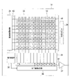
- FIG. 4 is a diagram showing a circuit configuration example of the solid-state imaging device 11 according to Embodiment 1 of the present disclosure.
- the solid-state imaging device 11 includes a pixel array section 33 in which pixels 32 are arranged in a two-dimensional array, a vertical drive circuit 34, a column signal processing circuit 35, a horizontal drive circuit 36, an output circuit 37, A control circuit 38 and an input/output terminal 39 are included.
- the pixel 32 has a photodiode as a photoelectric conversion element and a plurality of pixel transistors. A circuit configuration example of the pixel 32 will be described later with reference to FIG.
- the pixel 32 can have a shared pixel structure.
- This pixel-sharing structure is composed of a plurality of photodiodes, a plurality of transfer transistors, one shared floating diffusion (floating diffusion region), and one shared pixel transistor each. That is, in the shared pixel, the photodiodes and transfer transistors that constitute a plurality of unit pixels share another pixel transistor each.
- the control circuit 38 receives an input clock and data instructing the operation mode, etc., and outputs data such as internal information of the solid-state imaging device 11 . That is, the control circuit 38 generates clock signals and control signals that serve as references for the operation of the vertical drive circuit 34, the column signal processing circuit 35, the horizontal drive circuit 36, etc. based on the vertical synchronization signal, horizontal synchronization signal, and master clock. do. The control circuit 38 outputs the generated clock signal and control signal to the vertical drive circuit 34, the column signal processing circuit 35, the horizontal drive circuit 36, and the like.
- the vertical drive circuit 34 is composed of, for example, a shift register, selects a predetermined pixel drive wiring 40, supplies a pulse for driving the pixels 32 to the selected pixel drive wiring 40, and drives the pixels 32 row by row. do. That is, the vertical driving circuit 34 sequentially selectively scans the pixels 32 of the pixel array section 33 in the vertical direction on a row-by-row basis. is supplied to the column signal processing circuit 35 through the vertical signal line 41 .
- the column signal processing circuit 35 is arranged for each column of the pixels 32, and performs signal processing such as noise removal on the signals output from the pixels 32 of one row for each pixel column.
- the column signal processing circuit 5 performs signal processing such as CDS (Correlated Double Sampling) for removing pixel-specific fixed pattern noise and AD conversion.
- the horizontal driving circuit 36 is composed of, for example, a shift register, and sequentially outputs horizontal scanning pulses to select each of the column signal processing circuits 35 in turn, and outputs pixel signals from each of the column signal processing circuits 35 to the horizontal signal line. 42 to output.
- the output circuit 37 performs signal processing on the signals sequentially supplied from each of the column signal processing circuits 35 through the horizontal signal line 42 and outputs the processed signals.
- the output circuit 37 may perform only buffering, or may perform black level adjustment, column variation correction, various digital signal processing, and the like.
- the input/output terminal 39 exchanges signals with the outside.
- the solid-state imaging device 11 configured as described above is a CMOS image sensor called a column AD system in which a column signal processing circuit 35 for performing CDS processing and AD conversion processing is arranged for each pixel column.
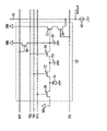
- FIG. 5 is a diagram showing an example of an equivalent circuit of the pixel 32 according to Embodiment 1 of the present disclosure.
- a pixel 32 shown in FIG. 5 shows a configuration for realizing an electronic global shutter function.
- the pixel 32 includes a photodiode 51 as a photoelectric conversion element, a first transfer transistor 52, a memory section (MEM) 53, a second transfer transistor 54, an FD (floating diffusion region) 55, a reset transistor 56, an amplification transistor 57, and a selection transistor. 58 , and an ejection transistor 59 .
- the photodiode 51 is a photoelectric conversion unit that generates and accumulates charges (signal charges) according to the amount of light received.
- the photodiode 51 has an anode terminal grounded and a cathode terminal connected to the memory section 53 via the first transfer transistor 52 .
- the cathode terminal of the photodiode 51 is also connected to a discharge transistor 59 for discharging unnecessary charges.
- the first transfer transistor 52 reads the charge generated by the photodiode 51 and transfers it to the memory section 53 when turned on by the transfer signal TRX.
- the memory unit 53 is a charge holding unit that temporarily holds charges until the charges are transferred to the FD 55 .
- the second transfer transistor 54 when turned on by the transfer signal TRG, reads the charge held in the memory section 53 and transfers it to the FD 55 .
- the FD 55 is a charge holding unit that holds charges read from the memory unit 53 for reading out as a signal.
- the reset transistor 56 is turned on by the reset signal RST, the charge accumulated in the FD 55 is discharged to the constant voltage source VDD, thereby resetting the potential of the FD 55 .
- the amplification transistor 57 outputs a pixel signal according to the potential of the FD55. That is, the amplification transistor 57 constitutes a source follower circuit together with a load MOS 60 as a constant current source, and a pixel signal indicating a level corresponding to the charge accumulated in the FD 55 is transmitted from the amplification transistor 57 through the selection transistor 58 to the column signal. It is output to the processing circuit 35 (FIG. 4).
- the load MOS 60 is arranged in the column signal processing circuit 35, for example.
- the selection transistor 58 is turned on when the pixel 32 is selected by the selection signal SEL, and outputs the pixel signal of the pixel 32 to the column signal processing circuit 35 via the vertical signal line 41 .
- the discharge transistor 59 discharges unnecessary charges accumulated in the photodiode 51 to the constant voltage source VDD when turned on by the discharge signal OFG.
- the transfer signals TRX and TRG, the reset signal RST, the ejection signal OFG, and the selection signal SEL are supplied from the vertical drive circuit 34 (FIG. 4) through the pixel drive wiring 40 (FIG. 4).
- a high-level discharge signal OFG is supplied to the discharge transistor 59 to turn on the discharge transistor 59, and the charge accumulated in the photodiode 51 is discharged to the constant voltage source VDD.
- photodiode 51 is reset. After the photodiode 51 is reset, when the discharge transistor 59 is turned off by the low-level discharge signal OFG, exposure of all pixels in the pixel array section 33 is started.
- the first transfer transistor 52 is turned on by the transfer signal TRX in all pixels of the pixel array section 33 , and the charge accumulated in the photodiode 51 is transferred to the memory section 53 . be done.
- the charges held in the memory section 53 of each pixel 32 are sequentially read out to the column signal processing circuit 35 row by row.
- the second transfer transistors 54 of the pixels 32 in the readout row are turned on by the transfer signal TRG, and the charges held in the memory section 53 are transferred to the FD55.
- the selection transistor 58 is turned on by the selection signal SEL, a signal indicating the level corresponding to the charge accumulated in the FD 55 is output from the amplification transistor 57 to the column signal processing circuit 35 via the selection transistor 58. be.
- the same exposure time is set for all the pixels in the pixel array section 33, and the charge is temporarily held in the memory section 53 after the end of the exposure.
- a global shutter type operation imaging in which charges are sequentially read out from the memory unit 53 in units of rows is possible. Note that the circuit configuration of the pixel 32 is not limited to the configuration shown in FIG.
- FIG. 6 is a cross-sectional view showing an enlarged example of the detailed structure of the solid-state imaging device 11 according to Embodiment 1 of the present disclosure.
- a multilayer wiring layer 82 is formed on the upper side (the pixel sensor substrate 11b side) of a semiconductor substrate 81 (hereinafter referred to as silicon substrate 81) made of silicon (Si), for example.
- the multilayer wiring layer 82 constitutes the control circuit 22 and the logic circuit 23 shown in FIGS. 3A and 3B.
- the multilayer wiring layer 82 includes a plurality of wiring layers 83 including a top wiring layer 83a closest to the pixel sensor substrate 11b, an intermediate wiring layer 83b, and a bottom wiring layer 83c closest to the silicon substrate 81, It is composed of an interlayer insulating film 84 formed between each wiring layer 83 .
- the plurality of wiring layers 83 are formed using, for example, copper (Cu), aluminum (Al), tungsten (W), or the like.
- the interlayer insulating film 84 is formed of, for example, a silicon oxide film, a silicon nitride film, or the like.
- Each of the plurality of wiring layers 83 and interlayer insulating films 84 may be formed of the same material in all layers, or two or more materials may be used depending on the layer.
- a silicon through hole 85 is formed through the silicon substrate 81 at a predetermined position of the silicon substrate 81 .
- a connection conductor 87 is embedded in the inner wall of the silicon through hole 85 via an insulating film 86 to form a through silicon via (TSV) 88 .
- the insulating film 86 can be formed of, for example, a SiO 2 film, a SiN film, or the like.
- the insulating film 86 and the connection conductor 87 are formed along the inner wall surface, and the inside of the silicon through hole 85 is hollow.
- the entire interior may be filled with connecting conductors 87 .
- the inside of the through-hole may be filled with a conductor or may be partially hollow. This also applies to a chip through electrode (TCV: Through Chip Via) 105 and the like, which will be described later.
- connection conductor 87 of the through-silicon electrode 88 is connected to the rewiring 90 formed on the lower surface side of the silicon substrate 81 .
- the rewiring 90 is connected to the solder balls 11e.
- the connection conductor 87 and the rewiring 90 can be made of, for example, copper (Cu), tungsten (W), tungsten (W), polysilicon, or the like.
- solder mask (solder resist) 91 is formed on the lower surface side of the silicon substrate 81 so as to cover the rewiring 90 and the insulating film 86 except for the regions where the solder balls 11e are formed.
- a multilayer wiring layer 102 is formed below (on the side of the logic substrate 11a) a semiconductor substrate 101 (hereinafter referred to as silicon substrate 101) made of silicon (Si).
- the multilayer wiring layer 102 constitutes the pixel circuit of the pixel region 21 shown in FIGS. 3A and 3B.
- the multilayer wiring layer 102 includes a plurality of wiring layers 103 including an uppermost wiring layer 103a closest to the silicon substrate 101, an intermediate wiring layer 103b, and a lowermost wiring layer 103c closest to the logic substrate 11a. It is composed of an interlayer insulating film 104 formed between wiring layers 103 .
- Materials used for the plurality of wiring layers 103 and the interlayer insulating film 104 can employ the same materials as those of the wiring layer 83 and the interlayer insulating film 84 described above. Further, the plurality of wiring layers 103 and interlayer insulating films 104 may be formed by selectively using one or more materials, as in the case of the wiring layers 83 and interlayer insulating films 84 described above.
- the multilayer wiring layer 102 of the pixel sensor substrate 11b is composed of three wiring layers 103, and the multilayer wiring layer 82 of the logic substrate 11a is composed of four wiring layers 83.
- the total number of wiring layers is not limited to this, and any number of layers can be formed.
- a photodiode 51 formed by a PN junction is formed for each pixel 32 in the silicon substrate 101 .
- a plurality of pixel transistors such as a first transfer transistor 52 and a second transfer transistor 54, a memory section (MEM) 53, and the like are also formed in the multilayer wiring layer 102 and the silicon substrate 101. ing.
- Silicon through electrodes 109 connected to the wiring layer 103a of the pixel sensor substrate 11b and the wiring layer 83a of the logic substrate 11a are provided at predetermined positions of the silicon substrate 101 where the color filter 11c and the on-chip lens 11d are not formed.
- a connected chip through electrode 105 is formed.
- the chip through electrode 105 and silicon through electrode 109 are connected by a connection wiring 106 formed on the upper surface of the silicon substrate 101 .
- An insulating film 107 is formed between each of the silicon through electrode 109 and the chip through electrode 105 and the silicon substrate 101 .
- a color filter 11c and an on-chip lens 11d are formed on the upper surface of the silicon substrate 101 with a planarizing film (insulating film) 108 interposed therebetween.
- the solid-state imaging device 11 shown in FIG. 2 has a laminated structure in which the multilayer wiring layer 102 side of the logic substrate 11a and the multilayer wiring layer 82 side of the pixel sensor substrate 11b are bonded together.
- a broken line indicates a bonding surface between the multilayer wiring layer 82 side of the logic substrate 11a and the multilayer wiring layer 102 side of the pixel sensor substrate 11b.
- the wiring layer 103 of the pixel sensor substrate 11b and the wiring layer 83 of the logic substrate 11a are connected by two through electrodes, ie, the silicon through electrode 109 and the chip through electrode 105.
- the wiring layer 83 of the substrate 11 a and the solder balls (rear electrodes) 11 e are connected by silicon through electrodes 88 and rewirings 90 .
- the plane area of the imaging device 1 can be minimized.
- the solid-state imaging device 11 and the glass substrate 12 can be made to have a cavityless structure and bonded together with an adhesive 13, so that the height can also be reduced.
- the imaging device 1 shown in FIG. 1 a more compact semiconductor device (semiconductor package) can be realized.
- the IRCF 14 is provided on the solid-state imaging element 11 and the glass substrate 12, so that it is possible to suppress the occurrence of flare and ghost due to the internal reflection of light. .
- FIG. 7 is a cross-sectional view showing a configuration example of the pixel sensor substrate 11b according to Embodiment 1 of the present disclosure.
- the pixel sensor substrate 11b of this embodiment includes a silicon substrate 101 having a plurality of pixels, a multilayer wiring layer 102 formed on the surface side of the silicon substrate 101, and a wiring layer 102 formed on the back surface side of the silicon substrate 101.
- the silicon substrate 101 has a thickness of 1 ⁇ m or more and 6 ⁇ m or less, for example.
- a plurality of pixels each composed of a photodiode 51 and a plurality of pixel transistors are formed in a two-dimensional matrix.
- the adjacent photodiodes 51 are electrically isolated by the inter-pixel isolation part 219 .
- the photodiode 51 is composed of p-type regions 223 and 224 formed on the front and back sides of the silicon substrate 101 and an n-type region 222 formed therebetween. A pn junction is formed between the p-type regions 223 and 224 and the n-type region 222 of the photodiode 51 .
- signal charges corresponding to the amount of incident light are generated and accumulated in the n-type region 222 .
- electrons that cause dark current generated at the interface of the silicon substrate 101 are absorbed by holes, which are majority carriers, in the p-type regions 223 and 224 formed on the front and back surfaces of the silicon substrate 101. Dark current is suppressed.
- Each photodiode 51 is electrically isolated by a p-type region 218 and an inter-pixel isolation portion 219 formed in the p-type region 218 .
- the FD 55 is composed of an n + -type region formed by ion-implanting n-type impurities at a high concentration into a p ⁇ well layer 229 formed on the surface side of the silicon substrate 101 .
- the transfer gate electrode 216 which is the gate electrode of the transfer transistor (for example, the first transfer transistor 52 or the second transfer transistor 54 shown in FIG. 5), is located on the silicon substrate 101 between the photodiode 51 and the FD 55. It is formed on the surface side with a gate insulating film 217 interposed therebetween.
- the inter-pixel isolation part 219 has a trench isolation structure.
- the inter-pixel isolation part 219 includes a trench 239 formed in the depth direction from the back surface side of the silicon substrate 101, a fixed charge film 220 formed so as to cover the inner side surface of the trench 239, and a fixed charge film 220. and an insulating film 221 (an example of a “filling film” in the present disclosure) embedded in the trench 239 via the .
- the inter-pixel isolation part 219 is formed by digging into the p-type region 218 formed in the silicon substrate 101 .
- the inter-pixel separation section 219 is formed, for example, in a lattice shape so as to surround the pixels. Further, when a pixel transistor is formed between adjacent photodiodes 51, the inter-pixel separating portion 219 is arranged so as to overlap the FD 55 and the source/drain regions of the pixel transistor in a plan view. It is
- the inter-pixel isolation portion 219 is formed to a depth reaching the p-well layer 29 in which the pixel transistor is formed, and not reaching the FD 55 and the source/drain regions. That is, the inter-pixel isolation part 219 is formed from the back surface (upper surface in FIG. 7) of the silicon substrate 101 to a midway position in the thickness direction of the silicon substrate 101 .
- the trench 239 that forms the inter-pixel isolation portion 219 opens on the back surface side of the silicon substrate 101 and has a bottom surface inside the silicon substrate 101 .
- the trench 239 is formed to a depth that does not reach the surface of the silicon substrate 101 .
- silicon substrate 101 has a thickness of 1 ⁇ m or more and 6 ⁇ m or less
- trench 239 is formed to a depth of 0.25 ⁇ m or more and 5.0 ⁇ m or less from the back surface of silicon substrate 101 .
- FIG. 7 shows the case where the inter-pixel isolation portion 219 is formed to a depth reaching the p-well layer 229, but the depth does not necessarily have to reach the p-well layer 229.
- the inter-pixel isolation part 219 may be formed so as to remain within the p-type region 218 without reaching the p-well layer 229 . Even if the inter-pixel isolation part 219 does not reach the p-well layer 229, the effect of isolation can be obtained.
- the fixed charge film 220 formed in the trench 239 is formed on the inner peripheral surface and the bottom surface of the trench 239 and is formed on the entire back surface of the silicon substrate 101 .
- the inner peripheral surface and the bottom surface of the trench 239 are collectively referred to as an "inner wall surface".
- the fixed charge film 220 it is preferable to use a material that can generate fixed charges and strengthen pinning by depositing on a substrate such as silicon. A dielectric film can be used.
- Specific materials for the fixed charge film 220 include, for example, oxides or nitrides containing at least one element selected from hafnium (Hf), aluminum (Al), zirconium (Zr), tantalum (Ta), and titanium (Ti). things can be applied.
- methods for forming the fixed charge film 220 include a chemical vapor deposition method (hereinafter referred to as a CVD (Chemical Vapor Deposition) method), a sputtering method, an atomic layer deposition method (hereinafter referred to as an ALD (Atomic Layer Deposition) method), and the like. mentioned.
- a SiO 2 film with a thickness of about 1 nm can be simultaneously formed to reduce the interface level during film formation.
- Other materials for the fixed charge film 220 include lanthanum (La), praseodymium (Pr), cerium (Ce), neodymium (Nd), promethium (Pm), samarium (Sm), europium (Eu), and gadolinium. (Gd), terbium (Tb), dysprosium (Dy), holmium (Ho), thulium (Tm), ytterbium (Yb), lutetium (Lu) and yttrium (Y). things, etc.
- the fixed charge film can be formed of a hafnium oxynitride film or an aluminum oxynitride film.
- Silicon (Si) or nitrogen (N) may be added to the material of the above-described fixed charge film 220 within a range that does not impair insulation.
- the concentration is appropriately determined within a range that does not impair the insulating properties of the film.
- the fixed charge film 220 having a negative charge is formed on the inner wall surface of the trench 239 and the back surface of the silicon substrate 101, an inversion layer is formed on the surface in contact with the fixed charge film 220.
- the silicon interface is pinned by the inversion layer, generation of dark current is suppressed.
- the fixed charge film 220 having many fixed charges is formed on the side walls and the bottom surface of the trench 239 to prevent pinning deviation.
- the insulating film 221 is embedded in the trench 239 in which the fixed charge film 220 is formed, and is formed on the entire rear surface side of the silicon substrate 101 .
- the insulating film 221 is preferably formed of a material having a refractive index different from that of the fixed charge film 220.
- silicon oxide, silicon nitride, silicon oxynitride, resin, or the like can be used.
- a material having no positive fixed charges or a small amount of positive fixed charges can be used for the insulating film 221 .
- the photodiodes 51 forming each pixel are separated through the insulating film 221 . This makes it difficult for signal charges to leak into adjacent pixels, so that when signal charges exceeding the saturation charge amount (Qs) are generated, overflowing signal charges can be reduced from leaking into the adjacent photodiodes 51. can be done. Therefore, electronic color mixture can be suppressed.
- Qs saturation charge amount
- the two-layer structure of the fixed charge film 220 and the insulating film 221 formed on the rear surface side of the silicon substrate 101, which is the incident surface side, has a role of an antireflection film due to the difference in refractive index. As a result, light incident from the back side of the silicon substrate 101 is prevented from being reflected on the back side of the silicon substrate 101 .
- the light-shielding film 225 is formed in a desired region on the insulating film 221 formed on the back surface of the silicon substrate 101, and is formed in a grid pattern so as to open the photodiodes 51 in the pixel region. That is, the light shielding film 225 is formed at a position corresponding to the inter-pixel separation portion 219 . The light shielding film 225 is formed at a position overlapping the inter-pixel separation portion 219 in plan view.
- the light shielding film 225 may be made of any material that blocks light, such as tungsten (W), aluminum (Al), or copper (Cu).
- the planarizing film 108 is formed on the entire surface of the insulating film 221 including the light shielding film 225, so that the back surface of the silicon substrate 101 is flattened.
- an organic material such as resin can be used as the material of the planarizing film 108.
- the color filters 11c are formed on the upper surface of the planarizing film 108, and are formed corresponding to, for example, R (red), G (green), and B (blue) for each pixel. Light of a desired wavelength is transmitted through the color filter 11 c , and the transmitted light is incident on the photodiode 51 in the silicon substrate 101 .
- the on-chip lens 11d is formed on the upper surface of the color filter 11c.
- the irradiated light is collected by the on-chip lens 11d, and the collected light efficiently enters each photodiode 51 via the color filter 11c.
- the pixel sensor substrate 11b having the above configuration, light is irradiated from the back surface (upper surface in FIG. 7) of the silicon substrate 101, and the light transmitted through the on-chip lens 11d and the color filter 11c is photoelectrically converted by the photodiode 51. By doing so, signal charges are generated.
- the signal charges generated by the photodiodes 51 are transmitted through the pixel transistors formed on the surface side of the silicon substrate 101 to the vertical signal lines 41 (see, for example, FIG. ) as a pixel signal.
- pixel layout Next, the layout of the pixel array section 33 of the solid-state imaging device 11 (hereinafter referred to as pixel layout) will be described.
- the pixel layout can adopt, for example, any one or more configurations of configuration examples 1 to 3 shown below.
- Configuration example 1 8A is a plan view showing Configuration Example 1 of a pixel layout according to Embodiment 1 of the present disclosure.
- FIG. FIG. 8B is a plan view showing an arrangement example of the on-chip lens 11d with respect to the pixel layout shown in FIG. 8A.
- the pixels 32 labeled G transmit green light (an example of the “first color” of the present disclosure) of the color filter 11c (see, for example, FIG. 7).
- green pixels 32G an example of a "first color pixel" of the present disclosure
- covered with a G filter an example of a "first color filter” of the present disclosure).
- the pixels 32 marked with R are R filters (an example of the “second color filter” of the present disclosure) that transmit red light (an example of the “second color” of the present disclosure) of the color filter 11c. , a red pixel 32R (an example of a "second color pixel” in this disclosure).
- the pixels 32 labeled B are B filters (an example of a “third color filter” of the present disclosure) that transmit blue light (an example of a “third color” of the present disclosure) of the color filter 11c. (an example of a "third color pixel" in this disclosure).
- the solid-state imaging device 11 includes, for example, a green pixel group 32GG (an example of the “first color pixel group” of the present disclosure) and a red pixel group 32RG (the “21st color pixel group” of the present disclosure). example) and a blue pixel group 32BG (an example of the “21st color pixel group” of the present disclosure).
- the green pixel group 32GG the green pixels 32G are arranged two by two in the horizontal direction (an example of the “first direction” of the present disclosure) and the vertical direction (an example of the “second direction” of the present disclosure) in plan view. has pixels.
- the red pixel group 32RG has four pixels in which the red pixels 32R are arranged two by two in the horizontal direction and the vertical direction in plan view.
- the blue pixel group 32BG has four pixels in which the blue pixels 32B are arranged two by two in the horizontal direction and the vertical direction in plan view.
- a unit layout is composed of the green pixel group 32GG, the red pixel group 32RG, and the blue pixel group 32BG.
- a pair of green pixel groups 32GG are arranged on a first diagonal line
- red pixel group 32RG and blue pixel group 32BG are arranged on a second diagonal line that intersects (for example, intersects) the first diagonal line.
- unit layout is configured.
- the pixel layout of the solid-state imaging device 11 has a configuration in which this unit layout is repeatedly arranged in the horizontal direction and the vertical direction in plan view. Accordingly, in the green pixel group 32GG, the red pixel group 32RG, and the blue pixel group 32BG, pixel groups of different colors are adjacent to each other in the horizontal direction and the vertical direction in plan view.
- one on-chip lens 11d is arranged for each four pixels arranged two by two in the horizontal direction and the vertical direction in plan view.
- one on-chip lens 11d is arranged in one green pixel group 32GG.
- One on-chip lens 11d is arranged in one red pixel group 32RG.
- One on-chip lens 11d is arranged in one blue pixel group 32BG.
- the inter-pixel separation section 219 has a same-color pixel separation section 2191 that separates adjacent pixels 32 of the same color, and a different-color pixel separation section 2192 that separates adjacent pixels 32 of a different color.
- a different-color pixel separation section 2192 that separates adjacent pixels 32 of a different color.
- Adjacent means adjoining horizontally or vertically in a plan view.
- the same-color pixel isolation portion 2191 and the different-color pixel isolation portion 2192 each have a trench isolation structure (for example, the structure of the pixel isolation portion 219 in FIG. 7, or , the structure of an inter-pixel separation portion 219A shown in FIG. 24 described later).
- the configuration example 1 of the pixel layout shown in FIGS. 8A and 8B can suppress color mixture between pixels of the same color and color mixture between pixels of different colors.
- pixels of different colors may be separated by an inter-pixel separation section having a trench isolation structure, and pixels of the same color may be separated by a diffusion layer.
- FIG. 9A is a plan view showing Configuration Example 2 of a pixel layout according to Embodiment 1 of the present disclosure.
- FIG. 9B is a plan view showing an arrangement example of an on-chip lens with respect to the pixel layout shown in FIG. 9A.
- the different-color pixel separation section 2192 has a trench isolation structure.
- the same-color pixel isolation portion 2191 is not of a trench isolation structure but is composed only of a p-type region 218, which is an example of a diffusion layer.
- adjacent green pixels 32G and red pixels 32R and adjacent green pixels 32G and blue pixels 32B are separated by different color pixel isolation portions 2192 having a trench isolation structure. Between one adjacent green pixel 32G and the other green pixel 32G, between one adjacent red pixel 32R and the other red pixel 32R, and between one adjacent blue pixel 32B and the other blue pixel 32B. are separated by the same-color pixel separating portion 2191 constituted by the p-type region 218 only.
- Configuration example 3 pixels of the same color may be partially separated by an inter-pixel separation section having a trench isolation structure in plan view.
- 10A is a plan view showing Configuration Example 3 of a pixel layout according to Embodiment 1 of the present disclosure.
- FIG. FIG. 10B is a plan view showing an arrangement example of the on-chip lens 11d with respect to the pixel layout shown in FIG. 10A.
- the different-color pixel separation section 2192 has a trench isolation structure.
- the same-color pixel isolation portion 2191 has a portion having a trench isolation structure and a portion composed only of the p-type region 218 .
- the same-color pixel isolation portion 2191 in each of the green pixel group 32GG, the red pixel group 32RG, and the blue pixel group 32BG is a trench isolation except for the outer periphery of each pixel group. have a structure.
- a same-color pixel separation portion 2191 in the outer peripheral portion of each pixel group is composed only of the p-type region 218 .
- the portion having the trench isolation structure in the same-color pixel isolation portion 2191 has a cross shape in plan view.
- the different-color pixel isolation portion 2192 has a trench isolation structure, it is possible to particularly suppress color mixture between different-color pixels.
- part of the same-color pixel separation section 2191 has a trench isolation structure, it is possible to suppress color mixture between the same-color pixels.
- the configuration example 3 described above may be a mode of a modification 1 shown in FIG. 11 or a mode of a modification 2 shown in FIG.
- FIG. 11 is a plan view showing Modification 1 of Configuration Example 3 of the pixel layout.
- a same-color pixel isolation portion having a trench isolation structure is provided between pixels of the same color in each of the green pixel group 32GG, the red pixel group 32RG, and the blue pixel group 32BG, except for the central portion of each pixel group. 2191 may be separated. The same-color pixels in the center of each pixel group may be separated by a same-color pixel separating portion 2191 composed only of the p-type region 218 .
- the shape of the same-color pixel separation portion 2191 having the trench isolation structure in a plan view is a straight line projecting from the periphery of each pixel group toward the center of each pixel group. Even in such a mode, color mixture between pixels of different colors and color mixture between pixels of the same color can be suppressed, as in configuration example 3 described above.
- FIG. 12 is a plan view showing Modification 2 of Configuration Example 3 of the pixel layout.
- trenches are provided between pixels of the same color in each of the green pixel group 32GG, the red pixel group 32RG, and the blue pixel group 32BG, except for the outer periphery of each pixel group and the true center of each pixel group. They may be separated by a same-color pixel separating portion 2191 having an isolation structure.
- the true central portion of the pixel group means, for example, an area closer to the center of the above-described pixel group.
- the same-color pixels in the outer periphery of each pixel group and the same-color pixels in the center of each pixel group may be separated by the same-color pixel separating portion 2191 composed only of the p-type region 218 .
- the shape of the same-color pixel isolation portion 2191 having the trench isolation structure in a plan view is a hollow cross shape. Even in such a mode, color mixture between pixels of different colors and color mixture between pixels of the same color can be suppressed, as in configuration example 3 described above.
- Configuration example 4 shows modes in which one on-chip lens 11d is arranged in one pixel group composed of four pixels.
- the placement of the on-chip lens 11d with respect to the pixel layout is not limited to this.
- one on-chip lens 11 d may be arranged in one pixel 32 .
- a diffusion layer may be provided in one pixel 32 in plan view.
- FIG. 13A is a plan view showing Configuration Example 4 of the pixel layout according to Embodiment 1 of the present disclosure.
- FIG. 13B is a plan view showing an arrangement example of the on-chip lens 11d with respect to the pixel layout shown in FIG. 13A.
- a p-type region 218 is provided within the pixel 32 .
- the p-type region 218 completely separates the inside of one pixel 32 into, for example, a left region and a right region.
- one on-chip lens 11 d is arranged for one pixel 32 .
- the different color pixels in each of the green pixel group 32GG, the red pixel group 32RG, and the blue pixel group 32BG are separated by the different color pixel separating portion 2192 having the trench isolation structure. Color mixing between different color pixels can be suppressed.
- the separation within the pixel 32 by the p-type region 218 may be partial in plan view. That is, configuration example 4 described above may be a mode of modification 1 shown in FIG. 14 or a mode of modification 2 shown in FIG. 15 below.
- FIG. 14 is a plan view showing Modification 1 of Configuration Example 4 of the pixel layout.
- the intra-pixel separation by the p-type region 218 is limited to the outer peripheral portion in plan view, and excludes the central portion.
- the p-type region 218 separates one pixel 32 into a left region and a right region, but this separation is not complete separation but partial separation.
- the p-type region 218 is not provided in the central portion of each pixel 32, and the left side region and the right side region are connected through this central portion. Even in such a mode, color mixture between pixels of different colors and color mixture between pixels of the same color can be suppressed, as in configuration example 4 described above.
- FIG. 15 is a plan view showing Modification 2 of Configuration Example 4 of the pixel layout.
- the p-type region 218 that partially separates each pixel 32 into the right region and the left region may be located on one side (for example, the upper side) of each pixel. Even in such a mode, color mixture between pixels of different colors and color mixture between pixels of the same color can be suppressed, as in configuration example 4 described above.
- the shape of the WL lens 30 in plan view may be circular, rectangular, or rectangular with rounded corners.
- the WL lens 30 is mounted on the solid-state imaging device 11 via the glass substrate 12, adhesive 15, IRCF 14, adhesive 25, and the like. Since the WL lens 30 is attached with an adhesive, the vicinity of the corners of the WL lens 30 tends to come off more easily than other portions. If the corners of the WL lens 30 are peeled off, incident light may not enter the solid-state imaging device 11 properly, resulting in flare or ghost.
- the outer dimensions of the WL lens 30 are set to values smaller than the outer dimensions of the solid-state imaging device 11, and the effective area is set near the center of the WL lens 30, while the outer circumference is ineffective.
- a region may be set. That is, the outer dimensions of the WL lens 30 are made smaller than the glass substrate 12 on the solid-state imaging device 11, and the non-effective area 30b is set on the outer periphery of the WL lens 30, and the effective area 30a is set inside thereof. make it As a result, it is possible to realize the WL lens 30 that is difficult to peel off from the solid-state imaging device 11, or that can effectively collect incident light even if the end portion is peeled off to some extent.
- the effective area 30a has an aspherical shape in the area of the WL lens 30 where the incident light is incident, and effectively functions to converge the incident light on the area of the solid-state imaging device 11 where photoelectric conversion is possible.
- the effective area 30a is a concentric structure formed with an aspherical lens structure, and is an area circumscribing the outer periphery of the lens. This is the area where light is condensed on the imaging surface.
- the non-effective area 30 b is an area that does not necessarily function as a lens that converges incident light that enters the WL lens 30 onto an area where the solid-state imaging device 11 photoelectrically converts the light.
- the non-effective area 30b it is desirable to extend the structure that functions as a partially aspherical lens at the boundary with the effective area 30a.
- the structure functioning as a lens is provided in the non-effective area 30b, extending near the boundary with the effective area 30a, so that the WL lens 30 is adhered to the glass substrate 12 on the solid-state imaging device 11. It is possible to appropriately collect incident light on the imaging surface of the solid-state imaging device 11 even if there is a positional deviation when the optical element is attached or attached.
- the end of the WL lens 30 is formed perpendicular to the imaging surface of the solid-state imaging device 11.
- the size of the WL lens 30 is set to be smaller than the size of the solid-state imaging device 11, the effective area 30a is set in the center of the WL lens 30, and the non-effective area is set in the outer periphery. If 30b is set, it may be formed in other shapes.
- FIG. 16 is a diagram showing a configuration example (part 1) of the end portion of the WL lens 30.
- FIG. As shown in the upper left part of FIG. 16, in the non-effective region 30b, at the boundary with the effective region 30a, a structure similar to that of the effective region 30a as an aspherical lens is extended to end Z331 of the non-effective region 30b. The ends may be formed vertically, as indicated by .
- ends may be tapered, as indicated by end Z332 of region 30b.
- ends may be rounded, as shown by end Z333 of region 30b.
- the end may be formed as a multi-tiered side surface.
- a structure similar to that of the effective region 30a as an aspherical lens is extended, and the edge of the non-effective region 30b is extended.
- a portion Z335 a bank-like protruding portion having a horizontal flat portion at the end portion and protruding in a direction opposite to the direction of incidence of incident light from the effective region 30a is formed, and then a protruding portion is formed.
- the sides of the portion may be formed vertically.
- the end has a flat portion in the horizontal direction, and a bank-like protruding portion that protrudes in the direction opposite to the incident direction of the incident light from the effective region 30a is formed. Additionally, the sides of the protrusion may be tapered.
- the end is provided with a flat portion in the horizontal direction, and a bank-like protruding portion protruding in the direction opposite to the incident direction of the incident light is formed from the effective area 30a.
- the side surface of the protrusion may be formed in a round shape.
- a structure similar to that of the effective region 30a as an aspherical lens is extended, and the edge of the non-effective region 30b is extended.
- a portion Z338 a bank-like protruding portion having a horizontal flat portion at the end and protruding in a direction opposite to the direction of incidence of incident light from the effective region 30a is formed.
- the side surface of the portion may be formed in a multi-stage structure.
- FIG. 16 shows a structural example in which the edge of the WL lens 30 is not provided with a bank-like projecting portion having a horizontal flat portion.
- the lower part of FIG. 16 shows a structural example in which the end of the WL lens 30 is provided with a protruding portion having a flat portion in the horizontal direction. 16 are, from left to right, an example in which the end of the WL lens 30 is perpendicular to the glass substrate 12, an example in which the end is tapered, and an example in which the end is tapered.
- An example of a round configuration and an example of a multistage configuration of side surfaces having a plurality of ends are shown.
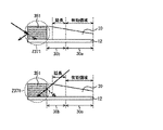
- FIG. 17 is a diagram showing a configuration example (No. 2) of the end portion of the WL lens 30.
- the non-effective region 30b at the boundary with the effective region 30a, the same structure as the effective region 30a as an aspherical lens is extended, and at the end Z351 of the non-effective region 30b
- the protruding portion is formed perpendicular to the glass substrate 12, and the solid-state imaging device 11 may be configured so as to leave a rectangular boundary structure Es at the boundary between the glass substrate 12 and the glass substrate 12. good.
- the projecting portion may be formed perpendicular to the glass substrate 12, and a round-shaped boundary structure Er may be left at the boundary between the solid-state imaging device 11 and the glass substrate 12. good.
- the WL lens 30 and the glass substrate 12 are brought into closer contact with each other by increasing the contact area between the WL lens 30 and the glass substrate 12. It is possible to bond them, and as a result, it is possible to suppress the separation of the WL lens 30 from the glass substrate 12 .
- the rectangular boundary structure Es and the round boundary structure Er are used when the end portion is formed in a tapered shape, in a round shape, or in a multi-stage structure. You may do so.
- FIG. 18 is a diagram showing a configuration example (part 3) of the end portion of the WL lens 30.
- FIG. 18 As shown in FIG. 18, in the non-effective region 30b, at the boundary with the effective region 30a, a structure similar to that of the effective region 30a as an aspherical lens is extended and indicated by an end Z371 of the non-effective region 30b. , the side surface of the WL lens 30 is formed perpendicular to the glass substrate 12, and a refractive film 351 having a predetermined refractive index is formed on the glass substrate 12 at the outer peripheral portion at approximately the same height as the WL lens 30. may be made.
- the refractive film 351 has a refractive index higher than a predetermined refractive index, and there is incident light from the outer peripheral portion of the WL lens 30 as indicated by the solid line arrows in the upper part of FIG. It reflects outside the WL lens 30 and reduces incident light on the sides of the WL lens 30 as indicated by the dashed arrows. As a result, stray light is suppressed from entering the WL lens 30, so flare and ghost are suppressed.
- WL lens 30 transmits light that would otherwise be transmitted outside the WL lens 30, and reduces reflected light from the side surfaces of the WL lens 30, as indicated by the dotted line arrow. As a result, stray light is suppressed from entering the WL lens 30, so that it is possible to suppress the occurrence of flare and ghost.
- FIG. 18 an example has been described in which the refractive film 351 is formed at the same height as the WL lens 30 on the glass substrate 12 and the edge is vertical.
- FIG. 19 is a diagram showing a configuration example (part 4) of the end portion of the WL lens 30.
- FIG. For example, as indicated by a region Z391 in the upper left part of FIG. You may make it the structure which had.
- the refraction film 351 has a tapered shape at the end and a thickness that is higher than the height of the end of the WL lens 30. As shown in FIG. In addition, it may be configured such that a part thereof covers the non-effective area 30 b of the WL lens 30 .
- the refractive film 351 may be configured to have a tapered shape from the height of the edge of the WL lens 30 to the edge of the glass substrate 12. good.
- the refraction film 351 is tapered at the edge of the glass substrate 12 and has a thickness lower than the height of the edge of the WL lens 30. may be configured with
- the refracting film 351 is recessed toward the glass substrate 12 from the height of the edge of the WL lens 30 and is formed in a round shape. may be configured.
- FIG. 20 is a diagram showing a modification of the imaging device 1 according to Embodiment 1 of the present disclosure.
- an aspherical concave lens 401 may be formed on the glass substrate 12 on the solid-state imaging device 11 concentrically around the center of gravity viewed from above. Also, the lens 401 has an AR coat (anti-reflection) 402 formed on the surface on which light is incident, and a projecting portion 401a is formed on the outer peripheral portion. Since the AR coat 402 suppresses the diffuse reflection of the reflected light from the solid-state imaging device 11, it is possible to suppress the occurrence of flare and ghost with higher accuracy.
- AR coat anti-reflection
- the AR coat 402 is a single-layer film or a multi-layer structure film, and includes, for example, transparent silicon-based resin, acrylic-based resin, epoxy-based resin, styrene-based resin, Si (silicon), C (carbon), H (hydrogen ) as a main component (e.g., SiCH, SiCOH, SiCNH), Si (silicon), N (nitrogen) as a main component, an insulating film (e.g., SiON, SiN), silicon hydroxide, alkylsilane, alkoxy
- a single-layer film such as a SiO2 film, a P--SiO film, or an HDP--SiO film formed using at least one material gas such as silane and polysiloxane and an oxidizing agent, or selected from these It is a multi-layer laminate containing one or more films.
- AR coating 402 can employ, for example, vacuum deposition, sputtering, or WET coating.
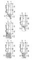
- FIG. 21 is a diagram showing a configuration example (part 1) of the concave lens 401.
- the lens 401 has a mortar-like shape with an aspheric concave shape centered on the center of gravity when viewed from above.
- the upper right part of the figure shows the cross-sectional shape of the lens 401 in the direction indicated by the dotted line in the upper left part of the figure
- the lower right part of the figure shows the cross-sectional shape of the upper left part of the figure.
- a cross-sectional shape of the lens 401 in the direction indicated by the solid line is shown.
- the range Ze of the lens 401 has a common aspheric curved surface structure in the upper right and lower right portions of FIG. form an effective area for condensing incident light.
- the thickness changes according to the distance from the center position in the direction of incidence of light and the direction perpendicular to it. More specifically, the lens thickness is the thinnest thickness D at the center position, and the lens thickness at the farthest position from the center in the range Ze is the thickest thickness H. Further, when the thickness of the glass substrate 12 is the thickness Th, the maximum thickness H of the lens 401 is thicker than the thickness Th of the glass substrate 12, and the minimum thickness D of the lens 401 is It is thinner than the thickness Th of the glass substrate 12 .
- the thicknesses D, H, and Th are achieved by using the lens 401 and the glass substrate 12 that satisfy the relationship of thickness H>thickness Th>thickness D.
- the imaging device 1 the integrated component 10 thereof capable of imaging at high resolution.
- the volume VG of the glass substrate 12 smaller than the volume VL of the lens 401, the volume of the lens can be formed most efficiently. It is possible to realize the imaging device 1 capable of imaging.
- the imaging device 1 that is compact and lightweight and capable of high-resolution imaging is provided by a concave lens 401 having a projecting portion 401a with a tapered outer peripheral portion, as shown in FIG.
- the lens 401 may have other shapes as long as the lens 401 and the glass substrate 12 have thicknesses D, H, and Th that satisfy the relationship of thickness H>thickness Th>thickness D. .
- the volumes VG and VL satisfy the relationship of volume VG ⁇ volume VL.
- FIG. 22 is a diagram showing a configuration example (part 2) of the concave lens 401.
- FIG. 22 the side surface on the outer peripheral side of the projecting portion 401a may be configured to form a right angle with respect to the glass substrate 12 and not include a taper.
- the side surface on the outer peripheral side of the projecting portion 401a may be configured to include a round taper.
- the protrusion 401a itself may not be included, and the side surface may include a straight tapered shape forming a predetermined angle with respect to the glass substrate 12. .
- the projection 401a itself may not be included, and the side surface may be configured to be perpendicular to the glass substrate 12 and not include the tapered shape.
- the side surface may be configured to include a round tapered shape with respect to the glass substrate 12 without including the projecting portion 401a itself.
- the side surface of the lens may have a two-stage structure having two inflection points without including the protruding portion 401a itself. Moreover, since the side surface of the lens 401L has a two-stage configuration with two points of inflection, it may be called a two-stage side surface type lens.
- the side surface may have a two-step structure including the projecting portion 401a and having two inflection points on the outer side surface.
- projection 401a is included, and the side surface is configured to be perpendicular to glass substrate 12, and furthermore, a rectangular skirting portion is provided near the boundary with glass substrate 12. 401b may be added.
- the projection 401a is included and formed at right angles to the glass substrate 12, and a round-shaped skirting portion 401b' is formed near the boundary with the glass substrate 12. You may make it add.
- a light shielding film may be formed so as to cover the projecting portion 401a and the side surface of the lens 401 to suppress the occurrence of side flare.
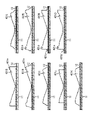
- FIG. 23 is a diagram showing a configuration example of the light shielding film 521 arranged on the side surface of the concave lens 401 or the like.
- the entire range up to the height of the flat portion of the side surface of the lens 401 and the upper surface of the protruding portion 401a, that is, the range other than the effective area is covered with the light shielding film. 521 may be formed.
- a membrane 521 may be formed.
- a light shielding film 521 may be formed on the side surface of the projecting portion 401a of the lens 401 from above the glass substrate 12 .
- the light shielding film 521 is formed in a range from the glass substrate 12 to a predetermined height on the side surface of the projecting portion 401a of the lens 401 from above the glass substrate 12.
- the light shielding film 521 may be formed only on the side surface of the projecting portion 401a of the lens 401.
- a light shielding film 521 may be formed in the range up to the highest positions of the two side surfaces of the two-step side-surface type lens 401 on the glass substrate 12 .
- a light shielding film 521 may be formed as shown in FIG.
- the light shielding film 521 may be formed by partial film formation, may be formed by lithography after film formation, or may be formed by forming a film after forming a resist and then lifting off the resist. good.
- the imaging device 1 includes the silicon substrate 101 (an example of the “semiconductor substrate” of the present disclosure) and the silicon substrate 101 provided on one surface of the silicon substrate 101 ( For example, a plurality of pixels 32 arranged side by side in a direction parallel to the rear surface); A color filter 11c provided on one surface side of the substrate 101, and a plurality of on-chips provided on one surface side of the silicon substrate 101 via the color filter 11c and arranged side by side in a direction parallel to the one surface. It includes a lens 11d and a WL lens 30 (or lens 401) provided on one side of the silicon substrate 101 via a color filter and a plurality of on-chip lenses 11d.
- the color filter 11c has a G filter that transmits green light, an R filter that transmits red light, and a B filter that transmits blue light.
- the multiple pixels 32 include green pixels 32G in which G filters are arranged, red pixels 32R in which R filters are arranged, and blue pixels 32B in which B filters are arranged.
- the inter-pixel separation section 219 includes a same-color pixel separation section 2191 arranged between adjacent same-color pixels 32 among the green pixel 32G, red pixel 32R, and blue pixel 32B, and a green pixel 32G, red pixel 32R, and blue pixel. 32B, a different-color pixel separating portion 2192 arranged between adjacent different-color pixels 32 is provided.
- the different color pixel separation section 2192 has a trench isolation structure.
- the WL lens 30 can moderate the incident angle of light incident on the pixels 32 on the high image height side (that is, the pixels 32 arranged at positions away from the center of the pixel region 21). , the incident angle on the high image height side can be brought close to 0° (that is, perpendicular to the back surface of the silicon substrate 101 which is the light receiving surface). Accordingly, color mixture between adjacent pixels can be suppressed on the high image height side. In addition, since adjacent pixels of different colors are separated by a trench isolation structure, color mixing can be further suppressed.
- At least a part (that is, part or all) of the same-color inter-pixel isolation part 2191 may have a trench isolation structure. According to this, not only adjacent pixels of different colors but also adjacent pixels of the same color are separated by the trench isolation structure, so color mixture can be further suppressed.
- the trench that constitutes the inter-pixel isolation section 219 opens on the back surface of the silicon substrate 101 (upper surface in FIG. 7) and extends into the silicon substrate 101. explained that it has In other words, it has been explained that the inter-pixel isolation part 219 is formed up to a midway position in the thickness direction of the silicon substrate 101 and does not penetrate the silicon substrate 101 .
- the trench forming the inter-pixel isolation part may penetrate between one surface (eg, back surface) of the semiconductor substrate and the other surface (eg, front surface) located on the opposite side of the one surface. . In other words, the inter-pixel separation portion may penetrate through the semiconductor substrate.
- FIG. 24 is a cross-sectional view showing a configuration example of a pixel sensor substrate 11b according to Embodiment 2 of the present disclosure.
- the pixel sensor substrate 11b according to the second embodiment is of the back-illuminated type, and the silicon substrate 101 is provided with a photodiode 51 and an inter-pixel isolation portion 219A surrounding the photodiode 51.
- the inter-pixel isolation part 219 has a trench isolation structure and penetrates the silicon substrate 101 .
- the inter-pixel isolation portion 219 includes a trench 239A provided in the p-type region 218, an insulating film 230 provided on the inner wall of the trench 239A, and a polysilicon film embedded in the trench 239A via the insulating film 230.
- 221A an example of a "filling membrane" of the present disclosure.
- the insulating film 230 is, for example, a silicon oxide film (SiO 2 film).
- Trench 239A penetrates between back surface 232 and front surface 233 of silicon substrate 101 . Thereby, the inter-pixel isolation part 219 penetrates the silicon substrate 101 .
- a p-type region 218 and an n-type region 231 are formed in order from the inter-pixel isolation portion 219A side toward the photodiode 51 . Also, p-type region 218 is in contact with back surface 232 of silicon substrate 101 , but n-type region 231 is not in contact with back surface 232 . A p-type region 224 is interposed between the n-type region 231 and the back surface 232 .
- the inter-pixel isolation part 219A SiN may be used as the insulating film 230 instead of the SiO 2 film.
- the insulating film 230 may be a fixed charge film, and as a specific material thereof, the same material as the above fixed charge film 220 (see FIG. 7, for example) can be used.
- Doping polysilicon may be used as the filling film instead of the polysilicon film 221A. When doped polysilicon is used as the filling film, or when the polysilicon film is formed and then doped with an n-type impurity or p-type impurity, a negative bias is applied to the filling film to form the inter-pixel isolation part. Since the pinning of the sidewalls of 219A can be strengthened, the dark characteristics can be further improved.
- the WL lens 30 can moderate the incident angle of light incident on the pixels 32 on the high image height side, and can bring the incident angle on the high image height side close to 0°. Accordingly, color mixture between adjacent pixels can be suppressed on the high image height side.
- the structure of the inter-pixel separation portion 219A penetrating the silicon substrate 101 is used for the different-color pixel separation portion 2192 (see FIGS. 8A to 15). Since adjacent pixels of different colors are separated by a trench isolation structure that penetrates the silicon substrate 101, color mixture can be further suppressed.
- the structure of the pixel isolation portion 219A penetrating through the silicon substrate 101 is used not only for the different color pixel isolation portion 2192 but also for at least a part of the same color pixel isolation portion 2191 (see FIGS. 8A to 15). good. As a result, not only adjacent pixels of different colors but also adjacent pixels of the same color are separated by the trench isolation structure penetrating the silicon substrate 101, so that color mixing can be further suppressed.
- the above-described imaging device 1 is an imaging device such as a digital still camera or a digital video camera, a mobile phone with an imaging function, or other equipment with an imaging function. It can be applied to equipment.
- FIG. 25 is a block diagram showing a configuration example of an imaging device as an electronic device to which this technology is applied.
- An imaging apparatus 1001 shown in FIG. 25 includes an optical system 1002, a shutter device 1003, a solid-state imaging device 1004, a driving circuit 1005, a signal processing circuit 1006, a monitor 1007, and a memory 1008, and captures still images and moving images. Imaging is possible.
- the optical system 1002 is configured with one or more lenses, guides light (incident light) from a subject to the solid-state imaging device 1004, and forms an image on the light-receiving surface of the solid-state imaging device 1004.
- the shutter device 1003 is arranged between the optical system 1002 and the solid-state imaging device 1004 and controls the light irradiation period and the light shielding period for the solid-state imaging device 1004 according to the control of the drive circuit 1005 .
- the solid-state image sensor 1004 is configured by a package including the solid-state image sensor described above.
- the solid-state imaging device 1004 accumulates signal charges for a certain period of time according to the light imaged on the light receiving surface via the optical system 1002 and shutter device 1003 .
- the signal charges accumulated in the solid-state imaging device 1004 are transferred according to the drive signal (timing signal) supplied from the drive circuit 1005 .
- a drive circuit 1005 drives the solid-state image sensor 1004 and the shutter device 1003 by outputting drive signals for controlling the transfer operation of the solid-state image sensor 1004 and the shutter operation of the shutter device 1003 .
- a signal processing circuit 1006 performs various signal processing on the signal charges output from the solid-state imaging device 1004 .
- An image (image data) obtained by the signal processing performed by the signal processing circuit 1006 is supplied to the monitor 1007 to be displayed, or supplied to the memory 1008 to be stored (recorded).
- the imaging apparatus 1001 configured in this way, by applying the imaging apparatus 1 in place of the optical system 1002 and the solid-state imaging device 1004 described above, it is possible to reduce the size and height of the apparatus configuration. , it is possible to suppress color mixture between adjacent pixels.
- FIG. 26 is a diagram showing a usage example using the imaging device 1 described above.
- the imaging device 1 described above can be used in various cases for sensing light such as visible light, infrared light, ultraviolet light, and X-rays as follows.
- ⁇ Devices that capture images for viewing purposes such as digital cameras and mobile devices with camera functions
- Devices used for transportation such as in-vehicle sensors that capture images behind, around, and inside the vehicle, surveillance cameras that monitor running vehicles and roads, and ranging sensors that measure the distance between vehicles.
- Devices used in home appliances such as TVs, refrigerators, air conditioners, etc., endoscopes, and devices that perform blood vessel imaging by receiving infrared light, etc.
- Equipment used for medical and health care ⁇ Equipment used for security purposes such as surveillance cameras for crime prevention and cameras for personal authentication ⁇ Skin measuring instruments for photographing the skin and photographing the scalp Equipment used for beauty, such as microscopes used for sports equipment Equipment used for sports, such as action cameras and wearable cameras for sports equipment Cameras for monitoring the condition of fields and crops, etc. , agricultural equipment
- the technology (the present technology) according to the present disclosure can be applied to various products.
- the technology according to the present disclosure may be applied to an endoscopic surgery system.
- FIG. 27 is a diagram showing an example of a schematic configuration of an endoscopic surgery system to which the technology according to the present disclosure (this technology) can be applied.
- FIG. 27 illustrates a state in which an operator (doctor) 11131 is performing surgery on a patient 11132 on a patient bed 11133 using an endoscopic surgery system 11000 .
- an endoscopic surgery system 11000 includes an endoscope 11100, other surgical instruments 11110 such as a pneumoperitoneum tube 11111 and an energy treatment instrument 11112, and a support arm device 11120 for supporting the endoscope 11100. , and a cart 11200 loaded with various devices for endoscopic surgery.
- An endoscope 11100 is composed of a lens barrel 11101 whose distal end is inserted into the body cavity of a patient 11132 and a camera head 11102 connected to the proximal end of the lens barrel 11101 .
- an endoscope 11100 configured as a so-called rigid scope having a rigid lens barrel 11101 is illustrated, but the endoscope 11100 may be configured as a so-called flexible scope having a flexible lens barrel. good.
- the tip of the lens barrel 11101 is provided with an opening into which the objective lens is fitted.
- a light source device 11203 is connected to the endoscope 11100, and light generated by the light source device 11203 is guided to the tip of the lens barrel 11101 by a light guide extending inside the lens barrel 11101, where it reaches the objective. Through the lens, the light is irradiated toward the observation object inside the body cavity of the patient 11132 .
- the endoscope 11100 may be a straight scope, a perspective scope, or a side scope.
- An optical system and an imaging element are provided inside the camera head 11102, and the reflected light (observation light) from the observation target is focused on the imaging element by the optical system.
- the imaging device photoelectrically converts the observation light to generate an electrical signal corresponding to the observation light, that is, an image signal corresponding to the observation image.
- the image signal is transmitted to a camera control unit (CCU: Camera Control Unit) 11201 as RAW data.
- CCU Camera Control Unit
- the CCU 11201 is composed of a CPU (Central Processing Unit), a GPU (Graphics Processing Unit), etc., and controls the operations of the endoscope 11100 and the display device 11202 in an integrated manner. Further, the CCU 11201 receives an image signal from the camera head 11102 and performs various image processing such as development processing (demosaicing) for displaying an image based on the image signal.
- CPU Central Processing Unit
- GPU Graphics Processing Unit
- the display device 11202 displays an image based on an image signal subjected to image processing by the CCU 11201 under the control of the CCU 11201 .
- the light source device 11203 is composed of a light source such as an LED (Light Emitting Diode), for example, and supplies the endoscope 11100 with irradiation light for photographing a surgical site or the like.
- a light source such as an LED (Light Emitting Diode), for example, and supplies the endoscope 11100 with irradiation light for photographing a surgical site or the like.
- the input device 11204 is an input interface for the endoscopic surgery system 11000.
- the user can input various information and instructions to the endoscopic surgery system 11000 via the input device 11204 .
- the user inputs an instruction or the like to change the imaging conditions (type of irradiation light, magnification, focal length, etc.) by the endoscope 11100 .
- the treatment instrument control device 11205 controls driving of the energy treatment instrument 11112 for tissue cauterization, incision, blood vessel sealing, or the like.
- the pneumoperitoneum device 11206 inflates the body cavity of the patient 11132 for the purpose of securing the visual field of the endoscope 11100 and securing the operator's working space, and injects gas into the body cavity through the pneumoperitoneum tube 11111. send in.
- the recorder 11207 is a device capable of recording various types of information regarding surgery.
- the printer 11208 is a device capable of printing various types of information regarding surgery in various formats such as text, images, and graphs.
- the light source device 11203 that supplies the endoscope 11100 with irradiation light for photographing the surgical site can be composed of, for example, a white light source composed of an LED, a laser light source, or a combination thereof.
- a white light source is configured by a combination of RGB laser light sources
- the output intensity and output timing of each color (each wavelength) can be controlled with high accuracy. It can be carried out.
- the observation target is irradiated with laser light from each of the RGB laser light sources in a time-division manner, and by controlling the drive of the imaging element of the camera head 11102 in synchronization with the irradiation timing, each of RGB can be handled. It is also possible to pick up images by time division. According to this method, a color image can be obtained without providing a color filter in the imaging device.
- the driving of the light source device 11203 may be controlled so as to change the intensity of the output light every predetermined time.
- the drive of the imaging device of the camera head 11102 in synchronism with the timing of the change in the intensity of the light to obtain an image in a time-division manner and synthesizing the images, a high dynamic A range of images can be generated.
- the light source device 11203 may be configured to be able to supply light in a predetermined wavelength band corresponding to special light observation.
- special light observation for example, the wavelength dependence of light absorption in body tissues is used to irradiate a narrower band of light than the irradiation light (i.e., white light) used during normal observation, thereby observing the mucosal surface layer.
- narrow band imaging in which a predetermined tissue such as a blood vessel is imaged with high contrast, is performed.
- fluorescence observation may be performed in which an image is obtained from fluorescence generated by irradiation with excitation light.
- the body tissue is irradiated with excitation light and the fluorescence from the body tissue is observed (autofluorescence observation), or a reagent such as indocyanine green (ICG) is locally injected into the body tissue and the body tissue is A fluorescence image can be obtained by irradiating excitation light corresponding to the fluorescence wavelength of the reagent.
- the light source device 11203 can be configured to be able to supply narrowband light and/or excitation light corresponding to such special light observation.
- FIG. 28 is a block diagram showing an example of functional configurations of the camera head 11102 and CCU 11201 shown in FIG.
- the camera head 11102 has a lens unit 11401, an imaging section 11402, a drive section 11403, a communication section 11404, and a camera head control section 11405.
- the CCU 11201 has a communication section 11411 , an image processing section 11412 and a control section 11413 .
- the camera head 11102 and the CCU 11201 are communicably connected to each other via a transmission cable 11400 .
- a lens unit 11401 is an optical system provided at a connection with the lens barrel 11101 . Observation light captured from the tip of the lens barrel 11101 is guided to the camera head 11102 and enters the lens unit 11401 .
- a lens unit 11401 is configured by combining a plurality of lenses including a zoom lens and a focus lens.
- the imaging unit 11402 is composed of an imaging element.
- the imaging device constituting the imaging unit 11402 may be one (so-called single-plate type) or plural (so-called multi-plate type).
- image signals corresponding to RGB may be generated by each image pickup element, and a color image may be obtained by synthesizing the image signals.
- the imaging unit 11402 may be configured to have a pair of imaging elements for respectively acquiring right-eye and left-eye image signals corresponding to 3D (Dimensional) display.
- the 3D display enables the operator 11131 to more accurately grasp the depth of the living tissue in the surgical site.
- a plurality of systems of lens units 11401 may be provided corresponding to each imaging element.
- the imaging unit 11402 does not necessarily have to be provided in the camera head 11102 .
- the imaging unit 11402 may be provided inside the lens barrel 11101 immediately after the objective lens.
- the drive unit 11403 is configured by an actuator, and moves the zoom lens and focus lens of the lens unit 11401 by a predetermined distance along the optical axis under control from the camera head control unit 11405 . Thereby, the magnification and focus of the image captured by the imaging unit 11402 can be appropriately adjusted.
- the communication unit 11404 is composed of a communication device for transmitting and receiving various information to and from the CCU 11201.
- the communication unit 11404 transmits the image signal obtained from the imaging unit 11402 as RAW data to the CCU 11201 via the transmission cable 11400 .
- the communication unit 11404 receives a control signal for controlling driving of the camera head 11102 from the CCU 11201 and supplies it to the camera head control unit 11405 .
- the control signal includes, for example, information to specify the frame rate of the captured image, information to specify the exposure value at the time of imaging, and/or information to specify the magnification and focus of the captured image. Contains information about conditions.
- the imaging conditions such as the frame rate, exposure value, magnification, and focus may be appropriately designated by the user, or may be automatically set by the control unit 11413 of the CCU 11201 based on the acquired image signal. good.
- the endoscope 11100 is equipped with so-called AE (Auto Exposure) function, AF (Auto Focus) function, and AWB (Auto White Balance) function.
- the camera head control unit 11405 controls driving of the camera head 11102 based on the control signal from the CCU 11201 received via the communication unit 11404.
- the communication unit 11411 is composed of a communication device for transmitting and receiving various information to and from the camera head 11102 .
- the communication unit 11411 receives image signals transmitted from the camera head 11102 via the transmission cable 11400 .
- the communication unit 11411 transmits a control signal for controlling driving of the camera head 11102 to the camera head 11102 .
- Image signals and control signals can be transmitted by electric communication, optical communication, or the like.
- the image processing unit 11412 performs various types of image processing on the image signal, which is RAW data transmitted from the camera head 11102 .
- the control unit 11413 performs various controls related to imaging of the surgical site and the like by the endoscope 11100 and display of the captured image obtained by imaging the surgical site and the like. For example, the control unit 11413 generates control signals for controlling driving of the camera head 11102 .
- control unit 11413 causes the display device 11202 to display a captured image showing the surgical site and the like based on the image signal that has undergone image processing by the image processing unit 11412 .
- the control unit 11413 may recognize various objects in the captured image using various image recognition techniques. For example, the control unit 11413 detects the shape, color, and the like of the edges of objects included in the captured image, thereby detecting surgical tools such as forceps, specific body parts, bleeding, mist during use of the energy treatment tool 11112, and the like. can recognize.
- the control unit 11413 may use the recognition result to display various types of surgical assistance information superimposed on the image of the surgical site. By superimposing and presenting the surgery support information to the operator 11131, the burden on the operator 11131 can be reduced and the operator 11131 can proceed with the surgery reliably.
- a transmission cable 11400 connecting the camera head 11102 and the CCU 11201 is an electrical signal cable compatible with electrical signal communication, an optical fiber compatible with optical communication, or a composite cable of these.
- wired communication is performed using the transmission cable 11400, but communication between the camera head 11102 and the CCU 11201 may be performed wirelessly.
- the technology according to the present disclosure can be applied to the endoscope 11100, the imaging unit 11402 of the camera head 11102, the image processing unit 11412 of the CCU 11201, etc. among the configurations described above.
- the imaging device 1 described above can be applied to the imaging unit 10402 .
- the imaging unit 11402 of the camera head 11102 the image processing unit 11412 of the CCU 11201, and the like, it is possible to obtain an operation site image with a lower latency. It is possible for the operator to perform treatment with the same feeling as when observing the surgical site by contact.
- the technology according to the present disclosure may also be applied to, for example, a microsurgery system.
- the technology (the present technology) according to the present disclosure can be applied to various products.
- the technology according to the present disclosure is implemented as a device mounted on any type of moving object such as automobiles, electric vehicles, hybrid electric vehicles, motorcycles, bicycles, personal mobility, airplanes, drones, ships, and robots. may
- FIG. 29 is a block diagram showing a schematic configuration example of a vehicle control system, which is an example of a mobile control system to which the technology according to the present disclosure can be applied.
- a vehicle control system 12000 includes a plurality of electronic control units connected via a communication network 12001.
- the vehicle control system 12000 includes a drive system control unit 12010, a body system control unit 12020, an outside information detection unit 12030, an inside information detection unit 12040, and an integrated control unit 12050.
- a microcomputer 12051, an audio/image output unit 12052, and an in-vehicle network I/F (interface) 12053 are illustrated.
- the drive system control unit 12010 controls the operation of devices related to the drive system of the vehicle according to various programs.
- the driving system control unit 12010 includes a driving force generator for generating driving force of the vehicle such as an internal combustion engine or a driving motor, a driving force transmission mechanism for transmitting the driving force to the wheels, and a steering angle of the vehicle. It functions as a control device such as a steering mechanism to adjust and a brake device to generate braking force of the vehicle.
- the body system control unit 12020 controls the operation of various devices equipped on the vehicle body according to various programs.
- the body system control unit 12020 functions as a keyless entry system, a smart key system, a power window device, or a control device for various lamps such as headlamps, back lamps, brake lamps, winkers or fog lamps.
- the body system control unit 12020 can receive radio waves transmitted from a portable device that substitutes for a key or signals from various switches.
- the body system control unit 12020 receives the input of these radio waves or signals and controls the door lock device, power window device, lamps, etc. of the vehicle.
- the vehicle exterior information detection unit 12030 detects information outside the vehicle in which the vehicle control system 12000 is installed.
- the vehicle exterior information detection unit 12030 is connected with an imaging section 12031 .
- the vehicle exterior information detection unit 12030 causes the imaging unit 12031 to capture an image of the exterior of the vehicle, and receives the captured image.
- the vehicle exterior information detection unit 12030 may perform object detection processing or distance detection processing such as people, vehicles, obstacles, signs, or characters on the road surface based on the received image.
- the imaging unit 12031 is an optical sensor that receives light and outputs an electrical signal according to the amount of received light.
- the imaging unit 12031 can output the electric signal as an image, and can also output it as distance measurement information.
- the light received by the imaging unit 12031 may be visible light or non-visible light such as infrared rays.
- the in-vehicle information detection unit 12040 detects in-vehicle information.
- the in-vehicle information detection unit 12040 is connected to, for example, a driver state detection section 12041 that detects the state of the driver.
- the driver state detection unit 12041 includes, for example, a camera that captures an image of the driver, and the in-vehicle information detection unit 12040 detects the degree of fatigue or concentration of the driver based on the detection information input from the driver state detection unit 12041. It may be calculated, or it may be determined whether the driver is dozing off.
- the microcomputer 12051 calculates control target values for the driving force generator, the steering mechanism, or the braking device based on the information inside and outside the vehicle acquired by the vehicle exterior information detection unit 12030 or the vehicle interior information detection unit 12040, and controls the drive system control unit.
- a control command can be output to 12010 .
- the microcomputer 12051 realizes the functions of ADAS (Advanced Driver Assistance System) including collision avoidance or shock mitigation, follow-up driving based on inter-vehicle distance, vehicle speed maintenance driving, vehicle collision warning, or vehicle lane deviation warning. Cooperative control can be performed for the purpose of ADAS (Advanced Driver Assistance System) including collision avoidance or shock mitigation, follow-up driving based on inter-vehicle distance, vehicle speed maintenance driving, vehicle collision warning, or vehicle lane deviation warning. Cooperative control can be performed for the purpose of ADAS (Advanced Driver Assistance System) including collision avoidance or shock mitigation, follow-up driving based on inter-vehicle distance, vehicle speed maintenance driving, vehicle collision warning, or vehicle
- the microcomputer 12051 controls the driving force generator, the steering mechanism, the braking device, etc. based on the information about the vehicle surroundings acquired by the vehicle exterior information detection unit 12030 or the vehicle interior information detection unit 12040, so that the driver's Cooperative control can be performed for the purpose of autonomous driving, etc., in which vehicles autonomously travel without depending on operation.
- the microcomputer 12051 can output a control command to the body system control unit 12020 based on the information outside the vehicle acquired by the information detection unit 12030 outside the vehicle.
- the microcomputer 12051 controls the headlamps according to the position of the preceding vehicle or the oncoming vehicle detected by the vehicle exterior information detection unit 12030, and performs cooperative control aimed at anti-glare such as switching from high beam to low beam. It can be carried out.
- the audio/image output unit 12052 transmits at least one of audio and/or image output signals to an output device capable of visually or audibly notifying the passengers of the vehicle or the outside of the vehicle.
- an audio speaker 12061, a display unit 12062, and an instrument panel 12063 are illustrated as output devices.
- the display unit 12062 may include at least one of an on-board display and a head-up display, for example.
- FIG. 30 is a diagram showing an example of the installation position of the imaging unit 12031.
- the vehicle 12100 has imaging units 12101, 12102, 12103, 12104, and 12105 as the imaging unit 12031.
- the imaging units 12101, 12102, 12103, 12104, and 12105 are provided at positions such as the front nose of the vehicle 12100, the side mirrors, the rear bumper, the back door, and the upper part of the windshield in the vehicle interior, for example.
- An image pickup unit 12101 provided in the front nose and an image pickup unit 12105 provided above the windshield in the passenger compartment mainly acquire images in front of the vehicle 12100 .
- Imaging units 12102 and 12103 provided in the side mirrors mainly acquire side images of the vehicle 12100 .
- An imaging unit 12104 provided in the rear bumper or back door mainly acquires an image behind the vehicle 12100 .
- Forward images acquired by the imaging units 12101 and 12105 are mainly used for detecting preceding vehicles, pedestrians, obstacles, traffic lights, traffic signs, lanes, and the like.
- FIG. 30 shows an example of the imaging range of the imaging units 12101 to 12104.
- the imaging range 12111 indicates the imaging range of the imaging unit 12101 provided in the front nose
- the imaging ranges 12112 and 12113 indicate the imaging ranges of the imaging units 12102 and 12103 provided in the side mirrors, respectively
- the imaging range 12114 The imaging range of an imaging unit 12104 provided on the rear bumper or back door is shown. For example, by superimposing the image data captured by the imaging units 12101 to 12104, a bird's-eye view image of the vehicle 12100 viewed from above can be obtained.
- At least one of the imaging units 12101 to 12104 may have a function of acquiring distance information.
- at least one of the imaging units 12101 to 12104 may be a stereo camera composed of a plurality of imaging elements, or may be an imaging element having pixels for phase difference detection.
- the microcomputer 12051 determines the distance to each three-dimensional object within the imaging ranges 12111 to 12114 and changes in this distance over time (relative velocity with respect to the vehicle 12100). , it is possible to extract, as the preceding vehicle, the closest three-dimensional object on the course of the vehicle 12100, which runs at a predetermined speed (for example, 0 km/h or more) in substantially the same direction as the vehicle 12100. can. Furthermore, the microcomputer 12051 can set the inter-vehicle distance to be secured in advance in front of the preceding vehicle, and perform automatic brake control (including following stop control) and automatic acceleration control (including following start control). In this way, cooperative control can be performed for the purpose of automatic driving in which the vehicle runs autonomously without relying on the operation of the driver.
- automatic brake control including following stop control
- automatic acceleration control including following start control
- the microcomputer 12051 converts three-dimensional object data related to three-dimensional objects to other three-dimensional objects such as motorcycles, ordinary vehicles, large vehicles, pedestrians, and utility poles. It can be classified and extracted and used for automatic avoidance of obstacles. For example, the microcomputer 12051 distinguishes obstacles around the vehicle 12100 into those that are visible to the driver of the vehicle 12100 and those that are difficult to see. Then, the microcomputer 12051 judges the collision risk indicating the degree of danger of collision with each obstacle, and when the collision risk is equal to or higher than the set value and there is a possibility of collision, an audio speaker 12061 and a display unit 12062 are displayed. By outputting an alarm to the driver via the drive system control unit 12010 and performing forced deceleration and avoidance steering via the drive system control unit 12010, driving support for collision avoidance can be performed.
- At least one of the imaging units 12101 to 12104 may be an infrared camera that detects infrared rays.
- the microcomputer 12051 can recognize a pedestrian by determining whether or not the pedestrian exists in the captured images of the imaging units 12101 to 12104 .
- recognition of a pedestrian is performed by, for example, a procedure for extracting feature points in images captured by the imaging units 12101 to 12104 as infrared cameras, and performing pattern matching processing on a series of feature points indicating the outline of an object to determine whether or not the pedestrian is a pedestrian.
- the audio image output unit 12052 outputs a rectangular outline for emphasis to the recognized pedestrian. is superimposed on the display unit 12062 . Also, the audio/image output unit 12052 may control the display unit 12062 to display an icon or the like indicating a pedestrian at a desired position.
- the technology according to the present disclosure can be applied to the imaging unit 12031 and the like among the configurations described above.
- the imaging device 1 described above can be applied to the imaging unit 12031 .
- FIGS. 1, 6, 7, and 24 show modes in which one on-chip lens 11d is arranged in one pixel 32, but this is only an example, and as shown in FIG.
- one on-chip lens 11d may be arranged for four pixels 32 in plan view, and one on-chip lens 11d may be arranged for two pixels 32 in cross-sectional view.
- the present disclosure can also take the following configurations.
- the plurality of pixels are a first color pixel in which a first color filter of the color filters is arranged; a second color pixel in which a second color filter of the color filters is arranged; a third color pixel in which a third color filter of the color filters is arranged;
- the inter-pixel separation unit a same-color pixel separating portion arranged between adjacent same-color pixels among
- the imaging device according to (1) wherein at least part of the same-color pixel separation section has the trench isolation structure.
- the trench isolation structure is a trench provided in the semiconductor substrate; and a filling film embedded in the trench.
- the trench is The imaging device according to (3) above, having an opening on the one surface side of the semiconductor substrate and having a bottom surface within the semiconductor substrate.
- the plurality of pixels are a first color pixel group having four pixels in which the first color pixels are arranged two by two in a first direction and in a second direction orthogonal to the first direction; a second color pixel group having four pixels in which the second color pixels are arranged two by two in the first direction and in the second direction; a third color pixel group having four pixels in which the third color pixels are arranged two pixels each in the first direction and the second direction; Any one of (1) to (5), wherein one convex lens is arranged in each of the first color pixel group, the second color pixel group, and the third color pixel group.
- Imaging device (8) a lens group arranged on the opposite side of the semiconductor substrate with the concave lens interposed therebetween and for allowing light to enter the concave lens;
Landscapes
- Engineering & Computer Science (AREA)
- Multimedia (AREA)
- Signal Processing (AREA)
- Solid State Image Pick-Up Elements (AREA)
- Transforming Light Signals Into Electric Signals (AREA)
- Color Television Image Signal Generators (AREA)
Abstract
Description
(撮像装置)
図1は、本開示の実施形態1に係る撮像装置1の構成例を示す断面図である。図1の撮像装置1は、固体撮像素子11、ガラス基板12、IRCF(赤外光カットフィルタ)14、ウェーハレベルレンズ30、レンズ群16、回路基板17、アクチュエータ18(本開示の「保持部」の一例)、コネクタ19、スペーサ20、ウェーハレベルレンズ30(以下、WLレンズ;本開示の「凹型レンズ」の一例)より構成されている。
Device)などからなるイメージセンサであり、回路基板17上で電気的に接続された状態で固定されている。固体撮像素子11は、図4を参照して後述するように、アレイ状に配置された複数の画素より構成され、画素単位で、図中上方よりレンズ群16と、WLレンズ30とを介して集光されて入射される、入射光の光量に応じた画素信号を生成し、画像信号として回路基板17を介してコネクタ19より外部に出力する。
次に、図2から図6を参照して、一体化構成部10の構成例につい説明する。図2は、本開示の実施形態1に係る一体化構成部10の構成例を示す断面図である。図2に示される一体化構成部10は、下側基板11aと上側基板11bとが積層されて構成されている積層基板からなる固体撮像素子11がパッケージ化された半導体パッケージである。
図4は、本開示の実施形態1に係る固体撮像素子11の回路構成例を示す図である。図4に示すように、固体撮像素子11は、画素32が2次元アレイ状に配列された画素アレイ部33と、垂直駆動回路34、カラム信号処理回路35、水平駆動回路36、出力回路37、制御回路38、及び入出力端子39を含む。
図5は、本開示の実施形態1に係る画素32の等価回路の一例を示す図である。図5に示される画素32は、電子式のグローバルシャッタ機能を実現する構成を示している。画素32は、光電変換素子としてのフォトダイオード51、第1転送トランジスタ52、メモリ部(MEM)53、第2転送トランジスタ54、FD(フローティング拡散領域)55、リセットトランジスタ56、増幅トランジスタ57、選択トランジスタ58、及び排出トランジスタ59を有する。
次に、固体撮像素子11の詳細構造の一例を説明する。図6は、本開示の実施形態1に係る固体撮像素子11の詳細構造の一例を拡大して示す断面図である。ロジック基板11aには、例えばシリコン(Si)で構成された半導体基板81(以下、シリコン基板81)の上側(画素センサ基板11b側)に、多層配線層82が形成されている。この多層配線層82により、図3A及び図3Bで示した制御回路22やロジック回路23が構成されている。
次に、本開示の実施形態1に係る画素センサ基板11bをより詳細に説明する。図7は、本開示の実施形態1に係る画素センサ基板11bの構成例を示す断面図である。
次に、固体撮像素子11の画素アレイ部33のレイアウト(以下、画素レイアウト)について説明する。本開示の実施形態において、画素レイアウトは、例えば、以下に示す構成例1から3のいずか1つ以上の構成を採ることができる。
図8Aは、本開示の実施形態1に係る画素レイアウトの構成例1を示す平面図である。図8Bは、図8Aに示す画素レイアウトに対する、オンチップレンズ11dの配置例を示す平面図である。なお、図8A及び図8Bにおいて、Gの符号が付された画素32は、カラーフィルタ11c(例えば、図7参照)のうち、緑色(本開示の「第1色」の一例)の光を透過するGフィルタ(本開示の「第1色フィルタ」の一例)で覆われた緑色画素32G(本開示の「第1色画素」の一例)である。Rの符号が付された画素32は、カラーフィルタ11cのうち、赤色(本開示の「第2色」の一例)の光を透過するRフィルタ(本開示の「第2色フィルタ」の一例)で覆われた赤色画素32R(本開示の「第2色画素」の一例)である。Bの符号が付された画素32は、カラーフィルタ11cのうち、青色(本開示の「第3色」の一例)の光を透過するBフィルタ(本開示の「第3色フィルタ」の一例)で覆われた青色画素32B(本開示の「第3色画素」の一例)である。
本開示の実施形態1において、画素レイアウトは、異色画素間がトレンチアイソレーション構造を有する画素間分離部で分離され、同色画素間は拡散層で分離されていてもよい。
本開示の実施形態では、同色画素間が、平面視で部分的に、トレンチアイソレーション構造を有する画素間分離部で分離されていてもよい。図10Aは、本開示の実施形態1に係る画素レイアウトの構成例3を示す平面図である。図10Bは、図10Aに示す画素レイアウトに対する、オンチップレンズ11dの配置例を示す平面図である。図10A及び図10Bに示すように、画素レイアウトの構成例3では、異色画素間分離部2192がトレンチアイソレーション構造を有する。同色画素間分離部2191は、トレンチアイソレーション構造を有する部分と、p型領域218のみで構成される部分とを有する。
上記の構成例1から3では、4つの画素で構成される1つの画素群に1つのオンチップレンズ11dが配置される態様を示した。しかしながら、本開示の実施形態において、画素レイアウトに対するオンチップレンズ11dの配置はこれに限定されない。本開示の実施形態では、1つの画素32に1つのオンチップレンズ11dが配置されていてもよい。また、平面視で、1つの画素32内に拡散層が設けられていてもよい。
WLレンズ30の平面視による形状は、円形状でもよいし、矩形状又は角丸矩形状であってもよい。図2に示したように、WLレンズ30は、ガラス基板12、接着剤15、IRCF14、接着剤25等を介して、固体撮像素子11上に取り付けられる。接着剤による取り付けのため、WLレンズ30の角部近傍は他の部分よりも剥がれ易い傾向がある。WLレンズ30の角部の剥がれが生じると、入射光が固体撮像素子11に適切に入射せず、フレアやゴーストが発生する可能性がる。
子11の光電変換可能な撮像面に集光する領域である。非有効領域30bとは、WLレンズ30に入射する入射光を、必ずしも、固体撮像素子11において光電変換される領域に集光するレンズとして機能しない領域である。
本開示の実施形態では、本開示の凹型レンズとして、WLレンズ30に代えて、以下で説明するレンズ401を用いてもよい。図20は、本開示の実施形態1に係る撮像装置1の変形例を示す図である。
以上説明したように、本開示の実施形態1に係る撮像装置1は、シリコン基板101(本開示の「半導体基板」の一例)と、シリコン基板101に設けられ、シリコン基板101の一方の面(例えば、裏面)に平行な方向に並んで配置される複数の画素32と、シリコン基板101に設けられ、複数の画素32のうちの隣り合う画素32間を分離する画素間分離部219と、シリコン基板101の一方の面側に設けられるカラーフィルタ11cと、カラーフィルタ11cを介してシリコン基板101の一方の面側に設けられ、一方の面に平行な方向に並んで配置される複数のオンチップレンズ11dと、カラーフィルタ及び複数のオンチップレンズ11dを介してシリコン基板101の一方の面側に設けられたWLレンズ30(または、レンズ401)と、を備える。
上記の実施形態1では、図7に示したように、画素間分離部219を構成するトレンチが、シリコン基板101の裏面(図7では、上面)に開口し、かつシリコン基板101内に底面を有することを説明した。つまり、画素間分離部219は、シリコン基板101の厚さ方向における途中の位置まで形成されており、シリコン基板101を貫通していないことを説明した。しかしながら、本開示の実施形態はこれに限定されない。画素間分離部を構成するトレンチは、半導体基板の一方の面(例えば、裏面)と、一方の面の反対側に位置する他方の面(例えば、表面)との間を貫通していてもよい。つまり、画素間分離部は、半導体基板を貫通していてもよい。
図15参照)の少なくとも一部についても、シリコン基板101を貫通する画素間分離部219Aの構造が用いられてよい。これにより、隣接する異色画素間だけでなく、隣接する同色画素間も、シリコン基板101を貫通するトレンチアイソレーション構造で分離されるため、混色をさらに抑制することができる。
上述した撮像装置1(例えば、図1参照)は、例えば、デジタルスチルカメラやデジタルビデオカメラなどの撮像装置、撮像機能を備えた携帯電話機、または、撮像機能を備えた他の機器といった各種の電子機器に適用することができる。
図26は、上述の撮像装置1を使用する使用例を示す図である。上述した撮像装置1は、例えば、以下のように、可視光や、赤外光、紫外光、X線等の光をセンシングする様々なケースに使用することができる。
・ディジタルカメラや、カメラ機能付きの携帯機器等の、鑑賞の用に供される画像を撮影する装置
・自動停止等の安全運転や、運転者の状態の認識等のために、自動車の前方や後方、周囲、車内等を撮影する車載用センサ、走行車両や道路を監視する監視カメラ、車両間等の測距を行う測距センサ等の、交通の用に供される装置
・ユーザのジェスチャを撮影して、そのジェスチャに従った機器操作を行うために、TVや、冷蔵庫、エアーコンディショナ等の家電に供される装置
・内視鏡や、赤外光の受光による血管撮影を行う装置等の、医療やヘルスケアの用に供される装置
・防犯用途の監視カメラや、人物認証用途のカメラ等の、セキュリティの用に供される装置
・肌を撮影する肌測定器や、頭皮を撮影するマイクロスコープ等の、美容の用に供される装置
・スポーツ用途等向けのアクションカメラやウェアラブルカメラ等の、スポーツの用に供される装置
・畑や作物の状態を監視するためのカメラ等の、農業の用に供される装置
本開示に係る技術(本技術)は、様々な製品へ応用することができる。例えば、本開示に係る技術は、内視鏡手術システムに適用されてもよい。
本開示に係る技術(本技術)は、様々な製品へ応用することができる。例えば、本開示に係る技術は、自動車、電気自動車、ハイブリッド電気自動車、自動二輪車、自転車、パーソナルモビリティ、飛行機、ドローン、船舶、ロボット等のいずれかの種類の移動体に搭載される装置として実現されてもよい。
上記のように、本開示は実施形態及び変形例によって記載したが、この開示の一部をなす論述及び図面は本開示を限定するものであると理解すべきではない。この開示から当業
者には様々な代替実施の形態、実施例及び運用技術が明らかとなろう。例えば、図1及び図2に示した一体化構成部10において、ガラス基板12及びIRCF14の少なくとも一方を、必要に応じて省略してもよい。また、図2、図6、図7、図24では、1つの画素32に1つのオンチップレンズ11dが配置される態様を示したが、これはあくまで一例であり、図8B等に示したように、平面視で4つの画素32に1つのオンチップレンズ11dが配置されていてもよく、断面視では2つの画素32に1つのオンチップレンズ11dが配置されていてもよい。
(1)
半導体基板と、
前記半導体基板に設けられ、前記半導体基板の一方の面に平行な方向に並んで配置される複数の画素と、
前記半導体基板に設けられ、複数の画素のうちの隣り合う画素間を分離する画素間分離部と、
前記半導体基板の前記一方の面側に設けられるカラーフィルタと、
前記カラーフィルタを介して前記半導体基板の前記一方の面側に設けられ、前記一方の面に平行な方向に並んで配置される複数の凸型レンズと、
前記カラーフィルタ及び前記複数の凸型レンズを介して前記半導体基板の前記一方の面側に設けられた凹型レンズと、を備え、
前記複数の画素は、
前記カラーフィルタのうちの第1色フィルタが配置される第1色画素と、
前記カラーフィルタのうちの第2色フィルタが配置される第2色画素と、
前記カラーフィルタのうちの第3色フィルタが配置される第3色画素と、を有し、
前記画素間分離部は、
前記第1色画素、前記第2色画素及び前記第3色画素のうち、隣接する同色の画素間に配置される同色画素間分離部と、
前記第1色画素、前記第2色画素及び前記第3色画素のうち、隣接する異色の画素間に配置される異色画素間分離部と、を有し、
前記異色画素間分離部は、トレンチアイソレーション構造を有する、撮像装置。
(2)
前記同色画素間分離部の少なくとも一部は、前記トレンチアイソレーション構造を有する、前記(1)に記載の撮像装置。
(3)
前記トレンチアイソレーション構造は、
前記半導体基板に設けられたトレンチと、
前記トレンチに埋め込まれた充填膜と、を有する前記(1)又は(2)に記載の撮像装置。
(4)
前記トレンチは、
前記半導体基板の前記一方の面側に開口し、かつ前記半導体基板内に底面を有する、前記(3)に記載に撮像装置。
(5)
前記トレンチは、前記半導体基板の前記一方の面と、前記一方の面の反対側に位置する他方の面との間を貫通する、前記(3)に記載の撮像装置。
(6)
前記複数の画素は、
前記第1色画素が第1方向と、前記第1方向と直交する第2方向とに2画素ずつ並べられた4画素を有する第1色画素群と、
前記第2色画素が前記第1方向と前記第2方向とに2画素ずつ並べられた4画素を有する第2色画素群と、
前記第3色画素が前記第1方向と前記第2方向とに2画素ずつ並べられた4画素を有する第3色画素群と、を有し、
前記第1色画素群、前記第2色画素群及び前記第3色画素群にそれぞれ、前記凸型レンズが1つずつ配置されている、前記(1)から(5)のいずれか1項に記載の撮像装置。(7)
前記第1色画素群、前記第2色画素群及び前記第3色画素群は、前記第1方向及び前記第2方向で異色の画素群同士が隣接している、前記(6)に記載の撮像装置。
(8)
前記凹型レンズを挟んで前記半導体基板の反対側に配置され、前記凹型レンズに光を入射させるレンズ群と、
前記レンズ群を保持する保持部と、をさらに備える前記(1)から(7)のいずれか1項に記載の撮像装置。
5 カラム信号処理回路
10 一体化構成部
11、1004 固体撮像素子
11a 下側基板(ロジック基板)
11b 上側基板(画素センサ基板)
11c カラーフィルタ
11d オンチップレンズ
11e ボール(裏面電極)
11e ボール
12 ガラス基板
13、15、25 接着剤
16 レンズ群
17 回路基板
18 アクチュエータ
19 コネクタ
20 スペーサ
21 画素領域
22 制御回路
23 ロジック回路
29 ウェル層
30 ウェーハレベルレンズ(WLレンズ)
30a 有効領域
30b 非有効領域
32 画素
32B 青色画素
32BG 青色画素群
32G 緑色画素
32GG 緑色画素群
32R 赤色画素
32RG 赤色画素群
33 画素アレイ部
34 垂直駆動回路
35 カラム信号処理回路
36 水平駆動回路
37 出力回路
38 制御回路
39 入出力端子
40 画素駆動配線
41 垂直信号線
42 水平信号線
51 フォトダイオード
52 第1転送トランジスタ
53 メモリ部
54 第2転送トランジスタ
56 リセットトランジスタ
57 増幅トランジスタ
58 選択トランジスタ
59 排出トランジスタ
81、101 半導体基板(シリコン基板)
82、102 多層配線層
83、103、103a、103b、103c 配線層
83a、83b、83c 配線層
84、104 層間絶縁膜
85 シリコン貫通孔
86、107、221、230 絶縁膜
87 接続導体
88、109 シリコン貫通電極
90 再配線
91 ソルダマスク(ソルダレジスト)
105 チップ貫通電極
106 接続用配線
108 平坦化膜(絶縁膜)
216 転送ゲート電極
217 ゲート絶縁膜
218、223、224 p型領域
219、219A 画素間分離部
220 絶縁膜(固定電荷膜)
221A ポリシリコン膜
222、231 n型領域
225、521 遮光膜
229 ウェル層
232 裏面
233 表面
239、239A トレンチ
351 屈折膜
401、401G、401H、401I、401J、401K、401L、401M、401N レンズ
401a 突出部
401b、401b´ 裾引き部
402 ARコート
1002 光学系
1003 シャッタ装置
1005 駆動回路
1006 信号処理回路
1007 モニタ
1008 メモリ
2191 同色画素間分離部
2192 異色画素間分離部
10402 撮像部
11000 内視鏡手術システム
11100 内視鏡
11101 鏡筒
11102 カメラヘッド
11110 術具
11111 気腹チューブ
11112 エネルギー処置具
11120 支持アーム装置
11131 術者(医師)
11132 患者
11133 患者ベッド
11200 カート
11201 カメラコントロールユニット
11202 表示装置
11203 光源装置
11204 入力装置
11205 処置具制御装置
11206 気腹装置
11207 レコーダ
11208 プリンタ
11400 伝送ケーブル
11401 レンズユニット
11402 撮像部
11403 駆動部
11404 通信部
11405 カメラヘッド制御部
11411 通信部
11412 画像処理部
11413 制御部
12000 車両制御システム
12001 通信ネットワーク
12010 駆動系制御ユニット
12020 ボディ系制御ユニット
12030 車外情報検出ユニット
12031 撮像部
12040 車内情報検出ユニット
12041 運転者状態検出部
12050 統合制御ユニット
12051 マイクロコンピュータ
12052 音声画像出力部
12061 オーディオスピーカ
12062 表示部
12063 インストルメントパネル
12100 車両
12101、12102、12103、12104、12105 撮像部
12111、12112、12113、12114 撮像範囲
CCU11201 撮像部
Er、Es 境界構造
FD 第2転送トランジスタ
I 車載ネットワーク
ICG インドシアニングリーン
OFG 排出信号
Qs 飽和電荷量
RST リセット信号
SEL 選択信号
TRG、TRX 転送信号
VDD 定電圧源
Z331、Z332、Z333、Z334、Z335、Z336、Z337、Z338、Z351、Z352、Z371 端部
Z391、Z392、Z393、Z394、Z395 領域
Ze 範囲
Claims (8)
- 半導体基板と、
前記半導体基板に設けられ、前記半導体基板の一方の面に平行な方向に並んで配置される複数の画素と、
前記半導体基板に設けられ、複数の画素のうちの隣り合う画素間を分離する画素間分離部と、
前記半導体基板の前記一方の面側に設けられるカラーフィルタと、
前記カラーフィルタを介して前記半導体基板の前記一方の面側に設けられ、前記一方の面に平行な方向に並んで配置される複数の凸型レンズと、
前記カラーフィルタ及び前記複数の凸型レンズを介して前記半導体基板の前記一方の面側に設けられた凹型レンズと、を備え、
前記複数の画素は、
前記カラーフィルタのうちの第1色フィルタが配置される第1色画素と、
前記カラーフィルタのうちの第2色フィルタが配置される第2色画素と、
前記カラーフィルタのうちの第3色フィルタが配置される第3色画素と、を有し、
前記画素間分離部は、
前記第1色画素、前記第2色画素及び前記第3色画素のうち、隣接する同色の画素間に配置される同色画素間分離部と、
前記第1色画素、前記第2色画素及び前記第3色画素のうち、隣接する異色の画素間に配置される異色画素間分離部と、を有し、
前記異色画素間分離部は、トレンチアイソレーション構造を有する、撮像装置。 - 前記同色画素間分離部の少なくとも一部は、前記トレンチアイソレーション構造を有する、請求項1に記載の撮像装置。
- 前記トレンチアイソレーション構造は、
前記半導体基板に設けられたトレンチと、
前記トレンチに埋め込まれた充填膜と、を有する請求項1に記載の撮像装置。 - 前記トレンチは、
前記半導体基板の前記一方の面側に開口し、かつ前記半導体基板内に底面を有する、請求項3に記載の撮像装置。 - 前記トレンチは、前記半導体基板の前記一方の面と、前記一方の面の反対側に位置する他方の面との間を貫通する、請求項3に記載の撮像装置。
- 前記複数の画素は、
前記第1色画素が第1方向と、前記第1方向と直交する第2方向とに2画素ずつ並べられた4画素を有する第1色画素群と、
前記第2色画素が前記第1方向と前記第2方向とに2画素ずつ並べられた4画素を有する第2色画素群と、
前記第3色画素が前記第1方向と前記第2方向とに2画素ずつ並べられた4画素を有する第3色画素群と、を有し、
前記第1色画素群、前記第2色画素群及び前記第3色画素群にそれぞれ、前記凸型レンズが1つずつ配置されている、請求項1に記載の撮像装置。 - 前記第1色画素群、前記第2色画素群及び前記第3色画素群は、前記第1方向及び前記第2方向で異色の画素群同士が隣接している、請求項6に記載の撮像装置。
- 前記凹型レンズを挟んで前記半導体基板の反対側に配置され、前記凹型レンズに光を入射させるレンズ群と、
前記レンズ群を保持する保持部と、をさらに備える請求項1に記載の撮像装置。
Priority Applications (1)
| Application Number | Priority Date | Filing Date | Title |
|---|---|---|---|
| US18/261,685 US12538600B2 (en) | 2021-01-26 | 2021-12-28 | Imaging device |
Applications Claiming Priority (2)
| Application Number | Priority Date | Filing Date | Title |
|---|---|---|---|
| JP2021-010690 | 2021-01-26 | ||
| JP2021010690A JP2022114386A (ja) | 2021-01-26 | 2021-01-26 | 撮像装置 |
Publications (1)
| Publication Number | Publication Date |
|---|---|
| WO2022163296A1 true WO2022163296A1 (ja) | 2022-08-04 |
Family
ID=82654617
Family Applications (1)
| Application Number | Title | Priority Date | Filing Date |
|---|---|---|---|
| PCT/JP2021/048888 Ceased WO2022163296A1 (ja) | 2021-01-26 | 2021-12-28 | 撮像装置 |
Country Status (3)
| Country | Link |
|---|---|
| US (1) | US12538600B2 (ja) |
| JP (1) | JP2022114386A (ja) |
| WO (1) | WO2022163296A1 (ja) |
Cited By (2)
| Publication number | Priority date | Publication date | Assignee | Title |
|---|---|---|---|---|
| WO2024057724A1 (ja) * | 2022-09-15 | 2024-03-21 | ソニーセミコンダクタソリューションズ株式会社 | 撮像装置、及び電子機器 |
| WO2025032961A1 (ja) * | 2023-08-07 | 2025-02-13 | ソニーセミコンダクタソリューションズ株式会社 | 光検出装置及び電子機器 |
Families Citing this family (4)
| Publication number | Priority date | Publication date | Assignee | Title |
|---|---|---|---|---|
| US12557411B2 (en) * | 2020-05-28 | 2026-02-17 | Sony Semiconductor Solutions Corporation | Solid-state imaging device and electronic apparatus |
| WO2024106196A1 (ja) * | 2022-11-16 | 2024-05-23 | ソニーセミコンダクタソリューションズ株式会社 | 固体撮像装置および電子機器 |
| WO2024154590A1 (ja) * | 2023-01-18 | 2024-07-25 | ソニーセミコンダクタソリューションズ株式会社 | 光検出装置 |
| TW202443879A (zh) * | 2023-04-10 | 2024-11-01 | 日商索尼半導體解決方案公司 | 光檢測元件 |
Citations (5)
| Publication number | Priority date | Publication date | Assignee | Title |
|---|---|---|---|---|
| JP2012114479A (ja) * | 2012-03-19 | 2012-06-14 | Toshiba Corp | 固体撮像装置 |
| JP2016139988A (ja) * | 2015-01-28 | 2016-08-04 | 株式会社東芝 | 固体撮像装置 |
| JP2018201015A (ja) * | 2017-05-29 | 2018-12-20 | ソニーセミコンダクタソリューションズ株式会社 | 固体撮像装置、及び電子機器 |
| JP2020031127A (ja) * | 2018-08-22 | 2020-02-27 | ソニーセミコンダクタソリューションズ株式会社 | 固体撮像装置、撮像装置、および電子機器 |
| JP2020174158A (ja) * | 2019-04-12 | 2020-10-22 | ソニーセミコンダクタソリューションズ株式会社 | 固体撮像装置 |
Family Cites Families (3)
| Publication number | Priority date | Publication date | Assignee | Title |
|---|---|---|---|---|
| JP5172819B2 (ja) * | 2009-12-28 | 2013-03-27 | 株式会社東芝 | 固体撮像装置 |
| JP6758747B2 (ja) | 2015-09-18 | 2020-09-23 | ソニーセミコンダクタソリューションズ株式会社 | 固体撮像装置および電子機器 |
| JP6966934B2 (ja) * | 2017-03-29 | 2021-11-17 | パナソニックIpマネジメント株式会社 | 画像生成装置及び撮像装置 |
-
2021
- 2021-01-26 JP JP2021010690A patent/JP2022114386A/ja active Pending
- 2021-12-28 US US18/261,685 patent/US12538600B2/en active Active
- 2021-12-28 WO PCT/JP2021/048888 patent/WO2022163296A1/ja not_active Ceased
Patent Citations (5)
| Publication number | Priority date | Publication date | Assignee | Title |
|---|---|---|---|---|
| JP2012114479A (ja) * | 2012-03-19 | 2012-06-14 | Toshiba Corp | 固体撮像装置 |
| JP2016139988A (ja) * | 2015-01-28 | 2016-08-04 | 株式会社東芝 | 固体撮像装置 |
| JP2018201015A (ja) * | 2017-05-29 | 2018-12-20 | ソニーセミコンダクタソリューションズ株式会社 | 固体撮像装置、及び電子機器 |
| JP2020031127A (ja) * | 2018-08-22 | 2020-02-27 | ソニーセミコンダクタソリューションズ株式会社 | 固体撮像装置、撮像装置、および電子機器 |
| JP2020174158A (ja) * | 2019-04-12 | 2020-10-22 | ソニーセミコンダクタソリューションズ株式会社 | 固体撮像装置 |
Cited By (2)
| Publication number | Priority date | Publication date | Assignee | Title |
|---|---|---|---|---|
| WO2024057724A1 (ja) * | 2022-09-15 | 2024-03-21 | ソニーセミコンダクタソリューションズ株式会社 | 撮像装置、及び電子機器 |
| WO2025032961A1 (ja) * | 2023-08-07 | 2025-02-13 | ソニーセミコンダクタソリューションズ株式会社 | 光検出装置及び電子機器 |
Also Published As
| Publication number | Publication date |
|---|---|
| JP2022114386A (ja) | 2022-08-05 |
| US20240079428A1 (en) | 2024-03-07 |
| US12538600B2 (en) | 2026-01-27 |
Similar Documents
| Publication | Publication Date | Title |
|---|---|---|
| JP7753091B2 (ja) | 固体撮像装置および電子機器 | |
| KR102747711B1 (ko) | 촬상 소자 | |
| US12538600B2 (en) | Imaging device | |
| JP7736670B2 (ja) | 撮像装置及び電子機器 | |
| JP7438980B2 (ja) | 固体撮像装置及び電子機器 | |
| US11769774B2 (en) | Solid-state imaging device and electronic device | |
| US20240429254A1 (en) | Imaging device | |
| JP7520498B2 (ja) | 固体撮像装置及び電子機器 | |
| US20240379709A1 (en) | Light detection device, method of manufacturing light detection device, and electronic equipment | |
| US20240204014A1 (en) | Imaging device | |
| WO2020129712A1 (ja) | 撮像装置 | |
| WO2020241717A1 (ja) | 固体撮像装置 | |
| US20240413179A1 (en) | Imaging device | |
| JP2018206837A (ja) | 固体撮像装置および固体撮像装置の製造方法、並びに電子機器 | |
| JP2024174999A (ja) | 撮像装置 | |
| WO2024014326A1 (ja) | 光検出装置 | |
| WO2019239754A1 (ja) | 固体撮像素子および固体撮像素子の製造方法ならびに電子機器 | |
| WO2021172121A1 (ja) | 多層膜および撮像素子 | |
| WO2023234069A1 (ja) | 撮像装置および電子機器 | |
| JP7781739B2 (ja) | 撮像装置、電子機器 | |
| US20250142999A1 (en) | Photodetector and method of manufacturing photodetector | |
| US20240006432A1 (en) | Imaging device | |
| WO2026038469A1 (ja) | 半導体装置、光検出装置および電子機器 | |
| WO2023248925A1 (ja) | 撮像素子及び電子機器 | |
| WO2025198036A1 (ja) | 光検出装置および電子機器 |
Legal Events
| Date | Code | Title | Description |
|---|---|---|---|
| 121 | Ep: the epo has been informed by wipo that ep was designated in this application |
Ref document number: 21923299 Country of ref document: EP Kind code of ref document: A1 |
|
| WWE | Wipo information: entry into national phase |
Ref document number: 18261685 Country of ref document: US |
|
| NENP | Non-entry into the national phase |
Ref country code: DE |
|
| 122 | Ep: pct application non-entry in european phase |
Ref document number: 21923299 Country of ref document: EP Kind code of ref document: A1 |
|
| WWG | Wipo information: grant in national office |
Ref document number: 18261685 Country of ref document: US |