WO2022162482A1 - Dispositif électroluminescent, équipement électronique, dispositif d'affichage et appareil d'éclairage - Google Patents
Dispositif électroluminescent, équipement électronique, dispositif d'affichage et appareil d'éclairage Download PDFInfo
- Publication number
- WO2022162482A1 WO2022162482A1 PCT/IB2022/050223 IB2022050223W WO2022162482A1 WO 2022162482 A1 WO2022162482 A1 WO 2022162482A1 IB 2022050223 W IB2022050223 W IB 2022050223W WO 2022162482 A1 WO2022162482 A1 WO 2022162482A1
- Authority
- WO
- WIPO (PCT)
- Prior art keywords
- layer
- light
- emitting device
- pixel electrodes
- abbreviation
- Prior art date
Links
- 238000005286 illumination Methods 0.000 title description 2
- 238000005192 partition Methods 0.000 claims abstract description 41
- 239000000463 material Substances 0.000 claims description 231
- 238000000034 method Methods 0.000 claims description 53
- 238000005259 measurement Methods 0.000 claims description 5
- 238000002042 time-of-flight secondary ion mass spectrometry Methods 0.000 claims description 5
- 230000004888 barrier function Effects 0.000 claims description 4
- 239000010410 layer Substances 0.000 description 549
- 239000000126 substance Substances 0.000 description 99
- 238000005401 electroluminescence Methods 0.000 description 87
- 230000006870 function Effects 0.000 description 72
- 239000000758 substrate Substances 0.000 description 66
- 238000002347 injection Methods 0.000 description 61
- 239000007924 injection Substances 0.000 description 61
- -1 polyethylene terephthalate Polymers 0.000 description 60
- 150000001875 compounds Chemical class 0.000 description 44
- ODHXBMXNKOYIBV-UHFFFAOYSA-N triphenylamine Chemical compound C1=CC=CC=C1N(C=1C=CC=CC=1)C1=CC=CC=C1 ODHXBMXNKOYIBV-UHFFFAOYSA-N 0.000 description 37
- 125000001072 heteroaryl group Chemical group 0.000 description 36
- 229910052741 iridium Inorganic materials 0.000 description 34
- GKOZUEZYRPOHIO-UHFFFAOYSA-N iridium atom Chemical class [Ir] GKOZUEZYRPOHIO-UHFFFAOYSA-N 0.000 description 34
- 239000000203 mixture Substances 0.000 description 33
- 230000032258 transport Effects 0.000 description 30
- 230000005525 hole transport Effects 0.000 description 29
- 150000002894 organic compounds Chemical class 0.000 description 29
- 125000003118 aryl group Chemical group 0.000 description 28
- 239000004065 semiconductor Substances 0.000 description 28
- 210000003128 head Anatomy 0.000 description 26
- 125000001997 phenyl group Chemical class [H]C1=C([H])C([H])=C(*)C([H])=C1[H] 0.000 description 24
- 229920005989 resin Polymers 0.000 description 23
- 239000011347 resin Substances 0.000 description 23
- 239000011701 zinc Substances 0.000 description 22
- 239000000370 acceptor Substances 0.000 description 20
- 238000004519 manufacturing process Methods 0.000 description 20
- 229910052751 metal Inorganic materials 0.000 description 20
- 230000003287 optical effect Effects 0.000 description 20
- 239000007983 Tris buffer Substances 0.000 description 19
- 239000002184 metal Substances 0.000 description 19
- 230000005284 excitation Effects 0.000 description 18
- 230000002950 deficient Effects 0.000 description 17
- 229920000642 polymer Polymers 0.000 description 17
- MILUBEOXRNEUHS-UHFFFAOYSA-N iridium(3+) Chemical compound [Ir+3] MILUBEOXRNEUHS-UHFFFAOYSA-N 0.000 description 16
- 239000002131 composite material Substances 0.000 description 14
- 150000002391 heterocyclic compounds Chemical class 0.000 description 14
- 239000002253 acid Substances 0.000 description 13
- 150000001340 alkali metals Chemical class 0.000 description 13
- 230000015572 biosynthetic process Effects 0.000 description 13
- 125000000609 carbazolyl group Chemical group C1(=CC=CC=2C3=CC=CC=C3NC12)* 0.000 description 13
- 238000010586 diagram Methods 0.000 description 13
- BASFCYQUMIYNBI-UHFFFAOYSA-N platinum Chemical compound [Pt] BASFCYQUMIYNBI-UHFFFAOYSA-N 0.000 description 13
- XLOMVQKBTHCTTD-UHFFFAOYSA-N Zinc monoxide Chemical compound [Zn]=O XLOMVQKBTHCTTD-UHFFFAOYSA-N 0.000 description 12
- 239000012790 adhesive layer Substances 0.000 description 12
- 229910052783 alkali metal Inorganic materials 0.000 description 12
- 239000000872 buffer Substances 0.000 description 12
- 238000004768 lowest unoccupied molecular orbital Methods 0.000 description 12
- 230000001052 transient effect Effects 0.000 description 12
- KDLHZDBZIXYQEI-UHFFFAOYSA-N Palladium Chemical compound [Pd] KDLHZDBZIXYQEI-UHFFFAOYSA-N 0.000 description 11
- YTPLMLYBLZKORZ-UHFFFAOYSA-N Thiophene Chemical group C=1C=CSC=1 YTPLMLYBLZKORZ-UHFFFAOYSA-N 0.000 description 11
- CUJRVFIICFDLGR-UHFFFAOYSA-N acetylacetonate Chemical compound CC(=O)[CH-]C(C)=O CUJRVFIICFDLGR-UHFFFAOYSA-N 0.000 description 11
- 239000011241 protective layer Substances 0.000 description 11
- YLQBMQCUIZJEEH-UHFFFAOYSA-N Furan Chemical group C=1C=COC=1 YLQBMQCUIZJEEH-UHFFFAOYSA-N 0.000 description 10
- XUIMIQQOPSSXEZ-UHFFFAOYSA-N Silicon Chemical compound [Si] XUIMIQQOPSSXEZ-UHFFFAOYSA-N 0.000 description 10
- 229910052784 alkaline earth metal Inorganic materials 0.000 description 10
- 150000001342 alkaline earth metals Chemical class 0.000 description 10
- 150000001412 amines Chemical class 0.000 description 10
- 239000000178 monomer Substances 0.000 description 10
- 150000003335 secondary amines Chemical class 0.000 description 10
- 229910052710 silicon Inorganic materials 0.000 description 10
- 239000010703 silicon Substances 0.000 description 10
- PXHVJJICTQNCMI-UHFFFAOYSA-N Nickel Chemical group [Ni] PXHVJJICTQNCMI-UHFFFAOYSA-N 0.000 description 9
- YXFVVABEGXRONW-UHFFFAOYSA-N Toluene Chemical compound CC1=CC=CC=C1 YXFVVABEGXRONW-UHFFFAOYSA-N 0.000 description 9
- 125000004432 carbon atom Chemical group C* 0.000 description 9
- 239000003086 colorant Substances 0.000 description 9
- 125000006575 electron-withdrawing group Chemical group 0.000 description 9
- 238000012545 processing Methods 0.000 description 9
- JYEUMXHLPRZUAT-UHFFFAOYSA-N 1,2,3-triazine Chemical group C1=CN=NN=C1 JYEUMXHLPRZUAT-UHFFFAOYSA-N 0.000 description 8
- 239000000853 adhesive Substances 0.000 description 8
- 230000001070 adhesive effect Effects 0.000 description 8
- 239000000956 alloy Substances 0.000 description 8
- 125000005577 anthracene group Chemical group 0.000 description 8
- JFDZBHWFFUWGJE-UHFFFAOYSA-N benzonitrile Chemical compound N#CC1=CC=CC=C1 JFDZBHWFFUWGJE-UHFFFAOYSA-N 0.000 description 8
- 239000004305 biphenyl Substances 0.000 description 8
- 239000003990 capacitor Substances 0.000 description 8
- 238000004891 communication Methods 0.000 description 8
- 125000004093 cyano group Chemical group *C#N 0.000 description 8
- 125000001624 naphthyl group Chemical group 0.000 description 8
- 125000000168 pyrrolyl group Chemical group 0.000 description 8
- JUJWROOIHBZHMG-UHFFFAOYSA-N Pyridine Chemical group C1=CC=NC=C1 JUJWROOIHBZHMG-UHFFFAOYSA-N 0.000 description 7
- 125000005595 acetylacetonate group Chemical group 0.000 description 7
- 125000005605 benzo group Chemical group 0.000 description 7
- 230000001747 exhibiting effect Effects 0.000 description 7
- 238000002156 mixing Methods 0.000 description 7
- 229910052757 nitrogen Inorganic materials 0.000 description 7
- 238000005424 photoluminescence Methods 0.000 description 7
- UJOBWOGCFQCDNV-UHFFFAOYSA-N 9H-carbazole Chemical compound C1=CC=C2C3=CC=CC=C3NC2=C1 UJOBWOGCFQCDNV-UHFFFAOYSA-N 0.000 description 6
- UHOVQNZJYSORNB-UHFFFAOYSA-N Benzene Chemical compound C1=CC=CC=C1 UHOVQNZJYSORNB-UHFFFAOYSA-N 0.000 description 6
- XEEYBQQBJWHFJM-UHFFFAOYSA-N Iron Chemical group [Fe] XEEYBQQBJWHFJM-UHFFFAOYSA-N 0.000 description 6
- 229920001609 Poly(3,4-ethylenedioxythiophene) Polymers 0.000 description 6
- 238000010521 absorption reaction Methods 0.000 description 6
- 229910045601 alloy Inorganic materials 0.000 description 6
- 150000004982 aromatic amines Chemical class 0.000 description 6
- 150000004945 aromatic hydrocarbons Chemical class 0.000 description 6
- 230000000903 blocking effect Effects 0.000 description 6
- 150000004649 carbonic acid derivatives Chemical class 0.000 description 6
- 125000005331 diazinyl group Chemical group N1=NC(=CC=C1)* 0.000 description 6
- TXCDCPKCNAJMEE-UHFFFAOYSA-N dibenzofuran Chemical group C1=CC=C2C3=CC=CC=C3OC2=C1 TXCDCPKCNAJMEE-UHFFFAOYSA-N 0.000 description 6
- IYYZUPMFVPLQIF-ALWQSETLSA-N dibenzothiophene Chemical group C1=CC=CC=2[34S]C3=C(C=21)C=CC=C3 IYYZUPMFVPLQIF-ALWQSETLSA-N 0.000 description 6
- DKHNGUNXLDCATP-UHFFFAOYSA-N dipyrazino[2,3-f:2',3'-h]quinoxaline-2,3,6,7,10,11-hexacarbonitrile Chemical group C12=NC(C#N)=C(C#N)N=C2C2=NC(C#N)=C(C#N)N=C2C2=C1N=C(C#N)C(C#N)=N2 DKHNGUNXLDCATP-UHFFFAOYSA-N 0.000 description 6
- 150000004820 halides Chemical class 0.000 description 6
- 238000004770 highest occupied molecular orbital Methods 0.000 description 6
- 239000012535 impurity Substances 0.000 description 6
- 239000011777 magnesium Chemical group 0.000 description 6
- 239000003960 organic solvent Substances 0.000 description 6
- 125000002524 organometallic group Chemical group 0.000 description 6
- 125000003373 pyrazinyl group Chemical group 0.000 description 6
- 229910052761 rare earth metal Inorganic materials 0.000 description 6
- 150000002910 rare earth metals Chemical class 0.000 description 6
- 230000006798 recombination Effects 0.000 description 6
- 238000005215 recombination Methods 0.000 description 6
- 238000007789 sealing Methods 0.000 description 6
- 125000001424 substituent group Chemical group 0.000 description 6
- 238000012546 transfer Methods 0.000 description 6
- XLYOFNOQVPJJNP-UHFFFAOYSA-N water Substances O XLYOFNOQVPJJNP-UHFFFAOYSA-N 0.000 description 6
- 239000011787 zinc oxide Substances 0.000 description 6
- HTPBWAPZAJWXKY-UHFFFAOYSA-L zinc;quinolin-8-olate Chemical compound [Zn+2].C1=CN=C2C([O-])=CC=CC2=C1.C1=CN=C2C([O-])=CC=CC2=C1 HTPBWAPZAJWXKY-UHFFFAOYSA-L 0.000 description 6
- AZFHXIBNMPIGOD-UHFFFAOYSA-N 4-hydroxypent-3-en-2-one iridium Chemical compound [Ir].CC(O)=CC(C)=O.CC(O)=CC(C)=O.CC(O)=CC(C)=O AZFHXIBNMPIGOD-UHFFFAOYSA-N 0.000 description 5
- IJGRMHOSHXDMSA-UHFFFAOYSA-N Atomic nitrogen Chemical compound N#N IJGRMHOSHXDMSA-UHFFFAOYSA-N 0.000 description 5
- 102100022778 POC1 centriolar protein homolog A Human genes 0.000 description 5
- 101710125073 POC1 centriolar protein homolog A Proteins 0.000 description 5
- VYPSYNLAJGMNEJ-UHFFFAOYSA-N Silicium dioxide Chemical compound O=[Si]=O VYPSYNLAJGMNEJ-UHFFFAOYSA-N 0.000 description 5
- 229910052782 aluminium Inorganic materials 0.000 description 5
- 125000000319 biphenyl-4-yl group Chemical group [H]C1=C([H])C([H])=C([H])C([H])=C1C1=C([H])C([H])=C([*])C([H])=C1[H] 0.000 description 5
- 239000010949 copper Chemical group 0.000 description 5
- 238000007599 discharging Methods 0.000 description 5
- 230000000694 effects Effects 0.000 description 5
- 125000003983 fluorenyl group Chemical class C1(=CC=CC=2C3=CC=CC=C3CC12)* 0.000 description 5
- 238000010438 heat treatment Methods 0.000 description 5
- 150000002390 heteroarenes Chemical class 0.000 description 5
- 125000002883 imidazolyl group Chemical group 0.000 description 5
- 229910003437 indium oxide Inorganic materials 0.000 description 5
- PJXISJQVUVHSOJ-UHFFFAOYSA-N indium(iii) oxide Chemical compound [O-2].[O-2].[O-2].[In+3].[In+3] PJXISJQVUVHSOJ-UHFFFAOYSA-N 0.000 description 5
- 239000003446 ligand Substances 0.000 description 5
- 239000007769 metal material Substances 0.000 description 5
- QGLKJKCYBOYXKC-UHFFFAOYSA-N nonaoxidotritungsten Chemical compound O=[W]1(=O)O[W](=O)(=O)O[W](=O)(=O)O1 QGLKJKCYBOYXKC-UHFFFAOYSA-N 0.000 description 5
- IEQIEDJGQAUEQZ-UHFFFAOYSA-N phthalocyanine Chemical compound N1C(N=C2C3=CC=CC=C3C(N=C3C4=CC=CC=C4C(=N4)N3)=N2)=C(C=CC=C2)C2=C1N=C1C2=CC=CC=C2C4=N1 IEQIEDJGQAUEQZ-UHFFFAOYSA-N 0.000 description 5
- 229910052697 platinum Inorganic materials 0.000 description 5
- 239000002861 polymer material Substances 0.000 description 5
- 125000000714 pyrimidinyl group Chemical group 0.000 description 5
- 230000002441 reversible effect Effects 0.000 description 5
- 125000000020 sulfo group Chemical group O=S(=O)([*])O[H] 0.000 description 5
- 150000003512 tertiary amines Chemical class 0.000 description 5
- 229910001930 tungsten oxide Inorganic materials 0.000 description 5
- 229920000178 Acrylic resin Polymers 0.000 description 4
- 239000004925 Acrylic resin Substances 0.000 description 4
- RYGMFSIKBFXOCR-UHFFFAOYSA-N Copper Chemical group [Cu] RYGMFSIKBFXOCR-UHFFFAOYSA-N 0.000 description 4
- GYHNNYVSQQEPJS-UHFFFAOYSA-N Gallium Chemical group [Ga] GYHNNYVSQQEPJS-UHFFFAOYSA-N 0.000 description 4
- FYYHWMGAXLPEAU-UHFFFAOYSA-N Magnesium Chemical group [Mg] FYYHWMGAXLPEAU-UHFFFAOYSA-N 0.000 description 4
- ZOKXTWBITQBERF-UHFFFAOYSA-N Molybdenum Chemical group [Mo] ZOKXTWBITQBERF-UHFFFAOYSA-N 0.000 description 4
- 102100022769 POC1 centriolar protein homolog B Human genes 0.000 description 4
- 101710125069 POC1 centriolar protein homolog B Proteins 0.000 description 4
- ATJFFYVFTNAWJD-UHFFFAOYSA-N Tin Chemical group [Sn] ATJFFYVFTNAWJD-UHFFFAOYSA-N 0.000 description 4
- DGEZNRSVGBDHLK-UHFFFAOYSA-N [1,10]phenanthroline Chemical compound C1=CN=C2C3=NC=CC=C3C=CC2=C1 DGEZNRSVGBDHLK-UHFFFAOYSA-N 0.000 description 4
- DZBUGLKDJFMEHC-UHFFFAOYSA-N acridine Chemical compound C1=CC=CC2=CC3=CC=CC=C3N=C21 DZBUGLKDJFMEHC-UHFFFAOYSA-N 0.000 description 4
- 125000000217 alkyl group Chemical group 0.000 description 4
- XAGFODPZIPBFFR-UHFFFAOYSA-N aluminium Chemical group [Al] XAGFODPZIPBFFR-UHFFFAOYSA-N 0.000 description 4
- 229910052796 boron Inorganic materials 0.000 description 4
- XJHCXCQVJFPJIK-UHFFFAOYSA-M caesium fluoride Chemical compound [F-].[Cs+] XJHCXCQVJFPJIK-UHFFFAOYSA-M 0.000 description 4
- 239000000969 carrier Substances 0.000 description 4
- 239000011651 chromium Substances 0.000 description 4
- 229910052802 copper Inorganic materials 0.000 description 4
- 230000003111 delayed effect Effects 0.000 description 4
- ZUOUZKKEUPVFJK-UHFFFAOYSA-N diphenyl Chemical compound C1=CC=CC=C1C1=CC=CC=C1 ZUOUZKKEUPVFJK-UHFFFAOYSA-N 0.000 description 4
- 238000001035 drying Methods 0.000 description 4
- 238000000295 emission spectrum Methods 0.000 description 4
- 239000003822 epoxy resin Substances 0.000 description 4
- 150000002222 fluorine compounds Chemical class 0.000 description 4
- 229910052733 gallium Inorganic materials 0.000 description 4
- 239000011521 glass Substances 0.000 description 4
- 125000005843 halogen group Chemical group 0.000 description 4
- AMWRITDGCCNYAT-UHFFFAOYSA-L hydroxy(oxo)manganese;manganese Chemical compound [Mn].O[Mn]=O.O[Mn]=O AMWRITDGCCNYAT-UHFFFAOYSA-L 0.000 description 4
- 238000003384 imaging method Methods 0.000 description 4
- 229910052738 indium Inorganic materials 0.000 description 4
- APFVFJFRJDLVQX-UHFFFAOYSA-N indium atom Chemical compound [In] APFVFJFRJDLVQX-UHFFFAOYSA-N 0.000 description 4
- 229910052749 magnesium Chemical group 0.000 description 4
- 229910044991 metal oxide Inorganic materials 0.000 description 4
- 150000004706 metal oxides Chemical class 0.000 description 4
- 229910052750 molybdenum Inorganic materials 0.000 description 4
- 239000011733 molybdenum Chemical group 0.000 description 4
- 229910052759 nickel Inorganic materials 0.000 description 4
- 229910052763 palladium Inorganic materials 0.000 description 4
- YNPNZTXNASCQKK-UHFFFAOYSA-N phenanthrene Chemical group C1=CC=C2C3=CC=CC=C3C=CC2=C1 YNPNZTXNASCQKK-UHFFFAOYSA-N 0.000 description 4
- 229920000647 polyepoxide Polymers 0.000 description 4
- 230000008569 process Effects 0.000 description 4
- 230000001681 protective effect Effects 0.000 description 4
- 230000009467 reduction Effects 0.000 description 4
- 229910052814 silicon oxide Inorganic materials 0.000 description 4
- 239000002356 single layer Substances 0.000 description 4
- PUZPDOWCWNUUKD-UHFFFAOYSA-M sodium fluoride Chemical compound [F-].[Na+] PUZPDOWCWNUUKD-UHFFFAOYSA-M 0.000 description 4
- 238000003860 storage Methods 0.000 description 4
- 150000003457 sulfones Chemical class 0.000 description 4
- 150000003577 thiophenes Chemical class 0.000 description 4
- 229910052718 tin Inorganic materials 0.000 description 4
- WFKWXMTUELFFGS-UHFFFAOYSA-N tungsten Chemical group [W] WFKWXMTUELFFGS-UHFFFAOYSA-N 0.000 description 4
- 229910052721 tungsten Inorganic materials 0.000 description 4
- 239000010937 tungsten Chemical group 0.000 description 4
- 125000000391 vinyl group Chemical group [H]C([*])=C([H])[H] 0.000 description 4
- 229910052727 yttrium Inorganic materials 0.000 description 4
- SPDPTFAJSFKAMT-UHFFFAOYSA-N 1-n-[4-[4-(n-[4-(3-methyl-n-(3-methylphenyl)anilino)phenyl]anilino)phenyl]phenyl]-4-n,4-n-bis(3-methylphenyl)-1-n-phenylbenzene-1,4-diamine Chemical compound CC1=CC=CC(N(C=2C=CC(=CC=2)N(C=2C=CC=CC=2)C=2C=CC(=CC=2)C=2C=CC(=CC=2)N(C=2C=CC=CC=2)C=2C=CC(=CC=2)N(C=2C=C(C)C=CC=2)C=2C=C(C)C=CC=2)C=2C=C(C)C=CC=2)=C1 SPDPTFAJSFKAMT-UHFFFAOYSA-N 0.000 description 3
- IXHWGNYCZPISET-UHFFFAOYSA-N 2-[4-(dicyanomethylidene)-2,3,5,6-tetrafluorocyclohexa-2,5-dien-1-ylidene]propanedinitrile Chemical compound FC1=C(F)C(=C(C#N)C#N)C(F)=C(F)C1=C(C#N)C#N IXHWGNYCZPISET-UHFFFAOYSA-N 0.000 description 3
- FCNCGHJSNVOIKE-UHFFFAOYSA-N 9,10-diphenylanthracene Chemical group C1=CC=CC=C1C(C1=CC=CC=C11)=C(C=CC=C2)C2=C1C1=CC=CC=C1 FCNCGHJSNVOIKE-UHFFFAOYSA-N 0.000 description 3
- WEVYAHXRMPXWCK-UHFFFAOYSA-N Acetonitrile Chemical compound CC#N WEVYAHXRMPXWCK-UHFFFAOYSA-N 0.000 description 3
- ZOXJGFHDIHLPTG-UHFFFAOYSA-N Boron Chemical group [B] ZOXJGFHDIHLPTG-UHFFFAOYSA-N 0.000 description 3
- VYZAMTAEIAYCRO-UHFFFAOYSA-N Chromium Chemical compound [Cr] VYZAMTAEIAYCRO-UHFFFAOYSA-N 0.000 description 3
- YMWUJEATGCHHMB-UHFFFAOYSA-N Dichloromethane Chemical compound ClCCl YMWUJEATGCHHMB-UHFFFAOYSA-N 0.000 description 3
- LFQSCWFLJHTTHZ-UHFFFAOYSA-N Ethanol Chemical compound CCO LFQSCWFLJHTTHZ-UHFFFAOYSA-N 0.000 description 3
- XEKOWRVHYACXOJ-UHFFFAOYSA-N Ethyl acetate Chemical compound CCOC(C)=O XEKOWRVHYACXOJ-UHFFFAOYSA-N 0.000 description 3
- 229910052693 Europium Inorganic materials 0.000 description 3
- OKKJLVBELUTLKV-UHFFFAOYSA-N Methanol Chemical compound OC OKKJLVBELUTLKV-UHFFFAOYSA-N 0.000 description 3
- ZMXDDKWLCZADIW-UHFFFAOYSA-N N,N-Dimethylformamide Chemical compound CN(C)C=O ZMXDDKWLCZADIW-UHFFFAOYSA-N 0.000 description 3
- CTQNGGLPUBDAKN-UHFFFAOYSA-N O-Xylene Chemical compound CC1=CC=CC=C1C CTQNGGLPUBDAKN-UHFFFAOYSA-N 0.000 description 3
- 229920000265 Polyparaphenylene Polymers 0.000 description 3
- 229910052581 Si3N4 Inorganic materials 0.000 description 3
- 229910008449 SnF 2 Inorganic materials 0.000 description 3
- RTAQQCXQSZGOHL-UHFFFAOYSA-N Titanium Chemical group [Ti] RTAQQCXQSZGOHL-UHFFFAOYSA-N 0.000 description 3
- AZWHFTKIBIQKCA-UHFFFAOYSA-N [Sn+2]=O.[O-2].[In+3] Chemical compound [Sn+2]=O.[O-2].[In+3] AZWHFTKIBIQKCA-UHFFFAOYSA-N 0.000 description 3
- 230000001133 acceleration Effects 0.000 description 3
- 238000004458 analytical method Methods 0.000 description 3
- 229910052804 chromium Inorganic materials 0.000 description 3
- 230000000295 complement effect Effects 0.000 description 3
- 239000004020 conductor Substances 0.000 description 3
- 229920000547 conjugated polymer Polymers 0.000 description 3
- 150000004696 coordination complex Chemical class 0.000 description 3
- 239000000412 dendrimer Substances 0.000 description 3
- 229920000736 dendritic polymer Polymers 0.000 description 3
- 238000009792 diffusion process Methods 0.000 description 3
- 230000005684 electric field Effects 0.000 description 3
- OGPBJKLSAFTDLK-UHFFFAOYSA-N europium atom Chemical compound [Eu] OGPBJKLSAFTDLK-UHFFFAOYSA-N 0.000 description 3
- 125000001153 fluoro group Chemical group F* 0.000 description 3
- 239000010931 gold Substances 0.000 description 3
- LNEPOXFFQSENCJ-UHFFFAOYSA-N haloperidol Chemical compound C1CC(O)(C=2C=CC(Cl)=CC=2)CCN1CCCC(=O)C1=CC=C(F)C=C1 LNEPOXFFQSENCJ-UHFFFAOYSA-N 0.000 description 3
- 150000002500 ions Chemical class 0.000 description 3
- 239000007788 liquid Substances 0.000 description 3
- 239000003550 marker Substances 0.000 description 3
- AUHZEENZYGFFBQ-UHFFFAOYSA-N mesitylene Substances CC1=CC(C)=CC(C)=C1 AUHZEENZYGFFBQ-UHFFFAOYSA-N 0.000 description 3
- 125000001827 mesitylenyl group Chemical group [H]C1=C(C(*)=C(C([H])=C1C([H])([H])[H])C([H])([H])[H])C([H])([H])[H] 0.000 description 3
- 150000002739 metals Chemical class 0.000 description 3
- 230000004048 modification Effects 0.000 description 3
- 238000012986 modification Methods 0.000 description 3
- VLKZOEOYAKHREP-UHFFFAOYSA-N n-Hexane Chemical compound CCCCCC VLKZOEOYAKHREP-UHFFFAOYSA-N 0.000 description 3
- 150000004767 nitrides Chemical class 0.000 description 3
- 125000001792 phenanthrenyl group Chemical group C1(=CC=CC=2C3=CC=CC=C3C=CC12)* 0.000 description 3
- 125000001484 phenothiazinyl group Chemical group C1(=CC=CC=2SC3=CC=CC=C3NC12)* 0.000 description 3
- 125000001644 phenoxazinyl group Chemical group C1(=CC=CC=2OC3=CC=CC=C3NC12)* 0.000 description 3
- 229920003227 poly(N-vinyl carbazole) Polymers 0.000 description 3
- 229910021420 polycrystalline silicon Inorganic materials 0.000 description 3
- 229920001721 polyimide Polymers 0.000 description 3
- 239000009719 polyimide resin Substances 0.000 description 3
- 239000004800 polyvinyl chloride Substances 0.000 description 3
- 229920000915 polyvinyl chloride Polymers 0.000 description 3
- 150000004032 porphyrins Chemical class 0.000 description 3
- 125000006239 protecting group Chemical group 0.000 description 3
- PBMFSQRYOILNGV-UHFFFAOYSA-N pyridazine Chemical group C1=CC=NN=C1 PBMFSQRYOILNGV-UHFFFAOYSA-N 0.000 description 3
- 230000004044 response Effects 0.000 description 3
- HQVNEWCFYHHQES-UHFFFAOYSA-N silicon nitride Chemical compound N12[Si]34N5[Si]62N3[Si]51N64 HQVNEWCFYHHQES-UHFFFAOYSA-N 0.000 description 3
- 229910052709 silver Inorganic materials 0.000 description 3
- 238000004544 sputter deposition Methods 0.000 description 3
- ANOBYBYXJXCGBS-UHFFFAOYSA-L stannous fluoride Chemical compound F[Sn]F ANOBYBYXJXCGBS-UHFFFAOYSA-L 0.000 description 3
- JBQYATWDVHIOAR-UHFFFAOYSA-N tellanylidenegermanium Chemical compound [Te]=[Ge] JBQYATWDVHIOAR-UHFFFAOYSA-N 0.000 description 3
- 229910052719 titanium Inorganic materials 0.000 description 3
- 239000010936 titanium Chemical group 0.000 description 3
- 150000003852 triazoles Chemical group 0.000 description 3
- 239000008096 xylene Substances 0.000 description 3
- VWQVUPCCIRVNHF-UHFFFAOYSA-N yttrium atom Chemical group [Y] VWQVUPCCIRVNHF-UHFFFAOYSA-N 0.000 description 3
- XOYZGLGJSAZOAG-UHFFFAOYSA-N 1-n,1-n,4-n-triphenyl-4-n-[4-[4-(n-[4-(n-phenylanilino)phenyl]anilino)phenyl]phenyl]benzene-1,4-diamine Chemical group C1=CC=CC=C1N(C=1C=CC(=CC=1)N(C=1C=CC=CC=1)C=1C=CC(=CC=1)C=1C=CC(=CC=1)N(C=1C=CC=CC=1)C=1C=CC(=CC=1)N(C=1C=CC=CC=1)C=1C=CC=CC=1)C1=CC=CC=C1 XOYZGLGJSAZOAG-UHFFFAOYSA-N 0.000 description 2
- ZABORCXHTNWZRV-UHFFFAOYSA-N 10-[4-(4,6-diphenyl-1,3,5-triazin-2-yl)phenyl]phenoxazine Chemical compound O1C2=CC=CC=C2N(C2=CC=C(C=C2)C2=NC(=NC(=N2)C2=CC=CC=C2)C2=CC=CC=C2)C2=C1C=CC=C2 ZABORCXHTNWZRV-UHFFFAOYSA-N 0.000 description 2
- ASXSTQHYXCIZRV-UHFFFAOYSA-N 10-phenylspiro[acridine-9,10'-anthracene]-9'-one Chemical compound C12=CC=CC=C2C(=O)C2=CC=CC=C2C1(C1=CC=CC=C11)C2=CC=CC=C2N1C1=CC=CC=C1 ASXSTQHYXCIZRV-UHFFFAOYSA-N 0.000 description 2
- MYKQKWIPLZEVOW-UHFFFAOYSA-N 11h-benzo[a]carbazole Chemical group C1=CC2=CC=CC=C2C2=C1C1=CC=CC=C1N2 MYKQKWIPLZEVOW-UHFFFAOYSA-N 0.000 description 2
- QWENRTYMTSOGBR-UHFFFAOYSA-N 1H-1,2,3-Triazole Chemical group C=1C=NNN=1 QWENRTYMTSOGBR-UHFFFAOYSA-N 0.000 description 2
- XESMNQMWRSEIET-UHFFFAOYSA-N 2,9-dinaphthalen-2-yl-4,7-diphenyl-1,10-phenanthroline Chemical compound C1=CC=CC=C1C1=CC(C=2C=C3C=CC=CC3=CC=2)=NC2=C1C=CC1=C(C=3C=CC=CC=3)C=C(C=3C=C4C=CC=CC4=CC=3)N=C21 XESMNQMWRSEIET-UHFFFAOYSA-N 0.000 description 2
- FQJQNLKWTRGIEB-UHFFFAOYSA-N 2-(4-tert-butylphenyl)-5-[3-[5-(4-tert-butylphenyl)-1,3,4-oxadiazol-2-yl]phenyl]-1,3,4-oxadiazole Chemical compound C1=CC(C(C)(C)C)=CC=C1C1=NN=C(C=2C=C(C=CC=2)C=2OC(=NN=2)C=2C=CC(=CC=2)C(C)(C)C)O1 FQJQNLKWTRGIEB-UHFFFAOYSA-N 0.000 description 2
- GEQBRULPNIVQPP-UHFFFAOYSA-N 2-[3,5-bis(1-phenylbenzimidazol-2-yl)phenyl]-1-phenylbenzimidazole Chemical compound C1=CC=CC=C1N1C2=CC=CC=C2N=C1C1=CC(C=2N(C3=CC=CC=C3N=2)C=2C=CC=CC=2)=CC(C=2N(C3=CC=CC=C3N=2)C=2C=CC=CC=2)=C1 GEQBRULPNIVQPP-UHFFFAOYSA-N 0.000 description 2
- ZVFQEOPUXVPSLB-UHFFFAOYSA-N 3-(4-tert-butylphenyl)-4-phenyl-5-(4-phenylphenyl)-1,2,4-triazole Chemical compound C1=CC(C(C)(C)C)=CC=C1C(N1C=2C=CC=CC=2)=NN=C1C1=CC=C(C=2C=CC=CC=2)C=C1 ZVFQEOPUXVPSLB-UHFFFAOYSA-N 0.000 description 2
- FTZXDZQJFKXEGW-UHFFFAOYSA-N 3-(9,9-dimethylacridin-10-yl)xanthen-9-one Chemical compound C12=CC=CC=C2C(C)(C)C2=CC=CC=C2N1C1=CC=C2C(=O)C3=CC=CC=C3OC2=C1 FTZXDZQJFKXEGW-UHFFFAOYSA-N 0.000 description 2
- GKTLHQFSIDFAJH-UHFFFAOYSA-N 3-(9h-carbazol-3-yl)-9-phenylcarbazole Chemical group C1=CC=CC=C1N1C2=CC=C(C=3C=C4C5=CC=CC=C5NC4=CC=3)C=C2C2=CC=CC=C21 GKTLHQFSIDFAJH-UHFFFAOYSA-N 0.000 description 2
- CINYXYWQPZSTOT-UHFFFAOYSA-N 3-[3-[3,5-bis(3-pyridin-3-ylphenyl)phenyl]phenyl]pyridine Chemical compound C1=CN=CC(C=2C=C(C=CC=2)C=2C=C(C=C(C=2)C=2C=C(C=CC=2)C=2C=NC=CC=2)C=2C=C(C=CC=2)C=2C=NC=CC=2)=C1 CINYXYWQPZSTOT-UHFFFAOYSA-N 0.000 description 2
- DHDHJYNTEFLIHY-UHFFFAOYSA-N 4,7-diphenyl-1,10-phenanthroline Chemical compound C1=CC=CC=C1C1=CC=NC2=C1C=CC1=C(C=3C=CC=CC=3)C=CN=C21 DHDHJYNTEFLIHY-UHFFFAOYSA-N 0.000 description 2
- BGEVROQFKHXUQA-UHFFFAOYSA-N 71012-25-4 Chemical group C12=CC=CC=C2C2=CC=CC=C2C2=C1C1=CC=CC=C1N2 BGEVROQFKHXUQA-UHFFFAOYSA-N 0.000 description 2
- RZVHIXYEVGDQDX-UHFFFAOYSA-N 9,10-anthraquinone Chemical group C1=CC=C2C(=O)C3=CC=CC=C3C(=O)C2=C1 RZVHIXYEVGDQDX-UHFFFAOYSA-N 0.000 description 2
- GJWBRYKOJMOBHH-UHFFFAOYSA-N 9,9-dimethyl-n-[4-(9-phenylcarbazol-3-yl)phenyl]-n-(4-phenylphenyl)fluoren-2-amine Chemical compound C1=C2C(C)(C)C3=CC=CC=C3C2=CC=C1N(C=1C=CC(=CC=1)C=1C=C2C3=CC=CC=C3N(C=3C=CC=CC=3)C2=CC=1)C(C=C1)=CC=C1C1=CC=CC=C1 GJWBRYKOJMOBHH-UHFFFAOYSA-N 0.000 description 2
- VDHOGVHFPFGPIP-UHFFFAOYSA-N 9-[3-[5-(3-carbazol-9-ylphenyl)pyridin-3-yl]phenyl]carbazole Chemical compound C12=CC=CC=C2C2=CC=CC=C2N1C1=CC(C=2C=NC=C(C=2)C=2C=CC=C(C=2)N2C3=CC=CC=C3C3=CC=CC=C32)=CC=C1 VDHOGVHFPFGPIP-UHFFFAOYSA-N 0.000 description 2
- VFUDMQLBKNMONU-UHFFFAOYSA-N 9-[4-(4-carbazol-9-ylphenyl)phenyl]carbazole Chemical group C12=CC=CC=C2C2=CC=CC=C2N1C1=CC=C(C=2C=CC(=CC=2)N2C3=CC=CC=C3C3=CC=CC=C32)C=C1 VFUDMQLBKNMONU-UHFFFAOYSA-N 0.000 description 2
- PQJUJGAVDBINPI-UHFFFAOYSA-N 9H-thioxanthene Chemical compound C1=CC=C2CC3=CC=CC=C3SC2=C1 PQJUJGAVDBINPI-UHFFFAOYSA-N 0.000 description 2
- 101100082458 Arabidopsis thaliana PBL34 gene Proteins 0.000 description 2
- 101100034357 Arabidopsis thaliana RIPK gene Proteins 0.000 description 2
- XKRFYHLGVUSROY-UHFFFAOYSA-N Argon Chemical compound [Ar] XKRFYHLGVUSROY-UHFFFAOYSA-N 0.000 description 2
- ROFVEXUMMXZLPA-UHFFFAOYSA-N Bipyridyl Chemical class N1=CC=CC=C1C1=CC=CC=N1 ROFVEXUMMXZLPA-UHFFFAOYSA-N 0.000 description 2
- LSNNMFCWUKXFEE-UHFFFAOYSA-M Bisulfite Chemical compound OS([O-])=O LSNNMFCWUKXFEE-UHFFFAOYSA-M 0.000 description 2
- WGXBVAMMNYFGSZ-UHFFFAOYSA-N C1=CC=CC=C1N(C1=CC=C(C2=C3SC4=C(C3=CC=C2)C=CC=C4)C=C1)C1=CC=C(C=C1)C1=CC=CC=C1 Chemical compound C1=CC=CC=C1N(C1=CC=C(C2=C3SC4=C(C3=CC=C2)C=CC=C4)C=C1)C1=CC=C(C=C1)C1=CC=CC=C1 WGXBVAMMNYFGSZ-UHFFFAOYSA-N 0.000 description 2
- XMWRBQBLMFGWIX-UHFFFAOYSA-N C60 fullerene Chemical compound C12=C3C(C4=C56)=C7C8=C5C5=C9C%10=C6C6=C4C1=C1C4=C6C6=C%10C%10=C9C9=C%11C5=C8C5=C8C7=C3C3=C7C2=C1C1=C2C4=C6C4=C%10C6=C9C9=C%11C5=C5C8=C3C3=C7C1=C1C2=C4C6=C2C9=C5C3=C12 XMWRBQBLMFGWIX-UHFFFAOYSA-N 0.000 description 2
- OKTJSMMVPCPJKN-UHFFFAOYSA-N Carbon Chemical compound [C] OKTJSMMVPCPJKN-UHFFFAOYSA-N 0.000 description 2
- 229920002284 Cellulose triacetate Polymers 0.000 description 2
- HEDRZPFGACZZDS-UHFFFAOYSA-N Chloroform Chemical compound ClC(Cl)Cl HEDRZPFGACZZDS-UHFFFAOYSA-N 0.000 description 2
- 229920000089 Cyclic olefin copolymer Polymers 0.000 description 2
- IAZDPXIOMUYVGZ-UHFFFAOYSA-N Dimethylsulphoxide Chemical compound CS(C)=O IAZDPXIOMUYVGZ-UHFFFAOYSA-N 0.000 description 2
- KFZMGEQAYNKOFK-UHFFFAOYSA-N Isopropanol Chemical compound CC(C)O KFZMGEQAYNKOFK-UHFFFAOYSA-N 0.000 description 2
- IMUWJDCTOIKWNR-UHFFFAOYSA-N N-(4-naphthalen-1-ylphenyl)-N-[3-(6-phenyldibenzofuran-4-yl)phenyl]naphthalen-1-amine Chemical compound O1C2=C(C=CC=C2C2=CC=CC=C2)C2=C1C(=CC=C2)C1=CC=CC(=C1)N(C1=CC=C(C=C1)C1=CC=CC2=C1C=CC=C2)C1=C2C=CC=CC2=CC=C1 IMUWJDCTOIKWNR-UHFFFAOYSA-N 0.000 description 2
- LRHPLDYGYMQRHN-UHFFFAOYSA-N N-Butanol Chemical compound CCCCO LRHPLDYGYMQRHN-UHFFFAOYSA-N 0.000 description 2
- 239000004677 Nylon Substances 0.000 description 2
- 239000004793 Polystyrene Substances 0.000 description 2
- KYQCOXFCLRTKLS-UHFFFAOYSA-N Pyrazine Chemical compound C1=CN=CC=N1 KYQCOXFCLRTKLS-UHFFFAOYSA-N 0.000 description 2
- CZPWVGJYEJSRLH-UHFFFAOYSA-N Pyrimidine Chemical compound C1=CN=CN=C1 CZPWVGJYEJSRLH-UHFFFAOYSA-N 0.000 description 2
- SMWDFEZZVXVKRB-UHFFFAOYSA-N Quinoline Chemical compound N1=CC=CC2=CC=CC=C21 SMWDFEZZVXVKRB-UHFFFAOYSA-N 0.000 description 2
- BQCADISMDOOEFD-UHFFFAOYSA-N Silver Chemical compound [Ag] BQCADISMDOOEFD-UHFFFAOYSA-N 0.000 description 2
- DKGAVHZHDRPRBM-UHFFFAOYSA-N Tert-Butanol Chemical compound CC(C)(C)O DKGAVHZHDRPRBM-UHFFFAOYSA-N 0.000 description 2
- WYURNTSHIVDZCO-UHFFFAOYSA-N Tetrahydrofuran Chemical compound C1CCOC1 WYURNTSHIVDZCO-UHFFFAOYSA-N 0.000 description 2
- NRTOMJZYCJJWKI-UHFFFAOYSA-N Titanium nitride Chemical compound [Ti]#N NRTOMJZYCJJWKI-UHFFFAOYSA-N 0.000 description 2
- 206010047571 Visual impairment Diseases 0.000 description 2
- QCWXUUIWCKQGHC-UHFFFAOYSA-N Zirconium Chemical group [Zr] QCWXUUIWCKQGHC-UHFFFAOYSA-N 0.000 description 2
- NNLVGZFZQQXQNW-ADJNRHBOSA-N [(2r,3r,4s,5r,6s)-4,5-diacetyloxy-3-[(2s,3r,4s,5r,6r)-3,4,5-triacetyloxy-6-(acetyloxymethyl)oxan-2-yl]oxy-6-[(2r,3r,4s,5r,6s)-4,5,6-triacetyloxy-2-(acetyloxymethyl)oxan-3-yl]oxyoxan-2-yl]methyl acetate Chemical compound O([C@@H]1O[C@@H]([C@H]([C@H](OC(C)=O)[C@H]1OC(C)=O)O[C@H]1[C@@H]([C@@H](OC(C)=O)[C@H](OC(C)=O)[C@@H](COC(C)=O)O1)OC(C)=O)COC(=O)C)[C@@H]1[C@@H](COC(C)=O)O[C@@H](OC(C)=O)[C@H](OC(C)=O)[C@H]1OC(C)=O NNLVGZFZQQXQNW-ADJNRHBOSA-N 0.000 description 2
- HYWNGEYOXQESBM-UHFFFAOYSA-N [1]benzofuro[2,3-b]pyrazine Chemical group C1=CN=C2C3=CC=CC=C3OC2=N1 HYWNGEYOXQESBM-UHFFFAOYSA-N 0.000 description 2
- ITOKSWHFPQBNSE-UHFFFAOYSA-N [1]benzofuro[3,2-d]pyrimidine Chemical group N1=CN=C2C3=CC=CC=C3OC2=C1 ITOKSWHFPQBNSE-UHFFFAOYSA-N 0.000 description 2
- BJHVGSLMZTVDRA-UHFFFAOYSA-N [1]benzothiolo[2,3-b]pyrazine Chemical group C1=CN=C2C3=CC=CC=C3SC2=N1 BJHVGSLMZTVDRA-UHFFFAOYSA-N 0.000 description 2
- OICJTSLHQGDCTQ-UHFFFAOYSA-N [1]benzothiolo[3,2-d]pyrimidine Chemical group N1=CN=C2C3=CC=CC=C3SC2=C1 OICJTSLHQGDCTQ-UHFFFAOYSA-N 0.000 description 2
- XHCLAFWTIXFWPH-UHFFFAOYSA-N [O-2].[O-2].[O-2].[O-2].[O-2].[V+5].[V+5] Chemical compound [O-2].[O-2].[O-2].[O-2].[O-2].[V+5].[V+5] XHCLAFWTIXFWPH-UHFFFAOYSA-N 0.000 description 2
- 150000007513 acids Chemical class 0.000 description 2
- 125000000641 acridinyl group Chemical group C1(=CC=CC2=NC3=CC=CC=C3C=C12)* 0.000 description 2
- 150000001339 alkali metal compounds Chemical class 0.000 description 2
- 150000001341 alkaline earth metal compounds Chemical class 0.000 description 2
- 229910021417 amorphous silicon Inorganic materials 0.000 description 2
- 125000005428 anthryl group Chemical group [H]C1=C([H])C([H])=C2C([H])=C3C(*)=C([H])C([H])=C([H])C3=C([H])C2=C1[H] 0.000 description 2
- 239000012298 atmosphere Substances 0.000 description 2
- 229910052788 barium Inorganic materials 0.000 description 2
- DSAJWYNOEDNPEQ-UHFFFAOYSA-N barium atom Chemical compound [Ba] DSAJWYNOEDNPEQ-UHFFFAOYSA-N 0.000 description 2
- 230000008901 benefit Effects 0.000 description 2
- WZJYKHNJTSNBHV-UHFFFAOYSA-N benzo[h]quinoline Chemical class C1=CN=C2C3=CC=CC=C3C=CC2=C1 WZJYKHNJTSNBHV-UHFFFAOYSA-N 0.000 description 2
- RWCCWEUUXYIKHB-UHFFFAOYSA-N benzophenone Chemical compound C=1C=CC=CC=1C(=O)C1=CC=CC=C1 RWCCWEUUXYIKHB-UHFFFAOYSA-N 0.000 description 2
- 239000012965 benzophenone Substances 0.000 description 2
- 235000010290 biphenyl Nutrition 0.000 description 2
- DMVOXQPQNTYEKQ-UHFFFAOYSA-N biphenyl-4-amine Chemical compound C1=CC(N)=CC=C1C1=CC=CC=C1 DMVOXQPQNTYEKQ-UHFFFAOYSA-N 0.000 description 2
- 210000005252 bulbus oculi Anatomy 0.000 description 2
- DQXBYHZEEUGOBF-UHFFFAOYSA-N but-3-enoic acid;ethene Chemical compound C=C.OC(=O)CC=C DQXBYHZEEUGOBF-UHFFFAOYSA-N 0.000 description 2
- 229910052793 cadmium Inorganic materials 0.000 description 2
- BDOSMKKIYDKNTQ-UHFFFAOYSA-N cadmium atom Chemical compound [Cd] BDOSMKKIYDKNTQ-UHFFFAOYSA-N 0.000 description 2
- FJDQFPXHSGXQBY-UHFFFAOYSA-L caesium carbonate Chemical compound [Cs+].[Cs+].[O-]C([O-])=O FJDQFPXHSGXQBY-UHFFFAOYSA-L 0.000 description 2
- 229910000024 caesium carbonate Inorganic materials 0.000 description 2
- 125000002915 carbonyl group Chemical group [*:2]C([*:1])=O 0.000 description 2
- 238000006243 chemical reaction Methods 0.000 description 2
- 239000008199 coating composition Substances 0.000 description 2
- 229910017052 cobalt Inorganic materials 0.000 description 2
- 239000010941 cobalt Substances 0.000 description 2
- GUTLYIVDDKVIGB-UHFFFAOYSA-N cobalt atom Chemical compound [Co] GUTLYIVDDKVIGB-UHFFFAOYSA-N 0.000 description 2
- 229920001577 copolymer Polymers 0.000 description 2
- KZPXREABEBSAQM-UHFFFAOYSA-N cyclopenta-1,3-diene;nickel(2+) Chemical compound [Ni+2].C=1C=C[CH-]C=1.C=1C=C[CH-]C=1 KZPXREABEBSAQM-UHFFFAOYSA-N 0.000 description 2
- 238000001514 detection method Methods 0.000 description 2
- 230000006866 deterioration Effects 0.000 description 2
- IYYZUPMFVPLQIF-UHFFFAOYSA-N dibenzothiophene Chemical compound C1=CC=C2C3=CC=CC=C3SC2=C1 IYYZUPMFVPLQIF-UHFFFAOYSA-N 0.000 description 2
- XBDQKXXYIPTUBI-UHFFFAOYSA-N dimethylselenoniopropionate Natural products CCC(O)=O XBDQKXXYIPTUBI-UHFFFAOYSA-N 0.000 description 2
- 238000006073 displacement reaction Methods 0.000 description 2
- YQGOJNYOYNNSMM-UHFFFAOYSA-N eosin Chemical class [Na+].OC(=O)C1=CC=CC=C1C1=C2C=C(Br)C(=O)C(Br)=C2OC2=C(Br)C(O)=C(Br)C=C21 YQGOJNYOYNNSMM-UHFFFAOYSA-N 0.000 description 2
- RTZKZFJDLAIYFH-UHFFFAOYSA-N ether Substances CCOCC RTZKZFJDLAIYFH-UHFFFAOYSA-N 0.000 description 2
- 239000005038 ethylene vinyl acetate Substances 0.000 description 2
- 230000005281 excited state Effects 0.000 description 2
- 239000000284 extract Substances 0.000 description 2
- NIHNNTQXNPWCJQ-UHFFFAOYSA-N fluorene Chemical compound C1=CC=C2CC3=CC=CC=C3C2=C1 NIHNNTQXNPWCJQ-UHFFFAOYSA-N 0.000 description 2
- 239000011737 fluorine Substances 0.000 description 2
- 229910052731 fluorine Inorganic materials 0.000 description 2
- 229910003472 fullerene Inorganic materials 0.000 description 2
- PCHJSUWPFVWCPO-UHFFFAOYSA-N gold Chemical compound [Au] PCHJSUWPFVWCPO-UHFFFAOYSA-N 0.000 description 2
- 229910052737 gold Inorganic materials 0.000 description 2
- 229910021389 graphene Inorganic materials 0.000 description 2
- 125000005842 heteroatom Chemical group 0.000 description 2
- 125000000623 heterocyclic group Chemical group 0.000 description 2
- 239000001257 hydrogen Substances 0.000 description 2
- 229910052739 hydrogen Inorganic materials 0.000 description 2
- AMGQUBHHOARCQH-UHFFFAOYSA-N indium;oxotin Chemical compound [In].[Sn]=O AMGQUBHHOARCQH-UHFFFAOYSA-N 0.000 description 2
- VVVPGLRKXQSQSZ-UHFFFAOYSA-N indolo[3,2-c]carbazole Chemical group C1=CC=CC2=NC3=C4C5=CC=CC=C5N=C4C=CC3=C21 VVVPGLRKXQSQSZ-UHFFFAOYSA-N 0.000 description 2
- 125000001041 indolyl group Chemical group 0.000 description 2
- 239000011810 insulating material Substances 0.000 description 2
- 238000009413 insulation Methods 0.000 description 2
- 239000012212 insulator Substances 0.000 description 2
- 230000003993 interaction Effects 0.000 description 2
- 229910052742 iron Inorganic materials 0.000 description 2
- 238000010030 laminating Methods 0.000 description 2
- MRELNEQAGSRDBK-UHFFFAOYSA-N lanthanum(3+);oxygen(2-) Chemical compound [O-2].[O-2].[O-2].[La+3].[La+3] MRELNEQAGSRDBK-UHFFFAOYSA-N 0.000 description 2
- 239000010985 leather Substances 0.000 description 2
- 229910052744 lithium Inorganic materials 0.000 description 2
- XGZVUEUWXADBQD-UHFFFAOYSA-L lithium carbonate Chemical compound [Li+].[Li+].[O-]C([O-])=O XGZVUEUWXADBQD-UHFFFAOYSA-L 0.000 description 2
- 229910052808 lithium carbonate Inorganic materials 0.000 description 2
- FUJCRWPEOMXPAD-UHFFFAOYSA-N lithium oxide Chemical compound [Li+].[Li+].[O-2] FUJCRWPEOMXPAD-UHFFFAOYSA-N 0.000 description 2
- 229910001947 lithium oxide Inorganic materials 0.000 description 2
- 230000033001 locomotion Effects 0.000 description 2
- 238000004020 luminiscence type Methods 0.000 description 2
- 125000000040 m-tolyl group Chemical group [H]C1=C([H])C(*)=C([H])C(=C1[H])C([H])([H])[H] 0.000 description 2
- 230000005389 magnetism Effects 0.000 description 2
- 230000007246 mechanism Effects 0.000 description 2
- 229910000476 molybdenum oxide Inorganic materials 0.000 description 2
- 229910021421 monocrystalline silicon Inorganic materials 0.000 description 2
- VTSAYWZCLNPTGP-UHFFFAOYSA-N n,n-bis(4-dibenzofuran-4-ylphenyl)-4-(4-phenylphenyl)aniline Chemical group C1=CC=CC=C1C1=CC=C(C=2C=CC(=CC=2)N(C=2C=CC(=CC=2)C=2C=3OC4=CC=CC=C4C=3C=CC=2)C=2C=CC(=CC=2)C=2C=3OC4=CC=CC=C4C=3C=CC=2)C=C1 VTSAYWZCLNPTGP-UHFFFAOYSA-N 0.000 description 2
- HGKFUGDYVSGRAA-UHFFFAOYSA-N n,n-bis(4-phenylphenyl)-9,9'-spirobi[fluorene]-2-amine Chemical compound C1=CC=CC=C1C1=CC=C(N(C=2C=CC(=CC=2)C=2C=CC=CC=2)C=2C=C3C4(C5=CC=CC=C5C5=CC=CC=C54)C4=CC=CC=C4C3=CC=2)C=C1 HGKFUGDYVSGRAA-UHFFFAOYSA-N 0.000 description 2
- MJNGJYRNDATJHR-UHFFFAOYSA-N n,n-bis(4-phenylphenyl)-9,9'-spirobi[fluorene]-4-amine Chemical compound C1=CC=CC=C1C1=CC=C(N(C=2C=CC(=CC=2)C=2C=CC=CC=2)C=2C3=C(C4(C5=CC=CC=C5C5=CC=CC=C54)C4=CC=CC=C43)C=CC=2)C=C1 MJNGJYRNDATJHR-UHFFFAOYSA-N 0.000 description 2
- KJTIVHBWABAUOK-UHFFFAOYSA-N n-(4-naphthalen-1-ylphenyl)-n-[4-(9-phenylcarbazol-3-yl)phenyl]-9,9'-spirobi[fluorene]-2-amine Chemical compound C1=CC=CC=C1N1C2=CC=C(C=3C=CC(=CC=3)N(C=3C=CC(=CC=3)C=3C4=CC=CC=C4C=CC=3)C=3C=C4C5(C6=CC=CC=C6C6=CC=CC=C65)C5=CC=CC=C5C4=CC=3)C=C2C2=CC=CC=C21 KJTIVHBWABAUOK-UHFFFAOYSA-N 0.000 description 2
- NYRQYDOTDXVFCO-UHFFFAOYSA-N n-(9,9-dimethylfluoren-2-yl)-n-(2-phenylphenyl)-9,9'-spirobi[fluorene]-4-amine Chemical compound C1=C2C(C)(C)C3=CC=CC=C3C2=CC=C1N(C=1C2=C(C3(C4=CC=CC=C4C4=CC=CC=C43)C3=CC=CC=C32)C=CC=1)C1=CC=CC=C1C1=CC=CC=C1 NYRQYDOTDXVFCO-UHFFFAOYSA-N 0.000 description 2
- MSCLVLGBAGCXEC-UHFFFAOYSA-N n-phenyl-n-[4-(9-phenylcarbazol-3-yl)phenyl]-9,9'-spirobi[fluorene]-2-amine Chemical compound C1=CC=CC=C1N(C=1C=C2C3(C4=CC=CC=C4C4=CC=CC=C43)C3=CC=CC=C3C2=CC=1)C1=CC=C(C=2C=C3C4=CC=CC=C4N(C=4C=CC=CC=4)C3=CC=2)C=C1 MSCLVLGBAGCXEC-UHFFFAOYSA-N 0.000 description 2
- PLDDOISOJJCEMH-UHFFFAOYSA-N neodymium(3+);oxygen(2-) Chemical compound [O-2].[O-2].[O-2].[Nd+3].[Nd+3] PLDDOISOJJCEMH-UHFFFAOYSA-N 0.000 description 2
- FPOBXNYAWLLCGZ-UHFFFAOYSA-N nickel(2+);1,2,3,4,5-pentamethylcyclopenta-1,3-diene Chemical compound [Ni+2].CC=1C(C)=C(C)[C-](C)C=1C.CC=1C(C)=C(C)[C-](C)C=1C FPOBXNYAWLLCGZ-UHFFFAOYSA-N 0.000 description 2
- 150000002825 nitriles Chemical class 0.000 description 2
- 229920001778 nylon Polymers 0.000 description 2
- WCPAKWJPBJAGKN-UHFFFAOYSA-N oxadiazole Chemical group C1=CON=N1 WCPAKWJPBJAGKN-UHFFFAOYSA-N 0.000 description 2
- 230000003647 oxidation Effects 0.000 description 2
- 238000007254 oxidation reaction Methods 0.000 description 2
- MPQXHAGKBWFSNV-UHFFFAOYSA-N oxidophosphanium Chemical group [PH3]=O MPQXHAGKBWFSNV-UHFFFAOYSA-N 0.000 description 2
- TWNQGVIAIRXVLR-UHFFFAOYSA-N oxo(oxoalumanyloxy)alumane Chemical compound O=[Al]O[Al]=O TWNQGVIAIRXVLR-UHFFFAOYSA-N 0.000 description 2
- PQQKPALAQIIWST-UHFFFAOYSA-N oxomolybdenum Chemical compound [Mo]=O PQQKPALAQIIWST-UHFFFAOYSA-N 0.000 description 2
- 239000001301 oxygen Substances 0.000 description 2
- 229910052760 oxygen Inorganic materials 0.000 description 2
- 238000000059 patterning Methods 0.000 description 2
- 125000002080 perylenyl group Chemical group C1(=CC=C2C=CC=C3C4=CC=CC5=CC=CC(C1=C23)=C45)* 0.000 description 2
- 125000001791 phenazinyl group Chemical group C1(=CC=CC2=NC3=CC=CC=C3N=C12)* 0.000 description 2
- 239000005011 phenolic resin Substances 0.000 description 2
- BZBAYMUKLAYQEO-UHFFFAOYSA-N phenylborane Chemical compound BC1=CC=CC=C1 BZBAYMUKLAYQEO-UHFFFAOYSA-N 0.000 description 2
- 150000005359 phenylpyridines Chemical class 0.000 description 2
- 238000001296 phosphorescence spectrum Methods 0.000 description 2
- SIOXPEMLGUPBBT-UHFFFAOYSA-M picolinate Chemical compound [O-]C(=O)C1=CC=CC=N1 SIOXPEMLGUPBBT-UHFFFAOYSA-M 0.000 description 2
- 229920001200 poly(ethylene-vinyl acetate) Polymers 0.000 description 2
- 229920000553 poly(phenylenevinylene) Polymers 0.000 description 2
- 229920000172 poly(styrenesulfonic acid) Polymers 0.000 description 2
- 229920002037 poly(vinyl butyral) polymer Polymers 0.000 description 2
- 229920006122 polyamide resin Polymers 0.000 description 2
- 229920000139 polyethylene terephthalate Polymers 0.000 description 2
- 239000005020 polyethylene terephthalate Substances 0.000 description 2
- 230000000379 polymerizing effect Effects 0.000 description 2
- 229920005591 polysilicon Polymers 0.000 description 2
- 229920002223 polystyrene Polymers 0.000 description 2
- 229920001343 polytetrafluoroethylene Polymers 0.000 description 2
- 239000004810 polytetrafluoroethylene Substances 0.000 description 2
- BDERNNFJNOPAEC-UHFFFAOYSA-N propan-1-ol Chemical compound CCCO BDERNNFJNOPAEC-UHFFFAOYSA-N 0.000 description 2
- 150000003222 pyridines Chemical class 0.000 description 2
- 229940083082 pyrimidine derivative acting on arteriolar smooth muscle Drugs 0.000 description 2
- 150000003230 pyrimidines Chemical class 0.000 description 2
- 125000002943 quinolinyl group Chemical class N1=C(C=CC2=CC=CC=C12)* 0.000 description 2
- 150000003252 quinoxalines Chemical class 0.000 description 2
- 230000005855 radiation Effects 0.000 description 2
- 150000002909 rare earth metal compounds Chemical class 0.000 description 2
- 229910001925 ruthenium oxide Inorganic materials 0.000 description 2
- WOCIAKWEIIZHES-UHFFFAOYSA-N ruthenium(iv) oxide Chemical compound O=[Ru]=O WOCIAKWEIIZHES-UHFFFAOYSA-N 0.000 description 2
- 239000004332 silver Substances 0.000 description 2
- 239000011775 sodium fluoride Substances 0.000 description 2
- 239000007787 solid Substances 0.000 description 2
- 239000002904 solvent Substances 0.000 description 2
- 229910052715 tantalum Inorganic materials 0.000 description 2
- GUVRBAGPIYLISA-UHFFFAOYSA-N tantalum atom Chemical group [Ta] GUVRBAGPIYLISA-UHFFFAOYSA-N 0.000 description 2
- VZGDMQKNWNREIO-UHFFFAOYSA-N tetrachloromethane Chemical compound ClC(Cl)(Cl)Cl VZGDMQKNWNREIO-UHFFFAOYSA-N 0.000 description 2
- JIIYLLUYRFRKMG-UHFFFAOYSA-N tetrathianaphthacene Chemical compound C1=CC=CC2=C3SSC(C4=CC=CC=C44)=C3C3=C4SSC3=C21 JIIYLLUYRFRKMG-UHFFFAOYSA-N 0.000 description 2
- 230000007704 transition Effects 0.000 description 2
- 238000002834 transmittance Methods 0.000 description 2
- 125000005580 triphenylene group Chemical group 0.000 description 2
- 229910001935 vanadium oxide Inorganic materials 0.000 description 2
- 125000001834 xanthenyl group Chemical group C1=CC=CC=2OC3=CC=CC=C3C(C12)* 0.000 description 2
- OYQCBJZGELKKPM-UHFFFAOYSA-N zinc indium(3+) oxygen(2-) Chemical compound [O-2].[Zn+2].[O-2].[In+3] OYQCBJZGELKKPM-UHFFFAOYSA-N 0.000 description 2
- 229910052726 zirconium Inorganic materials 0.000 description 2
- IWZZBBJTIUYDPZ-DVACKJPTSA-N (z)-4-hydroxypent-3-en-2-one;iridium;2-phenylpyridine Chemical compound [Ir].C\C(O)=C\C(C)=O.[C-]1=CC=CC=C1C1=CC=CC=N1.[C-]1=CC=CC=C1C1=CC=CC=N1 IWZZBBJTIUYDPZ-DVACKJPTSA-N 0.000 description 1
- XGCDBGRZEKYHNV-UHFFFAOYSA-N 1,1-bis(diphenylphosphino)methane Chemical compound C=1C=CC=CC=1P(C=1C=CC=CC=1)CP(C=1C=CC=CC=1)C1=CC=CC=C1 XGCDBGRZEKYHNV-UHFFFAOYSA-N 0.000 description 1
- PXLYGWXKAVCTPX-UHFFFAOYSA-N 1,2,3,4,5,6-hexamethylidenecyclohexane Chemical class C=C1C(=C)C(=C)C(=C)C(=C)C1=C PXLYGWXKAVCTPX-UHFFFAOYSA-N 0.000 description 1
- UPWZWQGQRNPKTE-UHFFFAOYSA-N 1,2,3-trimethylidenecyclopropane Chemical class C=C1C(=C)C1=C UPWZWQGQRNPKTE-UHFFFAOYSA-N 0.000 description 1
- RYHBNJHYFVUHQT-UHFFFAOYSA-N 1,4-Dioxane Chemical compound C1COCCO1 RYHBNJHYFVUHQT-UHFFFAOYSA-N 0.000 description 1
- XFDYBCQHRPMIGD-UHFFFAOYSA-N 1-N,6-N-bis(3-methylphenyl)-1-N,6-N-bis[3-(9-phenylfluoren-9-yl)phenyl]pyrene-1,6-diamine Chemical compound CC1=CC=CC(N(C=2C=C(C=CC=2)C2(C3=CC=CC=C3C3=CC=CC=C32)C=2C=CC=CC=2)C=2C3=CC=C4C=CC(=C5C=CC(C3=C54)=CC=2)N(C=2C=C(C)C=CC=2)C=2C=C(C=CC=2)C2(C3=CC=CC=C3C3=CC=CC=C32)C=2C=CC=CC=2)=C1 XFDYBCQHRPMIGD-UHFFFAOYSA-N 0.000 description 1
- IPNLBJDLLBQZDZ-UHFFFAOYSA-N 1-N,6-N-diphenyl-1-N,6-N-bis[4-(9-phenylfluoren-9-yl)phenyl]pyrene-1,6-diamine Chemical compound C1=CC=CC=C1N(C=1C2=CC=C3C=CC(=C4C=CC(C2=C43)=CC=1)N(C=1C=CC=CC=1)C=1C=CC(=CC=1)C1(C2=CC=CC=C2C2=CC=CC=C21)C=1C=CC=CC=1)C1=CC=C(C2(C3=CC=CC=C3C3=CC=CC=C32)C=2C=CC=CC=2)C=C1 IPNLBJDLLBQZDZ-UHFFFAOYSA-N 0.000 description 1
- FQNVFRPAQRVHKO-UHFFFAOYSA-N 1-n,4-n-bis(4-methylphenyl)-1-n,4-n-diphenylbenzene-1,4-diamine Chemical compound C1=CC(C)=CC=C1N(C=1C=CC(=CC=1)N(C=1C=CC=CC=1)C=1C=CC(C)=CC=1)C1=CC=CC=C1 FQNVFRPAQRVHKO-UHFFFAOYSA-N 0.000 description 1
- CYPVTICNYNXTQP-UHFFFAOYSA-N 10-[4-[4-(9,9-dimethylacridin-10-yl)phenyl]sulfonylphenyl]-9,9-dimethylacridine Chemical compound C12=CC=CC=C2C(C)(C)C2=CC=CC=C2N1C1=CC=C(S(=O)(=O)C=2C=CC(=CC=2)N2C3=CC=CC=C3C(C)(C)C3=CC=CC=C32)C=C1 CYPVTICNYNXTQP-UHFFFAOYSA-N 0.000 description 1
- WAZCYXLGIFUKPS-UHFFFAOYSA-N 11-phenyl-12-[4-(11-phenylindolo[2,3-a]carbazol-12-yl)-6-(4-phenylphenyl)-1,3,5-triazin-2-yl]indolo[2,3-a]carbazole Chemical compound C1=CC=CC=C1C1=CC=C(C=2N=C(N=C(N=2)N2C3=C4N(C=5C=CC=CC=5)C5=CC=CC=C5C4=CC=C3C3=CC=CC=C32)N2C3=C4N(C=5C=CC=CC=5)C5=CC=CC=C5C4=CC=C3C3=CC=CC=C32)C=C1 WAZCYXLGIFUKPS-UHFFFAOYSA-N 0.000 description 1
- HQYLCTWBSBBHPN-UHFFFAOYSA-N 2,3-bis[4-(10-phenylanthracen-9-yl)phenyl]-6-pyridin-2-ylpyridine Chemical compound C1=CC=CC=C1C(C1=CC=CC=C11)=C(C=CC=C2)C2=C1C1=CC=C(C=2C(=NC(=CC=2)C=2N=CC=CC=2)C=2C=CC(=CC=2)C=2C3=CC=CC=C3C(C=3C=CC=CC=3)=C3C=CC=CC3=2)C=C1 HQYLCTWBSBBHPN-UHFFFAOYSA-N 0.000 description 1
- BFTIPCRZWILUIY-UHFFFAOYSA-N 2,5,8,11-tetratert-butylperylene Chemical group CC(C)(C)C1=CC(C2=CC(C(C)(C)C)=CC=3C2=C2C=C(C=3)C(C)(C)C)=C3C2=CC(C(C)(C)C)=CC3=C1 BFTIPCRZWILUIY-UHFFFAOYSA-N 0.000 description 1
- CNSRBJWFPJMRFB-UHFFFAOYSA-N 2,8-diphenyl-4-[4-(9-phenylfluoren-9-yl)phenyl]dibenzothiophene Chemical compound C1=CC=CC=C1C1=CC=C(SC=2C3=CC(=CC=2C=2C=CC(=CC=2)C2(C4=CC=CC=C4C4=CC=CC=C42)C=2C=CC=CC=2)C=2C=CC=CC=2)C3=C1 CNSRBJWFPJMRFB-UHFFFAOYSA-N 0.000 description 1
- UOCMXZLNHQBBOS-UHFFFAOYSA-N 2-(1,3-benzoxazol-2-yl)phenol zinc Chemical compound [Zn].Oc1ccccc1-c1nc2ccccc2o1.Oc1ccccc1-c1nc2ccccc2o1 UOCMXZLNHQBBOS-UHFFFAOYSA-N 0.000 description 1
- YDNOJUAQBFXZCR-UHFFFAOYSA-N 2-(2,3,4,5,6-pentafluorophenyl)acetonitrile Chemical compound FC1=C(F)C(F)=C(CC#N)C(F)=C1F YDNOJUAQBFXZCR-UHFFFAOYSA-N 0.000 description 1
- GJLCPQHEVZERAU-UHFFFAOYSA-N 2-(3-dibenzothiophen-4-ylphenyl)-1-phenylbenzimidazole Chemical compound C1=CC=CC=C1N1C2=CC=CC=C2N=C1C1=CC=CC(C=2C=3SC4=CC=CC=C4C=3C=CC=2)=C1 GJLCPQHEVZERAU-UHFFFAOYSA-N 0.000 description 1
- IZJOTDOLRQTPHC-UHFFFAOYSA-N 2-(4-carbazol-9-ylphenyl)-5-phenyl-1,3,4-oxadiazole Chemical compound C1=CC=CC=C1C1=NN=C(C=2C=CC(=CC=2)N2C3=CC=CC=C3C3=CC=CC=C32)O1 IZJOTDOLRQTPHC-UHFFFAOYSA-N 0.000 description 1
- QUOSAXMWQSSMJW-UHFFFAOYSA-N 2-[2,6-bis[2-[4-(dimethylamino)phenyl]ethenyl]pyran-4-ylidene]propanedinitrile Chemical compound C1=CC(N(C)C)=CC=C1C=CC1=CC(=C(C#N)C#N)C=C(C=CC=2C=CC(=CC=2)N(C)C)O1 QUOSAXMWQSSMJW-UHFFFAOYSA-N 0.000 description 1
- YLYPIBBGWLKELC-RMKNXTFCSA-N 2-[2-[(e)-2-[4-(dimethylamino)phenyl]ethenyl]-6-methylpyran-4-ylidene]propanedinitrile Chemical compound C1=CC(N(C)C)=CC=C1\C=C\C1=CC(=C(C#N)C#N)C=C(C)O1 YLYPIBBGWLKELC-RMKNXTFCSA-N 0.000 description 1
- CUDDLYMAQMEZDS-UHFFFAOYSA-N 2-[3-[3-(9,9-dimethylfluoren-2-yl)phenyl]phenyl]-4,6-diphenyl-1,3,5-triazine Chemical compound CC1(C)C2=CC=CC=C2C2=C1C=C(C=C2)C1=CC=CC(=C1)C1=CC(=CC=C1)C1=NC(=NC(=N1)C1=CC=CC=C1)C1=CC=CC=C1 CUDDLYMAQMEZDS-UHFFFAOYSA-N 0.000 description 1
- LLXZUMSHKWCWPG-UHFFFAOYSA-N 2-[7-(dicyanomethylidene)-1,3,4,5,6,8,9,10-octafluoropyren-2-ylidene]propanedinitrile Chemical compound N#CC(C#N)=C1C(F)=C2C(F)=C(F)C3=C(F)C(=C(C#N)C#N)C(F)=C(C(F)=C4F)C3=C2C4=C1F LLXZUMSHKWCWPG-UHFFFAOYSA-N 0.000 description 1
- ILDKHSWQKHOBBM-UHFFFAOYSA-N 2-phenyl-4-(4-phenylphenyl)-6-(9,9'-spirobi[fluorene]-2-yl)-1,3,5-triazine Chemical compound C1=CC=CC=C1C1=CC=C(C=2N=C(N=C(N=2)C=2C=CC=CC=2)C=2C=C3C4(C5=CC=CC=C5C5=CC=CC=C54)C4=CC=CC=C4C3=CC=2)C=C1 ILDKHSWQKHOBBM-UHFFFAOYSA-N 0.000 description 1
- GYUPAYHPAZQUMB-UHFFFAOYSA-N 2-phenyl-9-[3-(9-phenyl-1,10-phenanthrolin-2-yl)phenyl]-1,10-phenanthroline Chemical compound C1=CC=CC=C1C1=CC=C(C=CC=2C3=NC(=CC=2)C=2C=C(C=CC=2)C=2N=C4C5=NC(=CC=C5C=CC4=CC=2)C=2C=CC=CC=2)C3=N1 GYUPAYHPAZQUMB-UHFFFAOYSA-N 0.000 description 1
- VQGHOUODWALEFC-UHFFFAOYSA-N 2-phenylpyridine Chemical compound C1=CC=CC=C1C1=CC=CC=N1 VQGHOUODWALEFC-UHFFFAOYSA-N 0.000 description 1
- GWHSOUPRKHXZPK-UHFFFAOYSA-N 3,6-bis(3,5-diphenylphenyl)-9-phenylcarbazole Chemical compound C1=CC=CC=C1C1=CC(C=2C=CC=CC=2)=CC(C=2C=C3C4=CC(=CC=C4N(C=4C=CC=CC=4)C3=CC=2)C=2C=C(C=C(C=2)C=2C=CC=CC=2)C=2C=CC=CC=2)=C1 GWHSOUPRKHXZPK-UHFFFAOYSA-N 0.000 description 1
- MKAQNAJLIITRHR-UHFFFAOYSA-N 3-(3-dibenzothiophen-4-ylphenyl)phenanthro[9,10-b]pyrazine Chemical compound C1=CC=C2C3=NC(C=4C=CC=C(C=4)C4=C5SC=6C(C5=CC=C4)=CC=CC=6)=CN=C3C3=CC=CC=C3C2=C1 MKAQNAJLIITRHR-UHFFFAOYSA-N 0.000 description 1
- WAJDLGKOJABKAN-UHFFFAOYSA-N 3-(4-naphthalen-1-ylphenyl)-9-phenylcarbazole Chemical compound C1=CC=CC=C1N1C2=CC=C(C=3C=CC(=CC=3)C=3C4=CC=CC=C4C=CC=3)C=C2C2=CC=CC=C21 WAJDLGKOJABKAN-UHFFFAOYSA-N 0.000 description 1
- LLDZJTIZVZFNCM-UHFFFAOYSA-J 3-[18-(2-carboxyethyl)-8,13-diethyl-3,7,12,17-tetramethylporphyrin-21,24-diid-2-yl]propanoic acid;dichlorotin(2+) Chemical compound [H+].[H+].[Cl-].[Cl-].[Sn+4].[N-]1C(C=C2C(=C(C)C(=CC=3C(=C(C)C(=C4)N=3)CC)[N-]2)CCC([O-])=O)=C(CCC([O-])=O)C(C)=C1C=C1C(C)=C(CC)C4=N1 LLDZJTIZVZFNCM-UHFFFAOYSA-J 0.000 description 1
- PCUTZMWETFJZDZ-UHFFFAOYSA-N 3-[3-(3-carbazol-9-ylphenyl)phenyl]phenanthro[9,10-b]pyrazine Chemical compound C12=CC=CC=C2C2=CC=CC=C2N1C1=CC(C=2C=CC=C(C=2)C=2N=C3C4=CC=CC=C4C4=CC=CC=C4C3=NC=2)=CC=C1 PCUTZMWETFJZDZ-UHFFFAOYSA-N 0.000 description 1
- MFWOWURWNZHYLA-UHFFFAOYSA-N 3-[3-(3-dibenzothiophen-4-ylphenyl)phenyl]phenanthro[9,10-b]pyrazine Chemical compound C1=CC=C2C3=NC(C=4C=CC=C(C=4)C=4C=CC=C(C=4)C4=C5SC=6C(C5=CC=C4)=CC=CC=6)=CN=C3C3=CC=CC=C3C2=C1 MFWOWURWNZHYLA-UHFFFAOYSA-N 0.000 description 1
- KYYFFLQBMZRHNB-UHFFFAOYSA-N 3-[9-(4,6-diphenyl-1,3,5-triazin-2-yl)carbazol-3-yl]-9-phenylcarbazole Chemical compound C1=CC=CC=C1C1=NC(C=2C=CC=CC=2)=NC(N2C3=CC=C(C=C3C3=CC=CC=C32)C=2C=C3C4=CC=CC=C4N(C=4C=CC=CC=4)C3=CC=2)=N1 KYYFFLQBMZRHNB-UHFFFAOYSA-N 0.000 description 1
- QVSJCRDHNCCXFC-UHFFFAOYSA-N 3-[9-[4-(4,6-diphenyl-1,3,5-triazin-2-yl)phenyl]carbazol-3-yl]-9-phenylcarbazole Chemical compound C1=CC=CC=C1C1=NC(C=2C=CC=CC=2)=NC(C=2C=CC(=CC=2)N2C3=CC=C(C=C3C3=CC=CC=C32)C=2C=C3C4=CC=CC=C4N(C=4C=CC=CC=4)C3=CC=2)=N1 QVSJCRDHNCCXFC-UHFFFAOYSA-N 0.000 description 1
- ALEAISKRDWWJRK-UHFFFAOYSA-N 4,6-bis(3-dibenzothiophen-4-ylphenyl)pyrimidine Chemical compound C12=CC=CC=C2SC2=C1C=CC=C2C1=CC(C=2C=C(N=CN=2)C=2C=CC=C(C=2)C2=C3SC=4C(C3=CC=C2)=CC=CC=4)=CC=C1 ALEAISKRDWWJRK-UHFFFAOYSA-N 0.000 description 1
- DGVHCUNJUVMAKG-UHFFFAOYSA-N 4,6-bis(3-phenanthren-9-ylphenyl)pyrimidine Chemical compound C1=CC=C2C(C=3C=CC=C(C=3)C=3C=C(N=CN=3)C=3C=CC=C(C=3)C=3C4=CC=CC=C4C4=CC=CC=C4C=3)=CC3=CC=CC=C3C2=C1 DGVHCUNJUVMAKG-UHFFFAOYSA-N 0.000 description 1
- HXWWMGJBPGRWRS-CMDGGOBGSA-N 4- -2-tert-butyl-6- -4h-pyran Chemical compound O1C(C(C)(C)C)=CC(=C(C#N)C#N)C=C1\C=C\C1=CC(C(CCN2CCC3(C)C)(C)C)=C2C3=C1 HXWWMGJBPGRWRS-CMDGGOBGSA-N 0.000 description 1
- YLYPIBBGWLKELC-UHFFFAOYSA-N 4-(dicyanomethylene)-2-methyl-6-(4-(dimethylamino)styryl)-4H-pyran Chemical compound C1=CC(N(C)C)=CC=C1C=CC1=CC(=C(C#N)C#N)C=C(C)O1 YLYPIBBGWLKELC-UHFFFAOYSA-N 0.000 description 1
- ZNJRONVKWRHYBF-VOTSOKGWSA-N 4-(dicyanomethylene)-2-methyl-6-julolidyl-9-enyl-4h-pyran Chemical compound O1C(C)=CC(=C(C#N)C#N)C=C1\C=C\C1=CC(CCCN2CCC3)=C2C3=C1 ZNJRONVKWRHYBF-VOTSOKGWSA-N 0.000 description 1
- RVTNHUBWDWSZKX-UHFFFAOYSA-N 4-[3-[3-(9-phenylfluoren-9-yl)phenyl]phenyl]dibenzofuran Chemical compound C1=CC=CC=C1C1(C=2C=C(C=CC=2)C=2C=C(C=CC=2)C=2C=3OC4=CC=CC=C4C=3C=CC=2)C2=CC=CC=C2C2=CC=CC=C21 RVTNHUBWDWSZKX-UHFFFAOYSA-N 0.000 description 1
- HGHBHXZNXIDZIZ-UHFFFAOYSA-N 4-n-(9,10-diphenylanthracen-2-yl)-1-n,1-n,4-n-triphenylbenzene-1,4-diamine Chemical compound C1=CC=CC=C1N(C=1C=CC(=CC=1)N(C=1C=CC=CC=1)C=1C=C2C(C=3C=CC=CC=3)=C3C=CC=CC3=C(C=3C=CC=CC=3)C2=CC=1)C1=CC=CC=C1 HGHBHXZNXIDZIZ-UHFFFAOYSA-N 0.000 description 1
- IJVFZXJHZBXCJC-UHFFFAOYSA-N 4-n-[4-(9,10-diphenylanthracen-2-yl)phenyl]-1-n,1-n,4-n-triphenylbenzene-1,4-diamine Chemical compound C1=CC=CC=C1N(C=1C=CC(=CC=1)N(C=1C=CC=CC=1)C=1C=CC(=CC=1)C=1C=C2C(C=3C=CC=CC=3)=C3C=CC=CC3=C(C=3C=CC=CC=3)C2=CC=1)C1=CC=CC=C1 IJVFZXJHZBXCJC-UHFFFAOYSA-N 0.000 description 1
- KLNDKWAYVMOOFU-UHFFFAOYSA-N 4-n-[9,10-bis(2-phenylphenyl)anthracen-2-yl]-1-n,1-n,4-n-triphenylbenzene-1,4-diamine Chemical compound C1=CC=CC=C1N(C=1C=CC(=CC=1)N(C=1C=CC=CC=1)C=1C=C2C(C=3C(=CC=CC=3)C=3C=CC=CC=3)=C3C=CC=CC3=C(C=3C(=CC=CC=3)C=3C=CC=CC=3)C2=CC=1)C1=CC=CC=C1 KLNDKWAYVMOOFU-UHFFFAOYSA-N 0.000 description 1
- OPYUBDQDQKABTN-UHFFFAOYSA-N 4-phenyl-6-[4-(9-phenylfluoren-9-yl)phenyl]dibenzothiophene Chemical compound C1=CC=CC=C1C1=CC=CC2=C1SC1=C(C=3C=CC(=CC=3)C3(C4=CC=CC=C4C4=CC=CC=C43)C=3C=CC=CC=3)C=CC=C12 OPYUBDQDQKABTN-UHFFFAOYSA-N 0.000 description 1
- AEJARLYXNFRVLK-UHFFFAOYSA-N 4H-1,2,3-triazole Chemical group C1C=NN=N1 AEJARLYXNFRVLK-UHFFFAOYSA-N 0.000 description 1
- KIYZNTXHGDXHQH-UHFFFAOYSA-N 5,12-diphenyl-6,11-bis(4-phenylphenyl)tetracene Chemical compound C1=CC=CC=C1C1=CC=C(C=2C3=C(C=4C=CC=CC=4)C4=CC=CC=C4C(C=4C=CC=CC=4)=C3C(C=3C=CC(=CC=3)C=3C=CC=CC=3)=C3C=CC=CC3=2)C=C1 KIYZNTXHGDXHQH-UHFFFAOYSA-N 0.000 description 1
- TYGSHIPXFUQBJO-UHFFFAOYSA-N 5-n,5-n,11-n,11-n-tetrakis(4-methylphenyl)tetracene-5,11-diamine Chemical compound C1=CC(C)=CC=C1N(C=1C2=CC3=CC=CC=C3C(N(C=3C=CC(C)=CC=3)C=3C=CC(C)=CC=3)=C2C=C2C=CC=CC2=1)C1=CC=C(C)C=C1 TYGSHIPXFUQBJO-UHFFFAOYSA-N 0.000 description 1
- WTHBTUVMXUWUNO-UHFFFAOYSA-N 6-[3-(9,10-diphenylanthracen-2-yl)phenyl]naphtho[2,1-b][1]benzofuran Chemical compound C1=CC=CC=C1C(C1=CC=C(C=C11)C=2C=C(C=CC=2)C=2C=3OC4=CC=CC=C4C=3C3=CC=CC=C3C=2)=C(C=CC=C2)C2=C1C1=CC=CC=C1 WTHBTUVMXUWUNO-UHFFFAOYSA-N 0.000 description 1
- JFHIIYSJKXQYIJ-UHFFFAOYSA-N 7-[4-(10-phenyl-9-anthryl)phenyl]-7h-dibenzo[c,g]carbazole Chemical compound C1=CC=CC=C1C(C1=CC=CC=C11)=C(C=CC=C2)C2=C1C1=CC=C(N2C3=C(C4=CC=CC=C4C=C3)C3=C4C=CC=CC4=CC=C32)C=C1 JFHIIYSJKXQYIJ-UHFFFAOYSA-N 0.000 description 1
- UOOBIWAELCOCHK-BQYQJAHWSA-N 870075-87-9 Chemical compound O1C(C(C)C)=CC(=C(C#N)C#N)C=C1\C=C\C1=CC(C(CCN2CCC3(C)C)(C)C)=C2C3=C1 UOOBIWAELCOCHK-BQYQJAHWSA-N 0.000 description 1
- QUSBGJQBCNEPES-UHFFFAOYSA-N 9,9-dimethyl-n-phenyl-n-[4-(9-phenylcarbazol-3-yl)phenyl]fluoren-2-amine Chemical compound C1=C2C(C)(C)C3=CC=CC=C3C2=CC=C1N(C=1C=CC(=CC=1)C=1C=C2C3=CC=CC=C3N(C=3C=CC=CC=3)C2=CC=1)C1=CC=CC=C1 QUSBGJQBCNEPES-UHFFFAOYSA-N 0.000 description 1
- MZYDBGLUVPLRKR-UHFFFAOYSA-N 9-(3-carbazol-9-ylphenyl)carbazole Chemical compound C12=CC=CC=C2C2=CC=CC=C2N1C1=CC(N2C3=CC=CC=C3C3=CC=CC=C32)=CC=C1 MZYDBGLUVPLRKR-UHFFFAOYSA-N 0.000 description 1
- DQMMBEPJQZXXGK-UHFFFAOYSA-N 9-(4-phenylphenyl)carbazole Chemical compound C1=CC=CC=C1C1=CC=C(N2C3=CC=CC=C3C3=CC=CC=C32)C=C1 DQMMBEPJQZXXGK-UHFFFAOYSA-N 0.000 description 1
- SMFWPCTUTSVMLQ-UHFFFAOYSA-N 9-N,9-N,21-N,21-N-tetrakis(4-methylphenyl)-4,15-diphenylheptacyclo[12.10.1.13,7.02,12.018,25.019,24.011,26]hexacosa-1,3,5,7,9,11(26),12,14,16,18(25),19(24),20,22-tridecaene-9,21-diamine Chemical compound C1=CC(C)=CC=C1N(C=1C=C2C(C=3[C]4C5=C(C=6C=CC=CC=6)C=CC6=CC(=CC([C]56)=C4C=C4C(C=5C=CC=CC=5)=CC=C2C=34)N(C=2C=CC(C)=CC=2)C=2C=CC(C)=CC=2)=CC=1)C1=CC=C(C)C=C1 SMFWPCTUTSVMLQ-UHFFFAOYSA-N 0.000 description 1
- UQVFZEYHQJJGPD-UHFFFAOYSA-N 9-[4-(10-phenylanthracen-9-yl)phenyl]carbazole Chemical compound C1=CC=CC=C1C(C1=CC=CC=C11)=C(C=CC=C2)C2=C1C1=CC=C(N2C3=CC=CC=C3C3=CC=CC=C32)C=C1 UQVFZEYHQJJGPD-UHFFFAOYSA-N 0.000 description 1
- IFFZVKXEHGJBIA-UHFFFAOYSA-N 9-naphthalen-1-yl-10-(4-naphthalen-2-ylphenyl)anthracene Chemical compound C12=CC=CC=C2C(C2=CC=C(C=C2)C2=CC3=CC=CC=C3C=C2)=C(C=CC=C2)C2=C1C1=CC=CC2=CC=CC=C12 IFFZVKXEHGJBIA-UHFFFAOYSA-N 0.000 description 1
- BHMSJRYEKYBHTN-UHFFFAOYSA-N 9-phenyl-10-[4-[4-(9-phenylfluoren-9-yl)phenyl]phenyl]anthracene Chemical compound C1=CC=CC=C1C(C1=CC=CC=C11)=C(C=CC=C2)C2=C1C1=CC=C(C=2C=CC(=CC=2)C2(C3=CC=CC=C3C3=CC=CC=C32)C=2C=CC=CC=2)C=C1 BHMSJRYEKYBHTN-UHFFFAOYSA-N 0.000 description 1
- DDCOSPFEMPUOFY-UHFFFAOYSA-N 9-phenyl-3-[4-(10-phenylanthracen-9-yl)phenyl]carbazole Chemical compound C1=CC=CC=C1C(C1=CC=CC=C11)=C(C=CC=C2)C2=C1C1=CC=C(C=2C=C3C4=CC=CC=C4N(C=4C=CC=CC=4)C3=CC=2)C=C1 DDCOSPFEMPUOFY-UHFFFAOYSA-N 0.000 description 1
- VIJYEGDOKCKUOL-UHFFFAOYSA-N 9-phenylcarbazole Chemical compound C1=CC=CC=C1N1C2=CC=CC=C2C2=CC=CC=C21 VIJYEGDOKCKUOL-UHFFFAOYSA-N 0.000 description 1
- 229910017073 AlLi Inorganic materials 0.000 description 1
- 102100025982 BMP/retinoic acid-inducible neural-specific protein 1 Human genes 0.000 description 1
- HKMTVMBEALTRRR-UHFFFAOYSA-N Benzo[a]fluorene Chemical group C1=CC=CC2=C3CC4=CC=CC=C4C3=CC=C21 HKMTVMBEALTRRR-UHFFFAOYSA-N 0.000 description 1
- ZYNFGMXIAPFYDQ-UHFFFAOYSA-N C1=CC=C(C=C1)N1C(=NN=C1C1=CC=C(C=C1)N1C2=CC=CC=C2N(C2=CC=CC=C2)C2=CC=CC=C12)C1=CC=CC=C1 Chemical compound C1=CC=C(C=C1)N1C(=NN=C1C1=CC=C(C=C1)N1C2=CC=CC=C2N(C2=CC=CC=C2)C2=CC=CC=C12)C1=CC=CC=C1 ZYNFGMXIAPFYDQ-UHFFFAOYSA-N 0.000 description 1
- SZLZVPNMBKWFIT-UHFFFAOYSA-N C1=CC=CC=C1C(C1=CC=CC=C11)=C(C=CC=C2)C2=C1C1=CC=C(C=2C=CC(=CC=2)C=2C(=NC(=CC=2)C=2N=CC=CC=2)C=2C=CC(=CC=2)C=2C=CC(=CC=2)C=2C3=CC=CC=C3C(C=3C=CC=CC=3)=C3C=CC=CC3=2)C=C1 Chemical compound C1=CC=CC=C1C(C1=CC=CC=C11)=C(C=CC=C2)C2=C1C1=CC=C(C=2C=CC(=CC=2)C=2C(=NC(=CC=2)C=2N=CC=CC=2)C=2C=CC(=CC=2)C=2C=CC(=CC=2)C=2C3=CC=CC=C3C(C=3C=CC=CC=3)=C3C=CC=CC3=2)C=C1 SZLZVPNMBKWFIT-UHFFFAOYSA-N 0.000 description 1
- ZKHISQHQYQCSJE-UHFFFAOYSA-N C1=CC=CC=C1N(C=1C=CC(=CC=1)N(C=1C=CC=CC=1)C=1C=C(C=C(C=1)N(C=1C=CC=CC=1)C=1C=CC(=CC=1)N(C=1C=CC=CC=1)C=1C=CC=CC=1)N(C=1C=CC=CC=1)C=1C=CC(=CC=1)N(C=1C=CC=CC=1)C=1C=CC=CC=1)C1=CC=CC=C1 Chemical compound C1=CC=CC=C1N(C=1C=CC(=CC=1)N(C=1C=CC=CC=1)C=1C=C(C=C(C=1)N(C=1C=CC=CC=1)C=1C=CC(=CC=1)N(C=1C=CC=CC=1)C=1C=CC=CC=1)N(C=1C=CC=CC=1)C=1C=CC(=CC=1)N(C=1C=CC=CC=1)C=1C=CC=CC=1)C1=CC=CC=C1 ZKHISQHQYQCSJE-UHFFFAOYSA-N 0.000 description 1
- MSDMPJCOOXURQD-UHFFFAOYSA-N C545T Chemical compound C1=CC=C2SC(C3=CC=4C=C5C6=C(C=4OC3=O)C(C)(C)CCN6CCC5(C)C)=NC2=C1 MSDMPJCOOXURQD-UHFFFAOYSA-N 0.000 description 1
- UJKPHYRXOLRVJJ-MLSVHJFASA-N CC(O)C1=C(C)/C2=C/C3=N/C(=C\C4=C(CCC(O)=O)C(C)=C(N4)/C=C4\N=C(\C=C\1/N\2)C(C)=C4C(C)O)/C(CCC(O)=O)=C3C Chemical compound CC(O)C1=C(C)/C2=C/C3=N/C(=C\C4=C(CCC(O)=O)C(C)=C(N4)/C=C4\N=C(\C=C\1/N\2)C(C)=C4C(C)O)/C(CCC(O)=O)=C3C UJKPHYRXOLRVJJ-MLSVHJFASA-N 0.000 description 1
- OYPRJOBELJOOCE-UHFFFAOYSA-N Calcium Chemical compound [Ca] OYPRJOBELJOOCE-UHFFFAOYSA-N 0.000 description 1
- 229910052684 Cerium Inorganic materials 0.000 description 1
- XDTMQSROBMDMFD-UHFFFAOYSA-N Cyclohexane Chemical compound C1CCCCC1 XDTMQSROBMDMFD-UHFFFAOYSA-N 0.000 description 1
- JOYRKODLDBILNP-UHFFFAOYSA-N Ethyl urethane Chemical compound CCOC(N)=O JOYRKODLDBILNP-UHFFFAOYSA-N 0.000 description 1
- 229910001111 Fine metal Inorganic materials 0.000 description 1
- PXGOKWXKJXAPGV-UHFFFAOYSA-N Fluorine Chemical compound FF PXGOKWXKJXAPGV-UHFFFAOYSA-N 0.000 description 1
- 101000933342 Homo sapiens BMP/retinoic acid-inducible neural-specific protein 1 Proteins 0.000 description 1
- 101000715194 Homo sapiens Cell cycle and apoptosis regulator protein 2 Proteins 0.000 description 1
- UFHFLCQGNIYNRP-UHFFFAOYSA-N Hydrogen Chemical compound [H][H] UFHFLCQGNIYNRP-UHFFFAOYSA-N 0.000 description 1
- WHXSMMKQMYFTQS-UHFFFAOYSA-N Lithium Chemical compound [Li] WHXSMMKQMYFTQS-UHFFFAOYSA-N 0.000 description 1
- 229910000861 Mg alloy Inorganic materials 0.000 description 1
- VUMVABVDHWICAZ-UHFFFAOYSA-N N-phenyl-N-[4-[4-[N-(9,9'-spirobi[fluorene]-2-yl)anilino]phenyl]phenyl]-9,9'-spirobi[fluorene]-2-amine Chemical group C1=CC=CC=C1N(C=1C=C2C3(C4=CC=CC=C4C4=CC=CC=C43)C3=CC=CC=C3C2=CC=1)C1=CC=C(C=2C=CC(=CC=2)N(C=2C=CC=CC=2)C=2C=C3C4(C5=CC=CC=C5C5=CC=CC=C54)C4=CC=CC=C4C3=CC=2)C=C1 VUMVABVDHWICAZ-UHFFFAOYSA-N 0.000 description 1
- 229910052779 Neodymium Inorganic materials 0.000 description 1
- PCNDJXKNXGMECE-UHFFFAOYSA-N Phenazine Natural products C1=CC=CC2=NC3=CC=CC=C3N=C21 PCNDJXKNXGMECE-UHFFFAOYSA-N 0.000 description 1
- 239000004962 Polyamide-imide Substances 0.000 description 1
- 239000004698 Polyethylene Substances 0.000 description 1
- 239000004721 Polyphenylene oxide Substances 0.000 description 1
- 239000004743 Polypropylene Substances 0.000 description 1
- 229920001328 Polyvinylidene chloride Polymers 0.000 description 1
- NRCMAYZCPIVABH-UHFFFAOYSA-N Quinacridone Chemical group N1C2=CC=CC=C2C(=O)C2=C1C=C1C(=O)C3=CC=CC=C3NC1=C2 NRCMAYZCPIVABH-UHFFFAOYSA-N 0.000 description 1
- FZWLAAWBMGSTSO-UHFFFAOYSA-N Thiazole Chemical group C1=CSC=N1 FZWLAAWBMGSTSO-UHFFFAOYSA-N 0.000 description 1
- 229910052769 Ytterbium Inorganic materials 0.000 description 1
- HCHKCACWOHOZIP-UHFFFAOYSA-N Zinc Chemical compound [Zn] HCHKCACWOHOZIP-UHFFFAOYSA-N 0.000 description 1
- OEEBMHFZRDUQFW-UHFFFAOYSA-L [Pt](Cl)Cl.C(C)C1=C(C=2C=C3C(=C(C(=CC=4C(=C(C(=CC5=C(C(=C(N5)C=C1N2)CC)CC)N4)CC)CC)N3)CC)CC)CC Chemical compound [Pt](Cl)Cl.C(C)C1=C(C=2C=C3C(=C(C(=CC=4C(=C(C(=CC5=C(C(=C(N5)C=C1N2)CC)CC)N4)CC)CC)N3)CC)CC)CC OEEBMHFZRDUQFW-UHFFFAOYSA-L 0.000 description 1
- FYNZMQVSXQQRNQ-UHFFFAOYSA-J [Sn](F)(F)(F)F.C(C)C1=C(C=2C=C3C(=C(C(=CC=4C(=C(C(=CC5=C(C(=C(N5)C=C1N2)CC)CC)N4)CC)CC)N3)CC)CC)CC Chemical compound [Sn](F)(F)(F)F.C(C)C1=C(C=2C=C3C(=C(C(=CC=4C(=C(C(=CC5=C(C(=C(N5)C=C1N2)CC)CC)N4)CC)CC)N3)CC)CC)CC FYNZMQVSXQQRNQ-UHFFFAOYSA-J 0.000 description 1
- SUFKFXIFMLKZTD-UHFFFAOYSA-N [Tb+3].N1=CC=CC2=CC=C3C=CC=NC3=C12 Chemical compound [Tb+3].N1=CC=CC2=CC=C3C=CC=NC3=C12 SUFKFXIFMLKZTD-UHFFFAOYSA-N 0.000 description 1
- FZEYVTFCMJSGMP-UHFFFAOYSA-N acridone Chemical group C1=CC=C2C(=O)C3=CC=CC=C3NC2=C1 FZEYVTFCMJSGMP-UHFFFAOYSA-N 0.000 description 1
- NIXOWILDQLNWCW-UHFFFAOYSA-N acrylic acid group Chemical group C(C=C)(=O)O NIXOWILDQLNWCW-UHFFFAOYSA-N 0.000 description 1
- 229920000122 acrylonitrile butadiene styrene Polymers 0.000 description 1
- 230000002411 adverse Effects 0.000 description 1
- 229910001515 alkali metal fluoride Inorganic materials 0.000 description 1
- 229910001618 alkaline earth metal fluoride Inorganic materials 0.000 description 1
- REDXJYDRNCIFBQ-UHFFFAOYSA-N aluminium(3+) Chemical compound [Al+3] REDXJYDRNCIFBQ-UHFFFAOYSA-N 0.000 description 1
- 150000001450 anions Chemical class 0.000 description 1
- 238000000137 annealing Methods 0.000 description 1
- 150000001454 anthracenes Chemical class 0.000 description 1
- 229940027991 antiseptic and disinfectant quinoline derivative Drugs 0.000 description 1
- 239000004760 aramid Substances 0.000 description 1
- 229910052786 argon Inorganic materials 0.000 description 1
- 150000001491 aromatic compounds Chemical class 0.000 description 1
- 229920003235 aromatic polyamide Polymers 0.000 description 1
- 125000000732 arylene group Chemical group 0.000 description 1
- UMIVXZPTRXBADB-UHFFFAOYSA-N benzocyclobutene Chemical compound C1=CC=C2CCC2=C1 UMIVXZPTRXBADB-UHFFFAOYSA-N 0.000 description 1
- 229910052790 beryllium Inorganic materials 0.000 description 1
- ATBAMAFKBVZNFJ-UHFFFAOYSA-N beryllium atom Chemical group [Be] ATBAMAFKBVZNFJ-UHFFFAOYSA-N 0.000 description 1
- GQVWHWAWLPCBHB-UHFFFAOYSA-L beryllium;benzo[h]quinolin-10-olate Chemical compound [Be+2].C1=CC=NC2=C3C([O-])=CC=CC3=CC=C21.C1=CC=NC2=C3C([O-])=CC=CC3=CC=C21 GQVWHWAWLPCBHB-UHFFFAOYSA-L 0.000 description 1
- 230000005540 biological transmission Effects 0.000 description 1
- 125000006267 biphenyl group Chemical group 0.000 description 1
- UFVXQDWNSAGPHN-UHFFFAOYSA-K bis[(2-methylquinolin-8-yl)oxy]-(4-phenylphenoxy)alumane Chemical compound [Al+3].C1=CC=C([O-])C2=NC(C)=CC=C21.C1=CC=C([O-])C2=NC(C)=CC=C21.C1=CC([O-])=CC=C1C1=CC=CC=C1 UFVXQDWNSAGPHN-UHFFFAOYSA-K 0.000 description 1
- 238000009835 boiling Methods 0.000 description 1
- 210000000988 bone and bone Anatomy 0.000 description 1
- XZCJVWCMJYNSQO-UHFFFAOYSA-N butyl pbd Chemical compound C1=CC(C(C)(C)C)=CC=C1C1=NN=C(C=2C=CC(=CC=2)C=2C=CC=CC=2)O1 XZCJVWCMJYNSQO-UHFFFAOYSA-N 0.000 description 1
- QHIWVLPBUQWDMQ-UHFFFAOYSA-N butyl prop-2-enoate;methyl 2-methylprop-2-enoate;prop-2-enoic acid Chemical compound OC(=O)C=C.COC(=O)C(C)=C.CCCCOC(=O)C=C QHIWVLPBUQWDMQ-UHFFFAOYSA-N 0.000 description 1
- 229910052792 caesium Inorganic materials 0.000 description 1
- TVFDJXOCXUVLDH-UHFFFAOYSA-N caesium atom Chemical compound [Cs] TVFDJXOCXUVLDH-UHFFFAOYSA-N 0.000 description 1
- 229910052791 calcium Inorganic materials 0.000 description 1
- 239000011575 calcium Substances 0.000 description 1
- WUKWITHWXAAZEY-UHFFFAOYSA-L calcium difluoride Chemical compound [F-].[F-].[Ca+2] WUKWITHWXAAZEY-UHFFFAOYSA-L 0.000 description 1
- 229910052799 carbon Inorganic materials 0.000 description 1
- 239000010406 cathode material Substances 0.000 description 1
- 150000001768 cations Chemical class 0.000 description 1
- 229920002678 cellulose Polymers 0.000 description 1
- 239000001913 cellulose Substances 0.000 description 1
- 239000000919 ceramic Substances 0.000 description 1
- ZMIGMASIKSOYAM-UHFFFAOYSA-N cerium Chemical group [Ce][Ce][Ce][Ce][Ce][Ce][Ce][Ce][Ce][Ce][Ce][Ce][Ce][Ce][Ce][Ce][Ce][Ce][Ce][Ce][Ce][Ce][Ce][Ce][Ce][Ce][Ce][Ce][Ce][Ce][Ce][Ce][Ce][Ce][Ce][Ce][Ce][Ce] ZMIGMASIKSOYAM-UHFFFAOYSA-N 0.000 description 1
- 229910000420 cerium oxide Inorganic materials 0.000 description 1
- 125000005578 chrysene group Chemical group 0.000 description 1
- 238000004140 cleaning Methods 0.000 description 1
- 239000011248 coating agent Substances 0.000 description 1
- 238000000576 coating method Methods 0.000 description 1
- PMHQVHHXPFUNSP-UHFFFAOYSA-M copper(1+);methylsulfanylmethane;bromide Chemical compound Br[Cu].CSC PMHQVHHXPFUNSP-UHFFFAOYSA-M 0.000 description 1
- JRUYYVYCSJCVMP-UHFFFAOYSA-N coumarin 30 Chemical compound C1=CC=C2N(C)C(C=3C4=CC=C(C=C4OC(=O)C=3)N(CC)CC)=NC2=C1 JRUYYVYCSJCVMP-UHFFFAOYSA-N 0.000 description 1
- 125000000332 coumarinyl group Chemical group O1C(=O)C(=CC2=CC=CC=C12)* 0.000 description 1
- 239000013078 crystal Substances 0.000 description 1
- 229910021419 crystalline silicon Inorganic materials 0.000 description 1
- 238000002484 cyclic voltammetry Methods 0.000 description 1
- 150000001925 cycloalkenes Chemical class 0.000 description 1
- 238000006297 dehydration reaction Methods 0.000 description 1
- 125000004986 diarylamino group Chemical group 0.000 description 1
- 150000004891 diazines Chemical class 0.000 description 1
- XNKVIGSNRYAOQZ-UHFFFAOYSA-N dibenzofluorene Chemical group C12=CC=CC=C2C2=CC=CC=C2C2=C1CC1=CC=CC=C12 XNKVIGSNRYAOQZ-UHFFFAOYSA-N 0.000 description 1
- QKBTTXJHJNXCOQ-UHFFFAOYSA-N dibenzofuran-4-amine Chemical compound O1C2=CC=CC=C2C2=C1C(N)=CC=C2 QKBTTXJHJNXCOQ-UHFFFAOYSA-N 0.000 description 1
- 150000004826 dibenzofurans Chemical class 0.000 description 1
- AJNVQOSZGJRYEI-UHFFFAOYSA-N digallium;oxygen(2-) Chemical compound [O-2].[O-2].[O-2].[Ga+3].[Ga+3] AJNVQOSZGJRYEI-UHFFFAOYSA-N 0.000 description 1
- KPUWHANPEXNPJT-UHFFFAOYSA-N disiloxane Chemical class [SiH3]O[SiH3] KPUWHANPEXNPJT-UHFFFAOYSA-N 0.000 description 1
- 239000000428 dust Substances 0.000 description 1
- 229920001971 elastomer Polymers 0.000 description 1
- 239000007772 electrode material Substances 0.000 description 1
- 238000013213 extrapolation Methods 0.000 description 1
- 210000001508 eye Anatomy 0.000 description 1
- 210000000744 eyelid Anatomy 0.000 description 1
- 239000004744 fabric Substances 0.000 description 1
- 230000002349 favourable effect Effects 0.000 description 1
- 230000005669 field effect Effects 0.000 description 1
- 238000002189 fluorescence spectrum Methods 0.000 description 1
- 210000001061 forehead Anatomy 0.000 description 1
- 229910001195 gallium oxide Inorganic materials 0.000 description 1
- 229910052732 germanium Inorganic materials 0.000 description 1
- GNPVGFCGXDBREM-UHFFFAOYSA-N germanium atom Chemical group [Ge] GNPVGFCGXDBREM-UHFFFAOYSA-N 0.000 description 1
- 229910052735 hafnium Inorganic materials 0.000 description 1
- VBJZVLUMGGDVMO-UHFFFAOYSA-N hafnium atom Chemical group [Hf] VBJZVLUMGGDVMO-UHFFFAOYSA-N 0.000 description 1
- 229910000449 hafnium oxide Inorganic materials 0.000 description 1
- WIHZLLGSGQNAGK-UHFFFAOYSA-N hafnium(4+);oxygen(2-) Chemical compound [O-2].[O-2].[Hf+4] WIHZLLGSGQNAGK-UHFFFAOYSA-N 0.000 description 1
- 230000012447 hatching Effects 0.000 description 1
- RBTKNAXYKSUFRK-UHFFFAOYSA-N heliogen blue Chemical compound [Cu].[N-]1C2=C(C=CC=C3)C3=C1N=C([N-]1)C3=CC=CC=C3C1=NC([N-]1)=C(C=CC=C3)C3=C1N=C([N-]1)C3=CC=CC=C3C1=N2 RBTKNAXYKSUFRK-UHFFFAOYSA-N 0.000 description 1
- 229960003569 hematoporphyrin Drugs 0.000 description 1
- 125000005241 heteroarylamino group Chemical group 0.000 description 1
- 125000004435 hydrogen atom Chemical class [H]* 0.000 description 1
- 150000002460 imidazoles Chemical class 0.000 description 1
- 150000003949 imides Chemical class 0.000 description 1
- 238000007654 immersion Methods 0.000 description 1
- 239000011261 inert gas Substances 0.000 description 1
- 150000002484 inorganic compounds Chemical class 0.000 description 1
- 229910010272 inorganic material Inorganic materials 0.000 description 1
- 229940079865 intestinal antiinfectives imidazole derivative Drugs 0.000 description 1
- CECAIMUJVYQLKA-UHFFFAOYSA-N iridium 1-phenylisoquinoline Chemical compound [Ir].C1=CC=CC=C1C1=NC=CC2=CC=CC=C12.C1=CC=CC=C1C1=NC=CC2=CC=CC=C12.C1=CC=CC=C1C1=NC=CC2=CC=CC=C12 CECAIMUJVYQLKA-UHFFFAOYSA-N 0.000 description 1
- 125000001449 isopropyl group Chemical group [H]C([H])([H])C([H])(*)C([H])([H])[H] 0.000 description 1
- 229910052746 lanthanum Inorganic materials 0.000 description 1
- FZLIPJUXYLNCLC-UHFFFAOYSA-N lanthanum atom Chemical group [La] FZLIPJUXYLNCLC-UHFFFAOYSA-N 0.000 description 1
- 239000002346 layers by function Substances 0.000 description 1
- 239000002649 leather substitute Substances 0.000 description 1
- 239000004973 liquid crystal related substance Substances 0.000 description 1
- 239000011344 liquid material Substances 0.000 description 1
- PQXKHYXIUOZZFA-UHFFFAOYSA-M lithium fluoride Chemical compound [Li+].[F-] PQXKHYXIUOZZFA-UHFFFAOYSA-M 0.000 description 1
- 239000000395 magnesium oxide Substances 0.000 description 1
- CPLXHLVBOLITMK-UHFFFAOYSA-N magnesium oxide Inorganic materials [Mg]=O CPLXHLVBOLITMK-UHFFFAOYSA-N 0.000 description 1
- SJCKRGFTWFGHGZ-UHFFFAOYSA-N magnesium silver Chemical compound [Mg].[Ag] SJCKRGFTWFGHGZ-UHFFFAOYSA-N 0.000 description 1
- AXZKOIWUVFPNLO-UHFFFAOYSA-N magnesium;oxygen(2-) Chemical compound [O-2].[Mg+2] AXZKOIWUVFPNLO-UHFFFAOYSA-N 0.000 description 1
- HZVOZRGWRWCICA-UHFFFAOYSA-N methanediyl Chemical group [CH2] HZVOZRGWRWCICA-UHFFFAOYSA-N 0.000 description 1
- 238000012544 monitoring process Methods 0.000 description 1
- 201000003152 motion sickness Diseases 0.000 description 1
- BBNZOXKLBAWRSH-UHFFFAOYSA-N n,9-diphenyl-n-[4-(10-phenylanthracen-9-yl)phenyl]carbazol-3-amine Chemical compound C1=CC=CC=C1N(C=1C=C2C3=CC=CC=C3N(C=3C=CC=CC=3)C2=CC=1)C1=CC=C(C=2C3=CC=CC=C3C(C=3C=CC=CC=3)=C3C=CC=CC3=2)C=C1 BBNZOXKLBAWRSH-UHFFFAOYSA-N 0.000 description 1
- NCCYEOZLSGJEDF-UHFFFAOYSA-N n,n,9-triphenyl-10h-anthracen-9-amine Chemical compound C12=CC=CC=C2CC2=CC=CC=C2C1(C=1C=CC=CC=1)N(C=1C=CC=CC=1)C1=CC=CC=C1 NCCYEOZLSGJEDF-UHFFFAOYSA-N 0.000 description 1
- MUMVIYLVHVCYGI-UHFFFAOYSA-N n,n,n',n',n",n"-hexamethylmethanetriamine Chemical compound CN(C)C(N(C)C)N(C)C MUMVIYLVHVCYGI-UHFFFAOYSA-N 0.000 description 1
- CRWAGLGPZJUQQK-UHFFFAOYSA-N n-(4-carbazol-9-ylphenyl)-4-[2-[4-(n-(4-carbazol-9-ylphenyl)anilino)phenyl]ethenyl]-n-phenylaniline Chemical compound C=1C=C(N(C=2C=CC=CC=2)C=2C=CC(=CC=2)N2C3=CC=CC=C3C3=CC=CC=C32)C=CC=1C=CC(C=C1)=CC=C1N(C=1C=CC(=CC=1)N1C2=CC=CC=C2C2=CC=CC=C21)C1=CC=CC=C1 CRWAGLGPZJUQQK-UHFFFAOYSA-N 0.000 description 1
- DKQKUOFOSZLDGL-UHFFFAOYSA-N n-(4-carbazol-9-ylphenyl)-n-phenyl-9,10-bis(2-phenylphenyl)anthracen-2-amine Chemical compound C1=CC=CC=C1N(C=1C=C2C(C=3C(=CC=CC=3)C=3C=CC=CC=3)=C3C=CC=CC3=C(C=3C(=CC=CC=3)C=3C=CC=CC=3)C2=CC=1)C1=CC=C(N2C3=CC=CC=C3C3=CC=CC=C32)C=C1 DKQKUOFOSZLDGL-UHFFFAOYSA-N 0.000 description 1
- RVHDEFQSXAYURV-UHFFFAOYSA-N n-[4-(9,10-diphenylanthracen-2-yl)phenyl]-n,9-diphenylcarbazol-3-amine Chemical compound C1=CC=CC=C1N(C=1C=C2C3=CC=CC=C3N(C=3C=CC=CC=3)C2=CC=1)C1=CC=C(C=2C=C3C(C=4C=CC=CC=4)=C4C=CC=CC4=C(C=4C=CC=CC=4)C3=CC=2)C=C1 RVHDEFQSXAYURV-UHFFFAOYSA-N 0.000 description 1
- KUGSVDXBPQUXKX-UHFFFAOYSA-N n-[9,10-bis(2-phenylphenyl)anthracen-2-yl]-n,9-diphenylcarbazol-3-amine Chemical compound C1=CC=CC=C1N(C=1C=C2C(C=3C(=CC=CC=3)C=3C=CC=CC=3)=C3C=CC=CC3=C(C=3C(=CC=CC=3)C=3C=CC=CC=3)C2=CC=1)C1=CC=C(N(C=2C=CC=CC=2)C=2C3=CC=CC=2)C3=C1 KUGSVDXBPQUXKX-UHFFFAOYSA-N 0.000 description 1
- 239000002121 nanofiber Substances 0.000 description 1
- 150000002790 naphthalenes Chemical class 0.000 description 1
- QTWGYLGQVMSYCA-UHFFFAOYSA-N naphtho[2,3-b][1]benzofuran-4-amine Chemical compound C1=CC=C(C=2OC3=C(C21)C=C2C=CC=CC2=C3)N QTWGYLGQVMSYCA-UHFFFAOYSA-N 0.000 description 1
- QEFYFXOXNSNQGX-UHFFFAOYSA-N neodymium atom Chemical group [Nd] QEFYFXOXNSNQGX-UHFFFAOYSA-N 0.000 description 1
- QJGQUHMNIGDVPM-UHFFFAOYSA-N nitrogen group Chemical group [N] QJGQUHMNIGDVPM-UHFFFAOYSA-N 0.000 description 1
- AHLBNYSZXLDEJQ-FWEHEUNISA-N orlistat Chemical compound CCCCCCCCCCC[C@H](OC(=O)[C@H](CC(C)C)NC=O)C[C@@H]1OC(=O)[C@H]1CCCCCC AHLBNYSZXLDEJQ-FWEHEUNISA-N 0.000 description 1
- 230000001151 other effect Effects 0.000 description 1
- 150000004866 oxadiazoles Chemical class 0.000 description 1
- 150000007978 oxazole derivatives Chemical class 0.000 description 1
- 125000002971 oxazolyl group Chemical class 0.000 description 1
- BMMGVYCKOGBVEV-UHFFFAOYSA-N oxo(oxoceriooxy)cerium Chemical compound [Ce]=O.O=[Ce]=O BMMGVYCKOGBVEV-UHFFFAOYSA-N 0.000 description 1
- SIWVEOZUMHYXCS-UHFFFAOYSA-N oxo(oxoyttriooxy)yttrium Chemical compound O=[Y]O[Y]=O SIWVEOZUMHYXCS-UHFFFAOYSA-N 0.000 description 1
- BPUBBGLMJRNUCC-UHFFFAOYSA-N oxygen(2-);tantalum(5+) Chemical compound [O-2].[O-2].[O-2].[O-2].[O-2].[Ta+5].[Ta+5] BPUBBGLMJRNUCC-UHFFFAOYSA-N 0.000 description 1
- RVTZCBVAJQQJTK-UHFFFAOYSA-N oxygen(2-);zirconium(4+) Chemical compound [O-2].[O-2].[Zr+4] RVTZCBVAJQQJTK-UHFFFAOYSA-N 0.000 description 1
- 238000010422 painting Methods 0.000 description 1
- 230000035699 permeability Effects 0.000 description 1
- CSHWQDPOILHKBI-UHFFFAOYSA-N peryrene Natural products C1=CC(C2=CC=CC=3C2=C2C=CC=3)=C3C2=CC=CC3=C1 CSHWQDPOILHKBI-UHFFFAOYSA-N 0.000 description 1
- 150000002987 phenanthrenes Chemical class 0.000 description 1
- 150000005041 phenanthrolines Chemical class 0.000 description 1
- 229920001568 phenolic resin Polymers 0.000 description 1
- 150000003057 platinum Chemical class 0.000 description 1
- 229920003229 poly(methyl methacrylate) Polymers 0.000 description 1
- 229920006350 polyacrylonitrile resin Polymers 0.000 description 1
- 229920002312 polyamide-imide Polymers 0.000 description 1
- 239000004417 polycarbonate Substances 0.000 description 1
- 229920000515 polycarbonate Polymers 0.000 description 1
- 229920001225 polyester resin Polymers 0.000 description 1
- 239000004645 polyester resin Substances 0.000 description 1
- 229920000570 polyether Polymers 0.000 description 1
- 229920000573 polyethylene Polymers 0.000 description 1
- 239000011112 polyethylene naphthalate Substances 0.000 description 1
- 229920002098 polyfluorene Polymers 0.000 description 1
- 239000004926 polymethyl methacrylate Substances 0.000 description 1
- 229920001155 polypropylene Polymers 0.000 description 1
- 229920001296 polysiloxane Polymers 0.000 description 1
- 229920005990 polystyrene resin Polymers 0.000 description 1
- 229920000123 polythiophene Polymers 0.000 description 1
- 229920005749 polyurethane resin Polymers 0.000 description 1
- 239000005033 polyvinylidene chloride Substances 0.000 description 1
- 239000002243 precursor Substances 0.000 description 1
- 238000003825 pressing Methods 0.000 description 1
- 235000019260 propionic acid Nutrition 0.000 description 1
- 125000005581 pyrene group Chemical group 0.000 description 1
- BUAWIRPPAOOHKD-UHFFFAOYSA-N pyrene-1,2-diamine Chemical class C1=CC=C2C=CC3=C(N)C(N)=CC4=CC=C1C2=C43 BUAWIRPPAOOHKD-UHFFFAOYSA-N 0.000 description 1
- 150000003220 pyrenes Chemical class 0.000 description 1
- 125000001725 pyrenyl group Chemical group 0.000 description 1
- 239000002096 quantum dot Substances 0.000 description 1
- 238000006862 quantum yield reaction Methods 0.000 description 1
- 239000010453 quartz Substances 0.000 description 1
- 238000010791 quenching Methods 0.000 description 1
- 230000000171 quenching effect Effects 0.000 description 1
- 150000003248 quinolines Chemical class 0.000 description 1
- 239000005871 repellent Substances 0.000 description 1
- 238000012827 research and development Methods 0.000 description 1
- YYMBJDOZVAITBP-UHFFFAOYSA-N rubrene Chemical compound C1=CC=CC=C1C(C1=C(C=2C=CC=CC=2)C2=CC=CC=C2C(C=2C=CC=CC=2)=C11)=C(C=CC=C2)C2=C1C1=CC=CC=C1 YYMBJDOZVAITBP-UHFFFAOYSA-N 0.000 description 1
- 150000003839 salts Chemical class 0.000 description 1
- 239000010980 sapphire Substances 0.000 description 1
- 229910052594 sapphire Inorganic materials 0.000 description 1
- 229930195734 saturated hydrocarbon Natural products 0.000 description 1
- 230000035939 shock Effects 0.000 description 1
- 229920002050 silicone resin Polymers 0.000 description 1
- 229920002379 silicone rubber Polymers 0.000 description 1
- 239000004945 silicone rubber Substances 0.000 description 1
- 150000003384 small molecules Chemical class 0.000 description 1
- 239000011734 sodium Substances 0.000 description 1
- 235000013024 sodium fluoride Nutrition 0.000 description 1
- 239000007779 soft material Substances 0.000 description 1
- 238000003980 solgel method Methods 0.000 description 1
- 239000000243 solution Substances 0.000 description 1
- 230000003595 spectral effect Effects 0.000 description 1
- 238000004528 spin coating Methods 0.000 description 1
- PJANXHGTPQOBST-UHFFFAOYSA-N stilbene Chemical group C=1C=CC=CC=1C=CC1=CC=CC=C1 PJANXHGTPQOBST-UHFFFAOYSA-N 0.000 description 1
- SEEPANYCNGTZFQ-UHFFFAOYSA-N sulfadiazine Chemical compound C1=CC(N)=CC=C1S(=O)(=O)NC1=NC=CC=N1 SEEPANYCNGTZFQ-UHFFFAOYSA-N 0.000 description 1
- BDHFUVZGWQCTTF-UHFFFAOYSA-M sulfonate Chemical compound [O-]S(=O)=O BDHFUVZGWQCTTF-UHFFFAOYSA-M 0.000 description 1
- 150000003460 sulfonic acids Chemical class 0.000 description 1
- 239000004094 surface-active agent Substances 0.000 description 1
- 229940042055 systemic antimycotics triazole derivative Drugs 0.000 description 1
- 229910001936 tantalum oxide Inorganic materials 0.000 description 1
- 125000005579 tetracene group Chemical group 0.000 description 1
- UGNWTBMOAKPKBL-UHFFFAOYSA-N tetrachloro-1,4-benzoquinone Chemical compound ClC1=C(Cl)C(=O)C(Cl)=C(Cl)C1=O UGNWTBMOAKPKBL-UHFFFAOYSA-N 0.000 description 1
- PCCVSPMFGIFTHU-UHFFFAOYSA-N tetracyanoquinodimethane Chemical class N#CC(C#N)=C1C=CC(=C(C#N)C#N)C=C1 PCCVSPMFGIFTHU-UHFFFAOYSA-N 0.000 description 1
- 125000003698 tetramethyl group Chemical group [H]C([H])([H])* 0.000 description 1
- 229920001187 thermosetting polymer Polymers 0.000 description 1
- 150000007979 thiazole derivatives Chemical class 0.000 description 1
- 229930192474 thiophene Natural products 0.000 description 1
- 238000005011 time of flight secondary ion mass spectroscopy Methods 0.000 description 1
- 125000004665 trialkylsilyl group Chemical group 0.000 description 1
- DTQVDTLACAAQTR-UHFFFAOYSA-N trifluoroacetic acid Substances OC(=O)C(F)(F)F DTQVDTLACAAQTR-UHFFFAOYSA-N 0.000 description 1
- 238000001771 vacuum deposition Methods 0.000 description 1
- 229910052720 vanadium Inorganic materials 0.000 description 1
- GPPXJZIENCGNKB-UHFFFAOYSA-N vanadium Chemical group [V]#[V] GPPXJZIENCGNKB-UHFFFAOYSA-N 0.000 description 1
- 238000007740 vapor deposition Methods 0.000 description 1
- 229920002554 vinyl polymer Polymers 0.000 description 1
- 230000004304 visual acuity Effects 0.000 description 1
- 230000037303 wrinkles Effects 0.000 description 1
- NAWDYIZEMPQZHO-UHFFFAOYSA-N ytterbium Chemical compound [Yb] NAWDYIZEMPQZHO-UHFFFAOYSA-N 0.000 description 1
- 229910052725 zinc Inorganic materials 0.000 description 1
- YVTHLONGBIQYBO-UHFFFAOYSA-N zinc indium(3+) oxygen(2-) Chemical compound [O--].[Zn++].[In+3] YVTHLONGBIQYBO-UHFFFAOYSA-N 0.000 description 1
- CJGUQZGGEUNPFQ-UHFFFAOYSA-L zinc;2-(1,3-benzothiazol-2-yl)phenolate Chemical compound [Zn+2].[O-]C1=CC=CC=C1C1=NC2=CC=CC=C2S1.[O-]C1=CC=CC=C1C1=NC2=CC=CC=C2S1 CJGUQZGGEUNPFQ-UHFFFAOYSA-L 0.000 description 1
- 229910001928 zirconium oxide Inorganic materials 0.000 description 1
Images

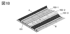


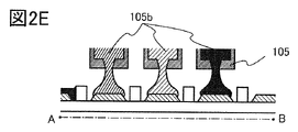


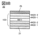

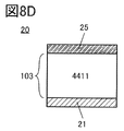


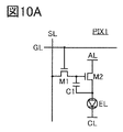


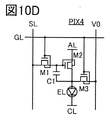

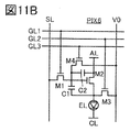


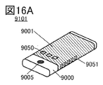

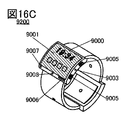


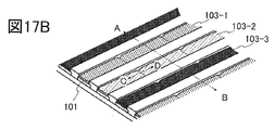


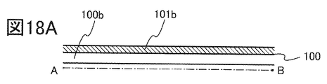
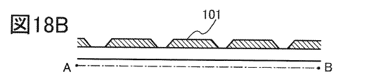


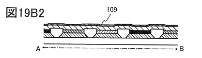
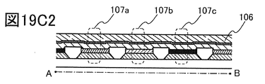


Classifications
-
- H—ELECTRICITY
- H10—SEMICONDUCTOR DEVICES; ELECTRIC SOLID-STATE DEVICES NOT OTHERWISE PROVIDED FOR
- H10K—ORGANIC ELECTRIC SOLID-STATE DEVICES
- H10K50/00—Organic light-emitting devices
- H10K50/80—Constructional details
- H10K50/805—Electrodes
- H10K50/81—Anodes
- H10K50/813—Anodes characterised by their shape
-
- H—ELECTRICITY
- H10—SEMICONDUCTOR DEVICES; ELECTRIC SOLID-STATE DEVICES NOT OTHERWISE PROVIDED FOR
- H10K—ORGANIC ELECTRIC SOLID-STATE DEVICES
- H10K59/00—Integrated devices, or assemblies of multiple devices, comprising at least one organic light-emitting element covered by group H10K50/00
- H10K59/10—OLED displays
- H10K59/12—Active-matrix OLED [AMOLED] displays
- H10K59/122—Pixel-defining structures or layers, e.g. banks
-
- G—PHYSICS
- G09—EDUCATION; CRYPTOGRAPHY; DISPLAY; ADVERTISING; SEALS
- G09F—DISPLAYING; ADVERTISING; SIGNS; LABELS OR NAME-PLATES; SEALS
- G09F9/00—Indicating arrangements for variable information in which the information is built-up on a support by selection or combination of individual elements
- G09F9/30—Indicating arrangements for variable information in which the information is built-up on a support by selection or combination of individual elements in which the desired character or characters are formed by combining individual elements
-
- H—ELECTRICITY
- H05—ELECTRIC TECHNIQUES NOT OTHERWISE PROVIDED FOR
- H05B—ELECTRIC HEATING; ELECTRIC LIGHT SOURCES NOT OTHERWISE PROVIDED FOR; CIRCUIT ARRANGEMENTS FOR ELECTRIC LIGHT SOURCES, IN GENERAL
- H05B33/00—Electroluminescent light sources
- H05B33/12—Light sources with substantially two-dimensional radiating surfaces
- H05B33/14—Light sources with substantially two-dimensional radiating surfaces characterised by the chemical or physical composition or the arrangement of the electroluminescent material, or by the simultaneous addition of the electroluminescent material in or onto the light source
-
- H—ELECTRICITY
- H05—ELECTRIC TECHNIQUES NOT OTHERWISE PROVIDED FOR
- H05B—ELECTRIC HEATING; ELECTRIC LIGHT SOURCES NOT OTHERWISE PROVIDED FOR; CIRCUIT ARRANGEMENTS FOR ELECTRIC LIGHT SOURCES, IN GENERAL
- H05B33/00—Electroluminescent light sources
- H05B33/12—Light sources with substantially two-dimensional radiating surfaces
- H05B33/22—Light sources with substantially two-dimensional radiating surfaces characterised by the chemical or physical composition or the arrangement of auxiliary dielectric or reflective layers
-
- H—ELECTRICITY
- H10—SEMICONDUCTOR DEVICES; ELECTRIC SOLID-STATE DEVICES NOT OTHERWISE PROVIDED FOR
- H10K—ORGANIC ELECTRIC SOLID-STATE DEVICES
- H10K59/00—Integrated devices, or assemblies of multiple devices, comprising at least one organic light-emitting element covered by group H10K50/00
- H10K59/30—Devices specially adapted for multicolour light emission
-
- H—ELECTRICITY
- H10—SEMICONDUCTOR DEVICES; ELECTRIC SOLID-STATE DEVICES NOT OTHERWISE PROVIDED FOR
- H10K—ORGANIC ELECTRIC SOLID-STATE DEVICES
- H10K59/00—Integrated devices, or assemblies of multiple devices, comprising at least one organic light-emitting element covered by group H10K50/00
- H10K59/80—Constructional details
- H10K59/805—Electrodes
- H10K59/8051—Anodes
- H10K59/80515—Anodes characterised by their shape
-
- H—ELECTRICITY
- H10—SEMICONDUCTOR DEVICES; ELECTRIC SOLID-STATE DEVICES NOT OTHERWISE PROVIDED FOR
- H10K—ORGANIC ELECTRIC SOLID-STATE DEVICES
- H10K59/00—Integrated devices, or assemblies of multiple devices, comprising at least one organic light-emitting element covered by group H10K50/00
- H10K59/30—Devices specially adapted for multicolour light emission
- H10K59/35—Devices specially adapted for multicolour light emission comprising red-green-blue [RGB] subpixels
Landscapes
- Engineering & Computer Science (AREA)
- Microelectronics & Electronic Packaging (AREA)
- Physics & Mathematics (AREA)
- General Physics & Mathematics (AREA)
- Theoretical Computer Science (AREA)
- Optics & Photonics (AREA)
- Electroluminescent Light Sources (AREA)
Abstract
Priority Applications (3)
| Application Number | Priority Date | Filing Date | Title |
|---|---|---|---|
| JP2022577799A JPWO2022162482A1 (fr) | 2021-01-27 | 2022-01-13 | |
| CN202280011763.9A CN116868692A (zh) | 2021-01-27 | 2022-01-13 | 发光装置、电子设备、显示装置以及照明装置 |
| US18/262,408 US20240121990A1 (en) | 2021-01-27 | 2022-01-13 | Light-emitting apparatus, electronic equipment, display apparatus, and lighting device |
Applications Claiming Priority (4)
| Application Number | Priority Date | Filing Date | Title |
|---|---|---|---|
| JP2021-011354 | 2021-01-27 | ||
| JP2021011354 | 2021-01-27 | ||
| JP2021-011206 | 2021-01-27 | ||
| JP2021011206 | 2021-01-27 |
Publications (1)
| Publication Number | Publication Date |
|---|---|
| WO2022162482A1 true WO2022162482A1 (fr) | 2022-08-04 |
Family
ID=82654212
Family Applications (1)
| Application Number | Title | Priority Date | Filing Date |
|---|---|---|---|
| PCT/IB2022/050223 WO2022162482A1 (fr) | 2021-01-27 | 2022-01-13 | Dispositif électroluminescent, équipement électronique, dispositif d'affichage et appareil d'éclairage |
Country Status (3)
| Country | Link |
|---|---|
| US (1) | US20240121990A1 (fr) |
| JP (1) | JPWO2022162482A1 (fr) |
| WO (1) | WO2022162482A1 (fr) |
Citations (5)
| Publication number | Priority date | Publication date | Assignee | Title |
|---|---|---|---|---|
| JP2005157312A (ja) * | 2003-11-22 | 2005-06-16 | Samsung Sdi Co Ltd | アクティブマトリックス有機電界発光表示装置及びその製造方法 |
| JP2010021138A (ja) * | 2008-06-09 | 2010-01-28 | Panasonic Corp | 有機エレクトロルミネッセント装置およびその製造方法 |
| JP2011210407A (ja) * | 2010-03-29 | 2011-10-20 | Sumitomo Chemical Co Ltd | 発光装置 |
| WO2020009138A1 (fr) * | 2018-07-04 | 2020-01-09 | 日産化学株式会社 | Composition de transport de charges |
| WO2020022211A1 (fr) * | 2018-07-24 | 2020-01-30 | 日産化学株式会社 | Composition de transport de charge |
-
2022
- 2022-01-13 US US18/262,408 patent/US20240121990A1/en active Pending
- 2022-01-13 WO PCT/IB2022/050223 patent/WO2022162482A1/fr active Application Filing
- 2022-01-13 JP JP2022577799A patent/JPWO2022162482A1/ja active Pending
Patent Citations (5)
| Publication number | Priority date | Publication date | Assignee | Title |
|---|---|---|---|---|
| JP2005157312A (ja) * | 2003-11-22 | 2005-06-16 | Samsung Sdi Co Ltd | アクティブマトリックス有機電界発光表示装置及びその製造方法 |
| JP2010021138A (ja) * | 2008-06-09 | 2010-01-28 | Panasonic Corp | 有機エレクトロルミネッセント装置およびその製造方法 |
| JP2011210407A (ja) * | 2010-03-29 | 2011-10-20 | Sumitomo Chemical Co Ltd | 発光装置 |
| WO2020009138A1 (fr) * | 2018-07-04 | 2020-01-09 | 日産化学株式会社 | Composition de transport de charges |
| WO2020022211A1 (fr) * | 2018-07-24 | 2020-01-30 | 日産化学株式会社 | Composition de transport de charge |
Also Published As
| Publication number | Publication date |
|---|---|
| US20240121990A1 (en) | 2024-04-11 |
| JPWO2022162482A1 (fr) | 2022-08-04 |
Similar Documents
| Publication | Publication Date | Title |
|---|---|---|
| US11963430B2 (en) | Display unit, display module, and electronic device | |
| JP7250875B2 (ja) | 発光素子 | |
| JP7292471B2 (ja) | 発光素子、表示装置、電子機器、及び照明装置 | |
| JP7174116B2 (ja) | 発光素子、発光装置、表示装置、電子機器および照明装置 | |
| KR102487578B1 (ko) | 발광 소자, 표시 장치, 전자 기기, 및 조명 장치 | |
| JP7179117B2 (ja) | 発光素子、表示装置、電子機器及び照明装置 | |
| JP7346517B2 (ja) | 発光装置 | |
| US11569466B2 (en) | Light-emitting element, light-emitting device, electronic device, and lighting device | |
| KR102543330B1 (ko) | 발광 소자, 표시 소자, 표시 장치, 전자 기기, 및 조명 장치 | |
| JP2017152695A (ja) | 発光素子、表示装置、電子機器、及び照明装置 | |
| JP2016127287A (ja) | 発光素子、発光装置、表示装置、及び電子機器 | |
| JP2016171318A (ja) | 発光素子、表示装置、電子機器、及び照明装置 | |
| JP2023024584A (ja) | 発光素子、表示装置、電子機器、及び照明装置 | |
| WO2017191526A1 (fr) | Élément électroluminescent, dispositif d'affichage, dispositif électronique et dispositif d'éclairage | |
| KR20230161406A (ko) | 헤테로 고리 화합물, 발광 소자, 발광 장치, 전자 기기, 및 조명 장치 | |
| JP2017120867A (ja) | 発光素子、表示装置、電子機器、及び照明装置 | |
| CN115347118A (zh) | 受光器件、受发光装置以及电子设备 | |
| JP7456777B2 (ja) | 発光デバイス、発光装置、電子機器および照明装置 | |
| WO2022162482A1 (fr) | Dispositif électroluminescent, équipement électronique, dispositif d'affichage et appareil d'éclairage | |
| KR20210012965A (ko) | 발광 디바이스, 발광 장치, 전자 기기, 조명 장치, 및 화합물 | |
| WO2020170074A1 (fr) | Dispositif électroluminescent, appareil électroluminescent, dispositif électronique et appareil d'éclairage | |
| CN116868692A (zh) | 发光装置、电子设备、显示装置以及照明装置 | |
| KR20240002705A (ko) | 발광 디바이스 | |
| JP2023079216A (ja) | 有機半導体素子、有機el素子、およびフォトダイオード | |
| KR20230144958A (ko) | 유기 반도체 디바이스 |
Legal Events
| Date | Code | Title | Description |
|---|---|---|---|
| 121 | Ep: the epo has been informed by wipo that ep was designated in this application |
Ref document number: 22745442 Country of ref document: EP Kind code of ref document: A1 |
|
| ENP | Entry into the national phase |
Ref document number: 2022577799 Country of ref document: JP Kind code of ref document: A |
|
| WWE | Wipo information: entry into national phase |
Ref document number: 18262408 Country of ref document: US |
|
| WWE | Wipo information: entry into national phase |
Ref document number: 202280011763.9 Country of ref document: CN |
|
| NENP | Non-entry into the national phase |
Ref country code: DE |
|
| 122 | Ep: pct application non-entry in european phase |
Ref document number: 22745442 Country of ref document: EP Kind code of ref document: A1 |