WO2022162482A1 - Light-emitting device, electronic equipment, display device, and illumination apparatus - Google Patents
Light-emitting device, electronic equipment, display device, and illumination apparatus Download PDFInfo
- Publication number
- WO2022162482A1 WO2022162482A1 PCT/IB2022/050223 IB2022050223W WO2022162482A1 WO 2022162482 A1 WO2022162482 A1 WO 2022162482A1 IB 2022050223 W IB2022050223 W IB 2022050223W WO 2022162482 A1 WO2022162482 A1 WO 2022162482A1
- Authority
- WO
- WIPO (PCT)
- Prior art keywords
- layer
- light
- emitting device
- pixel electrodes
- abbreviation
- Prior art date
Links
- 238000005286 illumination Methods 0.000 title description 2
- 238000005192 partition Methods 0.000 claims abstract description 41
- 239000000463 material Substances 0.000 claims description 231
- 238000000034 method Methods 0.000 claims description 53
- 238000005259 measurement Methods 0.000 claims description 5
- 238000002042 time-of-flight secondary ion mass spectrometry Methods 0.000 claims description 5
- 230000004888 barrier function Effects 0.000 claims description 4
- 239000010410 layer Substances 0.000 description 549
- 239000000126 substance Substances 0.000 description 99
- 238000005401 electroluminescence Methods 0.000 description 87
- 230000006870 function Effects 0.000 description 72
- 239000000758 substrate Substances 0.000 description 66
- 238000002347 injection Methods 0.000 description 61
- 239000007924 injection Substances 0.000 description 61
- -1 polyethylene terephthalate Polymers 0.000 description 60
- 150000001875 compounds Chemical class 0.000 description 44
- ODHXBMXNKOYIBV-UHFFFAOYSA-N triphenylamine Chemical compound C1=CC=CC=C1N(C=1C=CC=CC=1)C1=CC=CC=C1 ODHXBMXNKOYIBV-UHFFFAOYSA-N 0.000 description 37
- 125000001072 heteroaryl group Chemical group 0.000 description 36
- 229910052741 iridium Inorganic materials 0.000 description 34
- GKOZUEZYRPOHIO-UHFFFAOYSA-N iridium atom Chemical class [Ir] GKOZUEZYRPOHIO-UHFFFAOYSA-N 0.000 description 34
- 239000000203 mixture Substances 0.000 description 33
- 230000032258 transport Effects 0.000 description 30
- 230000005525 hole transport Effects 0.000 description 29
- 150000002894 organic compounds Chemical class 0.000 description 29
- 125000003118 aryl group Chemical group 0.000 description 28
- 239000004065 semiconductor Substances 0.000 description 28
- 210000003128 head Anatomy 0.000 description 26
- 125000001997 phenyl group Chemical class [H]C1=C([H])C([H])=C(*)C([H])=C1[H] 0.000 description 24
- 229920005989 resin Polymers 0.000 description 23
- 239000011347 resin Substances 0.000 description 23
- 239000011701 zinc Substances 0.000 description 22
- 239000000370 acceptor Substances 0.000 description 20
- 238000004519 manufacturing process Methods 0.000 description 20
- 229910052751 metal Inorganic materials 0.000 description 20
- 230000003287 optical effect Effects 0.000 description 20
- 239000007983 Tris buffer Substances 0.000 description 19
- 239000002184 metal Substances 0.000 description 19
- 230000005284 excitation Effects 0.000 description 18
- 230000002950 deficient Effects 0.000 description 17
- 229920000642 polymer Polymers 0.000 description 17
- MILUBEOXRNEUHS-UHFFFAOYSA-N iridium(3+) Chemical compound [Ir+3] MILUBEOXRNEUHS-UHFFFAOYSA-N 0.000 description 16
- 239000002131 composite material Substances 0.000 description 14
- 150000002391 heterocyclic compounds Chemical class 0.000 description 14
- 239000002253 acid Substances 0.000 description 13
- 150000001340 alkali metals Chemical class 0.000 description 13
- 230000015572 biosynthetic process Effects 0.000 description 13
- 125000000609 carbazolyl group Chemical group C1(=CC=CC=2C3=CC=CC=C3NC12)* 0.000 description 13
- 238000010586 diagram Methods 0.000 description 13
- BASFCYQUMIYNBI-UHFFFAOYSA-N platinum Chemical compound [Pt] BASFCYQUMIYNBI-UHFFFAOYSA-N 0.000 description 13
- XLOMVQKBTHCTTD-UHFFFAOYSA-N Zinc monoxide Chemical compound [Zn]=O XLOMVQKBTHCTTD-UHFFFAOYSA-N 0.000 description 12
- 239000012790 adhesive layer Substances 0.000 description 12
- 229910052783 alkali metal Inorganic materials 0.000 description 12
- 239000000872 buffer Substances 0.000 description 12
- 238000004768 lowest unoccupied molecular orbital Methods 0.000 description 12
- 230000001052 transient effect Effects 0.000 description 12
- KDLHZDBZIXYQEI-UHFFFAOYSA-N Palladium Chemical compound [Pd] KDLHZDBZIXYQEI-UHFFFAOYSA-N 0.000 description 11
- YTPLMLYBLZKORZ-UHFFFAOYSA-N Thiophene Chemical group C=1C=CSC=1 YTPLMLYBLZKORZ-UHFFFAOYSA-N 0.000 description 11
- CUJRVFIICFDLGR-UHFFFAOYSA-N acetylacetonate Chemical compound CC(=O)[CH-]C(C)=O CUJRVFIICFDLGR-UHFFFAOYSA-N 0.000 description 11
- 239000011241 protective layer Substances 0.000 description 11
- YLQBMQCUIZJEEH-UHFFFAOYSA-N Furan Chemical group C=1C=COC=1 YLQBMQCUIZJEEH-UHFFFAOYSA-N 0.000 description 10
- XUIMIQQOPSSXEZ-UHFFFAOYSA-N Silicon Chemical compound [Si] XUIMIQQOPSSXEZ-UHFFFAOYSA-N 0.000 description 10
- 229910052784 alkaline earth metal Inorganic materials 0.000 description 10
- 150000001342 alkaline earth metals Chemical class 0.000 description 10
- 150000001412 amines Chemical class 0.000 description 10
- 239000000178 monomer Substances 0.000 description 10
- 150000003335 secondary amines Chemical class 0.000 description 10
- 229910052710 silicon Inorganic materials 0.000 description 10
- 239000010703 silicon Substances 0.000 description 10
- PXHVJJICTQNCMI-UHFFFAOYSA-N Nickel Chemical group [Ni] PXHVJJICTQNCMI-UHFFFAOYSA-N 0.000 description 9
- YXFVVABEGXRONW-UHFFFAOYSA-N Toluene Chemical compound CC1=CC=CC=C1 YXFVVABEGXRONW-UHFFFAOYSA-N 0.000 description 9
- 125000004432 carbon atom Chemical group C* 0.000 description 9
- 239000003086 colorant Substances 0.000 description 9
- 125000006575 electron-withdrawing group Chemical group 0.000 description 9
- 238000012545 processing Methods 0.000 description 9
- JYEUMXHLPRZUAT-UHFFFAOYSA-N 1,2,3-triazine Chemical group C1=CN=NN=C1 JYEUMXHLPRZUAT-UHFFFAOYSA-N 0.000 description 8
- 239000000853 adhesive Substances 0.000 description 8
- 230000001070 adhesive effect Effects 0.000 description 8
- 239000000956 alloy Substances 0.000 description 8
- 125000005577 anthracene group Chemical group 0.000 description 8
- JFDZBHWFFUWGJE-UHFFFAOYSA-N benzonitrile Chemical compound N#CC1=CC=CC=C1 JFDZBHWFFUWGJE-UHFFFAOYSA-N 0.000 description 8
- 239000004305 biphenyl Substances 0.000 description 8
- 239000003990 capacitor Substances 0.000 description 8
- 238000004891 communication Methods 0.000 description 8
- 125000004093 cyano group Chemical group *C#N 0.000 description 8
- 125000001624 naphthyl group Chemical group 0.000 description 8
- 125000000168 pyrrolyl group Chemical group 0.000 description 8
- JUJWROOIHBZHMG-UHFFFAOYSA-N Pyridine Chemical group C1=CC=NC=C1 JUJWROOIHBZHMG-UHFFFAOYSA-N 0.000 description 7
- 125000005595 acetylacetonate group Chemical group 0.000 description 7
- 125000005605 benzo group Chemical group 0.000 description 7
- 230000001747 exhibiting effect Effects 0.000 description 7
- 238000002156 mixing Methods 0.000 description 7
- 229910052757 nitrogen Inorganic materials 0.000 description 7
- 238000005424 photoluminescence Methods 0.000 description 7
- UJOBWOGCFQCDNV-UHFFFAOYSA-N 9H-carbazole Chemical compound C1=CC=C2C3=CC=CC=C3NC2=C1 UJOBWOGCFQCDNV-UHFFFAOYSA-N 0.000 description 6
- UHOVQNZJYSORNB-UHFFFAOYSA-N Benzene Chemical compound C1=CC=CC=C1 UHOVQNZJYSORNB-UHFFFAOYSA-N 0.000 description 6
- XEEYBQQBJWHFJM-UHFFFAOYSA-N Iron Chemical group [Fe] XEEYBQQBJWHFJM-UHFFFAOYSA-N 0.000 description 6
- 229920001609 Poly(3,4-ethylenedioxythiophene) Polymers 0.000 description 6
- 238000010521 absorption reaction Methods 0.000 description 6
- 229910045601 alloy Inorganic materials 0.000 description 6
- 150000004982 aromatic amines Chemical class 0.000 description 6
- 150000004945 aromatic hydrocarbons Chemical class 0.000 description 6
- 230000000903 blocking effect Effects 0.000 description 6
- 150000004649 carbonic acid derivatives Chemical class 0.000 description 6
- 125000005331 diazinyl group Chemical group N1=NC(=CC=C1)* 0.000 description 6
- TXCDCPKCNAJMEE-UHFFFAOYSA-N dibenzofuran Chemical group C1=CC=C2C3=CC=CC=C3OC2=C1 TXCDCPKCNAJMEE-UHFFFAOYSA-N 0.000 description 6
- IYYZUPMFVPLQIF-ALWQSETLSA-N dibenzothiophene Chemical group C1=CC=CC=2[34S]C3=C(C=21)C=CC=C3 IYYZUPMFVPLQIF-ALWQSETLSA-N 0.000 description 6
- DKHNGUNXLDCATP-UHFFFAOYSA-N dipyrazino[2,3-f:2',3'-h]quinoxaline-2,3,6,7,10,11-hexacarbonitrile Chemical group C12=NC(C#N)=C(C#N)N=C2C2=NC(C#N)=C(C#N)N=C2C2=C1N=C(C#N)C(C#N)=N2 DKHNGUNXLDCATP-UHFFFAOYSA-N 0.000 description 6
- 150000004820 halides Chemical class 0.000 description 6
- 238000004770 highest occupied molecular orbital Methods 0.000 description 6
- 239000012535 impurity Substances 0.000 description 6
- 239000011777 magnesium Chemical group 0.000 description 6
- 239000003960 organic solvent Substances 0.000 description 6
- 125000002524 organometallic group Chemical group 0.000 description 6
- 125000003373 pyrazinyl group Chemical group 0.000 description 6
- 229910052761 rare earth metal Inorganic materials 0.000 description 6
- 150000002910 rare earth metals Chemical class 0.000 description 6
- 230000006798 recombination Effects 0.000 description 6
- 238000005215 recombination Methods 0.000 description 6
- 238000007789 sealing Methods 0.000 description 6
- 125000001424 substituent group Chemical group 0.000 description 6
- 238000012546 transfer Methods 0.000 description 6
- XLYOFNOQVPJJNP-UHFFFAOYSA-N water Substances O XLYOFNOQVPJJNP-UHFFFAOYSA-N 0.000 description 6
- 239000011787 zinc oxide Substances 0.000 description 6
- HTPBWAPZAJWXKY-UHFFFAOYSA-L zinc;quinolin-8-olate Chemical compound [Zn+2].C1=CN=C2C([O-])=CC=CC2=C1.C1=CN=C2C([O-])=CC=CC2=C1 HTPBWAPZAJWXKY-UHFFFAOYSA-L 0.000 description 6
- AZFHXIBNMPIGOD-UHFFFAOYSA-N 4-hydroxypent-3-en-2-one iridium Chemical compound [Ir].CC(O)=CC(C)=O.CC(O)=CC(C)=O.CC(O)=CC(C)=O AZFHXIBNMPIGOD-UHFFFAOYSA-N 0.000 description 5
- IJGRMHOSHXDMSA-UHFFFAOYSA-N Atomic nitrogen Chemical compound N#N IJGRMHOSHXDMSA-UHFFFAOYSA-N 0.000 description 5
- 102100022778 POC1 centriolar protein homolog A Human genes 0.000 description 5
- 101710125073 POC1 centriolar protein homolog A Proteins 0.000 description 5
- VYPSYNLAJGMNEJ-UHFFFAOYSA-N Silicium dioxide Chemical compound O=[Si]=O VYPSYNLAJGMNEJ-UHFFFAOYSA-N 0.000 description 5
- 229910052782 aluminium Inorganic materials 0.000 description 5
- 125000000319 biphenyl-4-yl group Chemical group [H]C1=C([H])C([H])=C([H])C([H])=C1C1=C([H])C([H])=C([*])C([H])=C1[H] 0.000 description 5
- 239000010949 copper Chemical group 0.000 description 5
- 238000007599 discharging Methods 0.000 description 5
- 230000000694 effects Effects 0.000 description 5
- 125000003983 fluorenyl group Chemical class C1(=CC=CC=2C3=CC=CC=C3CC12)* 0.000 description 5
- 238000010438 heat treatment Methods 0.000 description 5
- 150000002390 heteroarenes Chemical class 0.000 description 5
- 125000002883 imidazolyl group Chemical group 0.000 description 5
- 229910003437 indium oxide Inorganic materials 0.000 description 5
- PJXISJQVUVHSOJ-UHFFFAOYSA-N indium(iii) oxide Chemical compound [O-2].[O-2].[O-2].[In+3].[In+3] PJXISJQVUVHSOJ-UHFFFAOYSA-N 0.000 description 5
- 239000003446 ligand Substances 0.000 description 5
- 239000007769 metal material Substances 0.000 description 5
- QGLKJKCYBOYXKC-UHFFFAOYSA-N nonaoxidotritungsten Chemical compound O=[W]1(=O)O[W](=O)(=O)O[W](=O)(=O)O1 QGLKJKCYBOYXKC-UHFFFAOYSA-N 0.000 description 5
- IEQIEDJGQAUEQZ-UHFFFAOYSA-N phthalocyanine Chemical compound N1C(N=C2C3=CC=CC=C3C(N=C3C4=CC=CC=C4C(=N4)N3)=N2)=C(C=CC=C2)C2=C1N=C1C2=CC=CC=C2C4=N1 IEQIEDJGQAUEQZ-UHFFFAOYSA-N 0.000 description 5
- 229910052697 platinum Inorganic materials 0.000 description 5
- 239000002861 polymer material Substances 0.000 description 5
- 125000000714 pyrimidinyl group Chemical group 0.000 description 5
- 230000002441 reversible effect Effects 0.000 description 5
- 125000000020 sulfo group Chemical group O=S(=O)([*])O[H] 0.000 description 5
- 150000003512 tertiary amines Chemical class 0.000 description 5
- 229910001930 tungsten oxide Inorganic materials 0.000 description 5
- 229920000178 Acrylic resin Polymers 0.000 description 4
- 239000004925 Acrylic resin Substances 0.000 description 4
- RYGMFSIKBFXOCR-UHFFFAOYSA-N Copper Chemical group [Cu] RYGMFSIKBFXOCR-UHFFFAOYSA-N 0.000 description 4
- GYHNNYVSQQEPJS-UHFFFAOYSA-N Gallium Chemical group [Ga] GYHNNYVSQQEPJS-UHFFFAOYSA-N 0.000 description 4
- FYYHWMGAXLPEAU-UHFFFAOYSA-N Magnesium Chemical group [Mg] FYYHWMGAXLPEAU-UHFFFAOYSA-N 0.000 description 4
- ZOKXTWBITQBERF-UHFFFAOYSA-N Molybdenum Chemical group [Mo] ZOKXTWBITQBERF-UHFFFAOYSA-N 0.000 description 4
- 102100022769 POC1 centriolar protein homolog B Human genes 0.000 description 4
- 101710125069 POC1 centriolar protein homolog B Proteins 0.000 description 4
- ATJFFYVFTNAWJD-UHFFFAOYSA-N Tin Chemical group [Sn] ATJFFYVFTNAWJD-UHFFFAOYSA-N 0.000 description 4
- DGEZNRSVGBDHLK-UHFFFAOYSA-N [1,10]phenanthroline Chemical compound C1=CN=C2C3=NC=CC=C3C=CC2=C1 DGEZNRSVGBDHLK-UHFFFAOYSA-N 0.000 description 4
- DZBUGLKDJFMEHC-UHFFFAOYSA-N acridine Chemical compound C1=CC=CC2=CC3=CC=CC=C3N=C21 DZBUGLKDJFMEHC-UHFFFAOYSA-N 0.000 description 4
- 125000000217 alkyl group Chemical group 0.000 description 4
- XAGFODPZIPBFFR-UHFFFAOYSA-N aluminium Chemical group [Al] XAGFODPZIPBFFR-UHFFFAOYSA-N 0.000 description 4
- 229910052796 boron Inorganic materials 0.000 description 4
- XJHCXCQVJFPJIK-UHFFFAOYSA-M caesium fluoride Chemical compound [F-].[Cs+] XJHCXCQVJFPJIK-UHFFFAOYSA-M 0.000 description 4
- 239000000969 carrier Substances 0.000 description 4
- 239000011651 chromium Substances 0.000 description 4
- 229910052802 copper Inorganic materials 0.000 description 4
- 230000003111 delayed effect Effects 0.000 description 4
- ZUOUZKKEUPVFJK-UHFFFAOYSA-N diphenyl Chemical compound C1=CC=CC=C1C1=CC=CC=C1 ZUOUZKKEUPVFJK-UHFFFAOYSA-N 0.000 description 4
- 238000001035 drying Methods 0.000 description 4
- 238000000295 emission spectrum Methods 0.000 description 4
- 239000003822 epoxy resin Substances 0.000 description 4
- 150000002222 fluorine compounds Chemical class 0.000 description 4
- 229910052733 gallium Inorganic materials 0.000 description 4
- 239000011521 glass Substances 0.000 description 4
- 125000005843 halogen group Chemical group 0.000 description 4
- AMWRITDGCCNYAT-UHFFFAOYSA-L hydroxy(oxo)manganese;manganese Chemical compound [Mn].O[Mn]=O.O[Mn]=O AMWRITDGCCNYAT-UHFFFAOYSA-L 0.000 description 4
- 238000003384 imaging method Methods 0.000 description 4
- 229910052738 indium Inorganic materials 0.000 description 4
- APFVFJFRJDLVQX-UHFFFAOYSA-N indium atom Chemical compound [In] APFVFJFRJDLVQX-UHFFFAOYSA-N 0.000 description 4
- 229910052749 magnesium Chemical group 0.000 description 4
- 229910044991 metal oxide Inorganic materials 0.000 description 4
- 150000004706 metal oxides Chemical class 0.000 description 4
- 229910052750 molybdenum Inorganic materials 0.000 description 4
- 239000011733 molybdenum Chemical group 0.000 description 4
- 229910052759 nickel Inorganic materials 0.000 description 4
- 229910052763 palladium Inorganic materials 0.000 description 4
- YNPNZTXNASCQKK-UHFFFAOYSA-N phenanthrene Chemical group C1=CC=C2C3=CC=CC=C3C=CC2=C1 YNPNZTXNASCQKK-UHFFFAOYSA-N 0.000 description 4
- 229920000647 polyepoxide Polymers 0.000 description 4
- 230000008569 process Effects 0.000 description 4
- 230000001681 protective effect Effects 0.000 description 4
- 230000009467 reduction Effects 0.000 description 4
- 229910052814 silicon oxide Inorganic materials 0.000 description 4
- 239000002356 single layer Substances 0.000 description 4
- PUZPDOWCWNUUKD-UHFFFAOYSA-M sodium fluoride Chemical compound [F-].[Na+] PUZPDOWCWNUUKD-UHFFFAOYSA-M 0.000 description 4
- 238000003860 storage Methods 0.000 description 4
- 150000003457 sulfones Chemical class 0.000 description 4
- 150000003577 thiophenes Chemical class 0.000 description 4
- 229910052718 tin Inorganic materials 0.000 description 4
- WFKWXMTUELFFGS-UHFFFAOYSA-N tungsten Chemical group [W] WFKWXMTUELFFGS-UHFFFAOYSA-N 0.000 description 4
- 229910052721 tungsten Inorganic materials 0.000 description 4
- 239000010937 tungsten Chemical group 0.000 description 4
- 125000000391 vinyl group Chemical group [H]C([*])=C([H])[H] 0.000 description 4
- 229910052727 yttrium Inorganic materials 0.000 description 4
- SPDPTFAJSFKAMT-UHFFFAOYSA-N 1-n-[4-[4-(n-[4-(3-methyl-n-(3-methylphenyl)anilino)phenyl]anilino)phenyl]phenyl]-4-n,4-n-bis(3-methylphenyl)-1-n-phenylbenzene-1,4-diamine Chemical compound CC1=CC=CC(N(C=2C=CC(=CC=2)N(C=2C=CC=CC=2)C=2C=CC(=CC=2)C=2C=CC(=CC=2)N(C=2C=CC=CC=2)C=2C=CC(=CC=2)N(C=2C=C(C)C=CC=2)C=2C=C(C)C=CC=2)C=2C=C(C)C=CC=2)=C1 SPDPTFAJSFKAMT-UHFFFAOYSA-N 0.000 description 3
- IXHWGNYCZPISET-UHFFFAOYSA-N 2-[4-(dicyanomethylidene)-2,3,5,6-tetrafluorocyclohexa-2,5-dien-1-ylidene]propanedinitrile Chemical compound FC1=C(F)C(=C(C#N)C#N)C(F)=C(F)C1=C(C#N)C#N IXHWGNYCZPISET-UHFFFAOYSA-N 0.000 description 3
- FCNCGHJSNVOIKE-UHFFFAOYSA-N 9,10-diphenylanthracene Chemical group C1=CC=CC=C1C(C1=CC=CC=C11)=C(C=CC=C2)C2=C1C1=CC=CC=C1 FCNCGHJSNVOIKE-UHFFFAOYSA-N 0.000 description 3
- WEVYAHXRMPXWCK-UHFFFAOYSA-N Acetonitrile Chemical compound CC#N WEVYAHXRMPXWCK-UHFFFAOYSA-N 0.000 description 3
- ZOXJGFHDIHLPTG-UHFFFAOYSA-N Boron Chemical group [B] ZOXJGFHDIHLPTG-UHFFFAOYSA-N 0.000 description 3
- VYZAMTAEIAYCRO-UHFFFAOYSA-N Chromium Chemical compound [Cr] VYZAMTAEIAYCRO-UHFFFAOYSA-N 0.000 description 3
- YMWUJEATGCHHMB-UHFFFAOYSA-N Dichloromethane Chemical compound ClCCl YMWUJEATGCHHMB-UHFFFAOYSA-N 0.000 description 3
- LFQSCWFLJHTTHZ-UHFFFAOYSA-N Ethanol Chemical compound CCO LFQSCWFLJHTTHZ-UHFFFAOYSA-N 0.000 description 3
- XEKOWRVHYACXOJ-UHFFFAOYSA-N Ethyl acetate Chemical compound CCOC(C)=O XEKOWRVHYACXOJ-UHFFFAOYSA-N 0.000 description 3
- 229910052693 Europium Inorganic materials 0.000 description 3
- OKKJLVBELUTLKV-UHFFFAOYSA-N Methanol Chemical compound OC OKKJLVBELUTLKV-UHFFFAOYSA-N 0.000 description 3
- ZMXDDKWLCZADIW-UHFFFAOYSA-N N,N-Dimethylformamide Chemical compound CN(C)C=O ZMXDDKWLCZADIW-UHFFFAOYSA-N 0.000 description 3
- CTQNGGLPUBDAKN-UHFFFAOYSA-N O-Xylene Chemical compound CC1=CC=CC=C1C CTQNGGLPUBDAKN-UHFFFAOYSA-N 0.000 description 3
- 229920000265 Polyparaphenylene Polymers 0.000 description 3
- 229910052581 Si3N4 Inorganic materials 0.000 description 3
- 229910008449 SnF 2 Inorganic materials 0.000 description 3
- RTAQQCXQSZGOHL-UHFFFAOYSA-N Titanium Chemical group [Ti] RTAQQCXQSZGOHL-UHFFFAOYSA-N 0.000 description 3
- AZWHFTKIBIQKCA-UHFFFAOYSA-N [Sn+2]=O.[O-2].[In+3] Chemical compound [Sn+2]=O.[O-2].[In+3] AZWHFTKIBIQKCA-UHFFFAOYSA-N 0.000 description 3
- 230000001133 acceleration Effects 0.000 description 3
- 238000004458 analytical method Methods 0.000 description 3
- 229910052804 chromium Inorganic materials 0.000 description 3
- 230000000295 complement effect Effects 0.000 description 3
- 239000004020 conductor Substances 0.000 description 3
- 229920000547 conjugated polymer Polymers 0.000 description 3
- 150000004696 coordination complex Chemical class 0.000 description 3
- 239000000412 dendrimer Substances 0.000 description 3
- 229920000736 dendritic polymer Polymers 0.000 description 3
- 238000009792 diffusion process Methods 0.000 description 3
- 230000005684 electric field Effects 0.000 description 3
- OGPBJKLSAFTDLK-UHFFFAOYSA-N europium atom Chemical compound [Eu] OGPBJKLSAFTDLK-UHFFFAOYSA-N 0.000 description 3
- 125000001153 fluoro group Chemical group F* 0.000 description 3
- 239000010931 gold Substances 0.000 description 3
- LNEPOXFFQSENCJ-UHFFFAOYSA-N haloperidol Chemical compound C1CC(O)(C=2C=CC(Cl)=CC=2)CCN1CCCC(=O)C1=CC=C(F)C=C1 LNEPOXFFQSENCJ-UHFFFAOYSA-N 0.000 description 3
- 150000002500 ions Chemical class 0.000 description 3
- 239000007788 liquid Substances 0.000 description 3
- 239000003550 marker Substances 0.000 description 3
- AUHZEENZYGFFBQ-UHFFFAOYSA-N mesitylene Substances CC1=CC(C)=CC(C)=C1 AUHZEENZYGFFBQ-UHFFFAOYSA-N 0.000 description 3
- 125000001827 mesitylenyl group Chemical group [H]C1=C(C(*)=C(C([H])=C1C([H])([H])[H])C([H])([H])[H])C([H])([H])[H] 0.000 description 3
- 150000002739 metals Chemical class 0.000 description 3
- 230000004048 modification Effects 0.000 description 3
- 238000012986 modification Methods 0.000 description 3
- VLKZOEOYAKHREP-UHFFFAOYSA-N n-Hexane Chemical compound CCCCCC VLKZOEOYAKHREP-UHFFFAOYSA-N 0.000 description 3
- 150000004767 nitrides Chemical class 0.000 description 3
- 125000001792 phenanthrenyl group Chemical group C1(=CC=CC=2C3=CC=CC=C3C=CC12)* 0.000 description 3
- 125000001484 phenothiazinyl group Chemical group C1(=CC=CC=2SC3=CC=CC=C3NC12)* 0.000 description 3
- 125000001644 phenoxazinyl group Chemical group C1(=CC=CC=2OC3=CC=CC=C3NC12)* 0.000 description 3
- 229920003227 poly(N-vinyl carbazole) Polymers 0.000 description 3
- 229910021420 polycrystalline silicon Inorganic materials 0.000 description 3
- 229920001721 polyimide Polymers 0.000 description 3
- 239000009719 polyimide resin Substances 0.000 description 3
- 239000004800 polyvinyl chloride Substances 0.000 description 3
- 229920000915 polyvinyl chloride Polymers 0.000 description 3
- 150000004032 porphyrins Chemical class 0.000 description 3
- 125000006239 protecting group Chemical group 0.000 description 3
- PBMFSQRYOILNGV-UHFFFAOYSA-N pyridazine Chemical group C1=CC=NN=C1 PBMFSQRYOILNGV-UHFFFAOYSA-N 0.000 description 3
- 230000004044 response Effects 0.000 description 3
- HQVNEWCFYHHQES-UHFFFAOYSA-N silicon nitride Chemical compound N12[Si]34N5[Si]62N3[Si]51N64 HQVNEWCFYHHQES-UHFFFAOYSA-N 0.000 description 3
- 229910052709 silver Inorganic materials 0.000 description 3
- 238000004544 sputter deposition Methods 0.000 description 3
- ANOBYBYXJXCGBS-UHFFFAOYSA-L stannous fluoride Chemical compound F[Sn]F ANOBYBYXJXCGBS-UHFFFAOYSA-L 0.000 description 3
- JBQYATWDVHIOAR-UHFFFAOYSA-N tellanylidenegermanium Chemical compound [Te]=[Ge] JBQYATWDVHIOAR-UHFFFAOYSA-N 0.000 description 3
- 229910052719 titanium Inorganic materials 0.000 description 3
- 239000010936 titanium Chemical group 0.000 description 3
- 150000003852 triazoles Chemical group 0.000 description 3
- 239000008096 xylene Substances 0.000 description 3
- VWQVUPCCIRVNHF-UHFFFAOYSA-N yttrium atom Chemical group [Y] VWQVUPCCIRVNHF-UHFFFAOYSA-N 0.000 description 3
- XOYZGLGJSAZOAG-UHFFFAOYSA-N 1-n,1-n,4-n-triphenyl-4-n-[4-[4-(n-[4-(n-phenylanilino)phenyl]anilino)phenyl]phenyl]benzene-1,4-diamine Chemical group C1=CC=CC=C1N(C=1C=CC(=CC=1)N(C=1C=CC=CC=1)C=1C=CC(=CC=1)C=1C=CC(=CC=1)N(C=1C=CC=CC=1)C=1C=CC(=CC=1)N(C=1C=CC=CC=1)C=1C=CC=CC=1)C1=CC=CC=C1 XOYZGLGJSAZOAG-UHFFFAOYSA-N 0.000 description 2
- ZABORCXHTNWZRV-UHFFFAOYSA-N 10-[4-(4,6-diphenyl-1,3,5-triazin-2-yl)phenyl]phenoxazine Chemical compound O1C2=CC=CC=C2N(C2=CC=C(C=C2)C2=NC(=NC(=N2)C2=CC=CC=C2)C2=CC=CC=C2)C2=C1C=CC=C2 ZABORCXHTNWZRV-UHFFFAOYSA-N 0.000 description 2
- ASXSTQHYXCIZRV-UHFFFAOYSA-N 10-phenylspiro[acridine-9,10'-anthracene]-9'-one Chemical compound C12=CC=CC=C2C(=O)C2=CC=CC=C2C1(C1=CC=CC=C11)C2=CC=CC=C2N1C1=CC=CC=C1 ASXSTQHYXCIZRV-UHFFFAOYSA-N 0.000 description 2
- MYKQKWIPLZEVOW-UHFFFAOYSA-N 11h-benzo[a]carbazole Chemical group C1=CC2=CC=CC=C2C2=C1C1=CC=CC=C1N2 MYKQKWIPLZEVOW-UHFFFAOYSA-N 0.000 description 2
- QWENRTYMTSOGBR-UHFFFAOYSA-N 1H-1,2,3-Triazole Chemical group C=1C=NNN=1 QWENRTYMTSOGBR-UHFFFAOYSA-N 0.000 description 2
- XESMNQMWRSEIET-UHFFFAOYSA-N 2,9-dinaphthalen-2-yl-4,7-diphenyl-1,10-phenanthroline Chemical compound C1=CC=CC=C1C1=CC(C=2C=C3C=CC=CC3=CC=2)=NC2=C1C=CC1=C(C=3C=CC=CC=3)C=C(C=3C=C4C=CC=CC4=CC=3)N=C21 XESMNQMWRSEIET-UHFFFAOYSA-N 0.000 description 2
- FQJQNLKWTRGIEB-UHFFFAOYSA-N 2-(4-tert-butylphenyl)-5-[3-[5-(4-tert-butylphenyl)-1,3,4-oxadiazol-2-yl]phenyl]-1,3,4-oxadiazole Chemical compound C1=CC(C(C)(C)C)=CC=C1C1=NN=C(C=2C=C(C=CC=2)C=2OC(=NN=2)C=2C=CC(=CC=2)C(C)(C)C)O1 FQJQNLKWTRGIEB-UHFFFAOYSA-N 0.000 description 2
- GEQBRULPNIVQPP-UHFFFAOYSA-N 2-[3,5-bis(1-phenylbenzimidazol-2-yl)phenyl]-1-phenylbenzimidazole Chemical compound C1=CC=CC=C1N1C2=CC=CC=C2N=C1C1=CC(C=2N(C3=CC=CC=C3N=2)C=2C=CC=CC=2)=CC(C=2N(C3=CC=CC=C3N=2)C=2C=CC=CC=2)=C1 GEQBRULPNIVQPP-UHFFFAOYSA-N 0.000 description 2
- ZVFQEOPUXVPSLB-UHFFFAOYSA-N 3-(4-tert-butylphenyl)-4-phenyl-5-(4-phenylphenyl)-1,2,4-triazole Chemical compound C1=CC(C(C)(C)C)=CC=C1C(N1C=2C=CC=CC=2)=NN=C1C1=CC=C(C=2C=CC=CC=2)C=C1 ZVFQEOPUXVPSLB-UHFFFAOYSA-N 0.000 description 2
- FTZXDZQJFKXEGW-UHFFFAOYSA-N 3-(9,9-dimethylacridin-10-yl)xanthen-9-one Chemical compound C12=CC=CC=C2C(C)(C)C2=CC=CC=C2N1C1=CC=C2C(=O)C3=CC=CC=C3OC2=C1 FTZXDZQJFKXEGW-UHFFFAOYSA-N 0.000 description 2
- GKTLHQFSIDFAJH-UHFFFAOYSA-N 3-(9h-carbazol-3-yl)-9-phenylcarbazole Chemical group C1=CC=CC=C1N1C2=CC=C(C=3C=C4C5=CC=CC=C5NC4=CC=3)C=C2C2=CC=CC=C21 GKTLHQFSIDFAJH-UHFFFAOYSA-N 0.000 description 2
- CINYXYWQPZSTOT-UHFFFAOYSA-N 3-[3-[3,5-bis(3-pyridin-3-ylphenyl)phenyl]phenyl]pyridine Chemical compound C1=CN=CC(C=2C=C(C=CC=2)C=2C=C(C=C(C=2)C=2C=C(C=CC=2)C=2C=NC=CC=2)C=2C=C(C=CC=2)C=2C=NC=CC=2)=C1 CINYXYWQPZSTOT-UHFFFAOYSA-N 0.000 description 2
- DHDHJYNTEFLIHY-UHFFFAOYSA-N 4,7-diphenyl-1,10-phenanthroline Chemical compound C1=CC=CC=C1C1=CC=NC2=C1C=CC1=C(C=3C=CC=CC=3)C=CN=C21 DHDHJYNTEFLIHY-UHFFFAOYSA-N 0.000 description 2
- BGEVROQFKHXUQA-UHFFFAOYSA-N 71012-25-4 Chemical group C12=CC=CC=C2C2=CC=CC=C2C2=C1C1=CC=CC=C1N2 BGEVROQFKHXUQA-UHFFFAOYSA-N 0.000 description 2
- RZVHIXYEVGDQDX-UHFFFAOYSA-N 9,10-anthraquinone Chemical group C1=CC=C2C(=O)C3=CC=CC=C3C(=O)C2=C1 RZVHIXYEVGDQDX-UHFFFAOYSA-N 0.000 description 2
- GJWBRYKOJMOBHH-UHFFFAOYSA-N 9,9-dimethyl-n-[4-(9-phenylcarbazol-3-yl)phenyl]-n-(4-phenylphenyl)fluoren-2-amine Chemical compound C1=C2C(C)(C)C3=CC=CC=C3C2=CC=C1N(C=1C=CC(=CC=1)C=1C=C2C3=CC=CC=C3N(C=3C=CC=CC=3)C2=CC=1)C(C=C1)=CC=C1C1=CC=CC=C1 GJWBRYKOJMOBHH-UHFFFAOYSA-N 0.000 description 2
- VDHOGVHFPFGPIP-UHFFFAOYSA-N 9-[3-[5-(3-carbazol-9-ylphenyl)pyridin-3-yl]phenyl]carbazole Chemical compound C12=CC=CC=C2C2=CC=CC=C2N1C1=CC(C=2C=NC=C(C=2)C=2C=CC=C(C=2)N2C3=CC=CC=C3C3=CC=CC=C32)=CC=C1 VDHOGVHFPFGPIP-UHFFFAOYSA-N 0.000 description 2
- VFUDMQLBKNMONU-UHFFFAOYSA-N 9-[4-(4-carbazol-9-ylphenyl)phenyl]carbazole Chemical group C12=CC=CC=C2C2=CC=CC=C2N1C1=CC=C(C=2C=CC(=CC=2)N2C3=CC=CC=C3C3=CC=CC=C32)C=C1 VFUDMQLBKNMONU-UHFFFAOYSA-N 0.000 description 2
- PQJUJGAVDBINPI-UHFFFAOYSA-N 9H-thioxanthene Chemical compound C1=CC=C2CC3=CC=CC=C3SC2=C1 PQJUJGAVDBINPI-UHFFFAOYSA-N 0.000 description 2
- 101100082458 Arabidopsis thaliana PBL34 gene Proteins 0.000 description 2
- 101100034357 Arabidopsis thaliana RIPK gene Proteins 0.000 description 2
- XKRFYHLGVUSROY-UHFFFAOYSA-N Argon Chemical compound [Ar] XKRFYHLGVUSROY-UHFFFAOYSA-N 0.000 description 2
- ROFVEXUMMXZLPA-UHFFFAOYSA-N Bipyridyl Chemical class N1=CC=CC=C1C1=CC=CC=N1 ROFVEXUMMXZLPA-UHFFFAOYSA-N 0.000 description 2
- LSNNMFCWUKXFEE-UHFFFAOYSA-M Bisulfite Chemical compound OS([O-])=O LSNNMFCWUKXFEE-UHFFFAOYSA-M 0.000 description 2
- WGXBVAMMNYFGSZ-UHFFFAOYSA-N C1=CC=CC=C1N(C1=CC=C(C2=C3SC4=C(C3=CC=C2)C=CC=C4)C=C1)C1=CC=C(C=C1)C1=CC=CC=C1 Chemical compound C1=CC=CC=C1N(C1=CC=C(C2=C3SC4=C(C3=CC=C2)C=CC=C4)C=C1)C1=CC=C(C=C1)C1=CC=CC=C1 WGXBVAMMNYFGSZ-UHFFFAOYSA-N 0.000 description 2
- XMWRBQBLMFGWIX-UHFFFAOYSA-N C60 fullerene Chemical compound C12=C3C(C4=C56)=C7C8=C5C5=C9C%10=C6C6=C4C1=C1C4=C6C6=C%10C%10=C9C9=C%11C5=C8C5=C8C7=C3C3=C7C2=C1C1=C2C4=C6C4=C%10C6=C9C9=C%11C5=C5C8=C3C3=C7C1=C1C2=C4C6=C2C9=C5C3=C12 XMWRBQBLMFGWIX-UHFFFAOYSA-N 0.000 description 2
- OKTJSMMVPCPJKN-UHFFFAOYSA-N Carbon Chemical compound [C] OKTJSMMVPCPJKN-UHFFFAOYSA-N 0.000 description 2
- 229920002284 Cellulose triacetate Polymers 0.000 description 2
- HEDRZPFGACZZDS-UHFFFAOYSA-N Chloroform Chemical compound ClC(Cl)Cl HEDRZPFGACZZDS-UHFFFAOYSA-N 0.000 description 2
- 229920000089 Cyclic olefin copolymer Polymers 0.000 description 2
- IAZDPXIOMUYVGZ-UHFFFAOYSA-N Dimethylsulphoxide Chemical compound CS(C)=O IAZDPXIOMUYVGZ-UHFFFAOYSA-N 0.000 description 2
- KFZMGEQAYNKOFK-UHFFFAOYSA-N Isopropanol Chemical compound CC(C)O KFZMGEQAYNKOFK-UHFFFAOYSA-N 0.000 description 2
- IMUWJDCTOIKWNR-UHFFFAOYSA-N N-(4-naphthalen-1-ylphenyl)-N-[3-(6-phenyldibenzofuran-4-yl)phenyl]naphthalen-1-amine Chemical compound O1C2=C(C=CC=C2C2=CC=CC=C2)C2=C1C(=CC=C2)C1=CC=CC(=C1)N(C1=CC=C(C=C1)C1=CC=CC2=C1C=CC=C2)C1=C2C=CC=CC2=CC=C1 IMUWJDCTOIKWNR-UHFFFAOYSA-N 0.000 description 2
- LRHPLDYGYMQRHN-UHFFFAOYSA-N N-Butanol Chemical compound CCCCO LRHPLDYGYMQRHN-UHFFFAOYSA-N 0.000 description 2
- 239000004677 Nylon Substances 0.000 description 2
- 239000004793 Polystyrene Substances 0.000 description 2
- KYQCOXFCLRTKLS-UHFFFAOYSA-N Pyrazine Chemical compound C1=CN=CC=N1 KYQCOXFCLRTKLS-UHFFFAOYSA-N 0.000 description 2
- CZPWVGJYEJSRLH-UHFFFAOYSA-N Pyrimidine Chemical compound C1=CN=CN=C1 CZPWVGJYEJSRLH-UHFFFAOYSA-N 0.000 description 2
- SMWDFEZZVXVKRB-UHFFFAOYSA-N Quinoline Chemical compound N1=CC=CC2=CC=CC=C21 SMWDFEZZVXVKRB-UHFFFAOYSA-N 0.000 description 2
- BQCADISMDOOEFD-UHFFFAOYSA-N Silver Chemical compound [Ag] BQCADISMDOOEFD-UHFFFAOYSA-N 0.000 description 2
- DKGAVHZHDRPRBM-UHFFFAOYSA-N Tert-Butanol Chemical compound CC(C)(C)O DKGAVHZHDRPRBM-UHFFFAOYSA-N 0.000 description 2
- WYURNTSHIVDZCO-UHFFFAOYSA-N Tetrahydrofuran Chemical compound C1CCOC1 WYURNTSHIVDZCO-UHFFFAOYSA-N 0.000 description 2
- NRTOMJZYCJJWKI-UHFFFAOYSA-N Titanium nitride Chemical compound [Ti]#N NRTOMJZYCJJWKI-UHFFFAOYSA-N 0.000 description 2
- 206010047571 Visual impairment Diseases 0.000 description 2
- QCWXUUIWCKQGHC-UHFFFAOYSA-N Zirconium Chemical group [Zr] QCWXUUIWCKQGHC-UHFFFAOYSA-N 0.000 description 2
- NNLVGZFZQQXQNW-ADJNRHBOSA-N [(2r,3r,4s,5r,6s)-4,5-diacetyloxy-3-[(2s,3r,4s,5r,6r)-3,4,5-triacetyloxy-6-(acetyloxymethyl)oxan-2-yl]oxy-6-[(2r,3r,4s,5r,6s)-4,5,6-triacetyloxy-2-(acetyloxymethyl)oxan-3-yl]oxyoxan-2-yl]methyl acetate Chemical compound O([C@@H]1O[C@@H]([C@H]([C@H](OC(C)=O)[C@H]1OC(C)=O)O[C@H]1[C@@H]([C@@H](OC(C)=O)[C@H](OC(C)=O)[C@@H](COC(C)=O)O1)OC(C)=O)COC(=O)C)[C@@H]1[C@@H](COC(C)=O)O[C@@H](OC(C)=O)[C@H](OC(C)=O)[C@H]1OC(C)=O NNLVGZFZQQXQNW-ADJNRHBOSA-N 0.000 description 2
- HYWNGEYOXQESBM-UHFFFAOYSA-N [1]benzofuro[2,3-b]pyrazine Chemical group C1=CN=C2C3=CC=CC=C3OC2=N1 HYWNGEYOXQESBM-UHFFFAOYSA-N 0.000 description 2
- ITOKSWHFPQBNSE-UHFFFAOYSA-N [1]benzofuro[3,2-d]pyrimidine Chemical group N1=CN=C2C3=CC=CC=C3OC2=C1 ITOKSWHFPQBNSE-UHFFFAOYSA-N 0.000 description 2
- BJHVGSLMZTVDRA-UHFFFAOYSA-N [1]benzothiolo[2,3-b]pyrazine Chemical group C1=CN=C2C3=CC=CC=C3SC2=N1 BJHVGSLMZTVDRA-UHFFFAOYSA-N 0.000 description 2
- OICJTSLHQGDCTQ-UHFFFAOYSA-N [1]benzothiolo[3,2-d]pyrimidine Chemical group N1=CN=C2C3=CC=CC=C3SC2=C1 OICJTSLHQGDCTQ-UHFFFAOYSA-N 0.000 description 2
- XHCLAFWTIXFWPH-UHFFFAOYSA-N [O-2].[O-2].[O-2].[O-2].[O-2].[V+5].[V+5] Chemical compound [O-2].[O-2].[O-2].[O-2].[O-2].[V+5].[V+5] XHCLAFWTIXFWPH-UHFFFAOYSA-N 0.000 description 2
- 150000007513 acids Chemical class 0.000 description 2
- 125000000641 acridinyl group Chemical group C1(=CC=CC2=NC3=CC=CC=C3C=C12)* 0.000 description 2
- 150000001339 alkali metal compounds Chemical class 0.000 description 2
- 150000001341 alkaline earth metal compounds Chemical class 0.000 description 2
- 229910021417 amorphous silicon Inorganic materials 0.000 description 2
- 125000005428 anthryl group Chemical group [H]C1=C([H])C([H])=C2C([H])=C3C(*)=C([H])C([H])=C([H])C3=C([H])C2=C1[H] 0.000 description 2
- 239000012298 atmosphere Substances 0.000 description 2
- 229910052788 barium Inorganic materials 0.000 description 2
- DSAJWYNOEDNPEQ-UHFFFAOYSA-N barium atom Chemical compound [Ba] DSAJWYNOEDNPEQ-UHFFFAOYSA-N 0.000 description 2
- 230000008901 benefit Effects 0.000 description 2
- WZJYKHNJTSNBHV-UHFFFAOYSA-N benzo[h]quinoline Chemical class C1=CN=C2C3=CC=CC=C3C=CC2=C1 WZJYKHNJTSNBHV-UHFFFAOYSA-N 0.000 description 2
- RWCCWEUUXYIKHB-UHFFFAOYSA-N benzophenone Chemical compound C=1C=CC=CC=1C(=O)C1=CC=CC=C1 RWCCWEUUXYIKHB-UHFFFAOYSA-N 0.000 description 2
- 239000012965 benzophenone Substances 0.000 description 2
- 235000010290 biphenyl Nutrition 0.000 description 2
- DMVOXQPQNTYEKQ-UHFFFAOYSA-N biphenyl-4-amine Chemical compound C1=CC(N)=CC=C1C1=CC=CC=C1 DMVOXQPQNTYEKQ-UHFFFAOYSA-N 0.000 description 2
- 210000005252 bulbus oculi Anatomy 0.000 description 2
- DQXBYHZEEUGOBF-UHFFFAOYSA-N but-3-enoic acid;ethene Chemical compound C=C.OC(=O)CC=C DQXBYHZEEUGOBF-UHFFFAOYSA-N 0.000 description 2
- 229910052793 cadmium Inorganic materials 0.000 description 2
- BDOSMKKIYDKNTQ-UHFFFAOYSA-N cadmium atom Chemical compound [Cd] BDOSMKKIYDKNTQ-UHFFFAOYSA-N 0.000 description 2
- FJDQFPXHSGXQBY-UHFFFAOYSA-L caesium carbonate Chemical compound [Cs+].[Cs+].[O-]C([O-])=O FJDQFPXHSGXQBY-UHFFFAOYSA-L 0.000 description 2
- 229910000024 caesium carbonate Inorganic materials 0.000 description 2
- 125000002915 carbonyl group Chemical group [*:2]C([*:1])=O 0.000 description 2
- 238000006243 chemical reaction Methods 0.000 description 2
- 239000008199 coating composition Substances 0.000 description 2
- 229910017052 cobalt Inorganic materials 0.000 description 2
- 239000010941 cobalt Substances 0.000 description 2
- GUTLYIVDDKVIGB-UHFFFAOYSA-N cobalt atom Chemical compound [Co] GUTLYIVDDKVIGB-UHFFFAOYSA-N 0.000 description 2
- 229920001577 copolymer Polymers 0.000 description 2
- KZPXREABEBSAQM-UHFFFAOYSA-N cyclopenta-1,3-diene;nickel(2+) Chemical compound [Ni+2].C=1C=C[CH-]C=1.C=1C=C[CH-]C=1 KZPXREABEBSAQM-UHFFFAOYSA-N 0.000 description 2
- 238000001514 detection method Methods 0.000 description 2
- 230000006866 deterioration Effects 0.000 description 2
- IYYZUPMFVPLQIF-UHFFFAOYSA-N dibenzothiophene Chemical compound C1=CC=C2C3=CC=CC=C3SC2=C1 IYYZUPMFVPLQIF-UHFFFAOYSA-N 0.000 description 2
- XBDQKXXYIPTUBI-UHFFFAOYSA-N dimethylselenoniopropionate Natural products CCC(O)=O XBDQKXXYIPTUBI-UHFFFAOYSA-N 0.000 description 2
- 238000006073 displacement reaction Methods 0.000 description 2
- YQGOJNYOYNNSMM-UHFFFAOYSA-N eosin Chemical class [Na+].OC(=O)C1=CC=CC=C1C1=C2C=C(Br)C(=O)C(Br)=C2OC2=C(Br)C(O)=C(Br)C=C21 YQGOJNYOYNNSMM-UHFFFAOYSA-N 0.000 description 2
- RTZKZFJDLAIYFH-UHFFFAOYSA-N ether Substances CCOCC RTZKZFJDLAIYFH-UHFFFAOYSA-N 0.000 description 2
- 239000005038 ethylene vinyl acetate Substances 0.000 description 2
- 230000005281 excited state Effects 0.000 description 2
- 239000000284 extract Substances 0.000 description 2
- NIHNNTQXNPWCJQ-UHFFFAOYSA-N fluorene Chemical compound C1=CC=C2CC3=CC=CC=C3C2=C1 NIHNNTQXNPWCJQ-UHFFFAOYSA-N 0.000 description 2
- 239000011737 fluorine Substances 0.000 description 2
- 229910052731 fluorine Inorganic materials 0.000 description 2
- 229910003472 fullerene Inorganic materials 0.000 description 2
- PCHJSUWPFVWCPO-UHFFFAOYSA-N gold Chemical compound [Au] PCHJSUWPFVWCPO-UHFFFAOYSA-N 0.000 description 2
- 229910052737 gold Inorganic materials 0.000 description 2
- 229910021389 graphene Inorganic materials 0.000 description 2
- 125000005842 heteroatom Chemical group 0.000 description 2
- 125000000623 heterocyclic group Chemical group 0.000 description 2
- 239000001257 hydrogen Substances 0.000 description 2
- 229910052739 hydrogen Inorganic materials 0.000 description 2
- AMGQUBHHOARCQH-UHFFFAOYSA-N indium;oxotin Chemical compound [In].[Sn]=O AMGQUBHHOARCQH-UHFFFAOYSA-N 0.000 description 2
- VVVPGLRKXQSQSZ-UHFFFAOYSA-N indolo[3,2-c]carbazole Chemical group C1=CC=CC2=NC3=C4C5=CC=CC=C5N=C4C=CC3=C21 VVVPGLRKXQSQSZ-UHFFFAOYSA-N 0.000 description 2
- 125000001041 indolyl group Chemical group 0.000 description 2
- 239000011810 insulating material Substances 0.000 description 2
- 238000009413 insulation Methods 0.000 description 2
- 239000012212 insulator Substances 0.000 description 2
- 230000003993 interaction Effects 0.000 description 2
- 229910052742 iron Inorganic materials 0.000 description 2
- 238000010030 laminating Methods 0.000 description 2
- MRELNEQAGSRDBK-UHFFFAOYSA-N lanthanum(3+);oxygen(2-) Chemical compound [O-2].[O-2].[O-2].[La+3].[La+3] MRELNEQAGSRDBK-UHFFFAOYSA-N 0.000 description 2
- 239000010985 leather Substances 0.000 description 2
- 229910052744 lithium Inorganic materials 0.000 description 2
- XGZVUEUWXADBQD-UHFFFAOYSA-L lithium carbonate Chemical compound [Li+].[Li+].[O-]C([O-])=O XGZVUEUWXADBQD-UHFFFAOYSA-L 0.000 description 2
- 229910052808 lithium carbonate Inorganic materials 0.000 description 2
- FUJCRWPEOMXPAD-UHFFFAOYSA-N lithium oxide Chemical compound [Li+].[Li+].[O-2] FUJCRWPEOMXPAD-UHFFFAOYSA-N 0.000 description 2
- 229910001947 lithium oxide Inorganic materials 0.000 description 2
- 230000033001 locomotion Effects 0.000 description 2
- 238000004020 luminiscence type Methods 0.000 description 2
- 125000000040 m-tolyl group Chemical group [H]C1=C([H])C(*)=C([H])C(=C1[H])C([H])([H])[H] 0.000 description 2
- 230000005389 magnetism Effects 0.000 description 2
- 230000007246 mechanism Effects 0.000 description 2
- 229910000476 molybdenum oxide Inorganic materials 0.000 description 2
- 229910021421 monocrystalline silicon Inorganic materials 0.000 description 2
- VTSAYWZCLNPTGP-UHFFFAOYSA-N n,n-bis(4-dibenzofuran-4-ylphenyl)-4-(4-phenylphenyl)aniline Chemical group C1=CC=CC=C1C1=CC=C(C=2C=CC(=CC=2)N(C=2C=CC(=CC=2)C=2C=3OC4=CC=CC=C4C=3C=CC=2)C=2C=CC(=CC=2)C=2C=3OC4=CC=CC=C4C=3C=CC=2)C=C1 VTSAYWZCLNPTGP-UHFFFAOYSA-N 0.000 description 2
- HGKFUGDYVSGRAA-UHFFFAOYSA-N n,n-bis(4-phenylphenyl)-9,9'-spirobi[fluorene]-2-amine Chemical compound C1=CC=CC=C1C1=CC=C(N(C=2C=CC(=CC=2)C=2C=CC=CC=2)C=2C=C3C4(C5=CC=CC=C5C5=CC=CC=C54)C4=CC=CC=C4C3=CC=2)C=C1 HGKFUGDYVSGRAA-UHFFFAOYSA-N 0.000 description 2
- MJNGJYRNDATJHR-UHFFFAOYSA-N n,n-bis(4-phenylphenyl)-9,9'-spirobi[fluorene]-4-amine Chemical compound C1=CC=CC=C1C1=CC=C(N(C=2C=CC(=CC=2)C=2C=CC=CC=2)C=2C3=C(C4(C5=CC=CC=C5C5=CC=CC=C54)C4=CC=CC=C43)C=CC=2)C=C1 MJNGJYRNDATJHR-UHFFFAOYSA-N 0.000 description 2
- KJTIVHBWABAUOK-UHFFFAOYSA-N n-(4-naphthalen-1-ylphenyl)-n-[4-(9-phenylcarbazol-3-yl)phenyl]-9,9'-spirobi[fluorene]-2-amine Chemical compound C1=CC=CC=C1N1C2=CC=C(C=3C=CC(=CC=3)N(C=3C=CC(=CC=3)C=3C4=CC=CC=C4C=CC=3)C=3C=C4C5(C6=CC=CC=C6C6=CC=CC=C65)C5=CC=CC=C5C4=CC=3)C=C2C2=CC=CC=C21 KJTIVHBWABAUOK-UHFFFAOYSA-N 0.000 description 2
- NYRQYDOTDXVFCO-UHFFFAOYSA-N n-(9,9-dimethylfluoren-2-yl)-n-(2-phenylphenyl)-9,9'-spirobi[fluorene]-4-amine Chemical compound C1=C2C(C)(C)C3=CC=CC=C3C2=CC=C1N(C=1C2=C(C3(C4=CC=CC=C4C4=CC=CC=C43)C3=CC=CC=C32)C=CC=1)C1=CC=CC=C1C1=CC=CC=C1 NYRQYDOTDXVFCO-UHFFFAOYSA-N 0.000 description 2
- MSCLVLGBAGCXEC-UHFFFAOYSA-N n-phenyl-n-[4-(9-phenylcarbazol-3-yl)phenyl]-9,9'-spirobi[fluorene]-2-amine Chemical compound C1=CC=CC=C1N(C=1C=C2C3(C4=CC=CC=C4C4=CC=CC=C43)C3=CC=CC=C3C2=CC=1)C1=CC=C(C=2C=C3C4=CC=CC=C4N(C=4C=CC=CC=4)C3=CC=2)C=C1 MSCLVLGBAGCXEC-UHFFFAOYSA-N 0.000 description 2
- PLDDOISOJJCEMH-UHFFFAOYSA-N neodymium(3+);oxygen(2-) Chemical compound [O-2].[O-2].[O-2].[Nd+3].[Nd+3] PLDDOISOJJCEMH-UHFFFAOYSA-N 0.000 description 2
- FPOBXNYAWLLCGZ-UHFFFAOYSA-N nickel(2+);1,2,3,4,5-pentamethylcyclopenta-1,3-diene Chemical compound [Ni+2].CC=1C(C)=C(C)[C-](C)C=1C.CC=1C(C)=C(C)[C-](C)C=1C FPOBXNYAWLLCGZ-UHFFFAOYSA-N 0.000 description 2
- 150000002825 nitriles Chemical class 0.000 description 2
- 229920001778 nylon Polymers 0.000 description 2
- WCPAKWJPBJAGKN-UHFFFAOYSA-N oxadiazole Chemical group C1=CON=N1 WCPAKWJPBJAGKN-UHFFFAOYSA-N 0.000 description 2
- 230000003647 oxidation Effects 0.000 description 2
- 238000007254 oxidation reaction Methods 0.000 description 2
- MPQXHAGKBWFSNV-UHFFFAOYSA-N oxidophosphanium Chemical group [PH3]=O MPQXHAGKBWFSNV-UHFFFAOYSA-N 0.000 description 2
- TWNQGVIAIRXVLR-UHFFFAOYSA-N oxo(oxoalumanyloxy)alumane Chemical compound O=[Al]O[Al]=O TWNQGVIAIRXVLR-UHFFFAOYSA-N 0.000 description 2
- PQQKPALAQIIWST-UHFFFAOYSA-N oxomolybdenum Chemical compound [Mo]=O PQQKPALAQIIWST-UHFFFAOYSA-N 0.000 description 2
- 239000001301 oxygen Substances 0.000 description 2
- 229910052760 oxygen Inorganic materials 0.000 description 2
- 238000000059 patterning Methods 0.000 description 2
- 125000002080 perylenyl group Chemical group C1(=CC=C2C=CC=C3C4=CC=CC5=CC=CC(C1=C23)=C45)* 0.000 description 2
- 125000001791 phenazinyl group Chemical group C1(=CC=CC2=NC3=CC=CC=C3N=C12)* 0.000 description 2
- 239000005011 phenolic resin Substances 0.000 description 2
- BZBAYMUKLAYQEO-UHFFFAOYSA-N phenylborane Chemical compound BC1=CC=CC=C1 BZBAYMUKLAYQEO-UHFFFAOYSA-N 0.000 description 2
- 150000005359 phenylpyridines Chemical class 0.000 description 2
- 238000001296 phosphorescence spectrum Methods 0.000 description 2
- SIOXPEMLGUPBBT-UHFFFAOYSA-M picolinate Chemical compound [O-]C(=O)C1=CC=CC=N1 SIOXPEMLGUPBBT-UHFFFAOYSA-M 0.000 description 2
- 229920001200 poly(ethylene-vinyl acetate) Polymers 0.000 description 2
- 229920000553 poly(phenylenevinylene) Polymers 0.000 description 2
- 229920000172 poly(styrenesulfonic acid) Polymers 0.000 description 2
- 229920002037 poly(vinyl butyral) polymer Polymers 0.000 description 2
- 229920006122 polyamide resin Polymers 0.000 description 2
- 229920000139 polyethylene terephthalate Polymers 0.000 description 2
- 239000005020 polyethylene terephthalate Substances 0.000 description 2
- 230000000379 polymerizing effect Effects 0.000 description 2
- 229920005591 polysilicon Polymers 0.000 description 2
- 229920002223 polystyrene Polymers 0.000 description 2
- 229920001343 polytetrafluoroethylene Polymers 0.000 description 2
- 239000004810 polytetrafluoroethylene Substances 0.000 description 2
- BDERNNFJNOPAEC-UHFFFAOYSA-N propan-1-ol Chemical compound CCCO BDERNNFJNOPAEC-UHFFFAOYSA-N 0.000 description 2
- 150000003222 pyridines Chemical class 0.000 description 2
- 229940083082 pyrimidine derivative acting on arteriolar smooth muscle Drugs 0.000 description 2
- 150000003230 pyrimidines Chemical class 0.000 description 2
- 125000002943 quinolinyl group Chemical class N1=C(C=CC2=CC=CC=C12)* 0.000 description 2
- 150000003252 quinoxalines Chemical class 0.000 description 2
- 230000005855 radiation Effects 0.000 description 2
- 150000002909 rare earth metal compounds Chemical class 0.000 description 2
- 229910001925 ruthenium oxide Inorganic materials 0.000 description 2
- WOCIAKWEIIZHES-UHFFFAOYSA-N ruthenium(iv) oxide Chemical compound O=[Ru]=O WOCIAKWEIIZHES-UHFFFAOYSA-N 0.000 description 2
- 239000004332 silver Substances 0.000 description 2
- 239000011775 sodium fluoride Substances 0.000 description 2
- 239000007787 solid Substances 0.000 description 2
- 239000002904 solvent Substances 0.000 description 2
- 229910052715 tantalum Inorganic materials 0.000 description 2
- GUVRBAGPIYLISA-UHFFFAOYSA-N tantalum atom Chemical group [Ta] GUVRBAGPIYLISA-UHFFFAOYSA-N 0.000 description 2
- VZGDMQKNWNREIO-UHFFFAOYSA-N tetrachloromethane Chemical compound ClC(Cl)(Cl)Cl VZGDMQKNWNREIO-UHFFFAOYSA-N 0.000 description 2
- JIIYLLUYRFRKMG-UHFFFAOYSA-N tetrathianaphthacene Chemical compound C1=CC=CC2=C3SSC(C4=CC=CC=C44)=C3C3=C4SSC3=C21 JIIYLLUYRFRKMG-UHFFFAOYSA-N 0.000 description 2
- 230000007704 transition Effects 0.000 description 2
- 238000002834 transmittance Methods 0.000 description 2
- 125000005580 triphenylene group Chemical group 0.000 description 2
- 229910001935 vanadium oxide Inorganic materials 0.000 description 2
- 125000001834 xanthenyl group Chemical group C1=CC=CC=2OC3=CC=CC=C3C(C12)* 0.000 description 2
- OYQCBJZGELKKPM-UHFFFAOYSA-N zinc indium(3+) oxygen(2-) Chemical compound [O-2].[Zn+2].[O-2].[In+3] OYQCBJZGELKKPM-UHFFFAOYSA-N 0.000 description 2
- 229910052726 zirconium Inorganic materials 0.000 description 2
- IWZZBBJTIUYDPZ-DVACKJPTSA-N (z)-4-hydroxypent-3-en-2-one;iridium;2-phenylpyridine Chemical compound [Ir].C\C(O)=C\C(C)=O.[C-]1=CC=CC=C1C1=CC=CC=N1.[C-]1=CC=CC=C1C1=CC=CC=N1 IWZZBBJTIUYDPZ-DVACKJPTSA-N 0.000 description 1
- XGCDBGRZEKYHNV-UHFFFAOYSA-N 1,1-bis(diphenylphosphino)methane Chemical compound C=1C=CC=CC=1P(C=1C=CC=CC=1)CP(C=1C=CC=CC=1)C1=CC=CC=C1 XGCDBGRZEKYHNV-UHFFFAOYSA-N 0.000 description 1
- PXLYGWXKAVCTPX-UHFFFAOYSA-N 1,2,3,4,5,6-hexamethylidenecyclohexane Chemical class C=C1C(=C)C(=C)C(=C)C(=C)C1=C PXLYGWXKAVCTPX-UHFFFAOYSA-N 0.000 description 1
- UPWZWQGQRNPKTE-UHFFFAOYSA-N 1,2,3-trimethylidenecyclopropane Chemical class C=C1C(=C)C1=C UPWZWQGQRNPKTE-UHFFFAOYSA-N 0.000 description 1
- RYHBNJHYFVUHQT-UHFFFAOYSA-N 1,4-Dioxane Chemical compound C1COCCO1 RYHBNJHYFVUHQT-UHFFFAOYSA-N 0.000 description 1
- XFDYBCQHRPMIGD-UHFFFAOYSA-N 1-N,6-N-bis(3-methylphenyl)-1-N,6-N-bis[3-(9-phenylfluoren-9-yl)phenyl]pyrene-1,6-diamine Chemical compound CC1=CC=CC(N(C=2C=C(C=CC=2)C2(C3=CC=CC=C3C3=CC=CC=C32)C=2C=CC=CC=2)C=2C3=CC=C4C=CC(=C5C=CC(C3=C54)=CC=2)N(C=2C=C(C)C=CC=2)C=2C=C(C=CC=2)C2(C3=CC=CC=C3C3=CC=CC=C32)C=2C=CC=CC=2)=C1 XFDYBCQHRPMIGD-UHFFFAOYSA-N 0.000 description 1
- IPNLBJDLLBQZDZ-UHFFFAOYSA-N 1-N,6-N-diphenyl-1-N,6-N-bis[4-(9-phenylfluoren-9-yl)phenyl]pyrene-1,6-diamine Chemical compound C1=CC=CC=C1N(C=1C2=CC=C3C=CC(=C4C=CC(C2=C43)=CC=1)N(C=1C=CC=CC=1)C=1C=CC(=CC=1)C1(C2=CC=CC=C2C2=CC=CC=C21)C=1C=CC=CC=1)C1=CC=C(C2(C3=CC=CC=C3C3=CC=CC=C32)C=2C=CC=CC=2)C=C1 IPNLBJDLLBQZDZ-UHFFFAOYSA-N 0.000 description 1
- FQNVFRPAQRVHKO-UHFFFAOYSA-N 1-n,4-n-bis(4-methylphenyl)-1-n,4-n-diphenylbenzene-1,4-diamine Chemical compound C1=CC(C)=CC=C1N(C=1C=CC(=CC=1)N(C=1C=CC=CC=1)C=1C=CC(C)=CC=1)C1=CC=CC=C1 FQNVFRPAQRVHKO-UHFFFAOYSA-N 0.000 description 1
- CYPVTICNYNXTQP-UHFFFAOYSA-N 10-[4-[4-(9,9-dimethylacridin-10-yl)phenyl]sulfonylphenyl]-9,9-dimethylacridine Chemical compound C12=CC=CC=C2C(C)(C)C2=CC=CC=C2N1C1=CC=C(S(=O)(=O)C=2C=CC(=CC=2)N2C3=CC=CC=C3C(C)(C)C3=CC=CC=C32)C=C1 CYPVTICNYNXTQP-UHFFFAOYSA-N 0.000 description 1
- WAZCYXLGIFUKPS-UHFFFAOYSA-N 11-phenyl-12-[4-(11-phenylindolo[2,3-a]carbazol-12-yl)-6-(4-phenylphenyl)-1,3,5-triazin-2-yl]indolo[2,3-a]carbazole Chemical compound C1=CC=CC=C1C1=CC=C(C=2N=C(N=C(N=2)N2C3=C4N(C=5C=CC=CC=5)C5=CC=CC=C5C4=CC=C3C3=CC=CC=C32)N2C3=C4N(C=5C=CC=CC=5)C5=CC=CC=C5C4=CC=C3C3=CC=CC=C32)C=C1 WAZCYXLGIFUKPS-UHFFFAOYSA-N 0.000 description 1
- HQYLCTWBSBBHPN-UHFFFAOYSA-N 2,3-bis[4-(10-phenylanthracen-9-yl)phenyl]-6-pyridin-2-ylpyridine Chemical compound C1=CC=CC=C1C(C1=CC=CC=C11)=C(C=CC=C2)C2=C1C1=CC=C(C=2C(=NC(=CC=2)C=2N=CC=CC=2)C=2C=CC(=CC=2)C=2C3=CC=CC=C3C(C=3C=CC=CC=3)=C3C=CC=CC3=2)C=C1 HQYLCTWBSBBHPN-UHFFFAOYSA-N 0.000 description 1
- BFTIPCRZWILUIY-UHFFFAOYSA-N 2,5,8,11-tetratert-butylperylene Chemical group CC(C)(C)C1=CC(C2=CC(C(C)(C)C)=CC=3C2=C2C=C(C=3)C(C)(C)C)=C3C2=CC(C(C)(C)C)=CC3=C1 BFTIPCRZWILUIY-UHFFFAOYSA-N 0.000 description 1
- CNSRBJWFPJMRFB-UHFFFAOYSA-N 2,8-diphenyl-4-[4-(9-phenylfluoren-9-yl)phenyl]dibenzothiophene Chemical compound C1=CC=CC=C1C1=CC=C(SC=2C3=CC(=CC=2C=2C=CC(=CC=2)C2(C4=CC=CC=C4C4=CC=CC=C42)C=2C=CC=CC=2)C=2C=CC=CC=2)C3=C1 CNSRBJWFPJMRFB-UHFFFAOYSA-N 0.000 description 1
- UOCMXZLNHQBBOS-UHFFFAOYSA-N 2-(1,3-benzoxazol-2-yl)phenol zinc Chemical compound [Zn].Oc1ccccc1-c1nc2ccccc2o1.Oc1ccccc1-c1nc2ccccc2o1 UOCMXZLNHQBBOS-UHFFFAOYSA-N 0.000 description 1
- YDNOJUAQBFXZCR-UHFFFAOYSA-N 2-(2,3,4,5,6-pentafluorophenyl)acetonitrile Chemical compound FC1=C(F)C(F)=C(CC#N)C(F)=C1F YDNOJUAQBFXZCR-UHFFFAOYSA-N 0.000 description 1
- GJLCPQHEVZERAU-UHFFFAOYSA-N 2-(3-dibenzothiophen-4-ylphenyl)-1-phenylbenzimidazole Chemical compound C1=CC=CC=C1N1C2=CC=CC=C2N=C1C1=CC=CC(C=2C=3SC4=CC=CC=C4C=3C=CC=2)=C1 GJLCPQHEVZERAU-UHFFFAOYSA-N 0.000 description 1
- IZJOTDOLRQTPHC-UHFFFAOYSA-N 2-(4-carbazol-9-ylphenyl)-5-phenyl-1,3,4-oxadiazole Chemical compound C1=CC=CC=C1C1=NN=C(C=2C=CC(=CC=2)N2C3=CC=CC=C3C3=CC=CC=C32)O1 IZJOTDOLRQTPHC-UHFFFAOYSA-N 0.000 description 1
- QUOSAXMWQSSMJW-UHFFFAOYSA-N 2-[2,6-bis[2-[4-(dimethylamino)phenyl]ethenyl]pyran-4-ylidene]propanedinitrile Chemical compound C1=CC(N(C)C)=CC=C1C=CC1=CC(=C(C#N)C#N)C=C(C=CC=2C=CC(=CC=2)N(C)C)O1 QUOSAXMWQSSMJW-UHFFFAOYSA-N 0.000 description 1
- YLYPIBBGWLKELC-RMKNXTFCSA-N 2-[2-[(e)-2-[4-(dimethylamino)phenyl]ethenyl]-6-methylpyran-4-ylidene]propanedinitrile Chemical compound C1=CC(N(C)C)=CC=C1\C=C\C1=CC(=C(C#N)C#N)C=C(C)O1 YLYPIBBGWLKELC-RMKNXTFCSA-N 0.000 description 1
- CUDDLYMAQMEZDS-UHFFFAOYSA-N 2-[3-[3-(9,9-dimethylfluoren-2-yl)phenyl]phenyl]-4,6-diphenyl-1,3,5-triazine Chemical compound CC1(C)C2=CC=CC=C2C2=C1C=C(C=C2)C1=CC=CC(=C1)C1=CC(=CC=C1)C1=NC(=NC(=N1)C1=CC=CC=C1)C1=CC=CC=C1 CUDDLYMAQMEZDS-UHFFFAOYSA-N 0.000 description 1
- LLXZUMSHKWCWPG-UHFFFAOYSA-N 2-[7-(dicyanomethylidene)-1,3,4,5,6,8,9,10-octafluoropyren-2-ylidene]propanedinitrile Chemical compound N#CC(C#N)=C1C(F)=C2C(F)=C(F)C3=C(F)C(=C(C#N)C#N)C(F)=C(C(F)=C4F)C3=C2C4=C1F LLXZUMSHKWCWPG-UHFFFAOYSA-N 0.000 description 1
- ILDKHSWQKHOBBM-UHFFFAOYSA-N 2-phenyl-4-(4-phenylphenyl)-6-(9,9'-spirobi[fluorene]-2-yl)-1,3,5-triazine Chemical compound C1=CC=CC=C1C1=CC=C(C=2N=C(N=C(N=2)C=2C=CC=CC=2)C=2C=C3C4(C5=CC=CC=C5C5=CC=CC=C54)C4=CC=CC=C4C3=CC=2)C=C1 ILDKHSWQKHOBBM-UHFFFAOYSA-N 0.000 description 1
- GYUPAYHPAZQUMB-UHFFFAOYSA-N 2-phenyl-9-[3-(9-phenyl-1,10-phenanthrolin-2-yl)phenyl]-1,10-phenanthroline Chemical compound C1=CC=CC=C1C1=CC=C(C=CC=2C3=NC(=CC=2)C=2C=C(C=CC=2)C=2N=C4C5=NC(=CC=C5C=CC4=CC=2)C=2C=CC=CC=2)C3=N1 GYUPAYHPAZQUMB-UHFFFAOYSA-N 0.000 description 1
- VQGHOUODWALEFC-UHFFFAOYSA-N 2-phenylpyridine Chemical compound C1=CC=CC=C1C1=CC=CC=N1 VQGHOUODWALEFC-UHFFFAOYSA-N 0.000 description 1
- GWHSOUPRKHXZPK-UHFFFAOYSA-N 3,6-bis(3,5-diphenylphenyl)-9-phenylcarbazole Chemical compound C1=CC=CC=C1C1=CC(C=2C=CC=CC=2)=CC(C=2C=C3C4=CC(=CC=C4N(C=4C=CC=CC=4)C3=CC=2)C=2C=C(C=C(C=2)C=2C=CC=CC=2)C=2C=CC=CC=2)=C1 GWHSOUPRKHXZPK-UHFFFAOYSA-N 0.000 description 1
- MKAQNAJLIITRHR-UHFFFAOYSA-N 3-(3-dibenzothiophen-4-ylphenyl)phenanthro[9,10-b]pyrazine Chemical compound C1=CC=C2C3=NC(C=4C=CC=C(C=4)C4=C5SC=6C(C5=CC=C4)=CC=CC=6)=CN=C3C3=CC=CC=C3C2=C1 MKAQNAJLIITRHR-UHFFFAOYSA-N 0.000 description 1
- WAJDLGKOJABKAN-UHFFFAOYSA-N 3-(4-naphthalen-1-ylphenyl)-9-phenylcarbazole Chemical compound C1=CC=CC=C1N1C2=CC=C(C=3C=CC(=CC=3)C=3C4=CC=CC=C4C=CC=3)C=C2C2=CC=CC=C21 WAJDLGKOJABKAN-UHFFFAOYSA-N 0.000 description 1
- LLDZJTIZVZFNCM-UHFFFAOYSA-J 3-[18-(2-carboxyethyl)-8,13-diethyl-3,7,12,17-tetramethylporphyrin-21,24-diid-2-yl]propanoic acid;dichlorotin(2+) Chemical compound [H+].[H+].[Cl-].[Cl-].[Sn+4].[N-]1C(C=C2C(=C(C)C(=CC=3C(=C(C)C(=C4)N=3)CC)[N-]2)CCC([O-])=O)=C(CCC([O-])=O)C(C)=C1C=C1C(C)=C(CC)C4=N1 LLDZJTIZVZFNCM-UHFFFAOYSA-J 0.000 description 1
- PCUTZMWETFJZDZ-UHFFFAOYSA-N 3-[3-(3-carbazol-9-ylphenyl)phenyl]phenanthro[9,10-b]pyrazine Chemical compound C12=CC=CC=C2C2=CC=CC=C2N1C1=CC(C=2C=CC=C(C=2)C=2N=C3C4=CC=CC=C4C4=CC=CC=C4C3=NC=2)=CC=C1 PCUTZMWETFJZDZ-UHFFFAOYSA-N 0.000 description 1
- MFWOWURWNZHYLA-UHFFFAOYSA-N 3-[3-(3-dibenzothiophen-4-ylphenyl)phenyl]phenanthro[9,10-b]pyrazine Chemical compound C1=CC=C2C3=NC(C=4C=CC=C(C=4)C=4C=CC=C(C=4)C4=C5SC=6C(C5=CC=C4)=CC=CC=6)=CN=C3C3=CC=CC=C3C2=C1 MFWOWURWNZHYLA-UHFFFAOYSA-N 0.000 description 1
- KYYFFLQBMZRHNB-UHFFFAOYSA-N 3-[9-(4,6-diphenyl-1,3,5-triazin-2-yl)carbazol-3-yl]-9-phenylcarbazole Chemical compound C1=CC=CC=C1C1=NC(C=2C=CC=CC=2)=NC(N2C3=CC=C(C=C3C3=CC=CC=C32)C=2C=C3C4=CC=CC=C4N(C=4C=CC=CC=4)C3=CC=2)=N1 KYYFFLQBMZRHNB-UHFFFAOYSA-N 0.000 description 1
- QVSJCRDHNCCXFC-UHFFFAOYSA-N 3-[9-[4-(4,6-diphenyl-1,3,5-triazin-2-yl)phenyl]carbazol-3-yl]-9-phenylcarbazole Chemical compound C1=CC=CC=C1C1=NC(C=2C=CC=CC=2)=NC(C=2C=CC(=CC=2)N2C3=CC=C(C=C3C3=CC=CC=C32)C=2C=C3C4=CC=CC=C4N(C=4C=CC=CC=4)C3=CC=2)=N1 QVSJCRDHNCCXFC-UHFFFAOYSA-N 0.000 description 1
- ALEAISKRDWWJRK-UHFFFAOYSA-N 4,6-bis(3-dibenzothiophen-4-ylphenyl)pyrimidine Chemical compound C12=CC=CC=C2SC2=C1C=CC=C2C1=CC(C=2C=C(N=CN=2)C=2C=CC=C(C=2)C2=C3SC=4C(C3=CC=C2)=CC=CC=4)=CC=C1 ALEAISKRDWWJRK-UHFFFAOYSA-N 0.000 description 1
- DGVHCUNJUVMAKG-UHFFFAOYSA-N 4,6-bis(3-phenanthren-9-ylphenyl)pyrimidine Chemical compound C1=CC=C2C(C=3C=CC=C(C=3)C=3C=C(N=CN=3)C=3C=CC=C(C=3)C=3C4=CC=CC=C4C4=CC=CC=C4C=3)=CC3=CC=CC=C3C2=C1 DGVHCUNJUVMAKG-UHFFFAOYSA-N 0.000 description 1
- HXWWMGJBPGRWRS-CMDGGOBGSA-N 4- -2-tert-butyl-6- -4h-pyran Chemical compound O1C(C(C)(C)C)=CC(=C(C#N)C#N)C=C1\C=C\C1=CC(C(CCN2CCC3(C)C)(C)C)=C2C3=C1 HXWWMGJBPGRWRS-CMDGGOBGSA-N 0.000 description 1
- YLYPIBBGWLKELC-UHFFFAOYSA-N 4-(dicyanomethylene)-2-methyl-6-(4-(dimethylamino)styryl)-4H-pyran Chemical compound C1=CC(N(C)C)=CC=C1C=CC1=CC(=C(C#N)C#N)C=C(C)O1 YLYPIBBGWLKELC-UHFFFAOYSA-N 0.000 description 1
- ZNJRONVKWRHYBF-VOTSOKGWSA-N 4-(dicyanomethylene)-2-methyl-6-julolidyl-9-enyl-4h-pyran Chemical compound O1C(C)=CC(=C(C#N)C#N)C=C1\C=C\C1=CC(CCCN2CCC3)=C2C3=C1 ZNJRONVKWRHYBF-VOTSOKGWSA-N 0.000 description 1
- RVTNHUBWDWSZKX-UHFFFAOYSA-N 4-[3-[3-(9-phenylfluoren-9-yl)phenyl]phenyl]dibenzofuran Chemical compound C1=CC=CC=C1C1(C=2C=C(C=CC=2)C=2C=C(C=CC=2)C=2C=3OC4=CC=CC=C4C=3C=CC=2)C2=CC=CC=C2C2=CC=CC=C21 RVTNHUBWDWSZKX-UHFFFAOYSA-N 0.000 description 1
- HGHBHXZNXIDZIZ-UHFFFAOYSA-N 4-n-(9,10-diphenylanthracen-2-yl)-1-n,1-n,4-n-triphenylbenzene-1,4-diamine Chemical compound C1=CC=CC=C1N(C=1C=CC(=CC=1)N(C=1C=CC=CC=1)C=1C=C2C(C=3C=CC=CC=3)=C3C=CC=CC3=C(C=3C=CC=CC=3)C2=CC=1)C1=CC=CC=C1 HGHBHXZNXIDZIZ-UHFFFAOYSA-N 0.000 description 1
- IJVFZXJHZBXCJC-UHFFFAOYSA-N 4-n-[4-(9,10-diphenylanthracen-2-yl)phenyl]-1-n,1-n,4-n-triphenylbenzene-1,4-diamine Chemical compound C1=CC=CC=C1N(C=1C=CC(=CC=1)N(C=1C=CC=CC=1)C=1C=CC(=CC=1)C=1C=C2C(C=3C=CC=CC=3)=C3C=CC=CC3=C(C=3C=CC=CC=3)C2=CC=1)C1=CC=CC=C1 IJVFZXJHZBXCJC-UHFFFAOYSA-N 0.000 description 1
- KLNDKWAYVMOOFU-UHFFFAOYSA-N 4-n-[9,10-bis(2-phenylphenyl)anthracen-2-yl]-1-n,1-n,4-n-triphenylbenzene-1,4-diamine Chemical compound C1=CC=CC=C1N(C=1C=CC(=CC=1)N(C=1C=CC=CC=1)C=1C=C2C(C=3C(=CC=CC=3)C=3C=CC=CC=3)=C3C=CC=CC3=C(C=3C(=CC=CC=3)C=3C=CC=CC=3)C2=CC=1)C1=CC=CC=C1 KLNDKWAYVMOOFU-UHFFFAOYSA-N 0.000 description 1
- OPYUBDQDQKABTN-UHFFFAOYSA-N 4-phenyl-6-[4-(9-phenylfluoren-9-yl)phenyl]dibenzothiophene Chemical compound C1=CC=CC=C1C1=CC=CC2=C1SC1=C(C=3C=CC(=CC=3)C3(C4=CC=CC=C4C4=CC=CC=C43)C=3C=CC=CC=3)C=CC=C12 OPYUBDQDQKABTN-UHFFFAOYSA-N 0.000 description 1
- AEJARLYXNFRVLK-UHFFFAOYSA-N 4H-1,2,3-triazole Chemical group C1C=NN=N1 AEJARLYXNFRVLK-UHFFFAOYSA-N 0.000 description 1
- KIYZNTXHGDXHQH-UHFFFAOYSA-N 5,12-diphenyl-6,11-bis(4-phenylphenyl)tetracene Chemical compound C1=CC=CC=C1C1=CC=C(C=2C3=C(C=4C=CC=CC=4)C4=CC=CC=C4C(C=4C=CC=CC=4)=C3C(C=3C=CC(=CC=3)C=3C=CC=CC=3)=C3C=CC=CC3=2)C=C1 KIYZNTXHGDXHQH-UHFFFAOYSA-N 0.000 description 1
- TYGSHIPXFUQBJO-UHFFFAOYSA-N 5-n,5-n,11-n,11-n-tetrakis(4-methylphenyl)tetracene-5,11-diamine Chemical compound C1=CC(C)=CC=C1N(C=1C2=CC3=CC=CC=C3C(N(C=3C=CC(C)=CC=3)C=3C=CC(C)=CC=3)=C2C=C2C=CC=CC2=1)C1=CC=C(C)C=C1 TYGSHIPXFUQBJO-UHFFFAOYSA-N 0.000 description 1
- WTHBTUVMXUWUNO-UHFFFAOYSA-N 6-[3-(9,10-diphenylanthracen-2-yl)phenyl]naphtho[2,1-b][1]benzofuran Chemical compound C1=CC=CC=C1C(C1=CC=C(C=C11)C=2C=C(C=CC=2)C=2C=3OC4=CC=CC=C4C=3C3=CC=CC=C3C=2)=C(C=CC=C2)C2=C1C1=CC=CC=C1 WTHBTUVMXUWUNO-UHFFFAOYSA-N 0.000 description 1
- JFHIIYSJKXQYIJ-UHFFFAOYSA-N 7-[4-(10-phenyl-9-anthryl)phenyl]-7h-dibenzo[c,g]carbazole Chemical compound C1=CC=CC=C1C(C1=CC=CC=C11)=C(C=CC=C2)C2=C1C1=CC=C(N2C3=C(C4=CC=CC=C4C=C3)C3=C4C=CC=CC4=CC=C32)C=C1 JFHIIYSJKXQYIJ-UHFFFAOYSA-N 0.000 description 1
- UOOBIWAELCOCHK-BQYQJAHWSA-N 870075-87-9 Chemical compound O1C(C(C)C)=CC(=C(C#N)C#N)C=C1\C=C\C1=CC(C(CCN2CCC3(C)C)(C)C)=C2C3=C1 UOOBIWAELCOCHK-BQYQJAHWSA-N 0.000 description 1
- QUSBGJQBCNEPES-UHFFFAOYSA-N 9,9-dimethyl-n-phenyl-n-[4-(9-phenylcarbazol-3-yl)phenyl]fluoren-2-amine Chemical compound C1=C2C(C)(C)C3=CC=CC=C3C2=CC=C1N(C=1C=CC(=CC=1)C=1C=C2C3=CC=CC=C3N(C=3C=CC=CC=3)C2=CC=1)C1=CC=CC=C1 QUSBGJQBCNEPES-UHFFFAOYSA-N 0.000 description 1
- MZYDBGLUVPLRKR-UHFFFAOYSA-N 9-(3-carbazol-9-ylphenyl)carbazole Chemical compound C12=CC=CC=C2C2=CC=CC=C2N1C1=CC(N2C3=CC=CC=C3C3=CC=CC=C32)=CC=C1 MZYDBGLUVPLRKR-UHFFFAOYSA-N 0.000 description 1
- DQMMBEPJQZXXGK-UHFFFAOYSA-N 9-(4-phenylphenyl)carbazole Chemical compound C1=CC=CC=C1C1=CC=C(N2C3=CC=CC=C3C3=CC=CC=C32)C=C1 DQMMBEPJQZXXGK-UHFFFAOYSA-N 0.000 description 1
- SMFWPCTUTSVMLQ-UHFFFAOYSA-N 9-N,9-N,21-N,21-N-tetrakis(4-methylphenyl)-4,15-diphenylheptacyclo[12.10.1.13,7.02,12.018,25.019,24.011,26]hexacosa-1,3,5,7,9,11(26),12,14,16,18(25),19(24),20,22-tridecaene-9,21-diamine Chemical compound C1=CC(C)=CC=C1N(C=1C=C2C(C=3[C]4C5=C(C=6C=CC=CC=6)C=CC6=CC(=CC([C]56)=C4C=C4C(C=5C=CC=CC=5)=CC=C2C=34)N(C=2C=CC(C)=CC=2)C=2C=CC(C)=CC=2)=CC=1)C1=CC=C(C)C=C1 SMFWPCTUTSVMLQ-UHFFFAOYSA-N 0.000 description 1
- UQVFZEYHQJJGPD-UHFFFAOYSA-N 9-[4-(10-phenylanthracen-9-yl)phenyl]carbazole Chemical compound C1=CC=CC=C1C(C1=CC=CC=C11)=C(C=CC=C2)C2=C1C1=CC=C(N2C3=CC=CC=C3C3=CC=CC=C32)C=C1 UQVFZEYHQJJGPD-UHFFFAOYSA-N 0.000 description 1
- IFFZVKXEHGJBIA-UHFFFAOYSA-N 9-naphthalen-1-yl-10-(4-naphthalen-2-ylphenyl)anthracene Chemical compound C12=CC=CC=C2C(C2=CC=C(C=C2)C2=CC3=CC=CC=C3C=C2)=C(C=CC=C2)C2=C1C1=CC=CC2=CC=CC=C12 IFFZVKXEHGJBIA-UHFFFAOYSA-N 0.000 description 1
- BHMSJRYEKYBHTN-UHFFFAOYSA-N 9-phenyl-10-[4-[4-(9-phenylfluoren-9-yl)phenyl]phenyl]anthracene Chemical compound C1=CC=CC=C1C(C1=CC=CC=C11)=C(C=CC=C2)C2=C1C1=CC=C(C=2C=CC(=CC=2)C2(C3=CC=CC=C3C3=CC=CC=C32)C=2C=CC=CC=2)C=C1 BHMSJRYEKYBHTN-UHFFFAOYSA-N 0.000 description 1
- DDCOSPFEMPUOFY-UHFFFAOYSA-N 9-phenyl-3-[4-(10-phenylanthracen-9-yl)phenyl]carbazole Chemical compound C1=CC=CC=C1C(C1=CC=CC=C11)=C(C=CC=C2)C2=C1C1=CC=C(C=2C=C3C4=CC=CC=C4N(C=4C=CC=CC=4)C3=CC=2)C=C1 DDCOSPFEMPUOFY-UHFFFAOYSA-N 0.000 description 1
- VIJYEGDOKCKUOL-UHFFFAOYSA-N 9-phenylcarbazole Chemical compound C1=CC=CC=C1N1C2=CC=CC=C2C2=CC=CC=C21 VIJYEGDOKCKUOL-UHFFFAOYSA-N 0.000 description 1
- 229910017073 AlLi Inorganic materials 0.000 description 1
- 102100025982 BMP/retinoic acid-inducible neural-specific protein 1 Human genes 0.000 description 1
- HKMTVMBEALTRRR-UHFFFAOYSA-N Benzo[a]fluorene Chemical group C1=CC=CC2=C3CC4=CC=CC=C4C3=CC=C21 HKMTVMBEALTRRR-UHFFFAOYSA-N 0.000 description 1
- ZYNFGMXIAPFYDQ-UHFFFAOYSA-N C1=CC=C(C=C1)N1C(=NN=C1C1=CC=C(C=C1)N1C2=CC=CC=C2N(C2=CC=CC=C2)C2=CC=CC=C12)C1=CC=CC=C1 Chemical compound C1=CC=C(C=C1)N1C(=NN=C1C1=CC=C(C=C1)N1C2=CC=CC=C2N(C2=CC=CC=C2)C2=CC=CC=C12)C1=CC=CC=C1 ZYNFGMXIAPFYDQ-UHFFFAOYSA-N 0.000 description 1
- SZLZVPNMBKWFIT-UHFFFAOYSA-N C1=CC=CC=C1C(C1=CC=CC=C11)=C(C=CC=C2)C2=C1C1=CC=C(C=2C=CC(=CC=2)C=2C(=NC(=CC=2)C=2N=CC=CC=2)C=2C=CC(=CC=2)C=2C=CC(=CC=2)C=2C3=CC=CC=C3C(C=3C=CC=CC=3)=C3C=CC=CC3=2)C=C1 Chemical compound C1=CC=CC=C1C(C1=CC=CC=C11)=C(C=CC=C2)C2=C1C1=CC=C(C=2C=CC(=CC=2)C=2C(=NC(=CC=2)C=2N=CC=CC=2)C=2C=CC(=CC=2)C=2C=CC(=CC=2)C=2C3=CC=CC=C3C(C=3C=CC=CC=3)=C3C=CC=CC3=2)C=C1 SZLZVPNMBKWFIT-UHFFFAOYSA-N 0.000 description 1
- ZKHISQHQYQCSJE-UHFFFAOYSA-N C1=CC=CC=C1N(C=1C=CC(=CC=1)N(C=1C=CC=CC=1)C=1C=C(C=C(C=1)N(C=1C=CC=CC=1)C=1C=CC(=CC=1)N(C=1C=CC=CC=1)C=1C=CC=CC=1)N(C=1C=CC=CC=1)C=1C=CC(=CC=1)N(C=1C=CC=CC=1)C=1C=CC=CC=1)C1=CC=CC=C1 Chemical compound C1=CC=CC=C1N(C=1C=CC(=CC=1)N(C=1C=CC=CC=1)C=1C=C(C=C(C=1)N(C=1C=CC=CC=1)C=1C=CC(=CC=1)N(C=1C=CC=CC=1)C=1C=CC=CC=1)N(C=1C=CC=CC=1)C=1C=CC(=CC=1)N(C=1C=CC=CC=1)C=1C=CC=CC=1)C1=CC=CC=C1 ZKHISQHQYQCSJE-UHFFFAOYSA-N 0.000 description 1
- MSDMPJCOOXURQD-UHFFFAOYSA-N C545T Chemical compound C1=CC=C2SC(C3=CC=4C=C5C6=C(C=4OC3=O)C(C)(C)CCN6CCC5(C)C)=NC2=C1 MSDMPJCOOXURQD-UHFFFAOYSA-N 0.000 description 1
- UJKPHYRXOLRVJJ-MLSVHJFASA-N CC(O)C1=C(C)/C2=C/C3=N/C(=C\C4=C(CCC(O)=O)C(C)=C(N4)/C=C4\N=C(\C=C\1/N\2)C(C)=C4C(C)O)/C(CCC(O)=O)=C3C Chemical compound CC(O)C1=C(C)/C2=C/C3=N/C(=C\C4=C(CCC(O)=O)C(C)=C(N4)/C=C4\N=C(\C=C\1/N\2)C(C)=C4C(C)O)/C(CCC(O)=O)=C3C UJKPHYRXOLRVJJ-MLSVHJFASA-N 0.000 description 1
- OYPRJOBELJOOCE-UHFFFAOYSA-N Calcium Chemical compound [Ca] OYPRJOBELJOOCE-UHFFFAOYSA-N 0.000 description 1
- 229910052684 Cerium Inorganic materials 0.000 description 1
- XDTMQSROBMDMFD-UHFFFAOYSA-N Cyclohexane Chemical compound C1CCCCC1 XDTMQSROBMDMFD-UHFFFAOYSA-N 0.000 description 1
- JOYRKODLDBILNP-UHFFFAOYSA-N Ethyl urethane Chemical compound CCOC(N)=O JOYRKODLDBILNP-UHFFFAOYSA-N 0.000 description 1
- 229910001111 Fine metal Inorganic materials 0.000 description 1
- PXGOKWXKJXAPGV-UHFFFAOYSA-N Fluorine Chemical compound FF PXGOKWXKJXAPGV-UHFFFAOYSA-N 0.000 description 1
- 101000933342 Homo sapiens BMP/retinoic acid-inducible neural-specific protein 1 Proteins 0.000 description 1
- 101000715194 Homo sapiens Cell cycle and apoptosis regulator protein 2 Proteins 0.000 description 1
- UFHFLCQGNIYNRP-UHFFFAOYSA-N Hydrogen Chemical compound [H][H] UFHFLCQGNIYNRP-UHFFFAOYSA-N 0.000 description 1
- WHXSMMKQMYFTQS-UHFFFAOYSA-N Lithium Chemical compound [Li] WHXSMMKQMYFTQS-UHFFFAOYSA-N 0.000 description 1
- 229910000861 Mg alloy Inorganic materials 0.000 description 1
- VUMVABVDHWICAZ-UHFFFAOYSA-N N-phenyl-N-[4-[4-[N-(9,9'-spirobi[fluorene]-2-yl)anilino]phenyl]phenyl]-9,9'-spirobi[fluorene]-2-amine Chemical group C1=CC=CC=C1N(C=1C=C2C3(C4=CC=CC=C4C4=CC=CC=C43)C3=CC=CC=C3C2=CC=1)C1=CC=C(C=2C=CC(=CC=2)N(C=2C=CC=CC=2)C=2C=C3C4(C5=CC=CC=C5C5=CC=CC=C54)C4=CC=CC=C4C3=CC=2)C=C1 VUMVABVDHWICAZ-UHFFFAOYSA-N 0.000 description 1
- 229910052779 Neodymium Inorganic materials 0.000 description 1
- PCNDJXKNXGMECE-UHFFFAOYSA-N Phenazine Natural products C1=CC=CC2=NC3=CC=CC=C3N=C21 PCNDJXKNXGMECE-UHFFFAOYSA-N 0.000 description 1
- 239000004962 Polyamide-imide Substances 0.000 description 1
- 239000004698 Polyethylene Substances 0.000 description 1
- 239000004721 Polyphenylene oxide Substances 0.000 description 1
- 239000004743 Polypropylene Substances 0.000 description 1
- 229920001328 Polyvinylidene chloride Polymers 0.000 description 1
- NRCMAYZCPIVABH-UHFFFAOYSA-N Quinacridone Chemical group N1C2=CC=CC=C2C(=O)C2=C1C=C1C(=O)C3=CC=CC=C3NC1=C2 NRCMAYZCPIVABH-UHFFFAOYSA-N 0.000 description 1
- FZWLAAWBMGSTSO-UHFFFAOYSA-N Thiazole Chemical group C1=CSC=N1 FZWLAAWBMGSTSO-UHFFFAOYSA-N 0.000 description 1
- 229910052769 Ytterbium Inorganic materials 0.000 description 1
- HCHKCACWOHOZIP-UHFFFAOYSA-N Zinc Chemical compound [Zn] HCHKCACWOHOZIP-UHFFFAOYSA-N 0.000 description 1
- OEEBMHFZRDUQFW-UHFFFAOYSA-L [Pt](Cl)Cl.C(C)C1=C(C=2C=C3C(=C(C(=CC=4C(=C(C(=CC5=C(C(=C(N5)C=C1N2)CC)CC)N4)CC)CC)N3)CC)CC)CC Chemical compound [Pt](Cl)Cl.C(C)C1=C(C=2C=C3C(=C(C(=CC=4C(=C(C(=CC5=C(C(=C(N5)C=C1N2)CC)CC)N4)CC)CC)N3)CC)CC)CC OEEBMHFZRDUQFW-UHFFFAOYSA-L 0.000 description 1
- FYNZMQVSXQQRNQ-UHFFFAOYSA-J [Sn](F)(F)(F)F.C(C)C1=C(C=2C=C3C(=C(C(=CC=4C(=C(C(=CC5=C(C(=C(N5)C=C1N2)CC)CC)N4)CC)CC)N3)CC)CC)CC Chemical compound [Sn](F)(F)(F)F.C(C)C1=C(C=2C=C3C(=C(C(=CC=4C(=C(C(=CC5=C(C(=C(N5)C=C1N2)CC)CC)N4)CC)CC)N3)CC)CC)CC FYNZMQVSXQQRNQ-UHFFFAOYSA-J 0.000 description 1
- SUFKFXIFMLKZTD-UHFFFAOYSA-N [Tb+3].N1=CC=CC2=CC=C3C=CC=NC3=C12 Chemical compound [Tb+3].N1=CC=CC2=CC=C3C=CC=NC3=C12 SUFKFXIFMLKZTD-UHFFFAOYSA-N 0.000 description 1
- FZEYVTFCMJSGMP-UHFFFAOYSA-N acridone Chemical group C1=CC=C2C(=O)C3=CC=CC=C3NC2=C1 FZEYVTFCMJSGMP-UHFFFAOYSA-N 0.000 description 1
- NIXOWILDQLNWCW-UHFFFAOYSA-N acrylic acid group Chemical group C(C=C)(=O)O NIXOWILDQLNWCW-UHFFFAOYSA-N 0.000 description 1
- 229920000122 acrylonitrile butadiene styrene Polymers 0.000 description 1
- 230000002411 adverse Effects 0.000 description 1
- 229910001515 alkali metal fluoride Inorganic materials 0.000 description 1
- 229910001618 alkaline earth metal fluoride Inorganic materials 0.000 description 1
- REDXJYDRNCIFBQ-UHFFFAOYSA-N aluminium(3+) Chemical compound [Al+3] REDXJYDRNCIFBQ-UHFFFAOYSA-N 0.000 description 1
- 150000001450 anions Chemical class 0.000 description 1
- 238000000137 annealing Methods 0.000 description 1
- 150000001454 anthracenes Chemical class 0.000 description 1
- 229940027991 antiseptic and disinfectant quinoline derivative Drugs 0.000 description 1
- 239000004760 aramid Substances 0.000 description 1
- 229910052786 argon Inorganic materials 0.000 description 1
- 150000001491 aromatic compounds Chemical class 0.000 description 1
- 229920003235 aromatic polyamide Polymers 0.000 description 1
- 125000000732 arylene group Chemical group 0.000 description 1
- UMIVXZPTRXBADB-UHFFFAOYSA-N benzocyclobutene Chemical compound C1=CC=C2CCC2=C1 UMIVXZPTRXBADB-UHFFFAOYSA-N 0.000 description 1
- 229910052790 beryllium Inorganic materials 0.000 description 1
- ATBAMAFKBVZNFJ-UHFFFAOYSA-N beryllium atom Chemical group [Be] ATBAMAFKBVZNFJ-UHFFFAOYSA-N 0.000 description 1
- GQVWHWAWLPCBHB-UHFFFAOYSA-L beryllium;benzo[h]quinolin-10-olate Chemical compound [Be+2].C1=CC=NC2=C3C([O-])=CC=CC3=CC=C21.C1=CC=NC2=C3C([O-])=CC=CC3=CC=C21 GQVWHWAWLPCBHB-UHFFFAOYSA-L 0.000 description 1
- 230000005540 biological transmission Effects 0.000 description 1
- 125000006267 biphenyl group Chemical group 0.000 description 1
- UFVXQDWNSAGPHN-UHFFFAOYSA-K bis[(2-methylquinolin-8-yl)oxy]-(4-phenylphenoxy)alumane Chemical compound [Al+3].C1=CC=C([O-])C2=NC(C)=CC=C21.C1=CC=C([O-])C2=NC(C)=CC=C21.C1=CC([O-])=CC=C1C1=CC=CC=C1 UFVXQDWNSAGPHN-UHFFFAOYSA-K 0.000 description 1
- 238000009835 boiling Methods 0.000 description 1
- 210000000988 bone and bone Anatomy 0.000 description 1
- XZCJVWCMJYNSQO-UHFFFAOYSA-N butyl pbd Chemical compound C1=CC(C(C)(C)C)=CC=C1C1=NN=C(C=2C=CC(=CC=2)C=2C=CC=CC=2)O1 XZCJVWCMJYNSQO-UHFFFAOYSA-N 0.000 description 1
- QHIWVLPBUQWDMQ-UHFFFAOYSA-N butyl prop-2-enoate;methyl 2-methylprop-2-enoate;prop-2-enoic acid Chemical compound OC(=O)C=C.COC(=O)C(C)=C.CCCCOC(=O)C=C QHIWVLPBUQWDMQ-UHFFFAOYSA-N 0.000 description 1
- 229910052792 caesium Inorganic materials 0.000 description 1
- TVFDJXOCXUVLDH-UHFFFAOYSA-N caesium atom Chemical compound [Cs] TVFDJXOCXUVLDH-UHFFFAOYSA-N 0.000 description 1
- 229910052791 calcium Inorganic materials 0.000 description 1
- 239000011575 calcium Substances 0.000 description 1
- WUKWITHWXAAZEY-UHFFFAOYSA-L calcium difluoride Chemical compound [F-].[F-].[Ca+2] WUKWITHWXAAZEY-UHFFFAOYSA-L 0.000 description 1
- 229910052799 carbon Inorganic materials 0.000 description 1
- 239000010406 cathode material Substances 0.000 description 1
- 150000001768 cations Chemical class 0.000 description 1
- 229920002678 cellulose Polymers 0.000 description 1
- 239000001913 cellulose Substances 0.000 description 1
- 239000000919 ceramic Substances 0.000 description 1
- ZMIGMASIKSOYAM-UHFFFAOYSA-N cerium Chemical group [Ce][Ce][Ce][Ce][Ce][Ce][Ce][Ce][Ce][Ce][Ce][Ce][Ce][Ce][Ce][Ce][Ce][Ce][Ce][Ce][Ce][Ce][Ce][Ce][Ce][Ce][Ce][Ce][Ce][Ce][Ce][Ce][Ce][Ce][Ce][Ce][Ce][Ce] ZMIGMASIKSOYAM-UHFFFAOYSA-N 0.000 description 1
- 229910000420 cerium oxide Inorganic materials 0.000 description 1
- 125000005578 chrysene group Chemical group 0.000 description 1
- 238000004140 cleaning Methods 0.000 description 1
- 239000011248 coating agent Substances 0.000 description 1
- 238000000576 coating method Methods 0.000 description 1
- PMHQVHHXPFUNSP-UHFFFAOYSA-M copper(1+);methylsulfanylmethane;bromide Chemical compound Br[Cu].CSC PMHQVHHXPFUNSP-UHFFFAOYSA-M 0.000 description 1
- JRUYYVYCSJCVMP-UHFFFAOYSA-N coumarin 30 Chemical compound C1=CC=C2N(C)C(C=3C4=CC=C(C=C4OC(=O)C=3)N(CC)CC)=NC2=C1 JRUYYVYCSJCVMP-UHFFFAOYSA-N 0.000 description 1
- 125000000332 coumarinyl group Chemical group O1C(=O)C(=CC2=CC=CC=C12)* 0.000 description 1
- 239000013078 crystal Substances 0.000 description 1
- 229910021419 crystalline silicon Inorganic materials 0.000 description 1
- 238000002484 cyclic voltammetry Methods 0.000 description 1
- 150000001925 cycloalkenes Chemical class 0.000 description 1
- 238000006297 dehydration reaction Methods 0.000 description 1
- 125000004986 diarylamino group Chemical group 0.000 description 1
- 150000004891 diazines Chemical class 0.000 description 1
- XNKVIGSNRYAOQZ-UHFFFAOYSA-N dibenzofluorene Chemical group C12=CC=CC=C2C2=CC=CC=C2C2=C1CC1=CC=CC=C12 XNKVIGSNRYAOQZ-UHFFFAOYSA-N 0.000 description 1
- QKBTTXJHJNXCOQ-UHFFFAOYSA-N dibenzofuran-4-amine Chemical compound O1C2=CC=CC=C2C2=C1C(N)=CC=C2 QKBTTXJHJNXCOQ-UHFFFAOYSA-N 0.000 description 1
- 150000004826 dibenzofurans Chemical class 0.000 description 1
- AJNVQOSZGJRYEI-UHFFFAOYSA-N digallium;oxygen(2-) Chemical compound [O-2].[O-2].[O-2].[Ga+3].[Ga+3] AJNVQOSZGJRYEI-UHFFFAOYSA-N 0.000 description 1
- KPUWHANPEXNPJT-UHFFFAOYSA-N disiloxane Chemical class [SiH3]O[SiH3] KPUWHANPEXNPJT-UHFFFAOYSA-N 0.000 description 1
- 239000000428 dust Substances 0.000 description 1
- 229920001971 elastomer Polymers 0.000 description 1
- 239000007772 electrode material Substances 0.000 description 1
- 238000013213 extrapolation Methods 0.000 description 1
- 210000001508 eye Anatomy 0.000 description 1
- 210000000744 eyelid Anatomy 0.000 description 1
- 239000004744 fabric Substances 0.000 description 1
- 230000002349 favourable effect Effects 0.000 description 1
- 230000005669 field effect Effects 0.000 description 1
- 238000002189 fluorescence spectrum Methods 0.000 description 1
- 210000001061 forehead Anatomy 0.000 description 1
- 229910001195 gallium oxide Inorganic materials 0.000 description 1
- 229910052732 germanium Inorganic materials 0.000 description 1
- GNPVGFCGXDBREM-UHFFFAOYSA-N germanium atom Chemical group [Ge] GNPVGFCGXDBREM-UHFFFAOYSA-N 0.000 description 1
- 229910052735 hafnium Inorganic materials 0.000 description 1
- VBJZVLUMGGDVMO-UHFFFAOYSA-N hafnium atom Chemical group [Hf] VBJZVLUMGGDVMO-UHFFFAOYSA-N 0.000 description 1
- 229910000449 hafnium oxide Inorganic materials 0.000 description 1
- WIHZLLGSGQNAGK-UHFFFAOYSA-N hafnium(4+);oxygen(2-) Chemical compound [O-2].[O-2].[Hf+4] WIHZLLGSGQNAGK-UHFFFAOYSA-N 0.000 description 1
- 230000012447 hatching Effects 0.000 description 1
- RBTKNAXYKSUFRK-UHFFFAOYSA-N heliogen blue Chemical compound [Cu].[N-]1C2=C(C=CC=C3)C3=C1N=C([N-]1)C3=CC=CC=C3C1=NC([N-]1)=C(C=CC=C3)C3=C1N=C([N-]1)C3=CC=CC=C3C1=N2 RBTKNAXYKSUFRK-UHFFFAOYSA-N 0.000 description 1
- 229960003569 hematoporphyrin Drugs 0.000 description 1
- 125000005241 heteroarylamino group Chemical group 0.000 description 1
- 125000004435 hydrogen atom Chemical class [H]* 0.000 description 1
- 150000002460 imidazoles Chemical class 0.000 description 1
- 150000003949 imides Chemical class 0.000 description 1
- 238000007654 immersion Methods 0.000 description 1
- 239000011261 inert gas Substances 0.000 description 1
- 150000002484 inorganic compounds Chemical class 0.000 description 1
- 229910010272 inorganic material Inorganic materials 0.000 description 1
- 229940079865 intestinal antiinfectives imidazole derivative Drugs 0.000 description 1
- CECAIMUJVYQLKA-UHFFFAOYSA-N iridium 1-phenylisoquinoline Chemical compound [Ir].C1=CC=CC=C1C1=NC=CC2=CC=CC=C12.C1=CC=CC=C1C1=NC=CC2=CC=CC=C12.C1=CC=CC=C1C1=NC=CC2=CC=CC=C12 CECAIMUJVYQLKA-UHFFFAOYSA-N 0.000 description 1
- 125000001449 isopropyl group Chemical group [H]C([H])([H])C([H])(*)C([H])([H])[H] 0.000 description 1
- 229910052746 lanthanum Inorganic materials 0.000 description 1
- FZLIPJUXYLNCLC-UHFFFAOYSA-N lanthanum atom Chemical group [La] FZLIPJUXYLNCLC-UHFFFAOYSA-N 0.000 description 1
- 239000002346 layers by function Substances 0.000 description 1
- 239000002649 leather substitute Substances 0.000 description 1
- 239000004973 liquid crystal related substance Substances 0.000 description 1
- 239000011344 liquid material Substances 0.000 description 1
- PQXKHYXIUOZZFA-UHFFFAOYSA-M lithium fluoride Chemical compound [Li+].[F-] PQXKHYXIUOZZFA-UHFFFAOYSA-M 0.000 description 1
- 239000000395 magnesium oxide Substances 0.000 description 1
- CPLXHLVBOLITMK-UHFFFAOYSA-N magnesium oxide Inorganic materials [Mg]=O CPLXHLVBOLITMK-UHFFFAOYSA-N 0.000 description 1
- SJCKRGFTWFGHGZ-UHFFFAOYSA-N magnesium silver Chemical compound [Mg].[Ag] SJCKRGFTWFGHGZ-UHFFFAOYSA-N 0.000 description 1
- AXZKOIWUVFPNLO-UHFFFAOYSA-N magnesium;oxygen(2-) Chemical compound [O-2].[Mg+2] AXZKOIWUVFPNLO-UHFFFAOYSA-N 0.000 description 1
- HZVOZRGWRWCICA-UHFFFAOYSA-N methanediyl Chemical group [CH2] HZVOZRGWRWCICA-UHFFFAOYSA-N 0.000 description 1
- 238000012544 monitoring process Methods 0.000 description 1
- 201000003152 motion sickness Diseases 0.000 description 1
- BBNZOXKLBAWRSH-UHFFFAOYSA-N n,9-diphenyl-n-[4-(10-phenylanthracen-9-yl)phenyl]carbazol-3-amine Chemical compound C1=CC=CC=C1N(C=1C=C2C3=CC=CC=C3N(C=3C=CC=CC=3)C2=CC=1)C1=CC=C(C=2C3=CC=CC=C3C(C=3C=CC=CC=3)=C3C=CC=CC3=2)C=C1 BBNZOXKLBAWRSH-UHFFFAOYSA-N 0.000 description 1
- NCCYEOZLSGJEDF-UHFFFAOYSA-N n,n,9-triphenyl-10h-anthracen-9-amine Chemical compound C12=CC=CC=C2CC2=CC=CC=C2C1(C=1C=CC=CC=1)N(C=1C=CC=CC=1)C1=CC=CC=C1 NCCYEOZLSGJEDF-UHFFFAOYSA-N 0.000 description 1
- MUMVIYLVHVCYGI-UHFFFAOYSA-N n,n,n',n',n",n"-hexamethylmethanetriamine Chemical compound CN(C)C(N(C)C)N(C)C MUMVIYLVHVCYGI-UHFFFAOYSA-N 0.000 description 1
- CRWAGLGPZJUQQK-UHFFFAOYSA-N n-(4-carbazol-9-ylphenyl)-4-[2-[4-(n-(4-carbazol-9-ylphenyl)anilino)phenyl]ethenyl]-n-phenylaniline Chemical compound C=1C=C(N(C=2C=CC=CC=2)C=2C=CC(=CC=2)N2C3=CC=CC=C3C3=CC=CC=C32)C=CC=1C=CC(C=C1)=CC=C1N(C=1C=CC(=CC=1)N1C2=CC=CC=C2C2=CC=CC=C21)C1=CC=CC=C1 CRWAGLGPZJUQQK-UHFFFAOYSA-N 0.000 description 1
- DKQKUOFOSZLDGL-UHFFFAOYSA-N n-(4-carbazol-9-ylphenyl)-n-phenyl-9,10-bis(2-phenylphenyl)anthracen-2-amine Chemical compound C1=CC=CC=C1N(C=1C=C2C(C=3C(=CC=CC=3)C=3C=CC=CC=3)=C3C=CC=CC3=C(C=3C(=CC=CC=3)C=3C=CC=CC=3)C2=CC=1)C1=CC=C(N2C3=CC=CC=C3C3=CC=CC=C32)C=C1 DKQKUOFOSZLDGL-UHFFFAOYSA-N 0.000 description 1
- RVHDEFQSXAYURV-UHFFFAOYSA-N n-[4-(9,10-diphenylanthracen-2-yl)phenyl]-n,9-diphenylcarbazol-3-amine Chemical compound C1=CC=CC=C1N(C=1C=C2C3=CC=CC=C3N(C=3C=CC=CC=3)C2=CC=1)C1=CC=C(C=2C=C3C(C=4C=CC=CC=4)=C4C=CC=CC4=C(C=4C=CC=CC=4)C3=CC=2)C=C1 RVHDEFQSXAYURV-UHFFFAOYSA-N 0.000 description 1
- KUGSVDXBPQUXKX-UHFFFAOYSA-N n-[9,10-bis(2-phenylphenyl)anthracen-2-yl]-n,9-diphenylcarbazol-3-amine Chemical compound C1=CC=CC=C1N(C=1C=C2C(C=3C(=CC=CC=3)C=3C=CC=CC=3)=C3C=CC=CC3=C(C=3C(=CC=CC=3)C=3C=CC=CC=3)C2=CC=1)C1=CC=C(N(C=2C=CC=CC=2)C=2C3=CC=CC=2)C3=C1 KUGSVDXBPQUXKX-UHFFFAOYSA-N 0.000 description 1
- 239000002121 nanofiber Substances 0.000 description 1
- 150000002790 naphthalenes Chemical class 0.000 description 1
- QTWGYLGQVMSYCA-UHFFFAOYSA-N naphtho[2,3-b][1]benzofuran-4-amine Chemical compound C1=CC=C(C=2OC3=C(C21)C=C2C=CC=CC2=C3)N QTWGYLGQVMSYCA-UHFFFAOYSA-N 0.000 description 1
- QEFYFXOXNSNQGX-UHFFFAOYSA-N neodymium atom Chemical group [Nd] QEFYFXOXNSNQGX-UHFFFAOYSA-N 0.000 description 1
- QJGQUHMNIGDVPM-UHFFFAOYSA-N nitrogen group Chemical group [N] QJGQUHMNIGDVPM-UHFFFAOYSA-N 0.000 description 1
- AHLBNYSZXLDEJQ-FWEHEUNISA-N orlistat Chemical compound CCCCCCCCCCC[C@H](OC(=O)[C@H](CC(C)C)NC=O)C[C@@H]1OC(=O)[C@H]1CCCCCC AHLBNYSZXLDEJQ-FWEHEUNISA-N 0.000 description 1
- 230000001151 other effect Effects 0.000 description 1
- 150000004866 oxadiazoles Chemical class 0.000 description 1
- 150000007978 oxazole derivatives Chemical class 0.000 description 1
- 125000002971 oxazolyl group Chemical class 0.000 description 1
- BMMGVYCKOGBVEV-UHFFFAOYSA-N oxo(oxoceriooxy)cerium Chemical compound [Ce]=O.O=[Ce]=O BMMGVYCKOGBVEV-UHFFFAOYSA-N 0.000 description 1
- SIWVEOZUMHYXCS-UHFFFAOYSA-N oxo(oxoyttriooxy)yttrium Chemical compound O=[Y]O[Y]=O SIWVEOZUMHYXCS-UHFFFAOYSA-N 0.000 description 1
- BPUBBGLMJRNUCC-UHFFFAOYSA-N oxygen(2-);tantalum(5+) Chemical compound [O-2].[O-2].[O-2].[O-2].[O-2].[Ta+5].[Ta+5] BPUBBGLMJRNUCC-UHFFFAOYSA-N 0.000 description 1
- RVTZCBVAJQQJTK-UHFFFAOYSA-N oxygen(2-);zirconium(4+) Chemical compound [O-2].[O-2].[Zr+4] RVTZCBVAJQQJTK-UHFFFAOYSA-N 0.000 description 1
- 238000010422 painting Methods 0.000 description 1
- 230000035699 permeability Effects 0.000 description 1
- CSHWQDPOILHKBI-UHFFFAOYSA-N peryrene Natural products C1=CC(C2=CC=CC=3C2=C2C=CC=3)=C3C2=CC=CC3=C1 CSHWQDPOILHKBI-UHFFFAOYSA-N 0.000 description 1
- 150000002987 phenanthrenes Chemical class 0.000 description 1
- 150000005041 phenanthrolines Chemical class 0.000 description 1
- 229920001568 phenolic resin Polymers 0.000 description 1
- 150000003057 platinum Chemical class 0.000 description 1
- 229920003229 poly(methyl methacrylate) Polymers 0.000 description 1
- 229920006350 polyacrylonitrile resin Polymers 0.000 description 1
- 229920002312 polyamide-imide Polymers 0.000 description 1
- 239000004417 polycarbonate Substances 0.000 description 1
- 229920000515 polycarbonate Polymers 0.000 description 1
- 229920001225 polyester resin Polymers 0.000 description 1
- 239000004645 polyester resin Substances 0.000 description 1
- 229920000570 polyether Polymers 0.000 description 1
- 229920000573 polyethylene Polymers 0.000 description 1
- 239000011112 polyethylene naphthalate Substances 0.000 description 1
- 229920002098 polyfluorene Polymers 0.000 description 1
- 239000004926 polymethyl methacrylate Substances 0.000 description 1
- 229920001155 polypropylene Polymers 0.000 description 1
- 229920001296 polysiloxane Polymers 0.000 description 1
- 229920005990 polystyrene resin Polymers 0.000 description 1
- 229920000123 polythiophene Polymers 0.000 description 1
- 229920005749 polyurethane resin Polymers 0.000 description 1
- 239000005033 polyvinylidene chloride Substances 0.000 description 1
- 239000002243 precursor Substances 0.000 description 1
- 238000003825 pressing Methods 0.000 description 1
- 235000019260 propionic acid Nutrition 0.000 description 1
- 125000005581 pyrene group Chemical group 0.000 description 1
- BUAWIRPPAOOHKD-UHFFFAOYSA-N pyrene-1,2-diamine Chemical class C1=CC=C2C=CC3=C(N)C(N)=CC4=CC=C1C2=C43 BUAWIRPPAOOHKD-UHFFFAOYSA-N 0.000 description 1
- 150000003220 pyrenes Chemical class 0.000 description 1
- 125000001725 pyrenyl group Chemical group 0.000 description 1
- 239000002096 quantum dot Substances 0.000 description 1
- 238000006862 quantum yield reaction Methods 0.000 description 1
- 239000010453 quartz Substances 0.000 description 1
- 238000010791 quenching Methods 0.000 description 1
- 230000000171 quenching effect Effects 0.000 description 1
- 150000003248 quinolines Chemical class 0.000 description 1
- 239000005871 repellent Substances 0.000 description 1
- 238000012827 research and development Methods 0.000 description 1
- YYMBJDOZVAITBP-UHFFFAOYSA-N rubrene Chemical compound C1=CC=CC=C1C(C1=C(C=2C=CC=CC=2)C2=CC=CC=C2C(C=2C=CC=CC=2)=C11)=C(C=CC=C2)C2=C1C1=CC=CC=C1 YYMBJDOZVAITBP-UHFFFAOYSA-N 0.000 description 1
- 150000003839 salts Chemical class 0.000 description 1
- 239000010980 sapphire Substances 0.000 description 1
- 229910052594 sapphire Inorganic materials 0.000 description 1
- 229930195734 saturated hydrocarbon Natural products 0.000 description 1
- 230000035939 shock Effects 0.000 description 1
- 229920002050 silicone resin Polymers 0.000 description 1
- 229920002379 silicone rubber Polymers 0.000 description 1
- 239000004945 silicone rubber Substances 0.000 description 1
- 150000003384 small molecules Chemical class 0.000 description 1
- 239000011734 sodium Substances 0.000 description 1
- 235000013024 sodium fluoride Nutrition 0.000 description 1
- 239000007779 soft material Substances 0.000 description 1
- 238000003980 solgel method Methods 0.000 description 1
- 239000000243 solution Substances 0.000 description 1
- 230000003595 spectral effect Effects 0.000 description 1
- 238000004528 spin coating Methods 0.000 description 1
- PJANXHGTPQOBST-UHFFFAOYSA-N stilbene Chemical group C=1C=CC=CC=1C=CC1=CC=CC=C1 PJANXHGTPQOBST-UHFFFAOYSA-N 0.000 description 1
- SEEPANYCNGTZFQ-UHFFFAOYSA-N sulfadiazine Chemical compound C1=CC(N)=CC=C1S(=O)(=O)NC1=NC=CC=N1 SEEPANYCNGTZFQ-UHFFFAOYSA-N 0.000 description 1
- BDHFUVZGWQCTTF-UHFFFAOYSA-M sulfonate Chemical compound [O-]S(=O)=O BDHFUVZGWQCTTF-UHFFFAOYSA-M 0.000 description 1
- 150000003460 sulfonic acids Chemical class 0.000 description 1
- 239000004094 surface-active agent Substances 0.000 description 1
- 229940042055 systemic antimycotics triazole derivative Drugs 0.000 description 1
- 229910001936 tantalum oxide Inorganic materials 0.000 description 1
- 125000005579 tetracene group Chemical group 0.000 description 1
- UGNWTBMOAKPKBL-UHFFFAOYSA-N tetrachloro-1,4-benzoquinone Chemical compound ClC1=C(Cl)C(=O)C(Cl)=C(Cl)C1=O UGNWTBMOAKPKBL-UHFFFAOYSA-N 0.000 description 1
- PCCVSPMFGIFTHU-UHFFFAOYSA-N tetracyanoquinodimethane Chemical class N#CC(C#N)=C1C=CC(=C(C#N)C#N)C=C1 PCCVSPMFGIFTHU-UHFFFAOYSA-N 0.000 description 1
- 125000003698 tetramethyl group Chemical group [H]C([H])([H])* 0.000 description 1
- 229920001187 thermosetting polymer Polymers 0.000 description 1
- 150000007979 thiazole derivatives Chemical class 0.000 description 1
- 229930192474 thiophene Natural products 0.000 description 1
- 238000005011 time of flight secondary ion mass spectroscopy Methods 0.000 description 1
- 125000004665 trialkylsilyl group Chemical group 0.000 description 1
- DTQVDTLACAAQTR-UHFFFAOYSA-N trifluoroacetic acid Substances OC(=O)C(F)(F)F DTQVDTLACAAQTR-UHFFFAOYSA-N 0.000 description 1
- 238000001771 vacuum deposition Methods 0.000 description 1
- 229910052720 vanadium Inorganic materials 0.000 description 1
- GPPXJZIENCGNKB-UHFFFAOYSA-N vanadium Chemical group [V]#[V] GPPXJZIENCGNKB-UHFFFAOYSA-N 0.000 description 1
- 238000007740 vapor deposition Methods 0.000 description 1
- 229920002554 vinyl polymer Polymers 0.000 description 1
- 230000004304 visual acuity Effects 0.000 description 1
- 230000037303 wrinkles Effects 0.000 description 1
- NAWDYIZEMPQZHO-UHFFFAOYSA-N ytterbium Chemical compound [Yb] NAWDYIZEMPQZHO-UHFFFAOYSA-N 0.000 description 1
- 229910052725 zinc Inorganic materials 0.000 description 1
- YVTHLONGBIQYBO-UHFFFAOYSA-N zinc indium(3+) oxygen(2-) Chemical compound [O--].[Zn++].[In+3] YVTHLONGBIQYBO-UHFFFAOYSA-N 0.000 description 1
- CJGUQZGGEUNPFQ-UHFFFAOYSA-L zinc;2-(1,3-benzothiazol-2-yl)phenolate Chemical compound [Zn+2].[O-]C1=CC=CC=C1C1=NC2=CC=CC=C2S1.[O-]C1=CC=CC=C1C1=NC2=CC=CC=C2S1 CJGUQZGGEUNPFQ-UHFFFAOYSA-L 0.000 description 1
- 229910001928 zirconium oxide Inorganic materials 0.000 description 1
Images

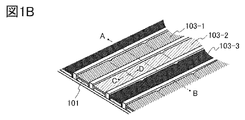


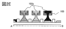


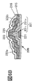


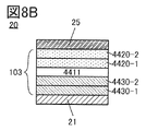

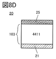


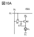


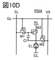

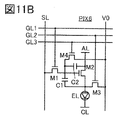


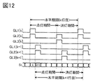


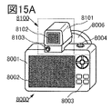

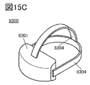
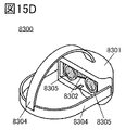


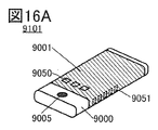

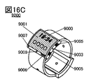


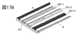


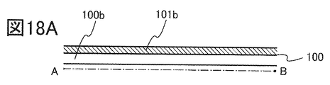
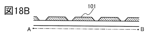


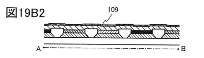
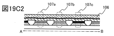


Classifications
-
- H—ELECTRICITY
- H10—SEMICONDUCTOR DEVICES; ELECTRIC SOLID-STATE DEVICES NOT OTHERWISE PROVIDED FOR
- H10K—ORGANIC ELECTRIC SOLID-STATE DEVICES
- H10K59/00—Integrated devices, or assemblies of multiple devices, comprising at least one organic light-emitting element covered by group H10K50/00
- H10K59/10—OLED displays
- H10K59/12—Active-matrix OLED [AMOLED] displays
- H10K59/122—Pixel-defining structures or layers, e.g. banks
-
- G—PHYSICS
- G09—EDUCATION; CRYPTOGRAPHY; DISPLAY; ADVERTISING; SEALS
- G09F—DISPLAYING; ADVERTISING; SIGNS; LABELS OR NAME-PLATES; SEALS
- G09F9/00—Indicating arrangements for variable information in which the information is built-up on a support by selection or combination of individual elements
- G09F9/30—Indicating arrangements for variable information in which the information is built-up on a support by selection or combination of individual elements in which the desired character or characters are formed by combining individual elements
-
- H—ELECTRICITY
- H05—ELECTRIC TECHNIQUES NOT OTHERWISE PROVIDED FOR
- H05B—ELECTRIC HEATING; ELECTRIC LIGHT SOURCES NOT OTHERWISE PROVIDED FOR; CIRCUIT ARRANGEMENTS FOR ELECTRIC LIGHT SOURCES, IN GENERAL
- H05B33/00—Electroluminescent light sources
- H05B33/12—Light sources with substantially two-dimensional radiating surfaces
- H05B33/14—Light sources with substantially two-dimensional radiating surfaces characterised by the chemical or physical composition or the arrangement of the electroluminescent material, or by the simultaneous addition of the electroluminescent material in or onto the light source
-
- H—ELECTRICITY
- H05—ELECTRIC TECHNIQUES NOT OTHERWISE PROVIDED FOR
- H05B—ELECTRIC HEATING; ELECTRIC LIGHT SOURCES NOT OTHERWISE PROVIDED FOR; CIRCUIT ARRANGEMENTS FOR ELECTRIC LIGHT SOURCES, IN GENERAL
- H05B33/00—Electroluminescent light sources
- H05B33/12—Light sources with substantially two-dimensional radiating surfaces
- H05B33/22—Light sources with substantially two-dimensional radiating surfaces characterised by the chemical or physical composition or the arrangement of auxiliary dielectric or reflective layers
-
- H—ELECTRICITY
- H10—SEMICONDUCTOR DEVICES; ELECTRIC SOLID-STATE DEVICES NOT OTHERWISE PROVIDED FOR
- H10K—ORGANIC ELECTRIC SOLID-STATE DEVICES
- H10K50/00—Organic light-emitting devices
-
- H—ELECTRICITY
- H10—SEMICONDUCTOR DEVICES; ELECTRIC SOLID-STATE DEVICES NOT OTHERWISE PROVIDED FOR
- H10K—ORGANIC ELECTRIC SOLID-STATE DEVICES
- H10K59/00—Integrated devices, or assemblies of multiple devices, comprising at least one organic light-emitting element covered by group H10K50/00
-
- H—ELECTRICITY
- H10—SEMICONDUCTOR DEVICES; ELECTRIC SOLID-STATE DEVICES NOT OTHERWISE PROVIDED FOR
- H10K—ORGANIC ELECTRIC SOLID-STATE DEVICES
- H10K59/00—Integrated devices, or assemblies of multiple devices, comprising at least one organic light-emitting element covered by group H10K50/00
- H10K59/80—Constructional details
- H10K59/805—Electrodes
- H10K59/8051—Anodes
- H10K59/80515—Anodes characterised by their shape
-
- H—ELECTRICITY
- H10—SEMICONDUCTOR DEVICES; ELECTRIC SOLID-STATE DEVICES NOT OTHERWISE PROVIDED FOR
- H10K—ORGANIC ELECTRIC SOLID-STATE DEVICES
- H10K59/00—Integrated devices, or assemblies of multiple devices, comprising at least one organic light-emitting element covered by group H10K50/00
- H10K59/30—Devices specially adapted for multicolour light emission
- H10K59/35—Devices specially adapted for multicolour light emission comprising red-green-blue [RGB] subpixels
Definitions
- One embodiment of the present invention relates to an organic compound, a light-emitting element, a light-emitting device, a display module, a lighting module, a display device, a light-emitting device, an electronic device, a lighting device, and an electronic device.
- a technical field of one embodiment of the invention disclosed in this specification and the like relates to a product, a method, or a manufacturing method.
- one aspect of the invention relates to a process, machine, manufacture, or composition of matter.
- the technical field of one embodiment of the present invention disclosed in this specification more specifically includes semiconductor devices, display devices, liquid crystal display devices, light-emitting devices, lighting devices, power storage devices, storage devices, imaging devices, and the like. Driving methods or their manufacturing methods can be mentioned as an example.
- Light-emitting devices (organic EL devices) utilizing electroluminescence (EL) using organic compounds have been put to practical use.
- the basic structure of these light-emitting devices is to sandwich an organic compound layer (EL layer) containing a light-emitting material between a pair of electrodes.
- EL layer organic compound layer
- Such a light-emitting device is self-luminous, when it is used as a pixel of a display, it has advantages such as high visibility and no need for a backlight, and is particularly suitable for a flat panel display. Another great advantage of a display using such a light-emitting device is that it can be made thin and light. Another feature is its extremely fast response speed.
- An object of one embodiment of the present invention is to provide a light-emitting device with high display quality.
- an object of one embodiment of the present invention is to provide an inexpensive light-emitting device.
- an object of one embodiment of the present invention is to provide a light-emitting device with high emission efficiency.
- an object of one embodiment of the present invention is to provide a light-emitting device that is inexpensive and has good display quality.
- the present invention should solve any one of the above problems.
- a plurality of partition walls formed over an insulating surface and extending in a first direction, a plurality of island-shaped pixel electrodes formed over the insulating surface, and and a second electrode provided on the EL layer.
- the pixel electrodes aligned in one direction are arranged one by one, and the EL layer is formed on the insulating surface between the pixel electrodes adjacent to each other in the first direction among the pixel electrodes aligned in the first direction. It is a light-emitting device that is in contact with the
- one embodiment of the present invention includes a plurality of partition walls formed over an insulating surface and extending in a first direction, a plurality of island-shaped pixel electrodes formed over the insulating surface, and and a second electrode provided on the EL layer, the partition wall has an insulating property, and between the partition walls adjacent to each other in the plurality of partition walls, The pixel electrodes aligned in the first direction are arranged one by one, and the ends of the pixel electrodes substantially parallel to the first direction are covered with the partition walls and aligned in the first direction.
- the EL layer is in contact with the insulating surface between the pixel electrodes adjacent to each other in the first direction.
- the EL layer is provided continuously over the pixel electrodes aligned in the first direction.
- the light-emitting device has a plurality of columns of the pixel electrodes aligned in the first direction, and is positioned between adjacent columns of the pixel electrodes.
- the partition wall is a single light emitting device.
- the layers from the layer in contact with the pixel electrode to the light-emitting layer in the EL layer are independent for each column of the pixel electrodes aligned in the first direction. It is a light-emitting device that
- another embodiment of the present invention is a light-emitting device having the above structure, in which EL layers included in the adjacent columns of pixel electrodes contain different light-emitting materials.
- the light emitting device has at least three columns of the pixel electrodes aligned in the first direction, and among the three columns of the pixel electrodes, An EL layer formed on one of the pixel electrodes in one column contains a light-emitting material that emits red light, and is formed on one of the pixel electrodes in the other two columns.
- the EL layer contains a light-emitting material that emits green light
- the EL layer formed over the pixel electrodes in the other column contains a light-emitting material that emits blue light.
- another embodiment of the present invention is a light-emitting device having the above structure, in which portions of the EL layer that are independent for each column of the pixel electrodes are formed by a droplet discharge method.
- another embodiment of the present invention is the light-emitting device having the above structure, in which part of the EL layer is continuous over the pixel electrodes in different columns.
- the EL layer is a light-emitting device in which the electron-transporting layer and/or the electron-injecting layer are continuous over the pixel electrodes in different columns.
- another embodiment of the present invention is the light-emitting device having the above structure, in which the second electrode is provided continuously over the plurality of pixel electrodes.
- another embodiment of the present invention is a light-emitting device having the above structure, in which at least part of an end portion of the pixel electrode has a tapered shape.
- an end portion when the pixel electrode is cut along a plane substantially perpendicular to the insulating surface, an end portion has a portion with an angle of 5 degrees or more and 90 degrees or less. It is a light emitting device.
- another embodiment of the present invention is a display device including any of the above light-emitting devices.
- another embodiment of the present invention is an electronic device including any of the above light-emitting devices, a sensor, an operation button, and a speaker or a microphone.
- another aspect of the present invention is a lighting device including any one of the light-emitting devices described above and a housing.
- the light-emitting device in this specification includes an image display device using a light-emitting device.
- a module in which a connector such as an anisotropic conductive film or TCP (Tape Carrier Package) is attached to the light emitting device a module in which a printed wiring board is provided at the end of the TCP, or a COG (Chip On Glass) method for the light emitting device
- the light-emitting device may also include a module in which an IC (integrated circuit) is directly mounted. Additionally, lighting fixtures and the like may have light emitting devices.
- One embodiment of the present invention can provide a light-emitting device with high display quality.
- an inexpensive light-emitting device can be provided.
- a light-emitting device with high emission efficiency can be provided.
- a light-emitting device with high display quality can be provided at low cost.
- FIG. 1A, 1B, 1C and 1D are perspective and cross-sectional views of a light emitting device.
- 2A to 2F are cross-sectional views showing manufacturing steps of the light-emitting device.
- 3A1, 3A2, 3B2, and 3C2 are cross-sectional views showing manufacturing steps of the light emitting device.
- FIG. 4 is a perspective view of the light emitting device.
- 5A and 5B are cross-sectional views of the light emitting device.
- 6A and 6B are cross-sectional views of the light emitting device.
- FIG. 7 is a cross-sectional view of the light emitting device.
- 8A-8E are cross-sectional views of light emitting devices.
- FIG. 9 is a conceptual diagram for explaining a droplet discharge device.
- 10A to 10D are circuit diagrams of light emitting devices.
- 11A to 11D are circuit diagrams of the light emitting device.
- FIG. 12 is a timing chart of the light emitting device.
- 13A and 13B are diagrams illustrating examples of electronic devices.
- 14A to 14D are diagrams illustrating examples of electronic devices.
- 15A to 15F are diagrams illustrating examples of electronic devices.
- 16A to 16F are diagrams illustrating examples of electronic devices.
- 17A, 17B, 17C and 17D are perspective and cross-sectional views of the light emitting device.
- 18A to 18F are cross-sectional views showing manufacturing steps of a light-emitting device.
- 19A1, 19A2, 19B2, and 19C2 are cross-sectional views showing manufacturing steps of the light-emitting device.
- 20A and 20B are cross-sectional views of the light emitting device.
- 21A and 21B are cross-sectional views of the light emitting device.
- FIG. 22 is a cross
- a device manufactured using a metal mask or FMM may be referred to as a device with an MM (metal mask) structure.
- a device manufactured without using a metal mask or FMM may be referred to as a device with an MML (metal maskless) structure.
- a light-emitting device of one embodiment of the present invention includes a plurality of pixel electrodes 101 and a plurality of partition walls 102 over an insulating surface 100 .
- the partitions 102 are formed to extend in the first direction, and a plurality of pixel electrodes 101 (eg, pixel electrodes 101) aligned in the first direction between adjacent partitions 102 (eg, partitions 102-1 and 102-2). 101-1, pixel electrode 101-2 and pixel electrode 101-3) are located.
- a plurality of columns of pixel electrodes 101 aligned in the first direction are formed in the light-emitting device as shown in the drawing, and partition walls 102 exist between the columns of pixel electrodes 101 .
- the EL layer 103 is provided on the pixel electrode 101 (see FIG. 1B).
- the EL layer 103 contains a light-emitting material and has a structure in which light emission can be obtained from the light-emitting material by current excitation.
- the EL layer 103 is preferably manufactured by a wet method, particularly a droplet discharge method such as an inkjet method or a nozzle printing method.
- the EL layer 103 is easily formed by forming the EL layer 103 while moving the nozzle in the first direction by a droplet discharging method. can do.
- the composition (also referred to as ink) discharged by the partitions 102 can be prevented from flowing out to the columns of the different pixel electrodes. Ink can be prevented from leaking onto adjacent pixel electrodes in a direction perpendicular to the line.
- the EL layer 103 is preferably formed continuously over a plurality of pixel electrodes over the pixel electrodes 101 aligned in the first direction.
- the EL layer 103 can be formed continuously in the first direction by moving the nozzle in the first direction by a droplet discharging method.
- the EL layer 103 has a portion 104 indicated by a circle in FIG. It has a portion where the insulating surface 100 and the EL layer 103 are in contact with each other.
- the partition 102 does not exist between the pixel electrodes aligned in the first direction.
- the film thickness may be a region where the film thickness gradually increases from the inner side of the pixel electrode toward the partition wall. If the thickness of the EL layer is different, the brightness of that portion is lowered, and the light emitting region does not function effectively. In addition, the concentration of the electric field on the thin portion of the film may also be caused, which may adversely affect the service life.
- the effective light-emitting area can be increased; thus, the aperture ratio is high. , it becomes easy to obtain a light-emitting device with low power consumption.
- the light-emitting device can have excellent display quality.
- the light-emitting device can have a long life.
- the light-emitting device of one embodiment of the present invention has a structure in which the latter method for separate painting (also referred to as a side-by-side method) can be easily achieved.
- an EL layer 103 exhibiting a different emission color for each column of pixel electrodes, and an EL layer 103 containing a luminescent material having a different emission color is formed in adjacent columns of pixel electrodes.
- layer 103 is formed.
- the EL layer 103 containing a light-emitting material that emits red light in the EL layer 103-1, green light in the EL layer 103-2, and blue light in the EL layer 103-3.
- the EL layer 103 is formed by a droplet discharging method from the pixel electrode side to the light emitting layer, that is, the layer containing the light emitting material, and the subsequent carrier transport layer and/or carrier injection layer is formed on the pixel electrodes in different columns. may be formed in common over At this time, the carrier transport layer and/or the carrier injection layer may be formed by other wet methods such as spin coating, or may be formed by dry methods such as vacuum deposition. Also, the second electrode may be common between the light emitting devices having different columns of pixel electrodes.
- the carrier transport layer and/or the carrier injection layer become the electron transport layer and/or the electron injection layer
- the hole transport layer and/or the hole injection layer it is preferable that the pixel electrode formed first is an anode because it is easy to manufacture.
- a method for manufacturing a light-emitting device of one embodiment of the present invention is described.
- a conductive film 101b is formed on an insulator 100b having an insulating surface 100 (FIG. 2A).
- the pixel electrode 101 is formed by patterning the conductive film 101b (FIG. 2B).
- the edge of the pixel electrode 101 may have a tapered shape.
- a tapered shape refers to a shape in which at least a part of the side surface of the structure is inclined with respect to the substrate surface.
- the angle formed by the inclined side surface and the substrate surface is preferably 5 degrees to 90 degrees.
- an insulating film 102b is formed to cover the insulating surface 100 and the pixel electrode 101 (FIG. 2C).
- the insulating film 102b may be an organic compound or an inorganic compound.
- the partition walls 102 are formed by patterning the insulating film (FIG. 2D).
- the partition 102 is formed between the pixel electrodes 101 and 101 .
- the EL layer material 105b is discharged from the nozzle using the droplet discharge method (FIG. 2E).
- the material of the EL layer 103 can be arranged between the partitions over the pixel electrodes by continuously ejecting the material while the nozzle moves in the first direction (depth direction of the screen). It is preferable to discharge droplets continuously in the first direction instead of pixel by pixel. At this time, by using a plurality of nozzles and coating a plurality of rows of pixel electrodes at the same time, manufacturing efficiency can be improved.
- the ejected material 105b can be processed for solvent removal or curing to form the EL layers 103 (EL layer 103-1, EL layer 103-2, EL layer 103-3) (FIG. 2F).
- the light emitting device 107 (107a, 107b, 107c) can be produced by forming the second electrode 106 as shown in FIG. 3A1.
- the operations of FIGS. 2E and 2F are repeated.
- an EL layer 103 can be formed, and then a light-emitting device 107 can be manufactured by forming a second electrode 106 as shown in FIG. 3A1. Details of FIGS. 8A to 8C will be described later.
- At least the layers from the pixel electrode 101 to the layer containing a light-emitting material are formed by a droplet discharge method; however, layers to be formed after that may be formed by any method. Therefore, after forming layers up to the layer containing the light-emitting material by the droplet discharge method, as shown in FIGS.
- a light-emitting device 107 can also be fabricated by forming a second electrode 106 (FIG. 3C2). In this case, since the formation of the common layer is completed only once, the manufacturing process is simplified and the configuration is favorable in terms of cost. Note that FIGS.
- 3A2 and 3B2 show a structure in which a carrier transport layer and a carrier injection layer are respectively formed, but either one of them may be formed as a common layer, or a layer having both functions may be formed. can be Moreover, you may form functional layers other than these.
- a protective layer is formed over the second electrode, and sealing is performed with a counter substrate provided with a light-blocking layer or the like, whereby a light-emitting device of one embodiment of the present invention can be manufactured. Note that by connecting the light-emitting device 107 to a driving transistor, display of each pixel can be controlled, and a light-emitting device with high display quality can be obtained.
- a light-emitting device of one embodiment of the present invention includes a plurality of pixel electrodes 101 and a plurality of partition walls 102 over an insulating surface 100 .
- the partitions 102 are formed to extend in the first direction, and a plurality of pixel electrodes 101 (eg, pixel electrodes 101) aligned in the first direction between adjacent partitions 102 (eg, partitions 102-1 and 102-2). 101-1, pixel electrode 101-2 and pixel electrode 101-3) are exposed.
- a plurality of columns of pixel electrodes 101 aligned in the first direction are formed in the light-emitting device as shown in the drawing, and partition walls 102 exist between the columns of pixel electrodes 101 . 1 to 3 in that the partition 102 is formed so as to cover a pair of sides of the pixel electrode, but other configurations are the same as those in FIGS.
- FIG. 4 shows an external perspective view of a light-emitting device of one embodiment of the present invention
- FIG. 5 shows a cross-sectional view of a light-emitting device of one embodiment of the present invention having a light-emitting device connected to a transistor.
- the light emitting device 400A has a configuration in which a substrate 452 and a substrate 451 are bonded together.
- the substrate 452 is clearly indicated by dashed lines.
- the light emitting device 400A has a display section 462, a circuit 464, wiring 465, and the like.
- FIG. 4 shows an example in which an IC 473 and an FPC 472 are mounted on the light emitting device 400A. Therefore, the configuration shown in FIG. 4 can also be said to be a display module including the light emitting device 400A, an IC (integrated circuit), and an FPC.
- a scanning line driving circuit for example, can be used as the circuit 464 .
- the wiring 465 has a function of supplying signals and power to the display section 462 and the circuit 464 .
- the signal and power are input to the wiring 465 from the outside through the FPC 472 or input to the wiring 465 from the IC 473 .
- FIG. 4 shows an example in which an IC 473 is provided on a substrate 451 by a COG (Chip On Glass) method, a COF (Chip on Film) method, or the like.
- a COG Chip On Glass
- COF Chip on Film
- the IC 473 for example, an IC having a scanning line driver circuit, a signal line driver circuit, or the like can be applied.
- the light emitting device 400A and the display module may be configured without an IC.
- the IC may be mounted on the FPC by the COF method or the like.
- 5A and 20A show cross sections of the light-emitting device 400A, part of the region including the FPC 472, part of the circuit 464, part of the display part 462, and part of the region including the end. shows an example of
- 5A and 20A includes a transistor 201 and a transistor 205, a light emitting device 430a that emits red light, a light emitting device 430b that emits green light, and a light emitting device 430b that emits blue light. It has a light-emitting device 430c and the like that emits .
- the light emitting device 430a, the light emitting device 430b, and the light emitting device 430c correspond to the light emitting device 107a, the light emitting device 107b, and the light emitting device 107c.
- the three sub-pixels are R, G, and B sub-pixels, and yellow (Y). , cyan (C), and magenta (M).
- the four sub-pixels include R, G, B, and white (W) sub-pixels, and R, G, B, and Y four-color sub-pixels. be done.
- the protective layer 416 and the substrate 452 are adhered via the adhesive layer 442 .
- a solid sealing structure, a hollow sealing structure, or the like can be applied to sealing the light-emitting device.
- 5A and 20A, the space 443 surrounded by the substrate 452, the adhesion layer 442, and the substrate 451 is filled with an inert gas (such as nitrogen or argon) to apply a hollow sealing structure.
- the adhesive layer 442 may be provided overlying the light emitting device.
- a space 443 surrounded by the substrate 452 , the adhesive layer 442 , and the substrate 451 may be filled with a resin different from that of the adhesive layer 442 .
- the light-emitting devices 430a, 430b, and 430c may have an optical adjustment layer 426a, an optical adjustment layer 426b, and an optical adjustment layer 426c between the pixel electrode and the EL layer.
- the optical adjustment layers 426 (426a, 426b, and 426c) are provided as part of the electrodes in FIGS. 5A and 20A, they may also be provided inside the EL layer as a carrier transport layer.
- the pixel electrodes 411a, 411b, and 411c are connected to the conductive layer 222b of the transistor 205 through openings provided in the insulating layer 214, respectively.
- the pixel electrode contains a material that reflects visible light
- the counter electrode contains a material that transmits visible light
- the light emitted by the light emitting device is emitted to the substrate 452 side.
- a material having high visible light transmittance is preferably used for the substrate 452 .
- Both the transistor 201 and the transistor 205 are formed over the substrate 451 . These transistors can be made with the same material and the same process.
- An insulating layer 211, an insulating layer 213, an insulating layer 215, and an insulating layer 214 are provided on the substrate 451 in this order.
- Part of the insulating layer 211 functions as a gate insulating layer of each transistor.
- Part of the insulating layer 213 functions as a gate insulating layer of each transistor.
- An insulating layer 215 is provided over the transistor.
- An insulating layer 214 is provided over the transistor and functions as a planarization layer. Note that the number of gate insulating layers and the number of insulating layers covering a transistor are not limited, and each may have a single layer or two or more layers.
- a material in which impurities such as water and hydrogen are difficult to diffuse for at least one insulating layer covering the transistor.
- Inorganic insulating films are preferably used for the insulating layer 211, the insulating layer 213, and the insulating layer 215, respectively.
- As the inorganic insulating film for example, a silicon nitride film, a silicon oxynitride film, a silicon oxide film, a silicon oxynitride film, an aluminum oxide film, an aluminum nitride film, or the like can be used.
- a hafnium oxide film, an yttrium oxide film, a zirconium oxide film, a gallium oxide film, a tantalum oxide film, a magnesium oxide film, a lanthanum oxide film, a cerium oxide film, a neodymium oxide film, or the like may be used.
- two or more of the insulating films described above may be laminated and used.
- An organic insulating film is suitable for the insulating layer 214 that functions as a planarizing layer.
- materials that can be used for the organic insulating film include acrylic resins, polyimide resins, epoxy resins, polyamide resins, polyimideamide resins, siloxane resins, benzocyclobutene-based resins, phenolic resins, precursors of these resins, and the like.
- the organic insulating film preferably has openings near the ends of the light emitting device 400A. As a result, it is possible to prevent impurities from entering through the organic insulating film from the end of the light emitting device 400A.
- the organic insulating film may be formed so that the ends of the organic insulating film are located inside the ends of the light emitting device 400A so that the organic insulating film is not exposed at the ends of the light emitting device 400A.
- An opening is formed in the insulating layer 214 in a region 228 shown in FIGS. 5A and 20A. As a result, even when an organic insulating film is used for the insulating layer 214 , it is possible to prevent impurities from entering the display section 462 from the outside through the insulating layer 214 . Therefore, the reliability of the light emitting device 400A can be improved.
- a conductive layer 221 functioning as a gate electrode an insulating layer 211 functioning as a gate insulating layer, conductive layers 222a and 222b functioning as sources and drains, a semiconductor layer 231, and a gate insulating layer. It has an insulating layer 213 and a conductive layer 223 functioning as a gate.
- the same hatching pattern is applied to a plurality of layers obtained by processing the same conductive film.
- the insulating layer 211 is located between the conductive layer 221 and the semiconductor layer 231 .
- the insulating layer 213 is located between the conductive layer 223 and the semiconductor layer 231 .
- the insulating layer 421 is located between pixel electrodes and functions as a partition separating pixels of different emission colors.
- the insulating layer 421 corresponds to the partition 102 in FIGS. 1 and 17.
- the structure of the transistor included in the display device of this embodiment there is no particular limitation on the structure of the transistor included in the display device of this embodiment.
- a planar transistor, a staggered transistor, an inverted staggered transistor, or the like can be used.
- the transistor structure may be either a top-gate type or a bottom-gate type.
- gates may be provided above and below a semiconductor layer in which a channel is formed.
- a structure in which a semiconductor layer in which a channel is formed is sandwiched between two gates is applied to the transistors 201 and 205 .
- a transistor may be driven by connecting two gates and applying the same signal to them.
- the threshold voltage of the transistor may be controlled by applying a potential for controlling the threshold voltage to one of the two gates and applying a potential for driving to the other.
- the crystallinity of the semiconductor material used for the transistor is not particularly limited, either. (semiconductors having A single crystal semiconductor or a crystalline semiconductor is preferably used because deterioration in transistor characteristics can be suppressed.
- a semiconductor layer of a transistor preferably includes a metal oxide (also referred to as an oxide semiconductor).
- the display device of this embodiment preferably uses a transistor including a metal oxide for a channel formation region (hereinafter referred to as an OS transistor).
- the semiconductor layer of the transistor may comprise silicon. Examples of silicon include amorphous silicon and crystalline silicon (low-temperature polysilicon, monocrystalline silicon, etc.).
- Transistors containing silicon in a semiconductor layer are preferably used for the transistors 201 and 205 .
- Examples of silicon include monocrystalline silicon, polycrystalline silicon, amorphous silicon, and the like.
- a transistor including low-temperature polysilicon (LTPS) in a semiconductor layer hereinafter also referred to as an LTPS transistor.
- the LTPS transistor has high field effect mobility and can operate at high speed.
- M is gallium, aluminum, silicon, boron, yttrium, tin, copper, vanadium, beryllium, titanium, iron, nickel, germanium, zirconium, molybdenum, lanthanum, cerium , neodymium, hafnium, tantalum, tungsten, and magnesium
- M is preferably one or more selected from aluminum, gallium, yttrium, and tin
- the semiconductor layer contains an oxide containing indium (In), gallium (Ga), and zinc (Zn) (IGZO (also referred to as ) is preferably used.
- the atomic ratio of In in the In-M-Zn oxide is preferably equal to or higher than the atomic ratio of M.
- the above transistor including LTPS in the semiconductor layer and the above transistor including IGZO in the semiconductor layer may be used in combination.
- a transistor including LTPS in a semiconductor layer and a transistor including IGZO in a semiconductor layer in combination a display device can have a high-speed operation function and a low power consumption function.
- the transistor included in the circuit 464 and the transistor included in the display portion 462 may have the same structure or different structures.
- the plurality of transistors included in the circuit 464 may all have the same structure, or may have two or more types.
- the plurality of transistors included in the display portion 462 may all have the same structure, or may have two or more types.
- a connecting portion 204 is provided in a region of the substrate 451 where the substrate 452 does not overlap.
- the wiring 465 is electrically connected to the FPC 472 through the conductive layer 466 and the connection layer 242 .
- the conductive layer 466 shows an example of a laminated structure of a conductive film obtained by processing the same conductive film as the pixel electrode and a conductive film obtained by processing the same conductive film as the optical adjustment layer. .
- the conductive layer 466 is exposed on the upper surface of the connecting portion 204 . Thereby, the connecting portion 204 and the FPC 472 can be electrically connected via the connecting layer 242 .
- a light shielding layer 417 is preferably provided on the surface of the substrate 452 on the substrate 451 side.
- various optical members can be arranged outside the substrate 452 .
- optical members include polarizing plates, retardation plates, light diffusion layers (diffusion films, etc.), antireflection layers, light collecting films, and the like.
- an antistatic film that suppresses adhesion of dust, a water-repellent film that prevents adhesion of dirt, a hard coat film that suppresses the occurrence of scratches due to use, a shock absorption layer, etc. are arranged on the outside of the substrate 452.
- an antistatic film that suppresses adhesion of dust, a water-repellent film that prevents adhesion of dirt, a hard coat film that suppresses the occurrence of scratches due to use, a shock absorption layer, etc. are arranged.
- the protective layer 416 that covers the light-emitting device By providing the protective layer 416 that covers the light-emitting device, it is possible to prevent impurities such as water from entering the light-emitting device and improve the reliability of the light-emitting device.
- the insulating layer 215 and the protective layer 416 are in contact with each other through the opening of the insulating layer 214 in the region 228 near the edge of the light emitting device 400A.
- the inorganic insulating film included in the insulating layer 215 and the inorganic insulating film included in the protective layer 416 are preferably in contact with each other. This can prevent impurities from entering the display section 462 from the outside through the organic insulating film. Therefore, the reliability of the light emitting device 400A can be improved.
- 5B and 20B show examples in which the protective layer 416 has a three-layer structure.
- the protective layer 416 has an inorganic insulating layer 416a over the light emitting device 430c, an organic insulating layer 416b over the inorganic insulating layer 416a, and an inorganic insulating layer 416c over the organic insulating layer 416b.
- the end of the inorganic insulating layer 416a and the end of the inorganic insulating layer 416c extend outside the end of the organic insulating layer 416b and are in contact with each other.
- the inorganic insulating layer 416a is in contact with the insulating layer 215 (inorganic insulating layer) through the opening of the insulating layer 214 (organic insulating layer).
- the light emitting device can be surrounded by the insulating layer 215 and the protective layer 416, so that the reliability of the light emitting device can be improved.
- the protective layer 416 may have a laminated structure of an organic insulating film and an inorganic insulating film. At this time, it is preferable that the end portion of the inorganic insulating film extends further outward than the end portion of the organic insulating film.
- the substrates 451 and 452 glass, quartz, ceramics, sapphire, resins, metals, alloys, semiconductors, etc. can be used, respectively.
- a material that transmits the light is used for the substrate on the side from which the light from the light-emitting device is extracted.
- the flexibility of the display device can be increased.
- a polarizing plate may be used as the substrate 451 or the substrate 452 .
- polyester resins such as polyethylene terephthalate (PET) and polyethylene naphthalate (PEN), polyacrylonitrile resins, acrylic resins, polyimide resins, polymethylmethacrylate resins, polycarbonate (PC) resins, and polyether resins are used, respectively.
- PES resin Sulfone (PES) resin, polyamide resin (nylon, aramid, etc.), polysiloxane resin, cycloolefin resin, polystyrene resin, polyamideimide resin, polyurethane resin, polyvinyl chloride resin, polyvinylidene chloride resin, polypropylene resin, polytetrafluoroethylene (PTFE) resin, ABS resin, cellulose nanofiber, or the like can be used.
- PES polytetyrene resin
- polyamideimide resin polyurethane resin
- polyvinyl chloride resin polyvinylidene chloride resin
- polypropylene resin polytetrafluoroethylene (PTFE) resin
- PTFE resin polytetrafluoroethylene
- ABS resin cellulose nanofiber, or the like
- One or both of the substrates 451 and 452 may be made of glass having a thickness sufficient to be flexible.
- a substrate having high optical isotropy has small birefringence (it can be said that the amount of birefringence is small).
- the absolute value of the retardation (retardation) value of the substrate with high optical isotropy is preferably 30 nm or less, more preferably 20 nm or less, and even more preferably 10 nm or less.
- Films with high optical isotropy include triacetylcellulose (TAC, also called cellulose triacetate) films, cycloolefin polymer (COP) films, cycloolefin copolymer (COC) films, and acrylic films.
- TAC triacetylcellulose
- COP cycloolefin polymer
- COC cycloolefin copolymer
- a film having a low water absorption rate as the substrate.
- various curable adhesives such as photocurable adhesives such as ultraviolet curable adhesives, reaction curable adhesives, thermosetting adhesives, and anaerobic adhesives can be used.
- These adhesives include epoxy resins, acrylic resins, silicone resins, phenol resins, polyimide resins, imide resins, PVC (polyvinyl chloride) resins, PVB (polyvinyl butyral) resins, EVA (ethylene vinyl acetate) resins, and the like.
- a material with low moisture permeability such as epoxy resin is preferable.
- a two-liquid mixed type resin may be used.
- an adhesive sheet or the like may be used.
- connection layer 242 an anisotropic conductive film (ACF), an anisotropic conductive paste (ACP), or the like can be used.
- ACF anisotropic conductive film
- ACP anisotropic conductive paste
- materials that can be used for conductive layers such as various wirings and electrodes constituting display devices include aluminum, titanium, chromium, nickel, copper, yttrium, zirconium, molybdenum, silver, Examples include metals such as tantalum and tungsten, and alloys containing these metals as main components. A film containing these materials can be used as a single layer or as a laminated structure.
- conductive oxides such as indium oxide, indium tin oxide, indium zinc oxide, zinc oxide, zinc oxide containing gallium, or graphene can be used.
- metal materials such as gold, silver, platinum, magnesium, nickel, tungsten, chromium, molybdenum, iron, cobalt, copper, palladium, and titanium, or alloy materials containing such metal materials can be used.
- a nitride of the metal material eg, titanium nitride
- it is preferably thin enough to have translucency.
- a stacked film of any of the above materials can be used as the conductive layer.
- a laminated film of a silver-magnesium alloy and indium tin oxide because the conductivity can be increased.
- conductive layers such as various wirings and electrodes that constitute a display device, and conductive layers (conductive layers functioning as pixel electrodes or common electrodes) of light-emitting devices.
- Examples of insulating materials that can be used for each insulating layer include resins such as acrylic resins and epoxy resins, and inorganic insulating materials such as silicon oxide, silicon oxynitride, silicon nitride oxide, silicon nitride, and aluminum oxide.
- FIGS. 6A and 21A show cross-sectional views of the light emitting device 400B.
- FIG. 6A has a light emitting device having the configuration shown in FIG. 1 and FIG. 21A having the configuration shown in FIG.
- a perspective view of the light emitting device 400B is the same as that of the light emitting device 400A (FIG. 4).
- 6A and 21A show an example of a cross section of the light emitting device 400B when part of the region including the FPC 472, part of the circuit 464, and part of the display section 462 are cut.
- 6A and 21A show an example of a cross section of the display section 462, in particular when a region including the light emitting device 430b emitting green light and the light emitting device 430c emitting blue light is cut. Note that the description of the same parts as those of the light emitting device 400A may be omitted.
- a light-emitting device 400B shown in FIGS. 6A and 21A has a transistor 202, a transistor 210, a light-emitting device 430b, a light-emitting device 430c, and the like between a substrate 453 and a substrate 454.
- FIG. 1 A light-emitting device 400B shown in FIGS. 6A and 21A has a transistor 202, a transistor 210, a light-emitting device 430b, a light-emitting device 430c, and the like between a substrate 453 and a substrate 454.
- the substrate 454 and the protective layer 416 are adhered via the adhesive layer 442 .
- the adhesive layer 442 is overlapped with each of the light emitting device 430b and the light emitting device 430c, and a solid sealing structure is applied to the light emitting device 400B.
- the substrate 453 and the insulating layer 212 are bonded together by an adhesive layer 455 .
- the light-emitting device 400B As a method for manufacturing the light-emitting device 400B, first, a manufacturing substrate on which the insulating layer 212, each transistor, each light-emitting device, etc. are provided and the substrate 454 on which the light shielding layer 417 is provided are bonded together by the adhesive layer 442. Then, the formation substrate is peeled off and a substrate 453 is attached to the exposed surface, so that each component formed over the formation substrate is transferred to the substrate 453 .
- Each of the substrates 453 and 454 preferably has flexibility. This can enhance the flexibility of the light emitting device 400B.
- Inorganic insulating films that can be used for the insulating layers 211, 213, and 215 can be used for the insulating layer 212, respectively.
- the pixel electrode is connected to the conductive layer 222b of the transistor 210 through an opening provided in the insulating layer 214.
- the conductive layer 222 b is connected to the low-resistance region 231 n through openings provided in the insulating layers 215 and 225 .
- the transistor 210 has the function of controlling driving of the light emitting device.
- the light emitted by the light emitting devices 430b and 430c is emitted to the substrate 454 side.
- a material having high visible light transmittance is preferably used for the substrate 454 .
- a connecting portion 204 is provided in a region of the substrate 453 where the substrate 454 does not overlap.
- the wiring 465 is electrically connected to the FPC 472 through the conductive layer 466 and the connection layer 242 .
- the conductive layer 466 can be obtained by processing the same conductive film as the pixel electrode. Thereby, the connecting portion 204 and the FPC 472 can be electrically connected via the connecting layer 242 .
- the transistors 202 and 210 each include a conductive layer 221 functioning as a gate, an insulating layer 211 functioning as a gate insulating layer, a semiconductor layer having a channel formation region 231i and a pair of low-resistance regions 231n, and one of the pair of low-resistance regions 231n.
- a connecting conductive layer 222a, a conductive layer 222b connecting to the other of the pair of low-resistance regions 231n, an insulating layer 225 functioning as a gate insulating layer, a conductive layer 223 functioning as a gate, and an insulating layer 215 covering the conductive layer 223 are provided.
- the insulating layer 211 is located between the conductive layer 221 and the channel formation region 231i.
- the insulating layer 225 is located between the conductive layer 223 and the channel formation region 231i.
- the conductive layers 222a and 222b are each connected to the low resistance region 231n through openings provided in the insulating layer 215.
- One of the conductive layers 222a and 222b functions as a source and the other functions as a drain.
- 6A and 21A show examples in which the insulating layer 225 covers the top and side surfaces of the semiconductor layer.
- the conductive layers 222a and 222b are connected to the low-resistance region 231n through openings provided in the insulating layers 225 and 215, respectively.
- the insulating layer 225 overlaps the channel formation region 231i of the semiconductor layer 231 and does not overlap the low resistance region 231n.
- the insulating layer 225 is provided to cover the insulating layer 225 and the conductive layer 223, and the conductive layers 222a and 222b are connected to the low resistance region 231n through openings in the insulating layer 215, respectively.
- an insulating layer 218 may be provided to cover the transistor.
- FIG. 7 and 22 show cross-sectional views of the light emitting device 400C.
- FIG. 7 has the light emitting device having the configuration shown in FIG. 1 and
- FIG. 22 has the configuration shown in FIG.
- a perspective view of the light emitting device 400C is the same as that of the light emitting device 400A (FIG. 4).
- 7 and 22 show examples of cross sections of the light emitting device 400C when part of the region including the FPC 472, part of the circuit 464, and part of the display section 462 are cut. Note that the description of the same parts as those of the light emitting device 400A may be omitted.
- the pixel electrodes 411a to 411c are formed using a light-transmitting conductive material. Also, the second electrode is a reflective electrode.
- the light-emitting device 400 ⁇ /b>C having such a configuration becomes a bottom-emission light-emitting device in which light emitted from the light-emitting device is emitted toward the substrate 451 .
- the transistor is formed using an oxide semiconductor and each electrode of the transistor is formed using a light-transmitting material, light is less likely to be blocked even if the transistor is provided on an optical path through which light from the light-emitting device is emitted to the outside. Therefore, a high-definition light-emitting device with a large aperture ratio can be obtained.
- This embodiment can be implemented by appropriately combining at least part of it with other embodiments described herein.
- the light emitting device has an EL layer 103 between a pair of electrodes (lower electrode 21, upper electrode 25).
- the EL layer 103 included in the light-emitting device can be composed of a plurality of layers such as the layer 4420, the light-emitting layer 4411, and the layer 4430.
- the layer 4420 can have, for example, a layer containing a substance with high electron-injection properties (electron-injection layer) and a layer containing a substance with high electron-transport properties (electron-transporting layer).
- the light-emitting layer 4411 contains, for example, a light-emitting compound.
- Layer 4430 can have, for example, a layer containing a substance with high hole-injection properties (hole-injection layer) and a layer containing a substance with high hole-transport properties (hole-transport layer).
- FIG. 8B is a modification of the EL layer 103 included in the light emitting device 20 shown in FIG. 8A.
- the light-emitting device 20 shown in FIG. It has a layer 4420-1 on 4411, a layer 4420-2 on layer 4420-1, and an upper electrode 25 on layer 4420-2.
- the layer 4430-1 functions as a hole injection layer
- the layer 4430-2 functions as a hole transport layer
- the layer 4420-1 functions as an electron Functioning as a transport layer
- layer 4420-2 functions as an electron injection layer.
- layer 4430-1 functions as an electron injection layer
- layer 4430-2 functions as an electron transport layer
- layer 4420-1 functions as a hole transport layer.
- layer, with layer 4420-2 functioning as the hole injection layer With such a layer structure, carriers can be efficiently injected into the light-emitting layer 4411 and the efficiency of carrier recombination in the light-emitting layer 4411 can be increased.
- the layer included between the light-emitting layer 4411 and the lower electrode 21 and the layer included between the light-emitting layer 4411 and the upper electrode 25 are not limited to these. good.
- a layer having both functions of a carrier transport layer and a carrier injection layer may be used.
- FIG. 8C Another variation is a configuration in which a plurality of light-emitting layers (light-emitting layers 4411, 4412, and 4413) are provided between layers 4420 and 4430 as shown in FIG. 8C.
- White light emission can be easily obtained from the light-emitting device 20 by using different light-emitting materials in a plurality of light-emitting layers (for example, each light-emitting layer includes materials that emit red, green, and blue light). It becomes possible.
- FIG. 8C shows a configuration in which there are three light-emitting layers, the number of light-emitting layers may be two or four or more.
- the layers 4420 and 4430 may have a laminated structure composed of two or more layers.
- FIG. 8D shows a modification of the EL layer 103 included in the light emitting device 20.
- the EL layer 103 is composed of a single light-emitting layer 4411 containing a light-emitting material.
- Examples include a structure in which the light-emitting layer 4411 is formed by using a light-emitting layer 4411 and a structure in which the light-emitting layer 4411 is formed using a composition containing a low-molecular-weight compound having each function of carrier transport and light emission. This configuration is advantageous in terms of cost because the number of steps for forming the EL layer 103 is small.
- the white single structure and the SBS structure described above When comparing the white single structure and the SBS structure described above, power consumption can be reduced in the order of the SBS structure and the white single structure. If it is desired to keep the power consumption low, it is preferable to use the SBS structure. On the other hand, the white shingle structure is preferable because the manufacturing process is simpler than the SBS structure, so that the manufacturing cost can be lowered or the manufacturing yield can be increased.
- the emission color of the light-emitting device can be red, green, blue, cyan, magenta, yellow, white, or the like, depending on the material forming the EL layer 103 . Further, the color purity can be further enhanced by providing the light-emitting device with a microcavity structure.
- a light-emitting device that emits white light preferably has a structure in which two or more types of light-emitting substances are contained in the light-emitting layer.
- two or more light-emitting substances may be selected so that the light emission of each light-emitting substance has a complementary color relationship.
- the emission color of the first light-emitting layer and the emission color of the second light-emitting layer have a complementary color relationship, it is possible to obtain a light-emitting device that emits white light as a whole. The same applies to light-emitting devices having three or more light-emitting layers.
- the light-emitting layer preferably contains two or more light-emitting substances that emit light such as R (red), G (green), B (blue), Y (yellow), and O (orange).
- the luminescent material has two or more, and the emission of each luminescent material includes spectral components of two or more colors among R, G, and B.
- white light emission can be obtained with a single layer by blending and using the above-described polymer materials that emit each color.
- White light emission can also be obtained by blending and polymerizing the above monomers having a skeleton that emits each color.
- FIG. 8E is a modification of the EL layer 103 included in the light emitting device 20.
- FIG. Specifically, it has a structure in which the EL layer 103a and the EL layer 103b are stacked with the intermediate layer 4440 interposed therebetween.
- the intermediate layer 4440 interposed therebetween.
- a light-emitting device has at least a light-emitting layer. Further, in the light-emitting device, layers other than the light-emitting layer include a substance with high hole-injection property, a substance with high hole-transport property, a hole-blocking material, a substance with high electron-transport property, an electron-blocking material, and a layer with high electron-injection property. A layer containing a substance, a bipolar substance (a substance with high electron-transport properties and high hole-transport properties), or the like may be further included.
- the light-emitting device includes, in addition to the light-emitting layer, a carrier injection layer (hole injection layer, electron injection layer, etc.), a carrier transport layer (hole transport layer, electron transport layer), a carrier block layer (hole block layer, an electron blocking layer, etc.), an exciton blocking layer, a charge generation layer, and the like.
- a carrier injection layer hole injection layer, electron injection layer, etc.
- a carrier transport layer hole transport layer, electron transport layer
- carrier block layer hole block layer, an electron blocking layer, etc.
- an exciton blocking layer an exciton blocking layer, a charge generation layer, and the like.
- the hole injection layer is a layer that injects holes from the anode to the hole transport layer. Specifically, it can be formed from a phthalocyanine-based complex compound, an aromatic amine compound, or a polymer such as poly(3,4-ethylenedioxythiophene)/poly(styrenesulfonic acid) (PEDOT/PSS). can.
- the hole injection layer may be formed from a substance having an acceptor property.
- a substance having acceptor properties an organic compound having an electron-withdrawing group (halogen group, cyano group, or the like) can be used.
- condensed aromatic rings having multiple heteroatoms such as 2,3,6,7,10,11-hexacyano-1,4,5,8,9,12-hexaazatriphenylene (abbreviation: HAT-CN)
- HAT-CN 2,3,6,7,10,11-hexacyano-1,4,5,8,9,12-hexaazatriphenylene
- a radialene derivative having an electron-withdrawing group is preferable because of its extremely high electron-accepting property.
- Molybdenum oxide, vanadium oxide, ruthenium oxide, tungsten oxide, manganese oxide, and the like can be used as the substance having acceptor properties in addition to the organic compounds described above.
- a substance having acceptor properties can extract electrons from an adjacent hole transport layer (or hole transport material) by applying a voltage between electrodes.
- the hole injection layer may be formed of a composite material containing the material having the acceptor property and the material having the hole transport property.
- Various organic compounds such as aromatic amine compounds, heteroaromatic compounds, aromatic hydrocarbons, and polymer compounds (oligomers, dendrimers, polymers, etc.) can be used as the hole-transporting material for the composite material.
- a material having a hole-transport property used for the composite material is preferably a substance having a hole mobility of 1 ⁇ 10 ⁇ 6 cm 2 /Vs or more.
- the hole-transporting material used for the composite material is preferably a compound having a condensed aromatic hydrocarbon ring or a ⁇ -electron rich heteroaromatic ring.
- the condensed aromatic hydrocarbon ring anthracene ring, naphthalene ring and the like are preferable.
- the ⁇ -electron-rich heteroaromatic ring is preferably a condensed aromatic ring containing at least one of a pyrrole skeleton, a furan skeleton, and a thiophene skeleton. Rings or rings in which heteroaromatic rings are condensed are preferred. Further, other aromatic amine compounds can be used as the material having a hole-transporting property.
- the hole-transporting layer is a layer that transports holes injected from the anode to the light-emitting layer by means of the hole-injecting layer.
- a hole-transporting layer is a layer containing a hole-transporting material.
- a substance having a hole mobility of 10 ⁇ 6 cm 2 /Vs or more is preferable as the hole-transporting material. Note that any substance can be used as long as it has a higher hole-transport property than an electron-transport property.
- As the hole-transporting material a material having a high hole-transporting property such as a ⁇ -electron rich heteroaromatic compound or an aromatic amine is preferable.
- the ⁇ -electron rich heteroaromatic ring is preferably a condensed aromatic ring containing at least one of a pyrrole skeleton, a furan skeleton, and a thiophene skeleton in the ring, specifically a carbazole ring, a dibenzothiophene ring, or an aromatic ring in addition thereto.
- a ring in which a heteroaromatic ring is condensed is preferable.
- the electron-transporting layer is a layer that transports electrons injected from the cathode to the light-emitting layer by the electron-injecting layer.
- the electron-transporting layer is a layer containing an electron-transporting material.
- an electron-transporting material a substance having an electron mobility of 1 ⁇ 10 ⁇ 6 cm 2 /Vs or more is preferable. Note that substances other than these substances can be used as long as they have a higher electron-transport property than hole-transport property.
- a metal complex, an organic compound having a ⁇ -electron-deficient heteroaromatic ring skeleton, and the like are preferable.
- metal complexes having a quinoline skeleton in addition to metal complexes having a quinoline skeleton, metal complexes having a benzoquinoline skeleton, metal complexes having an oxazole skeleton, metal complexes having a thiazole skeleton, etc., oxadiazole derivatives, triazole derivatives, imidazole derivatives, and oxazole derivatives , thiazole derivatives, phenanthroline derivatives, quinoline derivatives with quinoline ligands, benzoquinoline derivatives, quinoxaline derivatives, dibenzoquinoxaline derivatives, pyridine derivatives, bipyridine derivatives, pyrimidine derivatives, and other nitrogen-containing heteroaromatic compounds.
- a material having a high electron-transport property such as an aromatic compound can be used.
- a heterocyclic compound having a diazine skeleton, a heterocyclic compound having a triazine skeleton, and a heterocyclic compound having a pyridine skeleton are preferable because of their high reliability.
- diazines (pyrimidine, pyrazine, etc.) and heterocyclic compounds having a triazine skeleton have high electron-transport properties and contribute to reduction in driving voltage.
- the electron injection layer is a layer that injects electrons from the cathode to the electron transport layer, and is a layer that contains a material with high electron injection properties.
- Alkali metals, alkaline earth metals, or compounds or complexes thereof can be used as materials with high electron injection properties.
- a layer made of an electride or a substance having an electron transport property and containing an alkali metal, an alkaline earth metal, or a compound thereof can also be used.
- a material having an electron-transporting property may be used as the electron injection layer described above.
- a compound having a lone pair of electrons and an electron-deficient heteroaromatic ring can be used as the electron-transporting material.
- compounds having at least one of a pyridine ring, a diazine ring (pyrimidine ring, pyrazine ring, pyridazine ring), and a triazine ring such as 4,7-diphenyl-1,10-phenanthroline (abbreviation: BPhen), 2 ,9-bis(naphthalen-2-yl)-4,7-diphenyl-1,10-phenanthroline (abbreviation: NBPhen) and the like can be used.
- the intermediate layer is a layer capable of generating charges by applying a voltage and injecting them into the EL layer (referred to as a charge generation layer), and has at least a P-type layer.
- the p-type layer is preferably formed using the composite material mentioned above as the material capable of forming the hole injection layer.
- the P-type layer may be formed by laminating a film containing the acceptor material and a film containing the hole transport material, which are materials capable of forming a composite material.
- the intermediate layer is provided with one or both of an electron relay layer and an electron injection buffer layer in addition to the P-type layer.
- the electron injection buffer layer and the electron relay layer are provided closer to the anode than the P-type layer, and the electron relay layer is provided between the electron injection buffer layer and the P-type layer.
- the electron relay layer contains at least an electron-transporting substance, and has a function of smoothly transferring electrons by preventing interaction between the electron injection buffer layer and the P-type layer.
- the LUMO level of the substance having an electron transport property contained in the electron relay layer is the LUMO level of the acceptor substance in the P-type layer and the LUMO level of the substance contained in the layer in contact with the charge generation layer in the electron transport layer. is preferably between A phthalocyanine-based material or a metal complex having a metal-oxygen bond and an aromatic ligand is preferably used as a substance having an electron-transporting property for use in the electron-relay layer.
- Materials with high electron injection properties such as alkali metals, alkaline earth metals, rare earth metals, compounds thereof, and compounds of rare earth metals can be used for the electron injection buffer layer.
- the electron injection buffer layer may be formed to contain an electron-transporting substance and a donor substance.
- organic compounds such as tetrathianaphthacene (abbreviation: TTN), nickelocene, decamethylnickelocene, and the like can also be used.
- TTN tetrathianaphthacene
- nickelocene nickelocene
- decamethylnickelocene and the like
- the electron-transporting substance can be formed using a material similar to the electron-transporting material described above.
- a light-emitting layer is a layer containing a light-emitting substance.
- the emissive layer can have one or more emissive materials.
- a substance exhibiting emission colors such as blue, purple, violet, green, yellow-green, yellow, orange, and red is used as appropriate.
- a substance that emits near-infrared light can be used as the light-emitting substance.
- a fluorescent material a phosphorescent material, a thermally activated delayed fluorescence (TADF) material, a quantum dot material, or the like can be used as the luminescent material.
- TADF thermally activated delayed fluorescence
- a known material can be used as the fluorescent material, but a heteroaromatic diamine compound or a condensed aromatic diamine compound is particularly preferable as the blue fluorescent material.
- examples of such compounds include pyrene derivatives, anthracene derivatives, triphenylene derivatives, fluorene derivatives, carbazole derivatives, dibenzothiophene derivatives, dibenzofuran derivatives, dibenzoquinoxaline derivatives, quinoxaline derivatives, pyridine derivatives, pyrimidine derivatives, phenanthrene derivatives, naphthalene derivatives, and the like. is mentioned.
- a condensed aromatic diamine compound represented by a pyrenediamine compound is preferable because it has a high hole-trapping property and is excellent in luminous efficiency and reliability.
- Examples of phosphorescent materials include organometallic complexes (especially iridium complexes) having a 4H-triazole skeleton, 1H-triazole skeleton, imidazole skeleton, carbene skeleton, pyrimidine skeleton, pyrazine skeleton, pyridine skeleton, and quinoline skeleton, and electron-withdrawing groups.
- Organometallic complexes particularly iridium complexes
- platinum complexes, rare earth metal complexes, etc. having phenylpyridine derivatives as ligands can be mentioned.
- TADF materials include fullerene and its derivatives, acridine and its derivatives, eosin derivatives, or magnesium (Mg), zinc (Zn), cadmium (Cd), tin (Sn), platinum (Pt), indium (In), or A metal-containing porphyrin containing palladium (Pd) or the like, a heterocyclic compound having one or both of a ⁇ -electron-rich heteroaromatic ring and a ⁇ -electron-deficient heteroaromatic ring, and the like can be used.
- a pyridine skeleton, a diazine skeleton (pyrimidine skeleton, pyrazine skeleton, pyridazine skeleton), and a triazine skeleton are preferable because they are stable and reliable.
- a benzofuropyrimidine skeleton, a benzothienopyrimidine skeleton, a benzofuropyrazine skeleton, and a benzothienopyrazine skeleton are preferred because they have high acceptor properties and good reliability.
- an acridine skeleton, a phenoxazine skeleton, a phenothiazine skeleton, a furan skeleton, a thiophene skeleton, and a pyrrole skeleton are stable and reliable. It is preferred to have A dibenzofuran skeleton is preferable as the furan skeleton, and a dibenzothiophene skeleton is preferable as the thiophene skeleton.
- an indole skeleton As the pyrrole skeleton, an indole skeleton, a carbazole skeleton, an indolocarbazole skeleton, a bicarbazole skeleton, and a 3-(9-phenyl-9H-carbazol-3-yl)-9H-carbazole skeleton are particularly preferred.
- a ⁇ -electron-deficient skeleton and a ⁇ -electron-rich skeleton can be used instead of at least one of the ⁇ -electron-deficient heteroaromatic ring and the ⁇ -electron-rich heteroaromatic ring.
- the ⁇ -electron rich skeleton an aromatic amine skeleton, a phenazine skeleton, or the like can be used.
- the ⁇ -electron-deficient skeleton includes a xanthene skeleton, a thioxanthene dioxide skeleton, an oxadiazole skeleton, a triazole skeleton, an imidazole skeleton, an anthraquinone skeleton, a boron-containing skeleton such as phenylborane and borantrene, and a nitrile such as benzonitrile or cyanobenzene.
- An aromatic ring having a group or a cyano group, a heteroaromatic ring, a carbonyl skeleton such as benzophenone, a phosphine oxide skeleton, a sulfone skeleton, and the like can be used.
- the light-emitting layer may contain one or more organic compounds (host material, assist material, etc.) in addition to the light-emitting substance (guest material).
- organic compounds host material, assist material, etc.
- guest material One or both of the above-described hole-transporting materials and electron-transporting materials can be used as the one or more organic compounds.
- Bipolar materials or TADF materials may also be used as one or more organic compounds.
- the light-emitting layer preferably includes, for example, a phosphorescent material and a combination of a hole-transporting material and an electron-transporting material that easily form an exciplex.
- ExTET Exciplex-Triplet Energy Transfer
- a combination that forms an exciplex that emits light that overlaps with the wavelength of the absorption band on the lowest energy side of the light-emitting substance energy transfer becomes smooth and light emission can be efficiently obtained. With this configuration, high efficiency, low-voltage driving, and long life of the light-emitting device can be realized at the same time.
- the lower electrode (pixel electrode) to the light-emitting layer is manufactured by a wet method such as an inkjet method or a nozzle printing method. It can be formed by a wet process as a dissolved or dispersed composition.
- various organic solvents can be used to prepare coating compositions.
- a composition obtained by mixing desired materials such as polymer materials, low-molecular materials, and dendrimers having desired functions, or a mixture thereof dispersed or dissolved in a solvent can be used as a composition for ejection.
- the layer 4430 is to be formed of a polymer
- a composition obtained by mixing one or more monomers of a polymer material to be deposited is discharged onto the film formation surface, and is crosslinked or condensed, polymerized, or coordinated by heating, energy light irradiation, or the like. , salts, etc., to form a desired film.
- the composition may contain organic compounds having other functions such as surfactants and substances for adjusting viscosity.
- Conjugated polymer, non-conjugated polymer, pendant type polymer, dye blend type polymer, etc. can be used as the polymer material.
- Conjugated polymers include polyparaphenylene vinylene derivatives ((poly(p-phenylenevinylene); PPV), polyalkylthiophene derivatives ((poly(3-alkylthiophene); PAT), polyparaphenylene derivatives (poly(1,4-phenylene) PPP system), polyfluorene derivatives (poly(9,9-dialkylfluorene); PDAF), or copolymers thereof, etc.
- pendant type polymers include vinyl polymers, such as polyvinylcarbazole derivatives ( polyvinylcarbazole (PVK), etc. The polymer itself can also be blended and used.
- organic solvents examples include benzene, toluene, xylene, mesitylene, tetrahydrofuran, dioxane, ethanol, methanol, n-propanol, isopropanol, n-butanol, t-butanol, acetonitrile, dimethylsulfoxide, Various organic solvents such as dimethylformamide, chloroform, methylene chloride, carbon tetrachloride, ethyl acetate, hexane and cyclohexane can be used.
- the boiling point is preferably 100° C. or higher, and toluene, xylene, and mesitylene are more preferred.
- the lower electrode 21 and the upper electrode 25 are electrodes that function as anodes or cathodes.
- the anode is preferably formed using a metal, an alloy, a conductive compound, a mixture thereof, or the like having a large work function (specifically, 4.0 eV or more).
- a metal an alloy, a conductive compound, a mixture thereof, or the like having a large work function (specifically, 4.0 eV or more).
- ITO indium oxide-tin oxide
- IWZO indium oxide-zinc oxide
- IWZO indium oxide containing tungsten oxide and zinc oxide
- These conductive metal oxide films are usually formed by a sputtering method, but may be produced by applying a sol-gel method or the like.
- indium oxide-zinc oxide is formed by a sputtering method using a target in which 1 to 20 wt % of zinc oxide is added to indium oxide.
- Indium oxide (IWZO) containing tungsten oxide and zinc oxide is formed by a sputtering method using a target containing 0.5 to 5 wt% of tungsten oxide and 0.1 to 1 wt% of zinc oxide relative to indium oxide.
- materials used for the anode include, for example, gold (Au), platinum (Pt), nickel (Ni), tungsten (W), chromium (Cr), molybdenum (Mo), iron (Fe), cobalt ( Co), copper (Cu), palladium (Pd), or nitrides of metal materials (eg, titanium nitride).
- metal materials eg, titanium nitride
- graphene can also be used as the material used for the anode.
- the anode is made of a material that transmits visible light
- a light-emitting device that emits light from the anode side can be obtained.
- the EL layer 103 preferably has a layered structure as shown in FIG.
- Various layer structures can be applied, such as layers, carrier blocking layers (hole blocking layers, electron blocking layers), exciton blocking layers, charge generating layers. Note that any one of these layers may not be provided.
- the hole-injection layer is provided in contact with the anode and has a function of facilitating injection of holes into the EL layer 103 .
- the hole injection layer is made of phthalocyanine (abbreviation: H 2 Pc), phthalocyanine-based complex compounds such as copper phthalocyanine (CuPc), 4,4'-bis[N-(4-diphenylaminophenyl)-N-phenylamino] Biphenyl (abbreviation: DPAB), 4,4'-bis(N- ⁇ 4-[N'-(3-methylphenyl)-N'-phenylamino]phenyl ⁇ -N-phenylamino)biphenyl (abbreviation: DNTPD) or a polymer such as poly(3,4-ethylenedioxythiophene)/poly(styrenesulfonic acid) (PEDOT/PSS).
- H 2 Pc phthalocyanine
- CuPc copper phthalocyanine
- the hole-injection layer may be formed using a substance having an acceptor property.
- a substance having acceptor property an organic compound having an electron-withdrawing group (halogen group, cyano group, etc.) can be used.
- dimethane abbreviation: F4-TCNQ
- chloranil 2,3,6,7,10,11-hexacyano-1,4,5,8,9,12-hexaazatriphenylene (abbreviation: HAT-CN), 1 , 3,4,5,7,8-hexafluorotetracyano-naphthoquinodimethane (abbreviation: F6-TCNNQ), 2-(7-dicyanomethylene-1,3,4,5,6,8,9, 10-octafluoro-7H-pyren-2-ylidene)malononitrile and the like can be mentioned.
- a compound in which an electron-withdrawing group is bound to a condensed aromatic ring having a plurality of heteroatoms such as HAT-CN
- a condensed aromatic ring having a plurality of heteroatoms such as HAT-CN
- [3] radialene derivatives having an electron-withdrawing group are preferable because of their extremely high electron-accepting properties, specifically ⁇ , ⁇ ', ⁇ ''.
- Molybdenum oxide, vanadium oxide, ruthenium oxide, tungsten oxide, manganese oxide, and the like can be used as the substance having acceptor properties in addition to the organic compounds described above.
- a substance having acceptor properties can extract electrons from an adjacent hole transport layer (or hole transport material) by applying a voltage between electrodes.
- the hole injection layer may be formed of a composite material containing the material having the acceptor property and the material having the hole transport property.
- Various organic compounds such as aromatic amine compounds, heteroaromatic compounds, aromatic hydrocarbons, and polymer compounds (oligomers, dendrimers, polymers, etc.) can be used as the hole-transporting material for the composite material.
- a material having a hole-transport property used for the composite material is preferably a substance having a hole mobility of 1 ⁇ 10 ⁇ 6 cm 2 /Vs or more.
- the hole-transporting material used for the composite material is preferably a compound having a condensed aromatic hydrocarbon ring or a ⁇ -electron rich heteroaromatic ring.
- the condensed aromatic hydrocarbon ring anthracene ring, naphthalene ring and the like are preferable.
- the ⁇ -electron-rich heteroaromatic ring is preferably a condensed aromatic ring containing at least one of a pyrrole skeleton, a furan skeleton, and a thiophene skeleton. Rings or rings in which heteroaromatic rings are condensed are preferred.
- a material having a hole-transporting property it is more preferable to have one of a carbazole skeleton, a dibenzofuran skeleton, a dibenzothiophene skeleton, and an anthracene skeleton.
- aromatic amines having a substituent containing a dibenzofuran ring or a dibenzothiophene ring aromatic monoamines having a naphthalene ring, or aromatic monoamines having a 9-fluorenyl group bonded to the nitrogen of the amine via an arylene group.
- a material having an N,N-bis(4-biphenyl)amino group is preferably used as the hole-transporting material because a long-life light-emitting device can be manufactured.
- materials having hole-transport properties as described above include N-(4-biphenyl)-6,N-diphenylbenzo[b]naphtho[1,2-d]furan-8-amine ( Abbreviation: BnfABP), N,N-bis(4-biphenyl)-6-phenylbenzo[b]naphtho[1,2-d]furan-8-amine (abbreviation: BBABnf), 4,4′-bis(6 -phenylbenzo[b]naphtho[1,2-d]furan-8-yl)-4′′-phenyltriphenylamine (abbreviation: BnfBB1BP), N,N-bis(4-biphenyl)benzo[b]naphtho [1,
- DTDPPA N,N'-di(p-tolyl)-N,N'-diphenyl-p-phenylenediamine
- DPAB 4, 4′-bis[N-(4-diphenylaminophenyl)-N-phenylamino]biphenyl
- DNTPD 1,3,5-tris[N-(4-diphenylaminophenyl)-N-phenylamino] Benzene
- DPA3B 1,3,5-tris[N-(4-diphenylaminophenyl)-N-phenylamino] Benzene
- the hole-transport layer can be made of a material having hole-transport properties.
- the material having a hole-transporting property the materials having a hole-transporting property exemplified as the materials that can be used for the composite material in the hole injection layer can be used.
- the layer 4430 is formed by a droplet discharge method. It is preferable that a material serving as a hole-transporting layer and exhibiting a high hole-transporting skeleton and an acceptor property be included at the same time.
- a sulfonic acid compound, a fluorine compound, a trifluoroacetic acid compound, a propionic acid compound, a metal oxide, or the like can be used as a material exhibiting acceptor properties.
- the layer 4430 is formed by applying a composition containing a mixture of monomers and polymerizing the composition
- secondary amine and arylsulfonic acid are preferably used as the monomers.
- a substituted or unsubstituted aryl group having 6 to 14 carbon atoms and a substituted or unsubstituted ⁇ -electron rich heteroaryl group having 6 to 12 carbon atoms can be used.
- the aryl group for example, a phenyl group, a biphenyl group, a naphthyl group, a fluorenyl group, a phenanthrenyl group, an anthryl group, or the like can be used, and a phenyl group is preferred because of good solubility and low cost.
- a carbazole skeleton, a pyrrole skeleton, a thiophene skeleton, a furan skeleton, an imidazole skeleton and the like can be used as the heteroaryl group.
- some of the amines may be tertiary amines, and it is preferable that the proportion of secondary amines is higher than the proportion of tertiary amines.
- the number of amines is preferably 1000 or less, more preferably 10 or less, and the molecular weight is preferably 100,000 or less.
- fluorine is substituted, the compatibility with fluorine-substituted compounds is improved, which is preferable.
- Preferred secondary amines include, for example, organic compounds represented by the following general formula (Gam2), and preferred tertiary amines include, for example, organic compounds represented by the following general formula (Gam3).
- Ar 11 to Ar 13 represent hydrogen
- the others represent a substituted or unsubstituted aromatic ring having 6 to 14 carbon atoms
- Ar 14 to Ar 17 are substituted. or represents an unsubstituted aromatic ring having 6 to 14 carbon atoms.
- Ar 12 and Ar 16 , Ar 14 and Ar 16 , Ar 11 and Ar 14 , Ar 14 and Ar 15 , Ar 15 and Ar 17 , Ar 13 and Ar 17 may be bonded to each other to form a ring.
- p represents an integer of 0 to 1000, preferably 0 to 3.
- the molecular weight of the organic compound represented by general formula (Gam2) is preferably 100,000 or less.
- aromatic rings having 6 to 14 carbon atoms benzene ring, bisbenzene ring, naphthalene ring, fluorene ring, phenanthrene ring, anthracene ring and the like can be used.
- Ar 21 to Ar 23 each represent a substituted or unsubstituted aryl group having 6 to 14 carbon atoms, which may be combined with each other to form a ring. Further, when Ar 21 to Ar 23 have a substituent, the substituent may be a group in which a plurality of diarylamino groups or carbazolyl groups are linked.
- the secondary amine having an NH group
- organic compounds represented by structural formulas (Am2-1) to (Am2-32) below are preferably used.
- Conductivity is improved by mixing the amine compound with the sulfonic acid compound (p-doping).
- a secondary amine is preferable because a bond can be formed with the mixed sulfonic acid compound by a dehydration reaction or the like.
- the sulfonic acid compound and other mixed compounds are fluorides, using fluorides as in the following structural formulas (Am2-1), (Am2-22) to (Am2-28), and (Am2-31) , the compatibility is improved, which is preferable.
- a thiophene derivative may be used instead of the secondary amine.
- Specific examples of thiophene derivatives include organic compounds represented by the following structural formulas (T-1) to (T-4), polythiophene poly(3,4-ethylenedioxythiophene) (PEDOT) is preferred.
- the conductivity of the thiophene derivative is improved by mixing it with a sulfonic acid compound (p-doping).
- any sulfonic acid or sulfonate, alkoxysulfonic acid, halogenated sulfonic acid, or sulfonate anion can be used as long as it has a sulfo group. Specifically, groups such as those described above can be used as the sulfo group. Even if there are a plurality of these sulfo groups.
- aryl group of arylsulfonic acid a substituted or unsubstituted aryl group having 6 to 16 carbon atoms can be used.
- aryl groups examples include phenyl, biphenyl, naphthyl, fluorenyl, phenanthrenyl, anthryl, and pyrenyl groups. Naphthyl groups are preferred because of their good solubility in organic solvents and transportability.
- these arylsulfonic acids may have a plurality of aryl groups, and if there is an aryl group substituted with fluorine, the LUMO level can be adjusted deeply (larger negatively), which is preferable.
- it may have an ether bond, a sulfide bond, or a bond via an amine, and when it has a plurality of aryl groups, it is preferred that the bond via these bonds improves the solubility in an organic solvent.
- it when having an alkyl group as a substituent, it may be bonded through an ether bond, a sulfide bond, or an amine.
- these arylsulfonic acids may be multiply substituted on the polymer.
- Polyethylene, nylon, polystyrene, polyfluorenylene and the like can be used as the polymer, and polystyrene and polyfluorenylene are preferable because of their good conductivity.
- arylsulfonic acid compound are preferably organic compounds represented by structural formulas (S-1) to (S-15) below.
- Polymers with sulfo groups such as poly(4-styrenesulfonic acid) (PSS) can also be used.
- PSS poly(4-styrenesulfonic acid)
- an arylsulfonic acid compound it is possible to accept electrons from shallow HOMO electron donors (amine compounds, carbazole compounds, thiophene compounds, etc.).
- a hole transport property can be imparted.
- fluorine compound the LUMO level can be adjusted deeper (having a more negative energy level).
- a tertiary amine is more electrochemically and photochemically stable than a secondary amine in the ink in which the secondary amine and the sulfonic acid are mixed.
- the tertiary amine for example, organic compounds represented by the following structural formulas (Am3-1) to (Am3-7) are preferable.
- a material having a hole-transporting property may be appropriately mixed.
- cyano compounds such as tetracyanoquinodimethane compounds can also be used as electron acceptors.
- cyano compounds such as tetracyanoquinodimethane compounds can also be used as electron acceptors.
- F4TCNQ 2,3,5,6-tetrafluoro-7,7,8,8-tetracyano-quinodimethane
- HAT-CN6 dipyrazino[2,3-f:2′,3′-h]quinoxaline-2 , 3,6,7,10,11-hexacarbonitrile
- the ink mixed with the above monomer contains either or both of the 3,3,3-trifluoropropyltrimethoxysilane compound and the phenyltrimethoxysilane compound, the wettability of the ink when the film is formed by the wet method will be reduced. is preferable because it improves
- a layer formed by a wet film formation method using an ink containing at least two monomers, an electron donor such as a secondary amine (or thiophene) and an arylsulfonic acid can be measured by ToF-SIMS.
- an electron donor such as a secondary amine (or thiophene) and an arylsulfonic acid
- signals derived from amine monomers are difficult to observe.
- the sulfonic acid compound represented by the above structural formula (S-1) or (S-2) has many sulfo groups and can form a three-dimensional bond with an amine. is preferable because it is easy to stabilize.
- the light-emitting layer has at least a light-emitting substance.
- the light-emitting layer may contain other materials such as a host material and an assist material at the same time.
- a laminate of a plurality of layers having different compositions may be used.
- the luminescent substance may be a fluorescent luminescent substance, a phosphorescent luminescent substance, a substance exhibiting thermally activated delayed fluorescence (TADF), or any other luminescent substance.
- TADF thermally activated delayed fluorescence
- Examples of materials that can be used as fluorescent light-emitting substances in the light-emitting layer include the following. Fluorescent substances other than these can also be used.
- condensed aromatic diamine compounds typified by pyrenediamine compounds such as 1,6FLPAPrn, 1,6mMemFLPAPrn, and 1,6BnfAPrn-03 are preferable because of their high hole-trapping properties, excellent luminous efficiency, and reliability.
- a phosphorescent light-emitting substance is used as the light-emitting substance in the light-emitting layer, for example, the following substances can be used.
- tris(4-methyl-6-phenylpyrimidinato)iridium (III) (abbreviation: [Ir(mppm) 3 ]), tris(4-tert-butyl-6-phenylpyrimidinato)iridium (III) ( Abbreviations: [Ir(tBuppm) 3 ]), (acetylacetonato)bis(6-methyl-4-phenylpyrimidinato)iridium (III) (abbreviations: [Ir(mppm) 2 (acac)]), (acetyl acetonato)bis(6-tert-butyl-4-phenylpyrimidinato)iridium(III) (abbreviation: [Ir(tBuppm) 2 (acac)]), (acetylacetonato)bis[6-(2-norbornyl )-4-phenylpyrimidinato]iridium(III) (abbreviation: [Ir(tB
- an organometallic iridium complex having a pyrimidine skeleton is particularly preferable because it is remarkably excellent in reliability and luminous efficiency.
- an iridium complex represented by the following structural formula is particularly preferably used as a light-emitting material in the light-emitting device of one embodiment of the present invention. Since the following iridium complex has an alkyl group, it is easily soluble in an organic solvent, making it easy to prepare a coating composition.
- phenylpyrazinato)iridium(III) (abbreviation: [Ir(tppr) 2 (acac)]), bis(2,3,5-triphenylpyrazinato)(dipivaloylmethanato)iridium(III) ( Abbreviations: [Ir(tppr) 2 (dpm)]), (acetylacetonato)bis[2,3-bis(4-fluorophenyl)quinoxalinato]iridium(III) (abbreviations: [Ir(Fdpq) 2 (acac) ]), tris(1-phenylisoquinolinato-N,C2 ′ )iridium(III) (abbreviation: [Ir(piq) 3 ]), bis(1-phenyl In addition to organometallic iridium complexes having a pyridine skeleton such as isoquinolinato-N,C2 ' )iridium(III)
- an organometallic iridium complex having a pyrazine skeleton can provide red light emission with good chromaticity.
- known phosphorescent compounds may be selected and used.
- Fullerene and its derivatives, acridine and its derivatives, eosin derivatives and the like can be used as the TADF material.
- metal-containing porphyrins containing magnesium (Mg), zinc (Zn), cadmium (Cd), tin (Sn), platinum (Pt), indium (In), palladium (Pd), and the like are included.
- the metal-containing porphyrin include protoporphyrin-tin fluoride complex (SnF 2 (Proto IX)), mesoporphyrin-tin fluoride complex (SnF 2 (Meso IX)), and hematoporphyrin represented by the following structural formulas.
- Heterocyclic compounds having one or both may also be used. Since the heterocyclic compound has a ⁇ -electron-rich heteroaromatic ring and a ⁇ -electron-deficient heteroaromatic ring, the heterocyclic compound has both high electron-transporting properties and high hole-transporting properties, which is preferable.
- the skeletons having a ⁇ -electron-deficient heteroaromatic ring a pyridine skeleton, a diazine skeleton (pyrimidine skeleton, pyrazine skeleton, pyridazine skeleton), and a triazine skeleton are preferred because they are stable and reliable.
- a benzofuropyrimidine skeleton, a benzothienopyrimidine skeleton, a benzofuropyrazine skeleton, and a benzothienopyrazine skeleton are preferred because they have high acceptor properties and good reliability.
- an acridine skeleton, a phenoxazine skeleton, a phenothiazine skeleton, a furan skeleton, a thiophene skeleton, and a pyrrole skeleton are stable and reliable.
- a dibenzofuran skeleton is preferable as the furan skeleton, and a dibenzothiophene skeleton is preferable as the thiophene skeleton.
- a dibenzothiophene skeleton is preferable as the thiophene skeleton.
- the pyrrole skeleton an indole skeleton, a carbazole skeleton, an indolocarbazole skeleton, a bicarbazole skeleton, and a 3-(9-phenyl-9H-carbazol-3-yl)-9H-carbazole skeleton are particularly preferred.
- a substance in which a ⁇ -electron-rich heteroaromatic ring and a ⁇ -electron-deficient heteroaromatic ring are directly bonded has both the electron-donating property of the ⁇ -electron-rich heteroaromatic ring and the electron-accepting property of the ⁇ -electron-deficient heteroaromatic ring. It is particularly preferable because it becomes stronger and the energy difference between the S1 level and the T1 level becomes smaller, so that thermally activated delayed fluorescence can be efficiently obtained.
- An aromatic ring to which an electron-withdrawing group such as a cyano group is bonded may be used instead of the ⁇ -electron-deficient heteroaromatic ring.
- an aromatic amine skeleton, a phenazine skeleton, or the like can be used as the ⁇ -electron-rich skeleton.
- the ⁇ -electron-deficient skeleton includes a xanthene skeleton, a thioxanthene dioxide skeleton, an oxadiazole skeleton, a triazole skeleton, an imidazole skeleton, an anthraquinone skeleton, a boron-containing skeleton such as phenylborane and borantrene, and a nitrile such as benzonitrile or cyanobenzene.
- An aromatic ring having a group or a cyano group, a heteroaromatic ring, a carbonyl skeleton such as benzophenone, a phosphine oxide skeleton, a sulfone skeleton, and the like can be used.
- a ⁇ -electron-deficient skeleton and a ⁇ -electron-rich skeleton can be used in place of at least one of the ⁇ -electron-deficient heteroaromatic ring and the ⁇ -electron-rich heteroaromatic ring.
- the TADF material is a material having a small difference between the S1 level and the T1 level and having a function of converting energy from triplet excitation energy to singlet excitation energy by reverse intersystem crossing. Therefore, triplet excitation energy can be up-converted (reverse intersystem crossing) to singlet excitation energy with a small amount of thermal energy, and a singlet excited state can be efficiently generated. Also, triplet excitation energy can be converted into luminescence.
- an exciplex also called exciplex, exciplex, or Exciplex
- an exciplex in which two kinds of substances form an excited state has an extremely small difference between the S1 level and the T1 level, and the triplet excitation energy is replaced by the singlet excitation energy. It functions as a TADF material that can be converted into
- a phosphorescence spectrum observed at a low temperature may be used as an index of the T1 level.
- a tangent line is drawn at the tail of the fluorescence spectrum on the short wavelength side
- the energy of the wavelength of the extrapolated line is the S1 level
- a tangent line is drawn at the tail of the phosphorescence spectrum on the short wavelength side
- the extrapolation When the energy of the wavelength of the line is the T1 level, the difference between S1 and T1 is preferably 0.3 eV or less, more preferably 0.2 eV or less.
- the S1 level of the host material is preferably higher than the S1 level of the TADF material.
- the T1 level of the host material is preferably higher than the T1 level of the TADF material.
- various carrier-transporting materials such as an electron-transporting material, a hole-transporting material, and the above TADF material can be used.
- a material having a hole-transport property preferably has a hole mobility of 1 ⁇ 10 ⁇ 6 cm 2 /Vs or more.
- organic compounds having an amine skeleton or a ⁇ -electron rich heteroaromatic ring skeleton are preferred.
- N'-bis(3-methylphenyl)-N,N'-diphenyl-[1,1'-biphenyl]-4,4'-diamine abbreviation: TPD
- 4,4'-bis[N-(spiro -9,9'-bifluoren-2-yl)-N-phenylamino]biphenyl abbreviation: BSPB
- 4-phenyl-4'-(9-phenylfluoren-9-yl)triphenylamine abbreviation: BPAFLP
- mBPAFLP 4-phenyl-3′-(9-phenylfluoren-9-yl)triphenylamine
- PCBA1BP 4,4′-diphenyl-4′′-(9-phenyl-9H-carbazol-3-yl)triphenylamine
- PCBA1BP 4,4′-diphenyl-4′′-(9-phenyl-9H-carbazol-3-yl)triphenylamine
- N-(4-biphenyl)-6,N-diphenylbenzo[b]naphtho[1,2-d]furan-8-amine abbreviation: BnfABP
- N,N-bis(4-biphenyl)-6 -phenylbenzo[b]naphtho[1,2-d]furan-8-amine abbreviation: BBABnf
- BnfBB1BP 4,4′-bis(6-phenylbenzo[b]naphtho[1,2-d]furan-8 -yl)-4′′-phenyltriphenylamine
- BnfBB1BP N,N-bis(4-biphenyl)benzo[b]naphtho[1,2-d]furan-6-amine
- BBABnf ( 6) N,N-bis(4-biphenyl)benzo[b]naphtho[1,2-d]furan-8-amine
- Materials having an electron transport property include, for example, bis(10-hydroxybenzo[h]quinolinato)beryllium(II) (abbreviation: BeBq 2 ), bis(2-methyl-8-quinolinolato)(4-phenylphenolato).
- organic compounds having a ⁇ -electron-deficient heteroaromatic ring skeleton examples include 2-(4-biphenylyl)-5-(4-tert-butylphenyl)-1,3,4-oxadiazole (abbreviation: PBD) , 3-(4-biphenylyl)-4-phenyl-5-(4-tert-butylphenyl)-1,2,4-triazole (abbreviation: TAZ), 1,3-bis[5-(p-tert- Butylphenyl)-1,3,4-oxadiazol-2-yl]benzene (abbreviation: OXD-7), 9-[4-(5-phenyl-1,3,4-oxadiazol-2-yl ) phenyl]-9H-carbazole (abbreviation: CO11), 2,2′,2′′-(1,3,5-benzenetriyl)tris(1-phenyl-1H-benzimidazole) (abbre
- the heterocyclic compound having a diazine skeleton, the heterocyclic compound having a pyridine skeleton, and the heterocyclic compound having a triazine skeleton are preferable because of their high reliability.
- a heterocyclic compound having a diazine (pyrimidine, pyrazine) skeleton and a heterocyclic compound having a triazine skeleton have high electron-transport properties and contribute to driving voltage reduction.
- the materials previously mentioned as the TADF material can be similarly used.
- the triplet excitation energy generated in the TADF material is converted to singlet excitation energy by reverse intersystem crossing, and the energy is transferred to the light-emitting substance, thereby increasing the luminous efficiency of the light-emitting device. be able to.
- the TADF material functions as an energy donor, and the light-emitting substance functions as an energy acceptor.
- the S1 level of the TADF material is preferably higher than the S1 level of the fluorescent material.
- the T1 level of the TADF material is preferably higher than the S1 level of the fluorescent material. Therefore, the T1 level of the TADF material is preferably higher than the T1 level of the fluorescent emitter.
- a TADF material that emits light that overlaps the wavelength of the absorption band on the lowest energy side of the fluorescent light-emitting substance.
- the fluorescent light-emitting substance has a protective group around the luminophore (skeleton that causes light emission) of the fluorescent light-emitting substance.
- the protecting group is preferably a substituent having no ⁇ bond, preferably a saturated hydrocarbon.
- an alkyl group having 3 to 10 carbon atoms, a substituted or unsubstituted cyclo Examples include an alkyl group and a trialkylsilyl group having 3 to 10 carbon atoms, and it is more preferable to have a plurality of protecting groups.
- Substituents that do not have a ⁇ bond have a poor function of transporting carriers, so that the distance between the TADF material and the luminophore of the fluorescent light-emitting substance can be increased with little effect on carrier transport and carrier recombination.
- the luminophore refers to an atomic group (skeleton) that causes luminescence in a fluorescent light-emitting substance.
- the luminophore preferably has a skeleton having a ⁇ bond, preferably contains an aromatic ring, and preferably has a condensed aromatic ring or a condensed heteroaromatic ring.
- the condensed aromatic ring or condensed heteroaromatic ring includes a phenanthrene skeleton, a stilbene skeleton, an acridone skeleton, a phenoxazine skeleton, a phenothiazine skeleton, and the like.
- a naphthalene skeleton, anthracene skeleton, fluorene skeleton, chrysene skeleton, triphenylene skeleton, tetracene skeleton, pyrene skeleton, perylene skeleton, coumarin skeleton, quinacridone skeleton, and naphthobisbenzofuran skeleton are particularly preferred because of their high fluorescence quantum yield.
- a material having an anthracene skeleton is suitable as the host material.
- a substance having an anthracene skeleton is used as a host material for a fluorescent light-emitting substance, it is possible to realize a light-emitting layer with good luminous efficiency and durability.
- a substance having an anthracene skeleton to be used as a host material a substance having a diphenylanthracene skeleton, particularly a 9,10-diphenylanthracene skeleton is preferable because it is chemically stable.
- the host material has a carbazole skeleton
- the host material contains a benzocarbazole skeleton in which a benzene ring is further condensed to carbazole
- the HOMO becomes shallower than that of carbazole by about 0.1 eV.
- the host material contains a dibenzocarbazole skeleton
- the HOMO becomes shallower than that of carbazole by about 0.1 eV, making it easier for holes to enter, excellent in hole transportability, and high in heat resistance, which is preferable. .
- a substance having both a 9,10-diphenylanthracene skeleton and a carbazole skeleton is more preferable as a host material.
- a benzofluorene skeleton or a dibenzofluorene skeleton may be used instead of the carbazole skeleton.
- Such substances include 9-phenyl-3-[4-(10-phenyl-9-anthryl)phenyl]-9H-carbazole (abbreviation: PCzPA), 3-[4-(1-naphthyl)- Phenyl]-9-phenyl-9H-carbazole (abbreviation: PCPN), 9-[4-(10-phenyl-9-anthracenyl)phenyl]-9H-carbazole (abbreviation: CzPA), 7-[4-(10- Phenyl-9-anthryl)phenyl]-7H-dibenzo[c,g]carbazole (abbreviation: cgDBCzPA), 6-[3-(9,10-diphenyl-2-anthryl)phenyl]-benzo[b]naphtho[1 ,2-d]furan (abbreviation: 2mBnfPPA), 9-phenyl-10- ⁇ 4-(9-pheny
- the host material may be a material in which a plurality of substances are mixed, and when a mixed host material is used, it is preferable to mix a material having an electron-transporting property and a material having a hole-transporting property. .
- a material having an electron-transporting property By mixing a material having an electron-transporting property and a material having a hole-transporting property, the transportability of the light-emitting layer can be easily adjusted, and the recombination region can be easily controlled.
- the weight ratio of the content of the material having a hole-transporting property and the content of the material having an electron-transporting property may be from 1:19 to 19:1. In this case, the carrier-transporting material that is less contained is sometimes referred to as an assisting material.
- a phosphorescent material can be used as part of the mixed material.
- a phosphorescent light-emitting substance can be used as an energy donor that provides excitation energy to a fluorescent light-emitting substance when a fluorescent light-emitting substance is used as the light-emitting substance.
- these mixed materials may form an exciplex.
- energy transfer becomes smooth and light emission can be efficiently obtained.
- the use of the structure is preferable because the driving voltage is also lowered.
- At least one of the materials forming the exciplex may be a phosphorescent substance. By doing so, triplet excitation energy can be efficiently converted into singlet excitation energy by reverse intersystem crossing.
- the HOMO level of the material having a hole-transporting property is higher than or equal to the HOMO level of the material having an electron-transporting property.
- the LUMO level of the material having a hole-transporting property is preferably higher than or equal to the LUMO level of the material having an electron-transporting property.
- the LUMO level and HOMO level of the material can be derived from the electrochemical properties (reduction potential and oxidation potential) of the material measured by cyclic voltammetry (CV) measurement.
- an exciplex is performed by comparing, for example, the emission spectrum of a material having a hole-transporting property, the emission spectrum of a material having an electron-transporting property, and the emission spectrum of a mixed film in which these materials are mixed. can be confirmed by observing the phenomenon that the emission spectrum of each material shifts to a longer wavelength (or has a new peak on the longer wavelength side).
- the transient photoluminescence (PL) of a material having a hole-transporting property, the transient PL of a material having an electron-transporting property, and the transient PL of a mixed film in which these materials are mixed are compared, and the transient PL lifetime of the mixed film is This can be confirmed by observing the difference in transient response, such as having a component with a longer lifetime than the transient PL lifetime of each material, or having a larger proportion of a delayed component.
- the transient PL described above may be read as transient electroluminescence (EL).
- the formation of an exciplex can also be confirmed. can be confirmed.
- the electron-transporting layer having this structure may also serve as an electron-injecting layer.
- an alkali metal or an alkali metal complex is contained in the electron transport layer, it is preferable that there is a concentration difference (including a case where it is 0) in the thickness direction.
- Lithium fluoride LiF
- cesium fluoride CsF
- calcium fluoride CaF 2
- 8-hydroxyquinolinato-lithium abbreviation: Liq
- an electron injection layer A layer containing an alkali metal or alkaline earth metal such as or a compound or complex thereof may be provided.
- a layer made of an electron-transporting substance containing an alkali metal, an alkaline earth metal, or a compound thereof, or an electride may be used. Examples of the electride include a mixed oxide of calcium and aluminum to which electrons are added at a high concentration.
- the use of sodium fluoride is a preferable structure because the electron transport property and water resistance of the light-emitting device are improved.
- ToF - SIMS analysis of the electron injection layer of a light - emitting device having sodium fluoride in the electron injection layer reveals that anions or A signal derived from cations is observed.
- a layer containing an alkaline earth metal such as barium may be provided in contact with the cathode. This is preferable because the electron injection property from the cathode is improved.
- the barium-containing layer may have a heteroaromatic compound at the same time.
- a heteroaromatic compound an organic compound having a phenanthroline skeleton is preferable, and in particular, 2-phenyl-9-[3-(9-phenyl-1,10-phenanthrolin-2-yl) represented by the following structural formula Phenyl]-1,10-phenanthroline and the like are preferred.
- a substance having an electron-transporting property preferably an organic compound having a bipyridine skeleton
- a charge generation layer may be provided instead of the electron injection layer.
- a charge generation layer is a layer capable of injecting holes into a layer in contact with the cathode side and electrons into a layer in contact with the anode side of the layer by applying an electric potential.
- the charge generation layer includes at least a P-type layer.
- the p-type layer is preferably formed using the composite material mentioned above as the material capable of forming the hole injection layer.
- the P-type layer may be configured by laminating a film containing the acceptor material and a film containing the hole transport material, which are materials constituting the composite material.
- the charge generation layer preferably includes either or both of an electron relay layer and an electron injection buffer layer.
- the electron injection buffer layer and the electron relay layer are provided closer to the anode than the P-type layer, and the electron relay layer is provided between the electron injection buffer layer and the P-type layer.
- the electron relay layer contains at least an electron-transporting substance, and has a function of smoothly transferring electrons by preventing interaction between the electron injection buffer layer and the P-type layer.
- the LUMO level of the substance having an electron transport property contained in the electron relay layer is the LUMO level of the acceptor substance in the P-type layer and the LUMO level of the substance contained in the layer in contact with the charge generation layer in the electron transport layer. is preferably between
- a specific energy level of the LUMO level in the substance having an electron-transporting property used for the electron relay layer is -5.0 eV or more, preferably -5.0 eV or more and -3.0 eV or less. It is preferable to use a phthalocyanine-based material or a metal complex having a metal-oxygen bond and an aromatic ligand as an electron-transporting substance used for the electron-relay layer.
- the electron injection buffer layer contains alkali metals, alkaline earth metals, rare earth metals, and compounds thereof (alkali metal compounds (including oxides such as lithium oxide, halides, lithium carbonate, carbonates such as cesium carbonate), Alkaline earth metal compounds (including oxides, halides, and carbonates) or rare earth metal compounds (including oxides, halides, and carbonates) can be used.
- alkali metal compounds including oxides such as lithium oxide, halides, lithium carbonate, carbonates such as cesium carbonate
- Alkaline earth metal compounds including oxides, halides, and carbonates
- rare earth metal compounds including oxides, halides, and carbonates
- the donor substance may be an alkali metal, an alkaline earth metal, a rare earth metal, or a compound thereof (alkali Metal compounds (including oxides such as lithium oxide, halides, lithium carbonate, and carbonates such as cesium carbonate), alkaline earth metal compounds (including oxides, halides, and carbonates), or rare earth metal compounds ( oxides, halides, and carbonates)), organic compounds such as tetrathianaphthacene (abbreviation: TTN), nickelocene, and decamethylnickelocene can also be used.
- TTN tetrathianaphthacene
- nickelocene nickelocene
- decamethylnickelocene can also be used.
- the substance having an electron-transporting property a material similar to the material having an electron-transporting property that can be used as the host material described above can be used.
- the charge generation layer can be used as an intermediate layer, and by using the intermediate layer, it is possible to obtain a light-emitting device having a tandem structure and good current efficiency.
- a metal, an alloy, an electrically conductive compound, a mixture thereof, or the like having a small work function (specifically, 3.8 eV or less) can be used as a material for forming the cathode.
- a metal, an alloy, an electrically conductive compound, a mixture thereof, or the like having a small work function (specifically, 3.8 eV or less) can be used as a material for forming the cathode materials.
- alkali metals such as lithium (Li) and cesium (Cs)
- alloys containing these MgAg, AlLi
- rare earth metals such as europium (Eu) and ytterbium (Yb)
- alloys containing these include alkali metals such as lithium (Li) and cesium (Cs), and group 1 or Elements belonging to Group 2, alloys containing these (MgAg, AlLi), rare earth metals such as europium (Eu) and
- various conductive materials such as Al, Ag, ITO, silicon or silicon oxide-containing indium oxide-tin oxide can be used regardless of the magnitude of the work function.
- polar materials can be used as the cathode.
- the light-emitting device can emit light from the cathode side.
- a light-emitting device having such a cathode can be a so-called top emission type light-emitting device when the anode is formed on the substrate side.
- each electrode or each layer described above may be formed using a different film formation method.
- the structure of the layer provided between the anode and the cathode is not limited to the above.
- a light-emitting region where holes and electrons recombine is provided at a site distant from the anode and the cathode. configuration is preferred.
- the hole-transport layer and the electron-transport layer in contact with the light-emitting layer suppress the energy transfer from the excitons generated in the light-emitting layer. It is preferable to use a substance having a bandgap larger than that of the light-emitting material forming the layer or the light-emitting material contained in the light-emitting layer.
- This embodiment can be implemented by appropriately combining at least part of it with other embodiments described herein.
- FIG. 9 is a conceptual diagram for explaining the droplet discharge device 1400.
- the droplet ejection device 1400 has droplet ejection means 1403 . Also, the droplet discharge means 1403 has a head 1405 , a head 1412 and a head 1416 .
- the head 1405, head 1412 and head 1416 are connected to the control means 1407, and controlled by the computer 1410 to draw a pre-programmed pattern.
- the drawing timing may be based on the marker 1411 formed on the substrate 1402, for example.
- the reference point may be determined using the outer edge of the substrate 1402 as a reference.
- the marker 1411 is detected by the imaging means 1404 , converted into a digital signal by the image processing means 1409 , recognized by the computer 1410 , a control signal is generated and sent to the control means 1407 .
- a charge-coupled device CCD
- CMOS complementary metal-oxide-semiconductor
- the information of the pattern to be formed on the substrate 1402 is stored in the storage medium 1408. Based on this information, a control signal is sent to the control means 1407 to control the individual heads 1405 of the droplet discharge means 1403. , head 1412 and head 1416 can be controlled individually. Materials to be discharged are supplied from material supply sources 1413, 1414 and 1415 to heads 1405, 1412 and 1416 through pipes, respectively.
- the inside of the head 1405, head 1412, and head 1416 has a structure having a space filled with a liquid material and a nozzle serving as an ejection port, as indicated by a dotted line 1406.
- FIG. the head 1412 also has an internal structure similar to that of the head 1405 . If the nozzles of head 1405 and head 1412 are provided with different sizes, different materials can be drawn with different widths at the same time. A single head can discharge and draw multiple types of light-emitting materials, etc. When drawing over a wide area, the same material can be discharged and drawn simultaneously from multiple nozzles to improve throughput. can.
- the head 1405, the head 1412, and the head 1416 can freely scan the substrate in the directions of the arrows of X, Y, and Z shown in FIG. 9 to freely set the drawing area. , the same pattern can be drawn multiple times on one substrate.
- the step of discharging the composition may be performed under reduced pressure.
- the substrate may be heated during ejection.
- drying and baking are performed. Both the drying and baking steps are heat treatment steps, but differ in purpose, temperature and time.
- the drying process and the baking process are performed under normal pressure or reduced pressure, in the atmosphere or in an inert atmosphere such as nitrogen, by laser light irradiation, instantaneous thermal annealing, a heating furnace, or the like. Note that the timing of performing this heat treatment and the number of times of heat treatment are not particularly limited. In order to perform the drying and baking steps well, the temperature at that time depends on the material of the substrate and the properties of the composition.
- an EL layer can be manufactured using a droplet discharge apparatus.
- the pixel circuit PIX1 shown in FIG. 10A has a transistor M1, a transistor M2, a capacitor C1, and a light emitting device EL.
- a wiring SL, a wiring GL, a wiring AL, and a wiring CL are electrically connected to the pixel circuit PIX1.
- the transistor M1 has a gate electrically connected to the wiring GL, one of the source and the drain electrically connected to the wiring SL, and the other electrically connected to the gate of the transistor M2 and one electrode of the capacitor C1.
- One of the source and the drain of the transistor M2 is electrically connected to the wiring AL, and the other is electrically connected to the anode of the light emitting device EL.
- the other electrode of the capacitor C1 is electrically connected to the anode of the light emitting device EL.
- the cathode of the light emitting device EL is electrically connected to the wiring CL.
- the transistor M1 can also be called a selection transistor and functions as a switch for controlling selection/non-selection of pixels.
- the transistor M2 can also be called a driving transistor and has the function of controlling the current flowing through the light emitting device EL.
- the capacitor C1 functions as a holding capacitor and has a function of holding the gate potential of the transistor M2.
- a capacitive element such as an MIM capacitance may be applied, or capacitance between wirings, gate capacitance of a transistor, or the like may be used as the capacitance C1.
- a source signal is supplied to the wiring SL.
- the wiring SL can be formed using the same conductive layer as the conductive layer functioning as the source or drain of the transistor.
- a gate signal is supplied to the wiring GL.
- the wiring GL can be formed using the same conductive layer as the conductive layer functioning as the gate of the transistor.
- a constant potential is supplied to each of the wiring AL and the wiring CL.
- Each of the wiring AL and the wiring CL can be formed using a conductive layer functioning as a source or a drain, a conductive layer functioning as a gate, or a conductive layer functioning as a source or a drain and a conductive layer functioning as a gate.
- the wiring AL and the wiring CL can each be formed using the same conductive layer as the conductive layer functioning as the source or the drain or the same conductive layer as the conductive layer functioning as the gate.
- the anode side of the light emitting device EL can be at a higher potential and the cathode side can be at a lower potential than the anode side, and the anode can correspond to the anode and the cathode to the cathode.
- the pixel circuit PIX2 shown in FIG. 10B has a configuration in which a transistor M3 is added to the pixel circuit PIX1.
- a wiring V0 is electrically connected to the pixel circuit PIX2.
- the transistor M3 has a gate electrically connected to the wiring GL, one of the source and the drain electrically connected to the anode of the light emitting device EL, and the other electrically connected to the wiring V0.
- a constant potential is applied to the wiring V0 when writing data to the pixel circuit PIX2. Thereby, variations in the gate-source voltage of the transistor M2 can be suppressed.
- a pixel circuit PIX3 shown in FIG. 10C is an example in which a pair of transistors whose gates are electrically connected are applied to the transistors M1 and M2 of the pixel circuit PIX1.
- a pixel circuit PIX4 shown in FIG. 10D is an example in which a transistor having a pair of gates electrically connected to the pixel circuit PIX2 is applied. This can increase the current that the transistor can pass. Note that although a transistor having a pair of gates electrically connected to each other is used as all the transistors here, the present invention is not limited to this. Alternatively, a transistor having a pair of gates and electrically connected to different wirings may be used. For example, reliability can be improved by using a transistor in which one of the gates and the source are electrically connected.
- a pixel circuit PIX5 shown in FIG. 11A has a configuration in which a transistor M4 is added to the above PIX2.
- the pixel circuit PIX5 is electrically connected to three wirings (wiring GL1, wiring GL2, and wiring GL3) functioning as gate lines.
- the transistor M4 has a gate electrically connected to the wiring GL3, one of the source and the drain electrically connected to the gate of the transistor M2, and the other electrically connected to the wiring V0.
- a gate of the transistor M1 is electrically connected to the wiring GL1, and a gate of the transistor M3 is electrically connected to the wiring GL2.
- the wiring V0 can be formed using the same conductive layer as the conductive layer functioning as the source or the drain, the same conductive layer as the conductive layer functioning as the gate, or both.
- the wiring V0 may be arranged so as to cross the wiring AL.
- Such a pixel circuit is suitable for a display method in which display periods and off periods are alternately provided.
- a pixel circuit PIX6 shown in FIG. 11B is an example in which a capacitor C2 is added to the pixel circuit PIX5. Capacitor C2 functions as a holding capacitor.
- a pixel circuit PIX7 shown in FIG. 11C and a pixel circuit PIX8 shown in FIG. 11D are examples in which a transistor having a pair of gates is applied to the pixel circuit PIX5 or pixel circuit PIX6, respectively.
- a transistor having a pair of gates electrically connected to each other is used as the transistor M1, the transistor M3, and the transistor M4, and a transistor having one gate electrically connected to a source is used as the transistor M2.
- Example of driving method An example of a method for driving a display device to which the pixel circuit PIX5 is applied will be described below. A similar driving method can be applied to the pixel circuits PIX6, PIX7, and PIX8.
- FIG. 12 shows a timing chart relating to a method of driving a display device to which the pixel circuit PIX5 is applied.
- FIG. 12 shows timings of signals supplied to the wiring SL functioning as a source line.
- a high-level potential is applied to the wirings GL1[k] and GL2[k], and a source signal is applied to the wiring SL. Accordingly, the transistor M1 and the transistor M3 are brought into conduction, and a potential corresponding to the source signal is written from the wiring SL to the gate of the transistor M2. After that, a low-level potential is applied to the wirings GL1[k] and GL2[k], so that the transistors M1 and M3 are brought out of conduction, and the gate potential of the transistor M2 is held.
- a high-level potential is applied to the wiring GL2[k] and the wiring GL3[k] in the off period of the k-th row.
- the transistor M3 and the transistor M4 are brought into a conductive state, and the same potential is supplied to the source and gate of the transistor M2, so that almost no current flows through the transistor M2.
- the light emitting device EL is extinguished. All sub-pixels located in the k-th row are turned off. The sub-pixels of the k-th row are kept off until the next lighting period.
- the light-off period of the k+1 row is entered, and all the sub-pixels of the k+1 row are turned off in the same manner as described above.
- a driving method in which a light-off period is provided during one horizontal period instead of lighting all over one horizontal period can be called duty driving.
- duty driving an afterimage phenomenon when displaying moving images can be reduced, so that a display device with high moving image display performance can be realized.
- VR motion sickness can be alleviated by reducing afterimages.
- the ratio of the lighting period to one horizontal period can be called the duty ratio.
- the duty ratio when the duty ratio is 50%, it means that the lighting period and the lighting-out period have the same length.
- the duty ratio can be freely set, and can be appropriately adjusted within a range of, for example, higher than 0% and 100% or less.
- An electronic device of this embodiment includes a display device of one embodiment of the present invention.
- the display device of one embodiment of the present invention can easily have high definition, high resolution, and large size. Therefore, the display device of one embodiment of the present invention can be used for display portions of various electronic devices.
- the display device of one embodiment of the present invention can be manufactured at low cost, the manufacturing cost of the electronic device can be reduced.
- Examples of electronic devices include televisions, desktop or notebook personal computers, computer monitors, digital signage, large game machines such as pachinko machines, and other electronic devices with relatively large screens. Examples include cameras, digital video cameras, digital photo frames, mobile phones, mobile game machines, mobile information terminals, and sound reproducing devices.
- the display device of one embodiment of the present invention can have high definition, it can be suitably used for an electronic device having a relatively small display portion.
- electronic devices include wristwatch-type and bracelet-type information terminals (wearable devices), VR devices such as head-mounted displays, and glasses-type AR devices that can be worn on the head. equipment and the like.
- Wearable devices also include devices for SR and devices for MR.
- a display device of one embodiment of the present invention includes HD (1280 ⁇ 720 pixels), FHD (1920 ⁇ 1080 pixels), WQHD (2560 ⁇ 1440 pixels), WQXGA (2560 ⁇ 1600 pixels), 4K2K (2560 ⁇ 1600 pixels), 3840 ⁇ 2160) and 8K4K (7680 ⁇ 4320 pixels).
- the resolution it is preferable to set the resolution to 4K2K, 8K4K, or higher.
- the pixel density (definition) of the display device of one embodiment of the present invention is preferably 300 ppi or more, more preferably 500 ppi or more, 1000 ppi or more, more preferably 2000 ppi or more, more preferably 3000 ppi or more, and 5000 ppi or more.
- the electronic device of this embodiment can be incorporated along the inner or outer wall of a house or building, or along the curved surface of the interior or exterior of an automobile.
- the electronic device of this embodiment may have an antenna.
- An image, information, or the like can be displayed on the display portion by receiving a signal with the antenna.
- the antenna may be used for contactless power transmission.
- the electronic device of this embodiment includes sensors (force, displacement, position, velocity, acceleration, angular velocity, number of revolutions, distance, light, liquid, magnetism, temperature, chemical substance, sound, time, hardness, electric field, current, voltage , power, radiation, flow, humidity, gradient, vibration, odor or infrared sensing, detection or measurement).
- the electronic device of this embodiment can have various functions. For example, functions to display various information (still images, moving images, text images, etc.) on the display unit, touch panel functions, calendars, functions to display the date or time, functions to execute various software (programs), wireless communication function, a function of reading a program or data recorded on a recording medium, and the like.
- An electronic device 6500 shown in FIG. 13A is a mobile information terminal that can be used as a smartphone.
- the electronic device 6500 has a housing 6501, a display unit 6502, a power button 6503, a button 6504, a speaker 6505, a microphone 6506, a camera 6507, a light source 6508, and the like.
- a display portion 6502 has a touch panel function.
- the display device of one embodiment of the present invention can be applied to the display portion 6502 .
- FIG. 13B is a schematic cross-sectional view including the end of the housing 6501 on the microphone 6506 side.
- a light-transmitting protective member 6510 is provided on the display surface side of the housing 6501, and a display panel 6511, an optical member 6512, a touch sensor panel 6513, and a printer are placed in a space surrounded by the housing 6501 and the protective member 6510.
- a substrate 6517, a battery 6518, and the like are arranged.
- a display panel 6511, an optical member 6512, and a touch sensor panel 6513 are fixed to the protective member 6510 with an adhesive layer (not shown).
- a portion of the display panel 6511 is folded back in a region outside the display portion 6502, and the FPC 6515 is connected to the folded portion.
- An IC6516 is mounted on the FPC6515.
- the FPC 6515 is connected to terminals provided on the printed circuit board 6517 .
- a flexible display (flexible display device) of one embodiment of the present invention can be applied to the display panel 6511 . Therefore, an extremely lightweight electronic device can be realized. In addition, since the display panel 6511 is extremely thin, the thickness of the electronic device can be reduced and the large-capacity battery 6518 can be mounted. In addition, by folding back part of the display panel 6511 and arranging a connection portion with the FPC 6515 on the back side of the pixel portion, an electronic device with a narrow frame can be realized.
- FIG. 14A An example of a television device is shown in FIG. 14A.
- a television set 7100 has a display portion 7000 incorporated in a housing 7101 .
- a configuration in which a housing 7101 is supported by a stand 7103 is shown.
- the display device of one embodiment of the present invention can be applied to the display portion 7000 .
- the operation of the television apparatus 7100 shown in FIG. 14A can be performed using operation switches provided on the housing 7101 and a separate remote control operation device 7111 .
- the display portion 7000 may be provided with a touch sensor, and the television device 7100 may be operated by touching the display portion 7000 with a finger or the like.
- the remote controller 7111 may have a display section for displaying information output from the remote controller 7111 .
- a channel and a volume can be operated with operation keys or a touch panel provided in the remote controller 7111 , and an image displayed on the display portion 7000 can be operated.
- the television device 7100 is configured to include a receiver, a modem, and the like.
- the receiver can receive general television broadcasts. Also, by connecting to a wired or wireless communication network via a modem, one-way (from the sender to the receiver) or two-way (between the sender and the receiver, or between the receivers, etc.) information communication is performed. is also possible.
- FIG. 14B shows an example of a notebook personal computer.
- a notebook personal computer 7200 has a housing 7211, a keyboard 7212, a pointing device 7213, an external connection port 7214, and the like.
- the display portion 7000 is incorporated in the housing 7211 .
- the display device of one embodiment of the present invention can be applied to the display portion 7000 .
- FIGS. 14C and 14D An example of digital signage is shown in FIGS. 14C and 14D.
- a digital signage 7300 shown in FIG. 14C includes a housing 7301, a display unit 7000, speakers 7303, and the like. Furthermore, it can have an LED lamp, an operation key (including a power switch or an operation switch), connection terminals, various sensors, a microphone, and the like.
- FIG. 14D shows a digital signage 7400 attached to a cylindrical post 7401.
- a digital signage 7400 has a display section 7000 provided along the curved surface of a pillar 7401 .
- the display device of one embodiment of the present invention can be applied to the display portion 7000 in FIGS. 14C and 14D.
- the wider the display unit 7000 the more information can be provided at once.
- the wider the display unit 7000 the more conspicuous it is, and the more effective the advertisement can be, for example.
- a touch panel By applying a touch panel to the display unit 7000, not only can images or moving images be displayed on the display unit 7000, but also the user can intuitively operate the display unit 7000, which is preferable. Further, when used for providing information such as route information or traffic information, usability can be enhanced by intuitive operation.
- the digital signage 7300 or the digital signage 7400 is preferably capable of cooperating with an information terminal 7311 or information terminal 7411 such as a smartphone possessed by the user through wireless communication.
- advertisement information displayed on the display unit 7000 can be displayed on the screen of the information terminal 7311 or the information terminal 7411 .
- display on the display portion 7000 can be switched.
- the digital signage 7300 or the digital signage 7400 can execute a game using the screen of the information terminal 7311 or 7411 as an operation means (controller). This allows an unspecified number of users to simultaneously participate in and enjoy the game.
- FIG. 15A is a diagram showing the appearance of the camera 8000 with the finder 8100 attached.
- a camera 8000 has a housing 8001, a display unit 8002, an operation button 8003, a shutter button 8004, and the like.
- a detachable lens 8006 is attached to the camera 8000 . Note that the camera 8000 may be integrated with the lens 8006 and the housing.
- the camera 8000 can capture an image by pressing the shutter button 8004 or by touching the display unit 8002 that functions as a touch panel.
- the housing 8001 has a mount with electrodes, and can be connected to the viewfinder 8100 as well as a strobe device or the like.
- the viewfinder 8100 has a housing 8101, a display section 8102, buttons 8103, and the like.
- the housing 8101 is attached to the camera 8000 by mounts that engage the mounts of the camera 8000 .
- a viewfinder 8100 can display an image or the like received from the camera 8000 on a display portion 8102 .
- the button 8103 has a function as a power button or the like.
- the display device of one embodiment of the present invention can be applied to the display portion 8002 of the camera 8000 and the display portion 8102 of the viewfinder 8100 .
- the camera 8000 having a built-in finder may also be used.
- FIG. 15B is a diagram showing the appearance of the head mounted display 8200.
- FIG. 15B is a diagram showing the appearance of the head mounted display 8200.
- a head-mounted display 8200 has a mounting section 8201, a lens 8202, a main body 8203, a display section 8204, a cable 8205, and the like.
- a battery 8206 is built in the mounting portion 8201 .
- a cable 8205 supplies power from a battery 8206 to the main body 8203 .
- a main body 8203 includes a wireless receiver or the like, and can display received video information on a display portion 8204 .
- the main body 8203 is equipped with a camera, and information on the movement of the user's eyeballs or eyelids can be used as input means.
- the mounting section 8201 may be provided with a plurality of electrodes capable of detecting a current flowing along with the movement of the user's eyeballs at a position where it touches the user, and may have a function of recognizing the line of sight. Moreover, it may have a function of monitoring the user's pulse based on the current flowing through the electrode.
- the mounting unit 8201 may have various sensors such as a temperature sensor, a pressure sensor, an acceleration sensor, etc., and has a function of displaying biological information of the user on the display unit 8204, In addition, a function of changing an image displayed on the display portion 8204 may be provided.
- the display device of one embodiment of the present invention can be applied to the display portion 8204 .
- FIG. 15C to 15E are diagrams showing the appearance of the head mounted display 8300.
- FIG. A head mounted display 8300 includes a housing 8301 , a display portion 8302 , a band-shaped fixture 8304 , and a pair of lenses 8305 .
- the user can visually recognize the display on the display unit 8302 through the lens 8305 .
- the display portion 8302 it is preferable to arrange the display portion 8302 in a curved manner because the user can feel a high presence.
- three-dimensional display or the like using parallax can be performed.
- the configuration is not limited to the configuration in which one display portion 8302 is provided, and two display portions 8302 may be provided and one display portion may be arranged for one eye of the user.
- the display device of one embodiment of the present invention can be applied to the display portion 8302 .
- the display device of one embodiment of the present invention can also achieve extremely high definition. For example, even when the display is magnified using the lens 8305 as shown in FIG. 15E and visually recognized, the pixels are difficult for the user to visually recognize. In other words, the display portion 8302 can be used to allow the user to view highly realistic images.
- FIG. 15F is a diagram showing the appearance of a goggle-type head-mounted display 8400.
- the head mounted display 8400 has a pair of housings 8401, a mounting section 8402, and a cushioning member 8403.
- a display portion 8404 and a lens 8405 are provided in the pair of housings 8401, respectively.
- the user can visually recognize the display unit 8404 through the lens 8405.
- the lens 8405 has a focus adjustment mechanism, and its position can be adjusted according to the user's visual acuity.
- the display portion 8404 is preferably square or horizontally long rectangular. This makes it possible to enhance the sense of reality.
- the mounting part 8402 preferably has plasticity and elasticity so that it can be adjusted according to the size of the user's face and does not slip off.
- a part of the mounting portion 8402 preferably has a vibration mechanism that functions as a bone conduction earphone. As a result, you can enjoy video and audio without the need for separate audio equipment such as earphones and speakers.
- the housing 8401 may have a function of outputting audio data by wireless communication.
- the mounting part 8402 and the cushioning member 8403 are parts that come into contact with the user's face (forehead, cheeks, etc.). Since the cushioning member 8403 is in close contact with the user's face, it is possible to prevent light leakage and enhance the sense of immersion. It is preferable to use a soft material for the cushioning member 8403 so that the cushioning member 8403 comes into close contact with the user's face when the head mounted display 8400 is worn by the user. For example, materials such as rubber, silicone rubber, urethane, and sponge can be used.
- a member that touches the user's skin is preferably detachable for easy cleaning or replacement.
- the electronic device shown in FIGS. 16A to 16F includes a housing 9000, a display unit 9001, a speaker 9003, operation keys 9005 (including a power switch or an operation switch), connection terminals 9006, sensors 9007 (force, displacement, position, speed , acceleration, angular velocity, number of rotations, distance, light, liquid, magnetism, temperature, chemical substances, sound, time, hardness, electric field, current, voltage, power, radiation, flow rate, humidity, gradient, vibration, smell, or infrared rays , detection or measurement), a microphone 9008, and the like.
- the electronic devices shown in FIGS. 16A to 16F have various functions. For example, a function to display various information (still images, moving images, text images, etc.) on the display unit, a touch panel function, a calendar, a function to display the date or time, a function to control processing by various software (programs), It can have a wireless communication function, a function of reading and processing programs or data recorded on a recording medium, and the like. Note that the functions of the electronic device are not limited to these, and can have various functions.
- the electronic device may have a plurality of display units.
- the electronic device is equipped with a camera, etc., and has the function of capturing still images or moving images and storing them in a recording medium (external or built into the camera), or the function of displaying the captured image on the display unit, etc. good.
- the display device of one embodiment of the present invention can be applied to the display portion 9001 .
- FIGS. 16A to 16F Details of the electronic devices shown in FIGS. 16A to 16F will be described below.
- FIG. 16A is a perspective view showing a mobile information terminal 9101.
- the mobile information terminal 9101 can be used as a smart phone, for example.
- the portable information terminal 9101 may be provided with a speaker 9003, a connection terminal 9006, a sensor 9007, and the like.
- the mobile information terminal 9101 can display text and image information on its multiple surfaces.
- FIG. 16A shows an example in which three icons 9050 are displayed.
- Information 9051 indicated by a dashed rectangle can also be displayed on another surface of the display portion 9001 . Examples of the information 9051 include notification of incoming e-mail, SNS, telephone, etc., title of e-mail, SNS, etc., sender name, date and time, remaining battery power, strength of antenna reception, and the like.
- an icon 9050 or the like may be displayed at the position where the information 9051 is displayed.
- FIG. 16B is a perspective view showing the mobile information terminal 9102.
- the portable information terminal 9102 has a function of displaying information on three or more sides of the display portion 9001 .
- information 9052, information 9053, and information 9054 are displayed on different surfaces.
- the user can confirm the information 9053 displayed at a position where the mobile information terminal 9102 can be viewed from above the mobile information terminal 9102 while the mobile information terminal 9102 is stored in the chest pocket of the clothes.
- the user can check the display without taking out the portable information terminal 9102 from the pocket, and can determine, for example, whether to receive a call.
- FIG. 16C is a perspective view showing a wristwatch-type mobile information terminal 9200.
- the mobile information terminal 9200 can be used as a smart watch (registered trademark), for example.
- the display portion 9001 has a curved display surface, and display can be performed along the curved display surface.
- Hands-free communication is also possible by allowing the mobile information terminal 9200 to communicate with, for example, a headset capable of wireless communication.
- the portable information terminal 9200 can transmit data to and from another information terminal through the connection terminal 9006, and can be charged. Note that the charging operation may be performed by wireless power supply.
- FIG. 16D to 16F are perspective views showing a foldable personal digital assistant 9201.
- FIG. 16D is a perspective view of the portable information terminal 9201 in an unfolded state
- FIG. 16F is a folded state
- FIG. 16E is a perspective view of a state in the middle of changing from one to the other of FIGS.
- the portable information terminal 9201 has excellent portability in the folded state, and has excellent display visibility due to a seamless wide display area in the unfolded state.
- a display portion 9001 included in the portable information terminal 9201 is supported by three housings 9000 connected by hinges 9055 .
- the display portion 9001 can be bent with a curvature radius of 0.1 mm or more and 150 mm or less.
- This embodiment can be implemented by appropriately combining at least part of it with other embodiments described herein.
Landscapes
- Engineering & Computer Science (AREA)
- Physics & Mathematics (AREA)
- Microelectronics & Electronic Packaging (AREA)
- General Physics & Mathematics (AREA)
- Theoretical Computer Science (AREA)
- Optics & Photonics (AREA)
- Electroluminescent Light Sources (AREA)
Abstract
Description
図2A乃至図2Fは発光装置の作製工程を表す断面図である。
図3A1、図3A2、図3B2および図3C2は発光装置の作製工程を表す断面図である。
図4は発光装置の斜視図である。
図5Aおよび図5Bは発光装置の断面図である。
図6Aおよび図6Bは発光装置の断面図である。
図7は発光装置の断面図である。
図8A乃至図8Eは発光デバイスの断面図である。
図9は液滴吐出装置を説明する概念図である。
図10A乃至図10Dは発光装置の回路図である。
図11A乃至図11Dは発光装置の回路図である。
図12は発光装置のタイミングチャートである。
図13A及び図13Bは、電子機器の一例を示す図である。
図14A乃至図14Dは、電子機器の一例を示す図である。
図15A乃至図15Fは、電子機器の一例を示す図である。
図16A乃至図16Fは、電子機器の一例を示す図である。
図17A、図17B、図17Cおよび図17Dは発光装置の斜視図および断面図である。
図18A乃至図18Fは発光装置の作製工程を表す断面図である。
図19A1、図19A2、図19B2および図19C2は発光装置の作製工程を表す断面図である。
図20Aおよび図20Bは発光装置の断面図である。
図21Aおよび図21Bは発光装置の断面図である。
図22は発光装置の断面図である。 1A, 1B, 1C and 1D are perspective and cross-sectional views of a light emitting device.
2A to 2F are cross-sectional views showing manufacturing steps of the light-emitting device.
3A1, 3A2, 3B2, and 3C2 are cross-sectional views showing manufacturing steps of the light emitting device.
FIG. 4 is a perspective view of the light emitting device.
5A and 5B are cross-sectional views of the light emitting device.
6A and 6B are cross-sectional views of the light emitting device.
FIG. 7 is a cross-sectional view of the light emitting device.
8A-8E are cross-sectional views of light emitting devices.
FIG. 9 is a conceptual diagram for explaining a droplet discharge device.
10A to 10D are circuit diagrams of light emitting devices.
11A to 11D are circuit diagrams of the light emitting device.
FIG. 12 is a timing chart of the light emitting device.
13A and 13B are diagrams illustrating examples of electronic devices.
14A to 14D are diagrams illustrating examples of electronic devices.
15A to 15F are diagrams illustrating examples of electronic devices.
16A to 16F are diagrams illustrating examples of electronic devices.
17A, 17B, 17C and 17D are perspective and cross-sectional views of the light emitting device.
18A to 18F are cross-sectional views showing manufacturing steps of a light-emitting device.
19A1, 19A2, 19B2, and 19C2 are cross-sectional views showing manufacturing steps of the light-emitting device.
20A and 20B are cross-sectional views of the light emitting device.
21A and 21B are cross-sectional views of the light emitting device.
FIG. 22 is a cross-sectional view of the light emitting device.
図1A乃至図1Dに、本発明の一態様の発光装置の図を示す。本発明の一態様の発光装置は、絶縁表面100上に、複数の画素電極101と複数の隔壁102が設けられている。隔壁102は第1の方向に延びて形成されており、隣り合う隔壁102(例えば隔壁102−1と隔壁102−2)の間に第1の方向に整列した複数の画素電極101(例えば画素電極101−1、画素電極101−2および画素電極101−3)が位置している。第1の方向に整列した画素電極101の列は、図のように発光装置内に複数形成され、画素電極101の列と列との間には隔壁102が存在する。 (Embodiment 1)
1A to 1D show diagrams of a light-emitting device of one embodiment of the present invention. A light-emitting device of one embodiment of the present invention includes a plurality of
図6Aおよび図21Aに、発光装置400Bの断面図を示す。図6Aは、図1、図21Aは図17に示した構成の発光デバイスを有している。発光装置400Bの斜視図は発光装置400A(図4)と同様である。図6Aおよび図21Aには、発光装置400Bの、FPC472を含む領域の一部、回路464の一部、及び、表示部462の一部をそれぞれ切断したときの断面の一例を示す。図6Aおよび図21Aでは、表示部462のうち、特に、緑色の光を発する発光デバイス430bと青色の光を発する発光デバイス430cを含む領域を切断したときの断面の一例を示す。なお、発光装置400Aと同様の部分については説明を省略することがある。 [
6A and 21A show cross-sectional views of the
図7および図22に、発光装置400Cの断面図を示す。図7は、図1、図22は図17に示した構成の発光デバイスを有している。発光装置400Cの斜視図は発光装置400A(図4)と同様である。図7および図22には、発光装置400Cの、FPC472を含む領域の一部、回路464の一部、及び、表示部462の一部をそれぞれ切断したときの断面の一例を示す。なお、発光装置400Aと同様の部分については説明を省略することがある。 [
7 and 22 show cross-sectional views of the
本実施の形態では、本発明の一態様である発光装置に用いることができる発光デバイスについて説明する。 (Embodiment 2)
In this embodiment, a light-emitting device that can be used for a light-emitting device that is one embodiment of the present invention will be described.
図8Aに示すように、発光デバイスは、一対の電極(下部電極21、上部電極25)の間に、EL層103を有する。発光デバイスが有するEL層103は、層4420、発光層4411、層4430などの複数の層で構成することができる。層4420は、例えば電子注入性の高い物質を含む層(電子注入層)および電子輸送性の高い物質を含む層(電子輸送層)などを有することができる。発光層4411は、例えば発光性の化合物を有する。層4430は、例えば正孔注入性の高い物質を含む層(正孔注入層)および正孔輸送性の高い物質を含む層(正孔輸送層)を有することができる。 <Configuration example of light-emitting device>
As shown in FIG. 8A, the light emitting device has an


次に、液滴吐出法に用いる液滴吐出装置について、図9を用いて説明する。図9は、液滴吐出装置1400を説明する概念図である。 (Embodiment 3)
Next, a droplet discharge device used for the droplet discharge method will be described with reference to FIG. FIG. 9 is a conceptual diagram for explaining the
[画素回路]
続いて、本発明の一態様の表示装置に適用可能な、画素回路の構成例、及び駆動方法例について説明する。 (Embodiment 4)
[Pixel circuit]
Next, a configuration example and a driving method example of a pixel circuit, which can be applied to the display device of one embodiment of the present invention, are described.
図10Aに示す画素回路PIX1は、トランジスタM1、トランジスタM2、容量C1、及び発光デバイスELを有する。また、画素回路PIX1には、配線SL、配線GL、配線AL、及び配線CLが電気的に接続されている。 [Configuration example of pixel circuit]
The pixel circuit PIX1 shown in FIG. 10A has a transistor M1, a transistor M2, a capacitor C1, and a light emitting device EL. A wiring SL, a wiring GL, a wiring AL, and a wiring CL are electrically connected to the pixel circuit PIX1.
以下では、画素回路PIX5が適用された表示装置の駆動方法の一例について説明する。なお、画素回路PIX6、PIX7、及びPIX8についても、同様の駆動方法を適用できる。 [Example of driving method]
An example of a method for driving a display device to which the pixel circuit PIX5 is applied will be described below. A similar driving method can be applied to the pixel circuits PIX6, PIX7, and PIX8.
本実施の形態では、本発明の一態様の電子機器について図13乃至図16を用いて説明する。 (Embodiment 5)
In this embodiment, an electronic device of one embodiment of the present invention will be described with reference to FIGS.
Claims (17)
- 絶縁表面上に形成され、第1の方向に伸びた複数の隔壁と、
前記絶縁表面上に島状に形成された複数の画素電極と、
前記画素電極上に設けられたEL層と、
前記EL層上に設けられた第2の電極とを有し、
前記隔壁は絶縁性を有し、
前記複数の隔壁における隣り合う前記隔壁と隔壁との間には、前記第1の方向に整列した前記画素電極が一列ずつ位置しており、
前記第1の方向に整列した前記画素電極における第1の方向に隣り合う前記画素電極の間において、
前記EL層が前記絶縁表面と接している発光装置。 a plurality of barrier ribs formed on the insulating surface and extending in a first direction;
a plurality of pixel electrodes formed like islands on the insulating surface;
an EL layer provided on the pixel electrode;
a second electrode provided on the EL layer;
The partition has insulating properties,
the pixel electrodes aligned in the first direction are arranged in rows between the partition walls adjacent to each other in the plurality of partition walls;
Between the pixel electrodes adjacent in the first direction among the pixel electrodes aligned in the first direction,
A light emitting device wherein the EL layer is in contact with the insulating surface. - 絶縁表面上に形成され、第1の方向に伸びた複数の隔壁と、
前記絶縁表面上に島状に形成された複数の画素電極と、
前記画素電極上に設けられたEL層と、
前記EL層上に設けられた第2の電極とを有し、
前記隔壁は絶縁性を有し、
前記複数の隔壁における隣り合う前記隔壁と隔壁との間には、前記第1の方向に整列した前記画素電極が一列ずつ位置しており、
前記画素電極の前記第1の方向に概略並行な端部は前記隔壁に覆われており、
前記第1の方向に整列した前記画素電極における第1の方向に隣り合う前記画素電極の間において、
前記EL層が前記絶縁表面と接している発光装置。 a plurality of barrier ribs formed on the insulating surface and extending in a first direction;
a plurality of pixel electrodes formed like islands on the insulating surface;
an EL layer provided on the pixel electrode;
a second electrode provided on the EL layer;
The partition has insulating properties,
the pixel electrodes aligned in the first direction are arranged in rows between the partition walls adjacent to each other in the plurality of partition walls;
end portions of the pixel electrodes substantially parallel to the first direction are covered with the partition wall;
Between the pixel electrodes adjacent in the first direction among the pixel electrodes aligned in the first direction,
A light emitting device wherein the EL layer is in contact with the insulating surface. - 請求項1において、
前記EL層は、前記第1の方向に整列した前記画素電極上に渡って連続して設けられている発光装置。 In claim 1,
The EL layer is a light-emitting device provided continuously over the pixel electrodes aligned in the first direction. - 請求項1乃至請求項3のいずれか一項において、
前記第1の方向に整列した前記画素電極の列を複数有し、
隣り合う前記画素電極の列の間に位置する前記隔壁は一つである発光装置。 In any one of claims 1 to 3,
having a plurality of columns of the pixel electrodes aligned in the first direction;
The light-emitting device, wherein one partition wall is positioned between adjacent columns of the pixel electrodes. - 請求項4において、
前記EL層が、前記画素電極に接する層から発光層までの層が、前記第1の方向に整列した前記画素電極の列毎に独立している発光装置。 In claim 4,
In the light-emitting device, the layers from the layer in contact with the pixel electrode to the light-emitting layer in the EL layer are independent for each column of the pixel electrodes aligned in the first direction. - 請求項4または請求項5において、
前記隣り合う画素電極の列が各々有するEL層には、異なる発光材料が含まれる発光装置。 In claim 4 or claim 5,
The light-emitting device, wherein the EL layers of the columns of adjacent pixel electrodes contain different light-emitting materials. - 請求項4乃至請求項6のいずれか一項において、
前記発光装置は前記第1の方向に整列した前記画素電極の列を少なくとも3列有し、
前記3列の画素電極の列のうち、いずれかの列の前記画素電極の上に形成されるEL層には赤色発光を呈する発光材料が含まれ、他の2列の前記画素電極のうち一方の列の前記画素電極上に形成されるEL層には緑色発光を呈する発光材料が含まれ、他方の列の前記画素電極上に形成されるEL層には青色発光を呈する発光材料が含まれている発光装置。 In any one of claims 4 to 6,
the light emitting device has at least three columns of the pixel electrodes aligned in the first direction;
An EL layer formed on the pixel electrodes of one of the three columns of the pixel electrodes contains a light-emitting material that emits red light, and one of the other two columns of the pixel electrodes The EL layer formed on the pixel electrodes in one column contains a light-emitting material that emits green light, and the EL layer formed on the pixel electrodes in the other column contains a light-emitting material that emits blue light. light emitting device. - 請求項7において、
前記画素電極の列毎に独立している部分の前記EL層が液滴吐出法により形成された発光装置。 In claim 7,
A light-emitting device, wherein the EL layer is formed independently for each column of the pixel electrodes by a droplet discharge method. - 請求項7または請求項8において、
前記画素電極の列毎に独立している部分の前記EL層をToF−SIMSで測定した際、ネガティブモードの測定結果においてm/z=80付近にシグナルが検出される発光装置。 In claim 7 or claim 8,
A light-emitting device in which a signal is detected near m/z=80 in a negative mode measurement result when the EL layer in a portion that is independent for each column of the pixel electrode is measured by ToF-SIMS. - 請求項4乃至請求項7のいずれか一項において、
前記EL層はその一部が異なる列の前記画素電極上に渡って連続している発光装置。 In any one of claims 4 to 7,
A light-emitting device in which a portion of the EL layer is continuous over the pixel electrodes of different columns. - 請求項10において、
前記EL層は、電子輸送層および/または電子注入層が異なる列の前記画素電極上に渡って連続している発光装置。 In claim 10,
The EL layer is a light-emitting device in which an electron-transporting layer and/or an electron-injecting layer are continuous over the pixel electrodes of different columns. - 請求項1乃至請求項11のいずれか一項において、
前記第2の電極は、前記複数の画素電極に渡って連続して設けられている発光装置。 In any one of claims 1 to 11,
The light-emitting device, wherein the second electrode is provided continuously over the plurality of pixel electrodes. - 請求項1乃至請求項12のいずれか一項において、
前記画素電極の端部は少なくとも一部がテーパー形状を有する発光装置。 In any one of claims 1 to 12,
A light-emitting device in which at least a part of an end portion of the pixel electrode has a tapered shape. - 請求項1乃至請求項12のいずれか一項において、
前記画素電極を前記絶縁表面に対して概略垂直な面で切断した際、端部の角度が5度以上90度以下である部分を有する発光装置。 In any one of claims 1 to 12,
A light-emitting device having a portion with an edge angle of 5 degrees or more and 90 degrees or less when the pixel electrode is cut along a plane substantially perpendicular to the insulating surface. - 請求項1乃至請求項14のいずれか一項に記載の発光装置を備えた表示装置。 A display device comprising the light-emitting device according to claim 1 .
- 請求項1乃至請求項14のいずれか一項に記載の発光装置と、センサと、操作ボタンと、スピーカまたはマイクと、を有する電子機器。 An electronic device comprising the light emitting device according to any one of claims 1 to 14, a sensor, an operation button, and a speaker or a microphone.
- 請求項1乃至請求項14のいずれか一項に記載の発光装置、筐体と、を有する照明装置。 A lighting device comprising the light emitting device according to any one of claims 1 to 14 and a housing.
Priority Applications (3)
| Application Number | Priority Date | Filing Date | Title |
|---|---|---|---|
| CN202280011763.9A CN116868692A (en) | 2021-01-27 | 2022-01-13 | Light emitting device, electronic apparatus, display device, and lighting device |
| US18/262,408 US20240121990A1 (en) | 2021-01-27 | 2022-01-13 | Light-emitting apparatus, electronic equipment, display apparatus, and lighting device |
| JP2022577799A JPWO2022162482A1 (en) | 2021-01-27 | 2022-01-13 |
Applications Claiming Priority (4)
| Application Number | Priority Date | Filing Date | Title |
|---|---|---|---|
| JP2021011354 | 2021-01-27 | ||
| JP2021011206 | 2021-01-27 | ||
| JP2021-011354 | 2021-01-27 | ||
| JP2021-011206 | 2021-01-27 |
Publications (1)
| Publication Number | Publication Date |
|---|---|
| WO2022162482A1 true WO2022162482A1 (en) | 2022-08-04 |
Family
ID=82654212
Family Applications (1)
| Application Number | Title | Priority Date | Filing Date |
|---|---|---|---|
| PCT/IB2022/050223 WO2022162482A1 (en) | 2021-01-27 | 2022-01-13 | Light-emitting device, electronic equipment, display device, and illumination apparatus |
Country Status (3)
| Country | Link |
|---|---|
| US (1) | US20240121990A1 (en) |
| JP (1) | JPWO2022162482A1 (en) |
| WO (1) | WO2022162482A1 (en) |
Citations (5)
| Publication number | Priority date | Publication date | Assignee | Title |
|---|---|---|---|---|
| JP2005157312A (en) * | 2003-11-22 | 2005-06-16 | Samsung Sdi Co Ltd | Active matrix organic field emitting display and manufacturing method therefor |
| JP2010021138A (en) * | 2008-06-09 | 2010-01-28 | Panasonic Corp | Organic electroluminescent device and its manufacturing method |
| JP2011210407A (en) * | 2010-03-29 | 2011-10-20 | Sumitomo Chemical Co Ltd | Light-emitting device |
| WO2020009138A1 (en) * | 2018-07-04 | 2020-01-09 | 日産化学株式会社 | Charge-transporting composition |
| WO2020022211A1 (en) * | 2018-07-24 | 2020-01-30 | 日産化学株式会社 | Charge-transporting composition |
-
2022
- 2022-01-13 WO PCT/IB2022/050223 patent/WO2022162482A1/en active Application Filing
- 2022-01-13 US US18/262,408 patent/US20240121990A1/en active Pending
- 2022-01-13 JP JP2022577799A patent/JPWO2022162482A1/ja active Pending
Patent Citations (5)
| Publication number | Priority date | Publication date | Assignee | Title |
|---|---|---|---|---|
| JP2005157312A (en) * | 2003-11-22 | 2005-06-16 | Samsung Sdi Co Ltd | Active matrix organic field emitting display and manufacturing method therefor |
| JP2010021138A (en) * | 2008-06-09 | 2010-01-28 | Panasonic Corp | Organic electroluminescent device and its manufacturing method |
| JP2011210407A (en) * | 2010-03-29 | 2011-10-20 | Sumitomo Chemical Co Ltd | Light-emitting device |
| WO2020009138A1 (en) * | 2018-07-04 | 2020-01-09 | 日産化学株式会社 | Charge-transporting composition |
| WO2020022211A1 (en) * | 2018-07-24 | 2020-01-30 | 日産化学株式会社 | Charge-transporting composition |
Also Published As
| Publication number | Publication date |
|---|---|
| US20240121990A1 (en) | 2024-04-11 |
| JPWO2022162482A1 (en) | 2022-08-04 |
Similar Documents
| Publication | Publication Date | Title |
|---|---|---|
| US11963430B2 (en) | Display unit, display module, and electronic device | |
| JP7250875B2 (en) | light emitting element | |
| JP7292471B2 (en) | Light-emitting element, display device, electronic device, and lighting device | |
| JP7174116B2 (en) | Light-emitting elements, light-emitting devices, display devices, electronic devices and lighting devices | |
| KR102487578B1 (en) | Light-emitting element, display device, electronic device, and lighting device | |
| JP7179117B2 (en) | Light-emitting elements, display devices, electronic devices and lighting devices | |
| JP7346517B2 (en) | light emitting device | |
| US11569466B2 (en) | Light-emitting element, light-emitting device, electronic device, and lighting device | |
| KR102543330B1 (en) | Light-emitting element, display element, display device, electronic device, and lighting device | |
| KR20230093397A (en) | Light-emitting element, display device, electronic device, and lighting device | |
| JP2017152695A (en) | Light-emitting element, display device, electronic apparatus, and lighting device | |
| JP2016127287A (en) | Light-emitting element, light-emitting device, and electronic apparatus | |
| JP2023024584A (en) | Light-emitting element, display device, electronic device, and lighting device | |
| WO2017191526A1 (en) | Light-emitting element, display device, electronic device, and lighting device | |
| KR20230161406A (en) | Heterocyclic compound, light-emitting element, light-emitting device, electronic device, and lighting device | |
| JP2017120867A (en) | Light-emitting element, display device, electronic device, and illuminating device | |
| CN115347118A (en) | Light receiving device, light receiving and emitting apparatus, and electronic apparatus | |
| JP7456777B2 (en) | Light emitting devices, light emitting devices, electronic equipment and lighting equipment | |
| WO2022162482A1 (en) | Light-emitting device, electronic equipment, display device, and illumination apparatus | |
| KR20210012965A (en) | Light-emitting device, light-emitting apparatus, electronic device, lighting device, and compound | |
| WO2020170074A1 (en) | Light-emitting device, light-emitting apparatus, electronic device, and illuminating apparatus | |
| CN116868692A (en) | Light emitting device, electronic apparatus, display device, and lighting device | |
| KR20240002705A (en) | Light-emitting device | |
| JP2023079216A (en) | Organic semiconductor element, organic el element, and photodiode | |
| KR20230144958A (en) | Organic semiconductor device |
Legal Events
| Date | Code | Title | Description |
|---|---|---|---|
| 121 | Ep: the epo has been informed by wipo that ep was designated in this application |
Ref document number: 22745442 Country of ref document: EP Kind code of ref document: A1 |
|
| ENP | Entry into the national phase |
Ref document number: 2022577799 Country of ref document: JP Kind code of ref document: A |
|
| WWE | Wipo information: entry into national phase |
Ref document number: 18262408 Country of ref document: US |
|
| WWE | Wipo information: entry into national phase |
Ref document number: 202280011763.9 Country of ref document: CN |
|
| NENP | Non-entry into the national phase |
Ref country code: DE |
|
| 122 | Ep: pct application non-entry in european phase |
Ref document number: 22745442 Country of ref document: EP Kind code of ref document: A1 |