WO2022138217A1 - 力率改善スイッチング電源装置 - Google Patents
力率改善スイッチング電源装置 Download PDFInfo
- Publication number
- WO2022138217A1 WO2022138217A1 PCT/JP2021/045426 JP2021045426W WO2022138217A1 WO 2022138217 A1 WO2022138217 A1 WO 2022138217A1 JP 2021045426 W JP2021045426 W JP 2021045426W WO 2022138217 A1 WO2022138217 A1 WO 2022138217A1
- Authority
- WO
- WIPO (PCT)
- Prior art keywords
- circuit
- power factor
- power supply
- supply device
- factor improving
- Prior art date
- Legal status (The legal status is an assumption and is not a legal conclusion. Google has not performed a legal analysis and makes no representation as to the accuracy of the status listed.)
- Ceased
Links
Images




Classifications
-
- H—ELECTRICITY
- H02—GENERATION; CONVERSION OR DISTRIBUTION OF ELECTRIC POWER
- H02M—APPARATUS FOR CONVERSION BETWEEN AC AND AC, BETWEEN AC AND DC, OR BETWEEN DC AND DC, AND FOR USE WITH MAINS OR SIMILAR POWER SUPPLY SYSTEMS; CONVERSION OF DC OR AC INPUT POWER INTO SURGE OUTPUT POWER; CONTROL OR REGULATION THEREOF
- H02M1/00—Details of apparatus for conversion
- H02M1/44—Circuits or arrangements for compensating for electromagnetic interference in converters or inverters
-
- H—ELECTRICITY
- H02—GENERATION; CONVERSION OR DISTRIBUTION OF ELECTRIC POWER
- H02M—APPARATUS FOR CONVERSION BETWEEN AC AND AC, BETWEEN AC AND DC, OR BETWEEN DC AND DC, AND FOR USE WITH MAINS OR SIMILAR POWER SUPPLY SYSTEMS; CONVERSION OF DC OR AC INPUT POWER INTO SURGE OUTPUT POWER; CONTROL OR REGULATION THEREOF
- H02M1/00—Details of apparatus for conversion
- H02M1/42—Circuits or arrangements for compensating for or adjusting power factor in converters or inverters
- H02M1/4208—Arrangements for improving power factor of AC input
-
- H—ELECTRICITY
- H02—GENERATION; CONVERSION OR DISTRIBUTION OF ELECTRIC POWER
- H02M—APPARATUS FOR CONVERSION BETWEEN AC AND AC, BETWEEN AC AND DC, OR BETWEEN DC AND DC, AND FOR USE WITH MAINS OR SIMILAR POWER SUPPLY SYSTEMS; CONVERSION OF DC OR AC INPUT POWER INTO SURGE OUTPUT POWER; CONTROL OR REGULATION THEREOF
- H02M1/00—Details of apparatus for conversion
- H02M1/42—Circuits or arrangements for compensating for or adjusting power factor in converters or inverters
- H02M1/4208—Arrangements for improving power factor of AC input
- H02M1/4225—Arrangements for improving power factor of AC input using a non-isolated boost converter
-
- H—ELECTRICITY
- H02—GENERATION; CONVERSION OR DISTRIBUTION OF ELECTRIC POWER
- H02M—APPARATUS FOR CONVERSION BETWEEN AC AND AC, BETWEEN AC AND DC, OR BETWEEN DC AND DC, AND FOR USE WITH MAINS OR SIMILAR POWER SUPPLY SYSTEMS; CONVERSION OF DC OR AC INPUT POWER INTO SURGE OUTPUT POWER; CONTROL OR REGULATION THEREOF
- H02M1/00—Details of apparatus for conversion
- H02M1/42—Circuits or arrangements for compensating for or adjusting power factor in converters or inverters
- H02M1/4208—Arrangements for improving power factor of AC input
- H02M1/4233—Arrangements for improving power factor of AC input using a bridge converter comprising active switches
-
- Y—GENERAL TAGGING OF NEW TECHNOLOGICAL DEVELOPMENTS; GENERAL TAGGING OF CROSS-SECTIONAL TECHNOLOGIES SPANNING OVER SEVERAL SECTIONS OF THE IPC; TECHNICAL SUBJECTS COVERED BY FORMER USPC CROSS-REFERENCE ART COLLECTIONS [XRACs] AND DIGESTS
- Y02—TECHNOLOGIES OR APPLICATIONS FOR MITIGATION OR ADAPTATION AGAINST CLIMATE CHANGE
- Y02B—CLIMATE CHANGE MITIGATION TECHNOLOGIES RELATED TO BUILDINGS, e.g. HOUSING, HOUSE APPLIANCES OR RELATED END-USER APPLICATIONS
- Y02B70/00—Technologies for an efficient end-user side electric power management and consumption
- Y02B70/10—Technologies improving the efficiency by using switched-mode power supplies [SMPS], i.e. efficient power electronics conversion e.g. power factor correction or reduction of losses in power supplies or efficient standby modes
Definitions
- the present invention relates to a switching power supply device that improves the power factor in a power supply device that inputs an AC voltage and outputs a DC voltage.
- the power factor improving switching power supply device generally called a PFC converter is a converter that inputs an AC line and outputs a DC line, and is provided in the AC input section of the power supply device in order to improve the decrease in power factor due to the rectification smoothing operation. ..
- Patent Document 1 is shown as a bridgeless PFC converter having a circuit configuration that suppresses EMI noise in a small size and at low cost.
- EMI noise In order to reduce EMI noise, it is necessary to increase the capacitance of the filter capacitors (C1 and C2 described in Patent Document 1) which are noise suppression circuits.
- the capacitance of these filter capacitors is made too large, it may affect the operation of the circuit that feedback-controls the switching element in order to stabilize the output voltage, resulting in abnormal operation.
- the power factor improving switching power supply device it is required to simultaneously realize suppression of EMI noise, power integrity (ensuring power supply quality), and shortening of the design period of the power factor improving switching power supply device. ..
- an object of the present invention is to suppress the influence of common mode noise on the feedback control in the power factor improving switching power supply device provided with the feedback control circuit.
- the power factor improving switching power supply device includes a power factor improving circuit connected to an AC input line, and the power factor improving circuit includes an inductor, a switching circuit for passing a switching current through the inductor, and the above.
- the first output capacitor connected to the inductor to smooth the voltage, the output voltage detection circuit that detects the voltage of the first output capacitor, and the outline of the current waveform flowing through the AC input line are the voltage waveforms of the AC input line.
- the switching circuit is controlled according to the change in the voltage between the AC input lines so as to follow the general shape of the above, and the switching circuit is controlled so that the output voltage of the first output capacitor becomes a predetermined voltage.
- a power factor improvement control circuit equipped with a feedback control circuit, a first half-bridge capacitor circuit composed of two capacitors connected between the AC input lines and connected in series with each other, and a load from the first output capacitor.
- a second half-bridge capacitor circuit composed of two capacitors connected between DC output lines on the side and connected in series with each other, and between the first output capacitor and the second half-bridge capacitor circuit or the first.
- the common mode choke coil provided between the half-bridge capacitor circuit and the switching circuit, and the midpoint of the first half-bridge capacitor circuit and the midpoint of the second half-bridge capacitor circuit are electrically connected. It has an electrical path that constitutes a noise balancing circuit that balances common mode noise with a potential different from that of ground or frame ground.
- the noise balance circuit is characterized in that the influence of common mode noise on the feedback control circuit is suppressed.
- the influence of common mode noise on the feedback control can be suppressed.
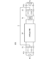
- FIG. 1 is a circuit diagram of a power factor improving switching power supply device 101 according to the first embodiment.
- FIG. 2 is a circuit diagram of a power factor improving switching power supply device 101 showing a specific configuration in the power factor improving circuit 10.
- FIG. 3 is a circuit diagram of the power factor improving switching power supply device 102A according to the second embodiment.
- FIG. 4 is a circuit diagram of another power factor improving switching power supply device 102B according to the second embodiment.
- FIG. 5 is a circuit diagram of the power factor improving switching power supply device 103 according to the third embodiment.
- FIG. 6 is a circuit diagram of the power factor improving switching power supply device 104A according to the fourth embodiment.
- FIG. 7 is a circuit diagram of another power factor improving switching power supply device 104B according to the fourth embodiment.
- FIG. 8 is a circuit diagram of the power factor improving switching power supply devices 105A and 105B according to the fifth embodiment.
- FIG. 9 is a circuit diagram of still another power factor improving switching power supply device 105C, 105D, 105E according to the fifth embodiment.
- FIG. 10 is a circuit diagram of the power factor improving switching power supply device 106A according to the sixth embodiment.
- FIG. 11 is a circuit diagram of another power factor improving switching power supply device 106B according to the sixth embodiment.
- FIG. 12 is a circuit diagram of the power factor improving switching power supply device 107 according to the seventh embodiment.
- FIG. 13 is a circuit diagram of the power factor improving switching power supply device 108 according to the eighth embodiment.
- FIG. 14 is a circuit diagram of the power factor improving switching power supply device 109 according to the ninth embodiment.
- FIG. 1 is a circuit diagram of a power factor improving switching power supply device 101 according to the first embodiment.
- the power factor improving switching power supply device 101 is a circuit connected between the commercial AC power supply AC and the load circuit RL. Further, the power factor improving switching power supply device 101 includes an AC input line ACL and a DC output line DCL. Further, the power factor improving switching power supply device 101 is a circuit 21 composed of a power factor improving circuit 10 and capacitors C11 and C12 connected between the AC input line ACL and connected in series with each other (hereinafter, "first half").
- a circuit 22 (hereinafter referred to as a "second half-bridge capacitor circuit") composed of capacitors C21 and C22 connected between DC output lines DCL and connected in series to each other, and a power factor.
- a common mode choke coil 31 provided between the power factor improving circuit 10 and the second half-bridge capacitor circuit 22 is provided.
- the power factor improving switching power supply device 101 includes an electric path 1 that electrically connects the midpoint of the first half-bridge capacitor circuit 21 and the midpoint of the second half-bridge capacitor circuit 22.
- an electric path 1 that electrically connects the midpoint of the first half-bridge capacitor circuit 21 and the midpoint of 22 of the second half-bridge capacitor circuit by the electric path 1.
- a noise balancing circuit is configured. More specifically, common mode noise has a relatively high frequency and is out of phase. Therefore, these common mode noises cancel each other out by flowing through the electric path 1, and the common mode noises are equilibrated.
- FIG. 2 is a circuit diagram of a power factor improving switching power supply device 101 showing a specific configuration in the power factor improving circuit 10.
- the power factor improving circuit 10 includes inductors L1 and L2 connected in series to the AC input line ACL, a rectifier circuit 11, a first output capacitor Co1 that smoothes the output voltage of the rectifier circuit 11 with a relatively small time constant, and a rectifier.
- An output voltage detection circuit 13 for detecting the output voltage of the circuit 11 and a feedback control circuit 14 are provided.
- the rectifier circuit 11 is composed of diodes D1 and D2 and a switching circuit 12.
- the switching circuit 12 is composed of switch elements Q1 and Q2, and a switching current flows through the inductors L1 and L2 by switching of the switch elements Q1 and Q2.
- the feedback control circuit 14 controls the switching circuit 12 according to the change in voltage between the AC input lines so that the outline of the current waveform flowing through the AC input line ACL follows the outline of the voltage waveform of the AC input line ACL.
- the switching circuit 12 is controlled so that the output voltage of the first output capacitor Co1 becomes a predetermined voltage.
- the electric path 1 is maintained at a potential different from that of the ground or the frame ground, the leakage current does not increase so much, for example, it is suppressed to 1 mA or less, and the risk of electric shock does not increase.
- a power factor-improved switching power supply device can be obtained in which the feedback control is hardly affected even if the capacitance is increased and the increase in leakage current is small. Furthermore, by providing the configuration of the power factor improving switching power supply device 101, the feedback control is hardly affected even if the capacity of the filter capacitor is increased, and the increase in leakage current is small, so that redesigning is not required. The design period can be significantly shortened. Further, by this, it is possible to suppress EMI noise, power integrity (ensuring power supply quality), and shorten the design period of the power factor improving switching power supply device at the same time.
- Second Embodiment a power factor improving switching power supply device including an input capacitor and a power factor improving switching power supply device including a second output capacitor will be exemplified.
- FIG. 3 is a circuit diagram of the power factor improving switching power supply device 102A according to the second embodiment.
- the power factor improving switching power supply device 102A is a circuit connected between the commercial AC power supply AC and the load circuit RL.
- the power factor improving switching power supply device 102A includes an AC input line ACL and a DC output line DCL.
- the power factor improving switching power supply device 102A includes a power factor improving circuit 10, a first half-bridge capacitor circuit 21, a second half-bridge capacitor circuit 22, and a common mode choke coil 31.
- the power factor improving switching power supply device 102A further includes an input capacitor C1 connected in parallel to the first half-bridge capacitor circuit 21.
- FIG. 4 is a circuit diagram of another power factor improving switching power supply device 102B according to the second embodiment.
- the power factor improving switching power supply device 102B is a circuit connected between the commercial AC power supply AC and the load circuit RL.
- the power factor improving switching power supply device 102B includes an AC input line ACL and a DC output line DCL.
- the power factor improving switching power supply device 102B includes a power factor improving circuit 10, a first half-bridge capacitor circuit 21, a second half-bridge capacitor circuit 22, and a common mode choke coil 31.
- the power factor improving switching power supply device 102B includes a second output capacitor Co2 connected in parallel to the second half-bridge capacitor circuit 22.
- FIG. 5 is a circuit diagram of the power factor improving switching power supply device 103 according to the third embodiment.
- the power factor improving switching power supply device 103 is a circuit connected between the commercial AC power supply AC and the load circuit RL.
- the power factor improving switching power supply device 103 includes a power factor improving circuit 10, a first half-bridge capacitor circuit 21, a second half-bridge capacitor circuit 22, a power factor improving circuit 10, and a second half-bridge capacitor circuit 22.
- a common mode choke coil 31 provided between them is provided.
- the power factor improving switching power supply 103 of the present embodiment includes an AC line filter circuit 4 connected between the AC input line ACL and the first half-bridge capacitor circuit 21.
- the AC line filter circuit 4 comprises a line bypass capacitor circuit consisting of capacitors C41, C42, and C43 connected in parallel between AC lines, capacitors C44, and C45 connected between AC lines, and a common mode choke coil 41, 42. Be prepared.
- the midpoint of the line bypass capacitor circuit is grounded to ground or frame ground.
- the EMI noise reduction effect is further improved.
- the common mode noise in the 150 kHz band which is the lower frequency band among the frequency bands from 150 kHz to 30 MHz, is suppressed.
- the self-inductance value of the coils L11 and L12 constituting the common mode choke coil 31 is higher than the highest self-inductance value among the coils L41, L42, L43 and L44 constituting the common mode choke coils 41 and 42 for AC line filters. Is also small.
- the inductance of the coils L41, L42, L43, and L44 is 1 to 3 mH (several mH order), while the inductance of the coils L11 and L12 is 500 ⁇ H (several hundred ⁇ H order). This makes it possible to reduce the size and cost of the equipment.
- FIG. 6 is a circuit diagram of the power factor improving switching power supply device 104A according to the fourth embodiment.
- the power factor improving switching power supply device 104A is a circuit connected between the commercial AC power supply AC and the load circuit RL.
- the power factor improving switching power supply device 104A includes an AC input line ACL and a DC output line DCL.
- the power factor improving switching power supply device 104A includes a power factor improving circuit 10, a first half-bridge capacitor circuit 21, a second half-bridge capacitor circuit 22, and a common mode choke coil 31.
- the common mode choke coil 31 is connected between the power factor improving circuit 10 and the second half bridge capacitor circuit 22.
- the common mode choke coil 31 is connected between the first half bridge capacitor circuit 21 and the power factor improving circuit 10.
- FIG. 7 is a circuit diagram of another power factor improving switching power supply device 104B according to the fourth embodiment.
- the power factor improving switching power supply device 104B is a circuit connected between the commercial AC power supply AC and the load circuit RL.
- the power factor improving switching power supply device 104B includes a power factor improving circuit 10, a first half bridge capacitor circuit 21, a second half bridge capacitor circuit 22, a power factor improving circuit 10, and a common mode choke coil 31. ..
- the common mode choke coil 31 is connected between the power factor improving circuit 10 and the second half bridge capacitor circuit 22.
- the common mode choke coil 31 is connected between the AC line filter circuit 4 and the power factor improving circuit 10.
- the fourth embodiment also has the same effect as the first embodiment.
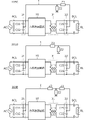
- FIG. 8 is a circuit diagram of the power factor improving switching power supply devices 105A and 105B according to the fifth embodiment.
- These power factor improving switching power supply devices 105A and 105B include a power factor improving circuit 10, a first half bridge capacitor circuit 21, a second half bridge capacitor circuit 22, and a common mode choke coil 31. Further, an electric path 1 for electrically connecting the midpoint of the first half-bridge capacitor circuit 21 and the midpoint of the second half-bridge capacitor circuit 22 is provided.
- the impedance element Z1 is connected in series to the electric path 1 of the power factor improving switching power supply device 105A.
- This impedance element Z1 has at least an inductance component or a resistance component.
- An impedance element Z2 is connected between the electric path 1 of the power factor improving switching power supply device 105B and the ground.
- the impedance element Z2 has at least a capacitance component, an inductance component, or a resistance component.
- This "ground” is a ground or a frame ground.
- the impedance element Z1 By connecting the impedance element Z1 in series to the electric path 1 as in the power factor improving switching power supply device 105A, even if the effect of suppressing the common mode noise by the common mode choke coil 31 is insufficient, the impedance element Z1 can be used. The suppression of common mode noise is supplemented. That is, the impedance element Z1 consumes the energy that the first half-bridge capacitor circuit 21 and the second half-bridge capacitor circuit 22 move to balance through the electric path 1 as heat, so that the common mode noise is suppressed accordingly. ..
- the impedance element Z2 is connected between the electric path 1 and the ground.
- the impedance element Z2 has at least a capacitance component, an inductance component, or a resistance component.
- the impedance element Z2 By connecting the impedance element Z2 between the electric path 1 and the ground in this way, even if the effect of suppressing the common mode noise by the common mode choke coil 31 is insufficient, the impedance element Z2 causes the common mode noise. Suppression is supplemented. That is, the current that flows for the first half-bridge capacitor circuit 21 and the second half-bridge capacitor circuit 22 to balance through the electric path 1 flows to the ground through the impedance element Z2. This current (leakage current) is smaller than the current leaking from the line bypass capacitor circuit to the ground when the line bypass capacitor circuit is provided. Therefore, the leakage current does not increase, and the influence on the feedback circuit can be further reduced.
- FIG. 9 is a circuit diagram of yet another power factor improving switching power supply device 105C, 105D, 105E according to the fifth embodiment.
- the impedance element Z2 is connected between the electric path 1 and the ground.
- the impedance element Z1 is connected in series between the connection point of the impedance element Z2 with respect to the electric path 1 and the middle point of the second half bridge capacitor circuit 22. Further, in the power factor improving switching power supply device 105D, the impedance element Z3 is connected in series between the connection point of the impedance element Z2 with respect to the electric path 1 and the middle point of the first half-bridge capacitor circuit 21. In the power factor improving switching power supply device 105E, the impedance element Z1 is connected in series between the connection point of the impedance element Z2 with respect to the electric path 1 and the midpoint of the second half bridge capacitor circuit 22, and the impedance with respect to the electric path 1 is provided. The impedance element Z3 is connected in series between the connection point of the element Z2 and the middle point of the first half-bridge capacitor circuit 21.
- each power factor improving switching power supply device 105C, 105D, 105E shown in FIG. 9 if the impedance elements Z1 and Z3 are resistors or inductors and the impedance element Z2 is a capacitor, the low-pass filter is configured by these impedance elements. .. If the impedance elements Z1 and Z3 are capacitors and the impedance elements Z2 are resistors or inductors, these impedance elements constitute a high-pass filter.
- ⁇ 6th Embodiment a power factor improving switching power supply device in which the configurations of the rectifier circuit 11 and the switching circuit 12 are different from the examples shown so far is shown.
- FIG. 10 is a circuit diagram of the power factor improving switching power supply device 106A according to the sixth embodiment.
- the power factor improving circuit 10 of the power factor improving switching power supply device 106A includes inductors L1 and L2 connected in series to the AC input line ACL, a rectifier circuit 11, and a first output capacitor Co1 that smoothes the output voltage of the rectifier circuit 11.
- the output voltage detection circuit 13 for detecting the output voltage of the rectifier circuit 11 and the feedback control circuit 14 are provided.
- the rectifier circuit 11 is composed of diodes D1 and D2 and a switching circuit 12.
- the switching circuit 12 is composed of switch elements Q1 and Q3, and a switching current flows through the inductors L1 and L2 by switching of the switch elements Q1 and Q3.
- Other configurations are the same as the configuration of the circuit shown in FIG. 2 in the first embodiment. In this way, switch elements may be provided on the high side and the low side.
- FIG. 11 is a circuit diagram of another power factor improving switching power supply device 106B according to the sixth embodiment.
- the rectifier circuit 11 of the power factor improving circuit 10 of the power factor improving switching power supply device 106B is composed of switch elements Q1, Q2, Q3, and Q4. By switching these switch elements Q1, Q2, Q3, and Q4, a switching current flows through the inductors L1 and L2.
- Other configurations are the same as the configuration of the circuit shown in FIG. 2 in the first embodiment. In this way, a switching circuit and a rectifier circuit having a bridge circuit configuration may be configured with four switch elements.
- FIG. 12 is a circuit diagram of the power factor improving switching power supply device 107 according to the seventh embodiment.
- the power factor improving circuit 10 detects the inductor L1 connected in series to the AC input line ACL, the rectifier circuit 11, the first output capacitor Co1 that smoothes the output voltage of the rectifier circuit 11, and the output voltage of the rectifier circuit 11. It includes an output voltage detection circuit 13 and a feedback control circuit 14.
- the inductor L1 is connected to only one line of the AC input line ACL.
- Other configurations are as shown in the first embodiment.
- the inductor in which the switching current flows by the switching circuit may be provided only in one line of the AC input line ACL.
- FIG. 13 is a circuit diagram of the power factor improving switching power supply device 108 according to the eighth embodiment.
- the power factor improving circuit 10 includes inductors L1A and L1B connected in series to the AC input line ACL, a rectifier circuit 11, a first output capacitor Co1 that smoothes the output voltage of the rectifier circuit 11 with a relatively small time constant, and a rectifier.
- An output voltage detection circuit 13 for detecting the output voltage of the circuit 11 and a feedback control circuit 14 are provided.
- the rectifier circuit 11 is composed of diodes D1, D2, D3 and a switching circuit 12.
- the switching circuit 12 is composed of switch elements Q1, Q2, and Q3.
- the diode D1 and the switch element Q1 are connected in series, and one end of the inductor L1A is connected to the connection point.
- the diode D3 and the switch element Q3 are connected in series, and one end of the inductor L1B is connected to the connection point.
- the diode D2 and the switch element Q2 are connected in series, and the connection point thereof is connected to the AC input line ACL on the side to which the inductors L1A and L1B are not connected.
- the feedback control circuit 14 alternately turns on the switch element Q1 and the switch element Q2, and turns on the switch element Q3 and the switch element Q2. In this way, the rectifier circuit 11 that operates in an interleaved manner may be provided.
- FIG. 14 is a circuit diagram of the power factor improving switching power supply device 109 according to the ninth embodiment.
- the power factor improving switching power supply device 109 is a circuit connected between the commercial AC power supply AC and the load circuit RL. Further, the power factor improving switching power supply device 109 is connected between the first half-bridge capacitor circuit 21 which is connected between the AC input lines ACL and is composed of two capacitors connected in series with each other, and is connected between the DC output line DCL.
- a second half-bridge capacitor circuit 22 composed of two capacitors connected in series to each other, a power factor improving circuit 10, a common mode choke coil 31, and a diode bridge circuit DB are provided.
- the diode bridge circuit DB full-wave rectifies the AC voltage of the AC input line ACL.
- the power factor improving circuit 10 includes an output voltage detection circuit 13, a first output capacitor Co1, an inductor L5, a switch element Q5, a diode D5, and a capacitor C5.
- a step-up chopper circuit is composed of an inductor L5, a switch element Q5, a diode D5, and a capacitor C5.
- the switch element Q5 constitutes a switching circuit 12.
- the feedback control circuit 14 controls the switching circuit 12 according to the change in voltage between the AC input lines so that the outline of the current waveform flowing through the AC input line ACL follows the outline of the voltage waveform of the AC input line ACL.
- the switching circuit 12 is controlled so that the output voltage of the first output capacitor Co1 becomes a predetermined voltage.
- the present invention can also be applied to a circuit provided with a diode bridge circuit DB between the AC input line ACL and the switching circuit 12.
- AC ... Commercial AC power supply ACL ... AC input line C1 ... Input capacitors C11, C12, C21, C22 ... Capacitors C41, C42, C43, C44, C45 ... Condenser C5 ... Capacitor Co1 ... First output capacitor Co2 ... Second output capacitor D1 , D2, D3, D5 ... Diode DB ... Diode bridge circuit DCL ... DC output line L1, L2 ... Inductor L11, L12 ... Coil L1A, L1B ... Inverter L41, L42, L43, L44 ... Coil L5 ... Capacitor Q1, Q2, Q3 , Q4, Q5 ... Switch element RL ...
Landscapes
- Engineering & Computer Science (AREA)
- Power Engineering (AREA)
- Physics & Mathematics (AREA)
- Electromagnetism (AREA)
- Rectifiers (AREA)
- Dc-Dc Converters (AREA)
Priority Applications (2)
| Application Number | Priority Date | Filing Date | Title |
|---|---|---|---|
| JP2022572130A JP7400995B2 (ja) | 2020-12-21 | 2021-12-10 | 力率改善スイッチング電源装置 |
| US18/334,154 US12431793B2 (en) | 2020-12-21 | 2023-06-13 | Power factor correction switching power supply device |
Applications Claiming Priority (2)
| Application Number | Priority Date | Filing Date | Title |
|---|---|---|---|
| JP2020-210979 | 2020-12-21 | ||
| JP2020210979 | 2020-12-21 |
Related Child Applications (1)
| Application Number | Title | Priority Date | Filing Date |
|---|---|---|---|
| US18/334,154 Continuation US12431793B2 (en) | 2020-12-21 | 2023-06-13 | Power factor correction switching power supply device |
Publications (1)
| Publication Number | Publication Date |
|---|---|
| WO2022138217A1 true WO2022138217A1 (ja) | 2022-06-30 |
Family
ID=82159703
Family Applications (1)
| Application Number | Title | Priority Date | Filing Date |
|---|---|---|---|
| PCT/JP2021/045426 Ceased WO2022138217A1 (ja) | 2020-12-21 | 2021-12-10 | 力率改善スイッチング電源装置 |
Country Status (3)
| Country | Link |
|---|---|
| US (1) | US12431793B2 (https=) |
| JP (1) | JP7400995B2 (https=) |
| WO (1) | WO2022138217A1 (https=) |
Cited By (1)
| Publication number | Priority date | Publication date | Assignee | Title |
|---|---|---|---|---|
| WO2024179349A1 (zh) * | 2023-03-02 | 2024-09-06 | 广东美的制冷设备有限公司 | Pfc电路及其控制方法、电器设备、存储介质 |
Citations (4)
| Publication number | Priority date | Publication date | Assignee | Title |
|---|---|---|---|---|
| JP2009095183A (ja) * | 2007-10-11 | 2009-04-30 | Eta Electric Industry Co Ltd | スイッチング電源装置 |
| JP2016058495A (ja) * | 2014-09-08 | 2016-04-21 | 株式会社東芝 | コモンモードチョークコイル、コモンモードフィルタ、および電力変換装置 |
| JP2018161024A (ja) * | 2017-03-21 | 2018-10-11 | 株式会社東芝 | 電力変換装置及び電力変換システム |
| JP2019205317A (ja) * | 2018-05-25 | 2019-11-28 | 株式会社豊田自動織機 | 車載用電力変換装置 |
Family Cites Families (10)
| Publication number | Priority date | Publication date | Assignee | Title |
|---|---|---|---|---|
| JP2005033895A (ja) * | 2003-07-10 | 2005-02-03 | Toshiba Corp | 電力変換装置 |
| US7215560B2 (en) | 2004-12-14 | 2007-05-08 | International Rectifier Corporation | EMI noise reduction circuit and method for bridgeless PFC circuit |
| JP6191542B2 (ja) | 2014-05-21 | 2017-09-06 | 株式会社デンソー | 電力変換装置 |
| JP2016158316A (ja) | 2015-02-23 | 2016-09-01 | 株式会社豊田自動織機 | 電源装置 |
| JP6260578B2 (ja) * | 2015-04-17 | 2018-01-17 | トヨタ自動車株式会社 | 送電装置及び受電装置 |
| WO2019130874A1 (ja) * | 2017-12-27 | 2019-07-04 | 株式会社村田製作所 | 電源装置 |
| JP7087887B2 (ja) * | 2018-09-27 | 2022-06-21 | Tdk株式会社 | スイッチング電源装置 |
| US11601042B2 (en) * | 2020-05-14 | 2023-03-07 | Delta Electronics, Inc. | Multi-phase AC/DC converter |
| JPWO2021230137A1 (https=) * | 2020-05-15 | 2021-11-18 | ||
| US11211872B1 (en) * | 2020-09-28 | 2021-12-28 | Delta Electronics, Inc. | Power-factor-correction rectifiers with soft switching |
-
2021
- 2021-12-10 WO PCT/JP2021/045426 patent/WO2022138217A1/ja not_active Ceased
- 2021-12-10 JP JP2022572130A patent/JP7400995B2/ja active Active
-
2023
- 2023-06-13 US US18/334,154 patent/US12431793B2/en active Active
Patent Citations (4)
| Publication number | Priority date | Publication date | Assignee | Title |
|---|---|---|---|---|
| JP2009095183A (ja) * | 2007-10-11 | 2009-04-30 | Eta Electric Industry Co Ltd | スイッチング電源装置 |
| JP2016058495A (ja) * | 2014-09-08 | 2016-04-21 | 株式会社東芝 | コモンモードチョークコイル、コモンモードフィルタ、および電力変換装置 |
| JP2018161024A (ja) * | 2017-03-21 | 2018-10-11 | 株式会社東芝 | 電力変換装置及び電力変換システム |
| JP2019205317A (ja) * | 2018-05-25 | 2019-11-28 | 株式会社豊田自動織機 | 車載用電力変換装置 |
Cited By (1)
| Publication number | Priority date | Publication date | Assignee | Title |
|---|---|---|---|---|
| WO2024179349A1 (zh) * | 2023-03-02 | 2024-09-06 | 广东美的制冷设备有限公司 | Pfc电路及其控制方法、电器设备、存储介质 |
Also Published As
| Publication number | Publication date |
|---|---|
| US20230327545A1 (en) | 2023-10-12 |
| JP7400995B2 (ja) | 2023-12-19 |
| US12431793B2 (en) | 2025-09-30 |
| JPWO2022138217A1 (https=) | 2022-06-30 |
Similar Documents
| Publication | Publication Date | Title |
|---|---|---|
| US7898827B2 (en) | Active EMI filtering using magnetic coupling cancellation | |
| US5777866A (en) | Power factor control for switched mode rectifiers with improved representing of currents in EMI capacitive elements | |
| JP7252376B2 (ja) | 電圧又は電流を補償する装置 | |
| KR20030002685A (ko) | 전도성 전자기 장애 제거를 위한 능동형 커먼모드이엠아이 필터 | |
| CN100423430C (zh) | 宽带宽ac-dc功率转换器 | |
| JP7012232B2 (ja) | 電源回路 | |
| Kong et al. | Common mode EMI noise characteristics of low-power AC–DC converters | |
| JP7400995B2 (ja) | 力率改善スイッチング電源装置 | |
| JP5030157B2 (ja) | スイッチング電源装置 | |
| WO2022048287A1 (zh) | 一种dc/dc变换器及通信电源 | |
| Chen et al. | Common-mode noise reduction with impedance balancing in DC-fed motor drives | |
| JP7563487B2 (ja) | スイッチング電源装置 | |
| JPH10256859A (ja) | Acラインフィルタ | |
| JP7597127B2 (ja) | スイッチング電源装置 | |
| JP7029701B2 (ja) | 電源回路 | |
| JP2009148045A (ja) | 漏洩電流低減装置 | |
| CA3011542C (en) | Filters for adjustable speed drives with low dc bus capacitance and methods of manufacture and use thereof | |
| CN115051552A (zh) | 抑制pfc变换器共模传导干扰的电路及空调器 | |
| JPWO2022138217A5 (https=) | ||
| JP7012231B2 (ja) | 電源回路 | |
| JPH1075565A (ja) | 電子機器用高調波電流抑制装置 | |
| Anwar et al. | Design and Analysis of Differential Mode Active EMI Filter for GaN-based Totem Pole PFC Converter | |
| CN121150493A (zh) | 谐振转换器 | |
| JP2026061070A (ja) | ノイズ低減装置および空気調和装置 | |
| Bijeev et al. | A study of input filter design for high power high frequency space applications |
Legal Events
| Date | Code | Title | Description |
|---|---|---|---|
| 121 | Ep: the epo has been informed by wipo that ep was designated in this application |
Ref document number: 21910366 Country of ref document: EP Kind code of ref document: A1 |
|
| ENP | Entry into the national phase |
Ref document number: 2022572130 Country of ref document: JP Kind code of ref document: A |
|
| NENP | Non-entry into the national phase |
Ref country code: DE |
|
| 122 | Ep: pct application non-entry in european phase |
Ref document number: 21910366 Country of ref document: EP Kind code of ref document: A1 |