WO2022124281A1 - 制御装置、調整方法、リソグラフィ装置、及び物品の製造方法 - Google Patents
制御装置、調整方法、リソグラフィ装置、及び物品の製造方法 Download PDFInfo
- Publication number
- WO2022124281A1 WO2022124281A1 PCT/JP2021/044806 JP2021044806W WO2022124281A1 WO 2022124281 A1 WO2022124281 A1 WO 2022124281A1 JP 2021044806 W JP2021044806 W JP 2021044806W WO 2022124281 A1 WO2022124281 A1 WO 2022124281A1
- Authority
- WO
- WIPO (PCT)
- Prior art keywords
- control
- signal
- control device
- adjustment
- deviation
- Prior art date
Links
- 238000004519 manufacturing process Methods 0.000 title claims description 40
- 238000000034 method Methods 0.000 title claims description 36
- 238000001459 lithography Methods 0.000 title claims description 7
- 238000013528 artificial neural network Methods 0.000 claims abstract description 41
- 238000012937 correction Methods 0.000 claims abstract description 19
- 238000004364 calculation method Methods 0.000 claims abstract description 9
- 230000014509 gene expression Effects 0.000 claims description 18
- 239000000758 substrate Substances 0.000 claims description 14
- 238000012545 processing Methods 0.000 claims description 8
- 238000012546 transfer Methods 0.000 claims description 6
- 230000004069 differentiation Effects 0.000 claims description 3
- 238000010801 machine learning Methods 0.000 claims description 3
- 230000008569 process Effects 0.000 description 22
- 230000008859 change Effects 0.000 description 13
- 230000001629 suppression Effects 0.000 description 13
- 238000012790 confirmation Methods 0.000 description 9
- 238000010586 diagram Methods 0.000 description 9
- 230000003287 optical effect Effects 0.000 description 6
- 238000004458 analytical method Methods 0.000 description 5
- 238000005286 illumination Methods 0.000 description 5
- 239000000463 material Substances 0.000 description 5
- 230000001360 synchronised effect Effects 0.000 description 5
- 238000005259 measurement Methods 0.000 description 4
- 238000001228 spectrum Methods 0.000 description 4
- 230000006870 function Effects 0.000 description 3
- 230000000694 effects Effects 0.000 description 2
- 230000010354 integration Effects 0.000 description 2
- 238000012986 modification Methods 0.000 description 2
- 230000004048 modification Effects 0.000 description 2
- 230000004044 response Effects 0.000 description 2
- 238000002945 steepest descent method Methods 0.000 description 2
- 230000001133 acceleration Effects 0.000 description 1
- 230000015572 biosynthetic process Effects 0.000 description 1
- 239000003795 chemical substances by application Substances 0.000 description 1
- 238000007796 conventional method Methods 0.000 description 1
- 238000010894 electron beam technology Methods 0.000 description 1
- 238000005530 etching Methods 0.000 description 1
- 238000010438 heat treatment Methods 0.000 description 1
- QSHDDOUJBYECFT-UHFFFAOYSA-N mercury Chemical compound [Hg] QSHDDOUJBYECFT-UHFFFAOYSA-N 0.000 description 1
- 229910052753 mercury Inorganic materials 0.000 description 1
- 230000003647 oxidation Effects 0.000 description 1
- 238000007254 oxidation reaction Methods 0.000 description 1
- 238000004806 packaging method and process Methods 0.000 description 1
- 238000000206 photolithography Methods 0.000 description 1
- 230000009467 reduction Effects 0.000 description 1
- 230000002787 reinforcement Effects 0.000 description 1
- 239000004065 semiconductor Substances 0.000 description 1
- 238000012360 testing method Methods 0.000 description 1
- 230000007723 transport mechanism Effects 0.000 description 1
- 238000007740 vapor deposition Methods 0.000 description 1
Images


Classifications
-
- G—PHYSICS
- G05—CONTROLLING; REGULATING
- G05B—CONTROL OR REGULATING SYSTEMS IN GENERAL; FUNCTIONAL ELEMENTS OF SUCH SYSTEMS; MONITORING OR TESTING ARRANGEMENTS FOR SUCH SYSTEMS OR ELEMENTS
- G05B11/00—Automatic controllers
- G05B11/01—Automatic controllers electric
- G05B11/36—Automatic controllers electric with provision for obtaining particular characteristics, e.g. proportional, integral, differential
-
- G—PHYSICS
- G03—PHOTOGRAPHY; CINEMATOGRAPHY; ANALOGOUS TECHNIQUES USING WAVES OTHER THAN OPTICAL WAVES; ELECTROGRAPHY; HOLOGRAPHY
- G03F—PHOTOMECHANICAL PRODUCTION OF TEXTURED OR PATTERNED SURFACES, e.g. FOR PRINTING, FOR PROCESSING OF SEMICONDUCTOR DEVICES; MATERIALS THEREFOR; ORIGINALS THEREFOR; APPARATUS SPECIALLY ADAPTED THEREFOR
- G03F7/00—Photomechanical, e.g. photolithographic, production of textured or patterned surfaces, e.g. printing surfaces; Materials therefor, e.g. comprising photoresists; Apparatus specially adapted therefor
- G03F7/20—Exposure; Apparatus therefor
-
- G—PHYSICS
- G03—PHOTOGRAPHY; CINEMATOGRAPHY; ANALOGOUS TECHNIQUES USING WAVES OTHER THAN OPTICAL WAVES; ELECTROGRAPHY; HOLOGRAPHY
- G03F—PHOTOMECHANICAL PRODUCTION OF TEXTURED OR PATTERNED SURFACES, e.g. FOR PRINTING, FOR PROCESSING OF SEMICONDUCTOR DEVICES; MATERIALS THEREFOR; ORIGINALS THEREFOR; APPARATUS SPECIALLY ADAPTED THEREFOR
- G03F7/00—Photomechanical, e.g. photolithographic, production of textured or patterned surfaces, e.g. printing surfaces; Materials therefor, e.g. comprising photoresists; Apparatus specially adapted therefor
- G03F7/70—Microphotolithographic exposure; Apparatus therefor
- G03F7/70691—Handling of masks or workpieces
- G03F7/70775—Position control, e.g. interferometers or encoders for determining the stage position
-
- G—PHYSICS
- G05—CONTROLLING; REGULATING
- G05B—CONTROL OR REGULATING SYSTEMS IN GENERAL; FUNCTIONAL ELEMENTS OF SUCH SYSTEMS; MONITORING OR TESTING ARRANGEMENTS FOR SUCH SYSTEMS OR ELEMENTS
- G05B13/00—Adaptive control systems, i.e. systems automatically adjusting themselves to have a performance which is optimum according to some preassigned criterion
- G05B13/02—Adaptive control systems, i.e. systems automatically adjusting themselves to have a performance which is optimum according to some preassigned criterion electric
- G05B13/0265—Adaptive control systems, i.e. systems automatically adjusting themselves to have a performance which is optimum according to some preassigned criterion electric the criterion being a learning criterion
- G05B13/027—Adaptive control systems, i.e. systems automatically adjusting themselves to have a performance which is optimum according to some preassigned criterion electric the criterion being a learning criterion using neural networks only
-
- H—ELECTRICITY
- H01—ELECTRIC ELEMENTS
- H01L—SEMICONDUCTOR DEVICES NOT COVERED BY CLASS H10
- H01L21/00—Processes or apparatus adapted for the manufacture or treatment of semiconductor or solid state devices or of parts thereof
- H01L21/02—Manufacture or treatment of semiconductor devices or of parts thereof
- H01L21/027—Making masks on semiconductor bodies for further photolithographic processing not provided for in group H01L21/18 or H01L21/34
-
- H—ELECTRICITY
- H01—ELECTRIC ELEMENTS
- H01L—SEMICONDUCTOR DEVICES NOT COVERED BY CLASS H10
- H01L21/00—Processes or apparatus adapted for the manufacture or treatment of semiconductor or solid state devices or of parts thereof
- H01L21/67—Apparatus specially adapted for handling semiconductor or electric solid state devices during manufacture or treatment thereof; Apparatus specially adapted for handling wafers during manufacture or treatment of semiconductor or electric solid state devices or components ; Apparatus not specifically provided for elsewhere
- H01L21/68—Apparatus specially adapted for handling semiconductor or electric solid state devices during manufacture or treatment thereof; Apparatus specially adapted for handling wafers during manufacture or treatment of semiconductor or electric solid state devices or components ; Apparatus not specifically provided for elsewhere for positioning, orientation or alignment
Landscapes
- Engineering & Computer Science (AREA)
- General Physics & Mathematics (AREA)
- Physics & Mathematics (AREA)
- Artificial Intelligence (AREA)
- Condensed Matter Physics & Semiconductors (AREA)
- Manufacturing & Machinery (AREA)
- Computer Hardware Design (AREA)
- Microelectronics & Electronic Packaging (AREA)
- Power Engineering (AREA)
- Automation & Control Theory (AREA)
- Evolutionary Computation (AREA)
- Health & Medical Sciences (AREA)
- Computer Vision & Pattern Recognition (AREA)
- Medical Informatics (AREA)
- Software Systems (AREA)
- Feedback Control In General (AREA)
- Exposure And Positioning Against Photoresist Photosensitive Materials (AREA)
- Container, Conveyance, Adherence, Positioning, Of Wafer (AREA)
- Exposure Of Semiconductors, Excluding Electron Or Ion Beam Exposure (AREA)
Abstract
Description
図1には、本実施形態におけるシステムSSの構成が示されている。システムSSは、例えば、物品を製造するための製造装置に適用される。製造装置は、例えば、物品、または物品の一部を構成する部材を処理する処理装置を含む。処理装置は、例えば、材料または部材にパターンを転写するリソグラフィ装置、材料または部材に膜を形成する膜形成装置、材料または部材をエッチングする装置、および、材料または部材を加熱する加熱装置のいずれかでありうる。
実施例1において、第1調整部303a、第2調整部303bは、以下の式(1)で表される制御特性を有する。ここで、補正器303に対する入力(E)をx、補正器303の出力(CS)をy、任意の係数(定数)をKpとする。
実施例2において、第1調整部303a、第2調整部303bは、以下の式(2)で表される制御特性を有する。ここで、補正器303に対する入力(E)をx、補正器303の出力(CS)をy、時刻をt、任意の係数(定数)をKiとする。なお、積分は複数回行ってもよい。積分はある時間区間の定積分でもよいし、不定積分でもよい。

実施例3において、第1調整部303a、第2調整部303bは、以下の式(3)で表される制御特性を有する。ここで、補正器303に対する入力(E)をx、補正器303の出力(CS)をy、時刻をt、任意の係数(定数)Kdとする。なお、微分は複数回行ってもよい。

実施例4において、第1調整部303a、第2調整部303bは、以下の式(4)で表される制御特性を有する。ここで、補正器303に対する入力(E)をx、補正器303の出力(CS)をy、任意の係数(定数)をKp、Ki、Kdとする。なお、積分および微分は複数回行ってもよい。

実施例5において、第1調整部303a、第2調整部303bは、以下の式(5)の演算式で表される制御特性を有する。ここで、補正器303に対する入力(E)をx、補正器303の出力(CS)をy、多重積分の積分階数をn、微分階数をm、任意の係数(定数)をKp、n重積分のときの任意の係数(定数)をKi_n、m階微分のときの任意の定数をKd_mとする。

実施例6~8は、制御状態の変化と、補正器303で用いられる調整部の切り替えの関係性について説明する。
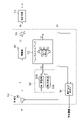
図5は、実施例7における制御器102の構成例を示す図である。実施例7では、制御対象103の状態や動作に応じて補償器301の切り替えを行う構成となっており、補償器301aを使用するか、補償器301bを使用するかを選択できる。実施例7における制御状態とは、複数の補償器のうちどの補償器を使用するかによって定まる状態であり、補償器301aを使用するか、補償器301bを使用するかによって調整部の切り替えを実行する。また、実施例7では、補償器301の状態によって補正器303の切り替えを行う構成となっており、第1調整部303aを使用するか、第2調整部303bを使用するかを選択できる。
図6は、実施例8における制御器102の構成例を示す図である。実施例8における制御状態とは、制御対象の動作パターン403が変化しているか否かによって定まる状態である。動作パターン403の具体例については、後述する。実施例8では、動作パターン403の状態に応じて調整部の切り替えを行う構成となっており、第1調整部303aを使用するか、第2調整部303bを使用するかを選択できる。
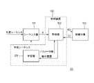
本実施形態では、第1実施形態で説明した制御システムSSをステージ制御装置800に適用する例について説明する。本実施形態として言及しない事項は、第1実施形態に従う。図10は、図1で示した制御システムSSをステージ制御装置800に適用したときのハードウェア構成を示す図である。


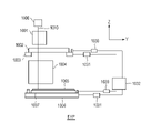
本実施形態では、第1実施形態で説明した制御システムSSを露光装置EXPに適用する例について説明する。本実施形態として言及しない事項は、第1実施形態に従う。図15には、本実施形態の露光装置EXPの構成例が模式的に示されている。露光装置EXPは、走査露光装置として構成されうる。
本発明の実施形態にかかる物品の製造方法は、例えば、フラットパネルディスプレイ(FPD)を製造するのに好適である。本実施形態の物品の製造方法は、基板上に塗布された感光剤に上記の露光装置を用いて潜像パターンを形成する工程(基板を露光する工程)と、かかる工程で潜像パターンが形成された基板を現像する工程とを含む。更に、かかる製造方法は、他の周知の工程(酸化、成膜、蒸着、ドーピング、平坦化、エッチング、レジスト剥離、ダイシング、ボンディング、パッケージング等)を含む。本実施形態の物品の製造方法は、従来の方法に比べて、物品の性能・品質・生産性・生産コストの少なくとも1つにおいて有利である。
Claims (23)
- 制御対象を制御するための制御信号を発生する制御装置であって、
前記制御対象の制御偏差に基づいて第1信号を発生させる第1補償器と、
係数を調整可能な演算式に従って前記制御偏差を補正することによって補正信号を発生させる複数の調整部のうち、1つの調整部を用いて前記制御偏差を補正する補正器と、
前記補正信号に基づいて、ニューラルネットワークにより第2信号を発生する第2補償器と、
前記第1信号と前記第2信号とに基づいて前記制御信号を発生する演算器と、
を備えることを特徴とする制御装置。 - 前記補正器において、前記制御対象の制御状態に基づいて前記複数の調整部から前記制御偏差の補正に用いる調整部が選択されることを特徴とする請求項1に記載の制御装置。
- 前記制御対象と、前記制御対象とは別の制御対象とを同期させて制御するか否かに基づいて前記複数の調整部から前記制御偏差の補正に用いる調整部が選択されることを特徴とする請求項1又は2に記載の制御装置。
- 前記制御対象のゲインの切り替えが生じているか否かに基づいて前記複数の調整部から前記制御偏差の補正に用いる調整部が選択されることを特徴とする請求項1又は2に記載の制御装置。
- 前記第1補償器の状態に基づいて前記複数の調整部から前記制御偏差の補正に用いる調整部が選択されることを特徴とする請求項1又は2に記載の制御装置。
- 前記制御対象の動作パターンが変化しているか否かに基づいて前記複数の調整部から前記制御偏差の補正に用いる調整部が選択されることを特徴とする請求項1又は2に記載の制御装置。
- 前記演算式は、前記制御偏差に比例する項を含むことを特徴とする請求項1乃至6のいずれか1項に記載の制御装置。
- 前記演算式は、前記制御偏差に積分を行う項を含むことを特徴とする請求項1乃至7のいずれか1項に記載の制御装置。
- 前記演算式は、前記制御偏差に微分を行う項を含むことを特徴とする請求項1乃至8のいずれか1項に記載の制御装置。
- 前記演算式は、前記制御偏差に比例する項、積分を行う項、および、微分を行う項、の少なくとも1つを含むことを特徴とする請求項1乃至6のいずれか1項に記載の制御装置。
- 前記補正器を調整する設定部を更に備え、
前記設定部は、前記複数の調整部から前記制御偏差の補正に用いる調整部を選択することを特徴とする請求項1乃至10のいずれか1項に記載の制御装置。 - 前記設定部は、前記演算式を設定することを特徴とする請求項11に記載の制御装置。
- 前記設定部は、前記制御偏差が所定条件を満たす場合に、前記演算式の前記係数を再設定することを特徴とする請求項11又は12に記載の制御装置。
- 前記所定条件は、前記制御偏差が規定値を超えることを含むことを特徴とする請求項13に記載の制御装置。
- 前記ニューラルネットワークのパラメータ値を機械学習によって決定する学習部を更に備えることを特徴とする請求項1乃至14のいずれか1項に記載の制御装置。
- 前記制御信号は、前記第1信号を前記第2信号に基づいて補正した信号であり、
前記第1信号に基づいて前記制御対象を制御した結果である制御量と制御対象を制御するための目標値との差に比べて、前記制御信号に基づいて前記制御対象を制御した結果である制御量と制御対象を制御するための目標値との差の方が小さいことを特徴とする請求項1乃至15のいずれか1項に記載の制御装置。 - 制御対象を制御するための制御信号を発生する制御装置であって、
前記制御対象の制御偏差に基づいて第1信号を発生させる第1補償器と、
演算式に従って前記制御偏差を補正することによって補正信号を発生させる複数の調整部のうち、1つの調整部を用いて前記制御偏差を補正する補正器と、
前記補正信号に基づいて、ニューラルネットワークにより第2信号を発生する第2補償器と、
前記第1信号と前記第2信号とに基づいて前記制御信号を発生する演算器と、
を備えることを特徴とする制御装置。 - 前記補正器において、前記制御対象の制御状態に基づいて前記複数の調整部から前記制御偏差の補正に用いる調整部を選択することを特徴とする請求項17に記載の制御装置。
- 前記演算式は、前記制御偏差に比例する項、積分を行う項、および、微分を行う項、の少なくとも1つを含むことを特徴とする請求項17又は18に記載の制御装置。
- 物体の位置を制御するために、前記物体を保持するステージを制御するステージ制御装置であって、
請求項1乃至19のいずれか1項に記載の制御装置を備えることを特徴とするステージ制御装置。 - 基板に原版のパターンを転写するリソグラフィ装置であって、
前記基板または前記原版の位置を制御するように構成された請求項1乃至19のいずれか1項に記載の制御装置を備えることを特徴とするリソグラフィ装置。 - 請求項21に記載のリソグラフィ装置を用いて基板に原版のパターンを転写する転写工程と、
前記転写工程を経た前記基板を処理する処理工程と、を含み、
前記処理工程を経た前記基板から物品を得ることを特徴とする物品の製造方法。 - 制御対象の制御偏差に基づいて第1信号を発生させる第1補償器と、前記制御偏差を補正することによって補正信号を発生させる複数の調整部のうち、1つの調整部を用いて前記制御偏差を補正する補正器と、前記補正信号に基づいて、ニューラルネットワークにより第2信号を発生する第2補償器と、前記第1信号と前記第2信号とに基づいて制御信号を発生する演算器とを備える制御装置を調整する調整方法であって、
前記補正器において、前記制御対象の制御状態に基づいて前記複数の調整部から前記制御偏差の補正に用いる調整部を選択する調整工程を含む、
ことを特徴とする調整方法。
Priority Applications (2)
| Application Number | Priority Date | Filing Date | Title |
|---|---|---|---|
| KR1020237022519A KR20230118130A (ko) | 2020-12-11 | 2021-12-07 | 제어 장치, 조정 방법, 리소그래피 장치 및 물품의제조 방법 |
| CN202180082084.6A CN116648773A (zh) | 2020-12-11 | 2021-12-07 | 控制装置、调节方法、光刻装置和物品制造方法 |
Applications Claiming Priority (2)
| Application Number | Priority Date | Filing Date | Title |
|---|---|---|---|
| JP2020205546A JP2022092690A (ja) | 2020-12-11 | 2020-12-11 | 制御装置、調整方法、リソグラフィ装置、及び物品の製造方法 |
| JP2020-205546 | 2020-12-11 |
Publications (1)
| Publication Number | Publication Date |
|---|---|
| WO2022124281A1 true WO2022124281A1 (ja) | 2022-06-16 |
Family
ID=81974410
Family Applications (1)
| Application Number | Title | Priority Date | Filing Date |
|---|---|---|---|
| PCT/JP2021/044806 WO2022124281A1 (ja) | 2020-12-11 | 2021-12-07 | 制御装置、調整方法、リソグラフィ装置、及び物品の製造方法 |
Country Status (5)
| Country | Link |
|---|---|
| JP (1) | JP2022092690A (ja) |
| KR (1) | KR20230118130A (ja) |
| CN (1) | CN116648773A (ja) |
| TW (1) | TW202223562A (ja) |
| WO (1) | WO2022124281A1 (ja) |
Cited By (1)
| Publication number | Priority date | Publication date | Assignee | Title |
|---|---|---|---|---|
| WO2024090126A1 (ja) * | 2022-10-25 | 2024-05-02 | キヤノン株式会社 | 制御方法、制御装置、リソグラフィ装置、および物品製造方法 |
Citations (5)
| Publication number | Priority date | Publication date | Assignee | Title |
|---|---|---|---|---|
| JPH03233702A (ja) * | 1990-02-09 | 1991-10-17 | Hitachi Ltd | コントローラの調整方法および調整システム |
| JPH06187006A (ja) * | 1991-12-05 | 1994-07-08 | Yokogawa Electric Corp | 外乱補償装置 |
| JPH07121206A (ja) * | 1993-10-20 | 1995-05-12 | Hitachi Ltd | ニューラルネットワークによる制御方法および内蔵制御装置 |
| WO2018151215A1 (ja) * | 2017-02-20 | 2018-08-23 | 株式会社安川電機 | 制御装置及び制御方法 |
| JP2020112921A (ja) * | 2019-01-09 | 2020-07-27 | 株式会社明電舎 | プラント制御調節装置 |
Family Cites Families (2)
| Publication number | Priority date | Publication date | Assignee | Title |
|---|---|---|---|---|
| US5396415A (en) | 1992-01-31 | 1995-03-07 | Honeywell Inc. | Neruo-pid controller |
| JPH07277286A (ja) | 1994-04-11 | 1995-10-24 | Mitsubishi Heavy Ind Ltd | 航空機用学習型飛行制御装置 |
-
2020
- 2020-12-11 JP JP2020205546A patent/JP2022092690A/ja active Pending
-
2021
- 2021-12-07 KR KR1020237022519A patent/KR20230118130A/ko active Search and Examination
- 2021-12-07 WO PCT/JP2021/044806 patent/WO2022124281A1/ja active Application Filing
- 2021-12-07 CN CN202180082084.6A patent/CN116648773A/zh active Pending
- 2021-12-09 TW TW110146060A patent/TW202223562A/zh unknown
Patent Citations (5)
| Publication number | Priority date | Publication date | Assignee | Title |
|---|---|---|---|---|
| JPH03233702A (ja) * | 1990-02-09 | 1991-10-17 | Hitachi Ltd | コントローラの調整方法および調整システム |
| JPH06187006A (ja) * | 1991-12-05 | 1994-07-08 | Yokogawa Electric Corp | 外乱補償装置 |
| JPH07121206A (ja) * | 1993-10-20 | 1995-05-12 | Hitachi Ltd | ニューラルネットワークによる制御方法および内蔵制御装置 |
| WO2018151215A1 (ja) * | 2017-02-20 | 2018-08-23 | 株式会社安川電機 | 制御装置及び制御方法 |
| JP2020112921A (ja) * | 2019-01-09 | 2020-07-27 | 株式会社明電舎 | プラント制御調節装置 |
Cited By (1)
| Publication number | Priority date | Publication date | Assignee | Title |
|---|---|---|---|---|
| WO2024090126A1 (ja) * | 2022-10-25 | 2024-05-02 | キヤノン株式会社 | 制御方法、制御装置、リソグラフィ装置、および物品製造方法 |
Also Published As
| Publication number | Publication date |
|---|---|
| CN116648773A (zh) | 2023-08-25 |
| TW202223562A (zh) | 2022-06-16 |
| KR20230118130A (ko) | 2023-08-10 |
| JP2022092690A (ja) | 2022-06-23 |
Similar Documents
| Publication | Publication Date | Title |
|---|---|---|
| TWI418947B (zh) | 包含反覆學習電路的位置控制設備,曝光設備,製造裝置的方法,及用於具有包含學習過濾器之反覆學習電路的位置控制設備中的反覆學習方法 | |
| JP5235707B2 (ja) | 制御装置 | |
| TWI598654B (zh) | 光學裝置、投影光學系統、曝光裝置及製造物品的方法 | |
| WO2022124281A1 (ja) | 制御装置、調整方法、リソグラフィ装置、及び物品の製造方法 | |
| WO2022054724A1 (ja) | 制御装置およびその調整方法、リソグラフィー装置、ならびに、物品製造方法 | |
| KR102452893B1 (ko) | 제어 방법, 제어 장치, 리소그래피 장치, 및 물품의 제조 방법 | |
| US8451431B2 (en) | Control systems and methods applying iterative feedback tuning for feed-forward and synchronization control of microlithography stages and the like | |
| US20240004314A1 (en) | Positioning apparatus, lithography apparatus and article manufacturing method | |
| JP6333081B2 (ja) | 振動制御装置、リソグラフィ装置、および物品の製造方法 | |
| US8493551B2 (en) | Scanning exposure apparatus, control apparatus and method of manufacturing device | |
| JP7148295B2 (ja) | 制御装置、露光装置及び物品の製造方法 | |
| JP2018527599A (ja) | 制御システム、位置決めシステム、リソグラフィ装置及びデバイス製造方法 | |
| US20030202166A1 (en) | Stage device, method of controlling same, and exposure apparatus | |
| WO2024090126A1 (ja) | 制御方法、制御装置、リソグラフィ装置、および物品製造方法 | |
| JP2024062786A (ja) | 制御方法、制御装置、リソグラフィ装置、および物品製造方法 | |
| US20220365454A1 (en) | Mark detecting apparatus, mark learning apparatus, substrate processing apparatus, mark detecting method, and manufacturing method of article | |
| JP7466403B2 (ja) | 制御装置、リソグラフィー装置、制御方法および物品製造方法 | |
| JP2012235026A (ja) | 位置決め装置、露光装置およびデバイス製造方法 | |
| WO2023247139A1 (en) | Control method and control system for controlling a position of an object with an electromagnetic actuator | |
| JP2016099736A (ja) | ステージ装置、リソグラフィ装置、物品の製造方法、および制御方法 | |
| CN115616869A (zh) | 处理装置和物品制造方法 | |
| JP2010245331A (ja) | 制御装置を備える光学素子駆動装置 | |
| JP2014064025A (ja) | 位置決め装置、露光装置およびデバイス製造方法 |
Legal Events
| Date | Code | Title | Description |
|---|---|---|---|
| 121 | Ep: the epo has been informed by wipo that ep was designated in this application |
Ref document number: 21903381 Country of ref document: EP Kind code of ref document: A1 |
|
| WWE | Wipo information: entry into national phase |
Ref document number: 202180082084.6 Country of ref document: CN |
|
| ENP | Entry into the national phase |
Ref document number: 20237022519 Country of ref document: KR Kind code of ref document: A |
|
| NENP | Non-entry into the national phase |
Ref country code: DE |
|
| 122 | Ep: pct application non-entry in european phase |
Ref document number: 21903381 Country of ref document: EP Kind code of ref document: A1 |