WO2022124273A1 - フラーレン誘導体およびその製造方法 - Google Patents
フラーレン誘導体およびその製造方法 Download PDFInfo
- Publication number
- WO2022124273A1 WO2022124273A1 PCT/JP2021/044774 JP2021044774W WO2022124273A1 WO 2022124273 A1 WO2022124273 A1 WO 2022124273A1 JP 2021044774 W JP2021044774 W JP 2021044774W WO 2022124273 A1 WO2022124273 A1 WO 2022124273A1
- Authority
- WO
- WIPO (PCT)
- Prior art keywords
- fullerene
- fullerene derivative
- derivative according
- formula
- producing
- Prior art date
- Legal status (The legal status is an assumption and is not a legal conclusion. Google has not performed a legal analysis and makes no representation as to the accuracy of the status listed.)
- Ceased
Links
Classifications
-
- H—ELECTRICITY
- H10—SEMICONDUCTOR DEVICES; ELECTRIC SOLID-STATE DEVICES NOT OTHERWISE PROVIDED FOR
- H10K—ORGANIC ELECTRIC SOLID-STATE DEVICES
- H10K85/00—Organic materials used in the body or electrodes of devices covered by this subclass
- H10K85/20—Carbon compounds, e.g. carbon nanotubes or fullerenes
- H10K85/211—Fullerenes, e.g. C60
- H10K85/215—Fullerenes, e.g. C60 comprising substituents, e.g. PCBM
-
- C—CHEMISTRY; METALLURGY
- C01—INORGANIC CHEMISTRY
- C01B—NON-METALLIC ELEMENTS; COMPOUNDS THEREOF; METALLOIDS OR COMPOUNDS THEREOF NOT COVERED BY SUBCLASS C01C
- C01B32/00—Carbon; Compounds thereof
- C01B32/15—Nano-sized carbon materials
- C01B32/152—Fullerenes
- C01B32/156—After-treatment
-
- C—CHEMISTRY; METALLURGY
- C07—ORGANIC CHEMISTRY
- C07C—ACYCLIC OR CARBOCYCLIC COMPOUNDS
- C07C17/00—Preparation of halogenated hydrocarbons
- C07C17/26—Preparation of halogenated hydrocarbons by reactions involving an increase in the number of carbon atoms in the skeleton
- C07C17/263—Preparation of halogenated hydrocarbons by reactions involving an increase in the number of carbon atoms in the skeleton by condensation reactions
- C07C17/266—Preparation of halogenated hydrocarbons by reactions involving an increase in the number of carbon atoms in the skeleton by condensation reactions of hydrocarbons and halogenated hydrocarbons
-
- C—CHEMISTRY; METALLURGY
- C07—ORGANIC CHEMISTRY
- C07C—ACYCLIC OR CARBOCYCLIC COMPOUNDS
- C07C22/00—Cyclic compounds containing halogen atoms bound to an acyclic carbon atom
- C07C22/02—Cyclic compounds containing halogen atoms bound to an acyclic carbon atom having unsaturation in the rings
- C07C22/04—Cyclic compounds containing halogen atoms bound to an acyclic carbon atom having unsaturation in the rings containing six-membered aromatic rings
- C07C22/08—Cyclic compounds containing halogen atoms bound to an acyclic carbon atom having unsaturation in the rings containing six-membered aromatic rings containing fluorine
-
- C—CHEMISTRY; METALLURGY
- C07—ORGANIC CHEMISTRY
- C07C—ACYCLIC OR CARBOCYCLIC COMPOUNDS
- C07C23/00—Compounds containing at least one halogen atom bound to a ring other than a six-membered aromatic ring
- C07C23/18—Polycyclic halogenated hydrocarbons
- C07C23/20—Polycyclic halogenated hydrocarbons with condensed rings none of which is aromatic
- C07C23/46—Polycyclic halogenated hydrocarbons with condensed rings none of which is aromatic with more than three condensed rings
-
- C—CHEMISTRY; METALLURGY
- C07—ORGANIC CHEMISTRY
- C07D—HETEROCYCLIC COMPOUNDS
- C07D307/00—Heterocyclic compounds containing five-membered rings having one oxygen atom as the only ring hetero atom
- C07D307/77—Heterocyclic compounds containing five-membered rings having one oxygen atom as the only ring hetero atom ortho- or peri-condensed with carbocyclic rings or ring systems
- C07D307/93—Heterocyclic compounds containing five-membered rings having one oxygen atom as the only ring hetero atom ortho- or peri-condensed with carbocyclic rings or ring systems condensed with a ring other than six-membered
-
- H—ELECTRICITY
- H10—SEMICONDUCTOR DEVICES; ELECTRIC SOLID-STATE DEVICES NOT OTHERWISE PROVIDED FOR
- H10K—ORGANIC ELECTRIC SOLID-STATE DEVICES
- H10K30/00—Organic devices sensitive to infrared radiation, light, electromagnetic radiation of shorter wavelength or corpuscular radiation
- H10K30/451—Organic devices sensitive to infrared radiation, light, electromagnetic radiation of shorter wavelength or corpuscular radiation comprising a metal-semiconductor-metal [m-s-m] structure
-
- H—ELECTRICITY
- H10—SEMICONDUCTOR DEVICES; ELECTRIC SOLID-STATE DEVICES NOT OTHERWISE PROVIDED FOR
- H10K—ORGANIC ELECTRIC SOLID-STATE DEVICES
- H10K30/00—Organic devices sensitive to infrared radiation, light, electromagnetic radiation of shorter wavelength or corpuscular radiation
- H10K30/60—Organic devices sensitive to infrared radiation, light, electromagnetic radiation of shorter wavelength or corpuscular radiation in which radiation controls flow of current through the devices, e.g. photoresistors
-
- H—ELECTRICITY
- H10—SEMICONDUCTOR DEVICES; ELECTRIC SOLID-STATE DEVICES NOT OTHERWISE PROVIDED FOR
- H10K—ORGANIC ELECTRIC SOLID-STATE DEVICES
- H10K39/00—Integrated devices, or assemblies of multiple devices, comprising at least one organic radiation-sensitive element covered by group H10K30/00
- H10K39/30—Devices controlled by radiation
- H10K39/32—Organic image sensors
-
- C—CHEMISTRY; METALLURGY
- C01—INORGANIC CHEMISTRY
- C01P—INDEXING SCHEME RELATING TO STRUCTURAL AND PHYSICAL ASPECTS OF SOLID INORGANIC COMPOUNDS
- C01P2006/00—Physical properties of inorganic compounds
- C01P2006/40—Electric properties
-
- C—CHEMISTRY; METALLURGY
- C07—ORGANIC CHEMISTRY
- C07C—ACYCLIC OR CARBOCYCLIC COMPOUNDS
- C07C2604/00—Fullerenes, e.g. C60 buckminsterfullerene or C70
-
- H—ELECTRICITY
- H10—SEMICONDUCTOR DEVICES; ELECTRIC SOLID-STATE DEVICES NOT OTHERWISE PROVIDED FOR
- H10K—ORGANIC ELECTRIC SOLID-STATE DEVICES
- H10K30/00—Organic devices sensitive to infrared radiation, light, electromagnetic radiation of shorter wavelength or corpuscular radiation
- H10K30/30—Organic devices sensitive to infrared radiation, light, electromagnetic radiation of shorter wavelength or corpuscular radiation comprising bulk heterojunctions, e.g. interpenetrating networks of donor and acceptor material domains
-
- Y—GENERAL TAGGING OF NEW TECHNOLOGICAL DEVELOPMENTS; GENERAL TAGGING OF CROSS-SECTIONAL TECHNOLOGIES SPANNING OVER SEVERAL SECTIONS OF THE IPC; TECHNICAL SUBJECTS COVERED BY FORMER USPC CROSS-REFERENCE ART COLLECTIONS [XRACs] AND DIGESTS
- Y02—TECHNOLOGIES OR APPLICATIONS FOR MITIGATION OR ADAPTATION AGAINST CLIMATE CHANGE
- Y02E—REDUCTION OF GREENHOUSE GAS [GHG] EMISSIONS, RELATED TO ENERGY GENERATION, TRANSMISSION OR DISTRIBUTION
- Y02E10/00—Energy generation through renewable energy sources
- Y02E10/50—Photovoltaic [PV] energy
- Y02E10/549—Organic PV cells
Definitions
- the present invention relates to a fullerene derivative, a thin film, a photoelectric conversion element, a solid-state imaging device, and a method for producing a fullerene derivative.
- Fullerene is a closed-shell molecule made of carbon, and is used in various fields due to its stable structure, high absorption characteristics, and good electrical characteristics.
- various fullerene derivatives in which a substituent is bonded to fullerene have also been developed.
- the photoelectric conversion element is an element that converts light into an electric signal by utilizing the photoelectric effect, includes a photoelectric diode, an optical transistor, and the like, and can be applied to an electronic device such as a solid-state imaging device. Therefore, in the development of photoelectric conversion elements, a technique using fullerenes or derivatives thereof having high absorption characteristics and good electrical characteristics has attracted attention, and the development of such elements has become an issue.
- Patent Document 2 discloses a photoelectric conversion element.
- Patent Document 1 discloses a fullerene derivative having a plurality of branched alkyl chains showing sublimation properties.
- Non-Patent Document 1 describes a fullerene derivative (60-2-1 etc.) having a plurality of trifluoromethyl groups. In addition, Non-Patent Document 1 also describes a fullerene derivative (C 60 CF 2 ) having a difluoromethano structure.
- the fullerene derivative has a structure in which the fusion ring of the pentagonal ring and the aromatic ring is substituted with a substituent, so that the steric hindrance is increased and the pi-conjugated system is reduced as compared with the unsubstituted fullerene. Can be done.
- fullerene derivatives can reduce fullerene aggregation during deposition and improve film formation properties compared to unsubstituted fullerenes, such as deformations in the absorption wavelength region that may occur due to aggregation. Deformation of optical characteristics can be effectively reduced.
- fullerene derivatives have a problem that they are thermally decomposed when heated for vapor deposition. Further, even a fullerene derivative exhibiting sublimation property has problems that the sublimation temperature is too high and synthesis is difficult.
- the fullerene derivative listed in the synthesis example of Patent Document 1 has a relatively high sublimation temperature of 400 ° C. or higher and is close to the decomposition temperature of this derivative, so that it is difficult to stably deposit the fullerene derivative.
- the fullerene derivative having a trifluoromethyl group described in Non-Patent Document 1 has a low sublimation temperature of less than 400 ° C., it is not suitable for mass production because it uses a special reaction device for synthesis. Further, the fullerene derivative having a difluoromethano structure described in Non-Patent Document 1 has a high sublimation temperature and is not practical.
- the present invention has been made in view of the above circumstances, and an object of the present invention is to provide a fullerene derivative which can be synthesized without the need for a special synthesis device and can be vapor-deposited at a low temperature without thermal decomposition. be. Another object of the present invention is to provide a photoelectric element containing the fullerene derivative and an image sensor including the photoelectric element.
- the present invention provides the following means for solving the above problems.
- the first aspect of the present invention provides the following fullerene derivatives.
- the fullerene derivative of the first aspect of the present invention preferably has the following characteristics. It is also preferable to combine two or more of the following features.
- a third aspect of the present invention provides the following solid-state image sensor. [7] A solid-state image sensor having the photoelectric conversion element according to the previous item [6].
- a fourth aspect of the present invention provides the following method for producing a fullerene derivative. [8] The method for producing a fullerene derivative according to any one of the above items [1] to [4].
- a method for producing a fullerene derivative which comprises a step of reacting a compound represented by (1) in the presence of a base.
- the fullerene derivative of the present invention can be synthesized without using a special reaction device, and further sublimates at a low temperature without thermal decomposition, so that it is useful as a fullerene derivative used for film formation by a vapor deposition method.
- the configuration of an example of a preferred embodiment of the present invention will be described below.
- the present invention can be appropriately modified and carried out without changing the gist thereof.
- the number, material, quantity, shape, numerical value, ratio, position, configuration, etc. can be changed, added, omitted, replaced, combined, etc. within the range not deviating from the gist of the present invention.
- the fullerene derivative of the present embodiment is a compound having a partial structure represented by the formula (1) in the fullerene skeleton.
- the "fullerene derivative” means a compound having a structure in which a specific group is added to these fullerene skeletons, and the “fullerene skeleton” is a carbon skeleton constituting a closed shell structure derived from fullerene. To say.
- C * is a carbon atom adjacent to each other forming a fullerene skeleton
- Rf 1 and Rf 2 are independently perfluoroalkyl groups having 1 to 4 carbon atoms, respectively, and Rf 1 and Rf 2 and Rf 2 may be connected to each other to form a ring structure.
- the fullerene derivative of the present embodiment has the structure of the above formula (1) in which a perfluoro group is bonded to the fullerene skeleton via a methano group. Therefore, it has a characteristic that the sublimation temperature is low, and is suitably used for film formation by thin film deposition.
- Rf 1 and Rf 2 are perfluoroalkyl groups, respectively, and have 1 to 4 carbon atoms.
- the carbon number may be, for example, 1 to 2 or 3 to 4.
- the carbon atoms of Rf 1 and Rf 2 may be the same or different. If the number of carbon atoms is larger than 4, the obtained fullerene derivative may be melted at the time of heating and may not be sublimated.
- the formed ring structure is preferably a 3- to 9-membered ring, preferably a 5- to 7-membered ring. For example, it may be a 4- to 8-membered ring, a 6 to 7-membered ring, or the like, if necessary.
- Rf 1 and Rf 2 include trifluoromethyl group, pentafluoroethyl group, heptafluoropropyl group, heptafluoroisopropyl group, nonafluorobutyl group, nonafluoroisobutyl group, nonafluoro-sec-butyl group and nonafluoro-. Examples thereof include a tert-butyl group.
- a trifluoromethyl group is particularly preferable from the viewpoint of easy availability of raw materials.
- Rf 1 and Rf 2 are linked to each other to form a ring structure include an octafluorobutylene group, a decafluoropentene group, and a dodecafluorohexene group.
- the fullerene skeleton in the fullerene derivative of the present embodiment can be arbitrarily selected, but the fullerene skeleton preferably has 60 to 200 carbon atoms.
- the number of carbon atoms may be 60 to 150, 60 to 100, 60 to 90, 60 to 80, 60 to 70, or the like, if necessary.
- Specific examples of the fullerene skeleton include C 60 , C 70 , C 76 , C 78 , C 82 , C 84 , C 90 , C 94 , C 96 , C 120 , C 200 , and the like, and among them, C 60 .
- C 70 , C 74 , C 76 or C 78 are more preferred, C 60 or C 70 is even more preferred, and C 60 is particularly preferred. This is because it is easier to obtain high-purity fullerene as a raw material when the number of carbon atoms is small, and in particular, C60 is easier to obtain higher-purity than other fullerenes.
- the fullerene derivative of the present embodiment has the above-mentioned structure, the sublimation temperature can be lowered, and therefore, the fullerene derivative can be vapor-deposited by sublimation without being decomposed. From the viewpoint that the sublimation temperature can be lowered, it is more preferable that the number of the partial structures represented by the above formula (1) is plural for one fullerene skeleton, and on the other hand, from the viewpoint of avoiding the complexity of synthesis and purification. Therefore, it is preferable that the number is one.
- the number of partial structures represented by the above formula (1) may be, for example, 1 to 50, 1 to 30, 1 to 20, 1 to 10, 1 to 5, 1 to 3, or 1 to 3, depending on the need. It may be 1 to 2 or only 1.
- thermogravimetric analysis it is usually possible if the temperature at which a weight loss of 10% with respect to the initial weight occurs is 400 ° C. or less in a nitrogen atmosphere, and the temperature at which a weight loss of 50% with respect to the initial weight occurs is 400 ° C. or less. If there is, it is possible more surely.
- the lower limit of these temperatures can be arbitrarily selected, and examples thereof include, but are not limited to, 200 ° C. or higher.
- the temperature at which the weight loss of 10% occurs is, for example, 400 ° C. or lower, 380 ° C. or lower, 360 ° C. or lower, 340 ° C.
- the temperature at which the weight loss of 50% with respect to the initial weight occurs is, for example, 400 ° C. or lower, 380 ° C. or lower, 360 ° C. or lower, 340 ° C. or lower, 320 ° C. or lower, 300 ° C. or lower, or 280 ° C. or lower. There may be.
- the temperature at which the 10% weight loss occurs is lower than the temperature at which the 50% weight loss occurs. The difference between these temperatures can be arbitrarily selected, but may be, for example, 45 to 65 ° C, 40 to 60 ° C, 35 to 55 ° C, or the like.
- the method for producing the fullerene derivative of the present embodiment is not particularly limited, and examples thereof include the following methods. That is, fullerene and the compound represented by the formula (2) are reacted in the presence of a base to obtain a fullerene derivative represented by the formula (1).
- X represents a halogen atom
- Rf 1 and Rf 2 are the same as those shown in the formula (1).
- the fullerene used in the reaction can be arbitrarily selected, but the number of carbon atoms is preferably 60 to 200.
- the number of carbon atoms may be 60 to 150, 60 to 100, 60 to 90, 60 to 80, 60 to 70, or the like, if necessary.
- Specific examples of fullerenes include C 60 , C 70 , C 76 , C 78 , C 82 , C 84 , C 90 , C 94 , C 96 , C 120 , C 200 , and the like, and among them, C 60 , C 70 , C 74 , C 76 or C 78 is more preferred, C 60 or C 70 is even more preferred, and C 60 is particularly preferred.
- X represents a halogen atom
- examples of the halogen atom include chlorine, bromine, iodine and the like, and X is preferably iodine from the viewpoint of reactivity.
- Preferred examples of Rf 1 and Rf 2 are the same as those in the above formula (1).
- a solvent may be used for this reaction, and the reaction is not particularly limited, but one that dissolves fullerene and the compound of the above formula (2) is preferable.
- the reaction is not particularly limited, but one that dissolves fullerene and the compound of the above formula (2) is preferable.
- benzene, toluene, xylene, trimethylbenzene, chlorobenzene, 1,2-dichlorobenzene and the like can be mentioned. Of these, 1,2-dichlorobenzene is preferable because the solubility of fullerene and the compound of the above formula (2) is high.
- the base is not particularly limited, but is, for example, a metal hydroxide such as sodium hydroxide and potassium hydroxide, a metal carbonate such as sodium carbonate, potassium carbonate and cesium carbonate, sodium ethoxyoxide and potassium ethoxyde.
- a metal hydroxide such as sodium hydroxide and potassium hydroxide
- a metal carbonate such as sodium carbonate, potassium carbonate and cesium carbonate
- sodium ethoxyoxide and potassium ethoxyde examples thereof include metal alkoxides such as potassium-tert-butoxide, organic bases such as pyridine, triethylamine, and diazabicycloundecene, and among them, potassium-tert-butoxide is preferable because of its excellent reaction yield.
- the base may be used alone or in combination of two or more.
- the amount of the base can be arbitrarily selected, and examples thereof include 0.01 to 100 molar equivalents with respect to the compound represented by the formula (2).
- phase transfer catalyst may be used for the purpose of increasing the solubility of the base in the solvent and increasing the reaction rate.
- the phase transfer catalyst include crown ethers such as 18-crown-6-ether and 15-crown-5-ether, and polyalkylene glycols such as polyethylene glycol dimethyl ether. Crown ethers are preferable because they have a strong effect of increasing the reaction rate, and 15-crown-5-ether is particularly preferable.
- the phase transfer catalyst may be used alone or in combination of two or more.
- the amount of the base can be arbitrarily selected, and examples thereof include 0.01 to 500 molar equivalents with respect to the compound represented by the formula (2).
- the reaction temperature of this reaction the higher the reaction temperature, the easier the reaction proceeds, and the lower the reaction temperature, the higher the reaction selectivity and the higher the yield of the target product.
- the reaction temperature may be selected according to the purpose. Usually, it is preferable to select from ⁇ 50 ° C. to the boiling point of the solvent used, and more preferably to select the temperature between ⁇ 20 ° C. and 50 ° C.
- the reaction temperature of this reaction is -50 ° C to -20 ° C, -20 ° C to -5 ° C, -5 ° C to 0 ° C, 0 ° C to 10 ° C, 10 to 30 ° C, if necessary. Or 30 ° C to 50 ° C, for example.
- the reaction time of this reaction it is better to carry out for a long time until the reaction proceeds sufficiently in order to obtain a high yield. In order to increase the production amount, it is better to complete one reaction in a short time and repeat such a reaction a plurality of times before the reaction rate slows down. From this point of view, the reaction time may be selected according to the purpose, but is usually preferably selected between 1 minute and 120 hours, and more preferably between 5 minutes and 24 hours. , 30 minutes to 12 hours are more preferred.
- the pressure at the time of reaction is not particularly limited and may or may not be pressurized.
- the pressure can be preferably selected from, for example, normal pressure to 10 atm.
- the reaction at normal pressure is preferable from the viewpoint that the cost can be kept low without requiring a special device such as a pressurizing facility.
- the order in which the fullerene, the compound represented by the formula (2), the base, and the solvent are mixed can be arbitrarily selected. For example, fullerene may be dissolved in a solvent, and then the compound represented by the formula (2) and a base may be further added and mixed. However, it is not limited to this example.
- the thin film of the present embodiment contains the fullerene derivative.
- the thin film may be formed by any method such as a wet film forming method such as spin coating or slit coating, or a dry film forming method such as thin film deposition, but it is preferably formed by thin film deposition.
- the thin film may be composed of only the fullerene derivative of the present embodiment, or may be composed of a mixture with other compounds.
- the thin film of the present embodiment can easily maintain the inherent properties of the fullerene derivative as it is without damaging the chemical bond of the fullerene derivative.
- the optical characteristics can be improved as compared with the non-substituted fullerene (for example, C60) thin film in which aggregation is likely to occur during film formation, and further, the characteristics of the photoelectric conversion element and the solid-state image sensor described later can be improved. Can also be improved.
- the absorption characteristics of the thin film containing the fullerene derivative of the present embodiment are different from the light absorption characteristics of the thin film containing the unsubstituted fullerene.
- the thin film containing the fullerene derivative of the present embodiment reduces the abnormal absorption of visible light in the short wavelength region of about 400 nm to 500 nm. It is considered that the abnormal absorption is caused by the aggregation of fullerene or fullerene derivative.
- the extinction coefficient of the thin film containing the fullerene derivative of the present embodiment at a wavelength of 450 nm is smaller than the extinction coefficient of the thin film containing an unsubstituted fullerene at a wavelength of 450 nm.
- the extinction coefficient of a thin film containing a fullerene derivative at a wavelength of 450 nm is about 1 ⁇ 2 or less of the extinction coefficient of a thin film containing an unsubstituted fullerene at a wavelength of 450 nm.
- the photoelectric conversion element of the present embodiment has a first electrode and a second electrode facing each other, and an organic layer arranged between the two electrodes.
- the organic layer contains a fullerene derivative represented by the formula (1). Further, the organic layer may contain other compounds in addition to the fullerene derivative.
- the first electrode and the second electrode are not particularly limited, and known materials and the like can be used.
- the structure of the photoelectric conversion element of the present embodiment is not particularly limited as long as it has the above-mentioned characteristics. Examples of the structure of the photoelectric conversion element include the element structure described in Patent Document 2.
- the solid-state image sensor (image sensor) of the present embodiment has one or more photoelectric conversion elements. Further, the solid-state image sensor is applied to various electronic devices, and may be preferably applied to, for example, mobile phones, digital cameras, and the like, but is not limited thereto.
- reaction mixture was purified by preparative HPLC (column: COSMOSIL PBB (inner diameter 20 mm, length 250 mm) manufactured by Nacalai Tesque, eluent: toluene) to obtain a fraction containing compound 1a and a fraction containing compound 1b. Obtained.
- the solvent was distilled off, and the obtained solid was washed with methanol and dried to obtain 84 mg of compound 1a and 40 mg of compound 1b, respectively, as a brown solid.
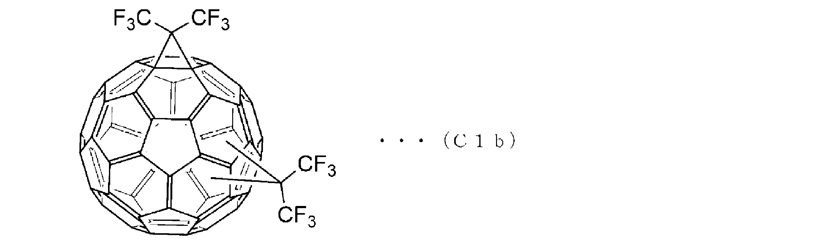
- the chemical formula of compound 1a is shown as (C1a)
- the chemical formula of compound 1b is shown as (C1b).
- Compound 1b is a mixture of isomers having different positions to which the substituent is added.
- Example 1-1 Thermogravimetric analysis of compound 1a in vacuum was carried out in order to confirm whether or not the compound 1a could be vapor-deposited by sublimation and the sublimation temperature.
- the sample (about 5 mg) was set in a vacuum thermogravimetric analyzer (VPE-9000 manufactured by Advance Riko Co., Ltd.). The temperature was raised from room temperature to 1000 ° C. at a rate of 10 ° C./min in a vacuum of 1 Pa or less.
- Ts ° C.
- -10% the temperature when the weight decreased by 50% was defined as Ts (° C.) (-50%).
- the results are shown in Table 1.
- Example 1 (Examples 1-2 to 1-6, Comparative Examples 1-1 to 1-4) Thermogravimetric analysis was carried out in the same manner as in Example 1 except that the compounds shown in Table 1 were used instead of the compound 1a. The results are shown in Table 1.
- the fullerene derivative of the present invention is the unsubstituted fullerene (C 60 ) of Comparative Example 1-1. It can be seen that sublimation is possible at a lower temperature. Further, when Example 1-6 having a fullerene skeleton of C 70 is compared with Comparative Example 1-4, it can be seen that the same tendency is observed even if the fullerene skeleton is C 70 .
- the fullerene derivative of the present invention is at a lower temperature than the fullerene derivative conventionally known to sublimate. It turns out that it can be sublimated.
- Example 2-1 Compound 1a was vapor-deposited on a glass substrate, and the absorption characteristics of the vapor-deposited thin film were evaluated.
- the thin film was prepared by depositing the thin film on a dry glass substrate washed with isopropyl alcohol (IPA) and acetone using an ultrasonic washer at a rate of 0.1 to 1.0 ⁇ / s under high vacuum.
- IPA isopropyl alcohol
- the absorption characteristics were evaluated by the absorption coefficient at 450 nm using a UV-Vis spectrophotometer (UV-2400 manufactured by Shimadzu Corporation). The results are shown in Table 2.
- Example 2-2 to 2-6 Comparative Examples 2-1 to 2-2
- the absorption characteristics were evaluated in the same manner as in Example 2-1 except that the compounds shown in Table 2 were used instead of the compound 1a. The results are shown in Table 2.
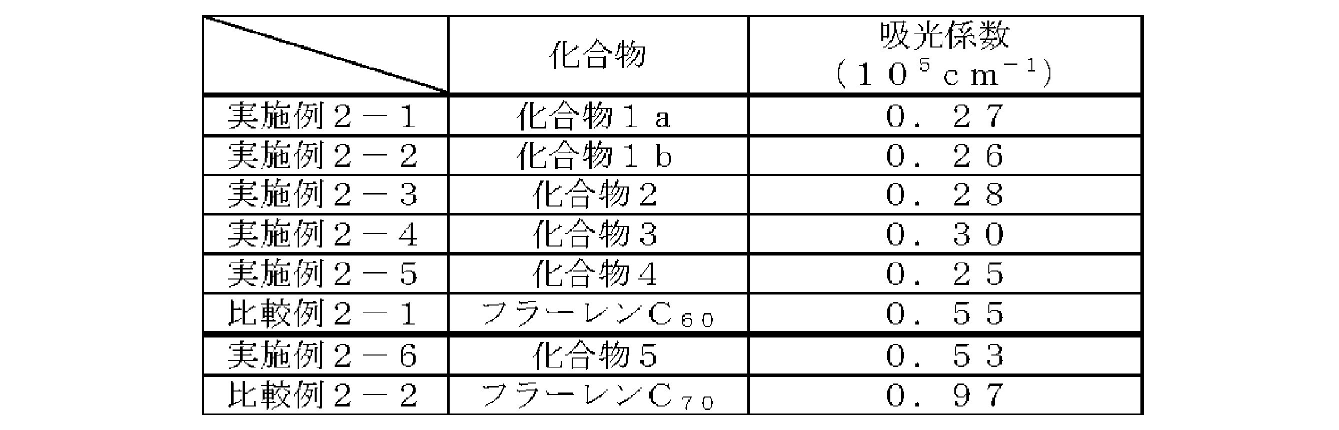
- the thin film containing the fullerene derivative in which the fullerene skeleton of the present invention is C 60 is compared with the thin film containing the unsubstituted fullerene C 60 (Comparative Example 2-1). It can be seen that the extinction coefficient at 450 nm is small. Further, the thin film containing a fullerene derivative having a fullerene skeleton of C 70 (Example 2-6) of the present invention absorbs light at 450 nm as compared with a thin film containing an unsubstituted fullerene C 70 (Comparative Example 2-2). It can be seen that the coefficient is small. From this, it can be confirmed that the fullerene derivative of the present invention does not exhibit abnormal absorption characteristics in the short wavelength region of visible light due to aggregation.
- fullerene derivative that can be synthesized without the need for a special synthesis device and can be vapor-deposited at a low temperature without thermal decomposition.
- the fullerene derivative of the present invention can be preferably used for a photoelectric element, a solid-state image pickup device, or the like.
Landscapes
- Chemical & Material Sciences (AREA)
- Organic Chemistry (AREA)
- Engineering & Computer Science (AREA)
- Materials Engineering (AREA)
- Nanotechnology (AREA)
- Inorganic Chemistry (AREA)
- Chemical Kinetics & Catalysis (AREA)
- Physics & Mathematics (AREA)
- Electromagnetism (AREA)
- Organic Low-Molecular-Weight Compounds And Preparation Thereof (AREA)
- Carbon And Carbon Compounds (AREA)
- Solid State Image Pick-Up Elements (AREA)
- Light Receiving Elements (AREA)
- Electroluminescent Light Sources (AREA)
Abstract
Description
本願は、2020年12月9日に、日本に出願された特願2020-204606号に基づき優先権を主張し、その内容をここに援用する。
また、非特許文献1に記載のジフルオロメタノ構造を有するフラーレン誘導体は、昇華温度が高く実用的ではない。
本発明の第一の態様は、以下のフラーレン誘導体を提供する。
フラーレン骨格と、
下記一般式(1)
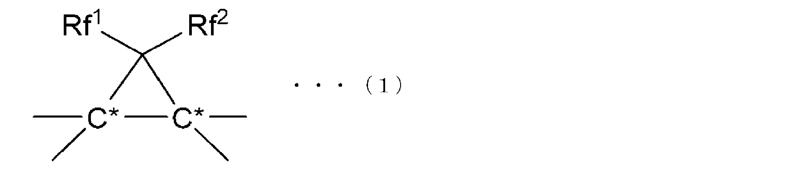
(式(1)中、C*はそれぞれ前記フラーレン骨格を形成する互いに隣り合った炭素原子であり、Rf1およびRf2はそれぞれ独立に炭素数1~4のパーフルオロアルキル基であり、Rf1およびRf2は互いに連結して環構造を形成してもよい。)
で示される部分構造と、を有するフラーレン誘導体。
本発明の第一の態様のフラーレン誘導体は、以下の特徴を有することが好ましい。以下の特徴は2つ以上を組み合わせることも好ましい。
[2] 前記フラーレン骨格が、C60、C70、C74、C76、又はC78である前
項[1]に記載のフラーレン誘導体。
[3] 前記Rf1およびRf2がトリフルオロメチル基である前項[1]または[2]に記載のフラーレン誘導体。
[4] 前記式(1)で示される部分構造が、1つのフラーレン骨格に対して1つ含まれる、前項[1]~[3]のいずれか一項に記載のフラーレン誘導体。
[5] 前項[1]~[4]のいずれか一項に記載のフラーレン誘導体を含む薄膜。
本発明の第二の態様は、以下の光電変換素子を提供する。
[6] 互いに対向する第1電極と第2電極と、
前記2つの電極の間に配置される有機層と、を有し、
前記有機層は、前項[1]~[4]のいずれか一項に記載のフラーレン誘導体を含む、光電変換素子。
本発明の第三の態様は、以下の固体撮像装置を提供する。
[7] 前項[6]に記載の光電変換素子を有する固体撮像装置。
本発明の第四の態様は、以下のフラーレン誘導体の製造方法を提供する。
[8] 前項[1]~[4]のいずれかに記載のフラーレン誘導体の製造方法であって、
フラーレンと下記式(2)

(式(2)中、Xはハロゲン原子を表し、Rf1およびRf2は前記式(1)で示されるものと同じである。)
で表される化合物を、塩基の存在下に反応させる工程を有する、フラーレン誘導体の製造方法。
本実施形態のフラーレン誘導体は、フラーレン骨格に式(1)で表される部分構造を有する化合物である。なお、本実施形態において「フラーレン誘導体」とは、これらのフラーレン骨格に対して特定の基が付加した構造を有する化合物を意味し、「フラーレン骨格」とはフラーレン由来の閉殻構造を構成する炭素骨格をいう。

(式(1)中、C*はそれぞれフラーレン骨格を形成する互いに隣り合った炭素原子であり、Rf1およびRf2はそれぞれ独立に炭素数1~4のパーフルオロアルキル基であり、Rf1およびRf2は互いに連結して環構造を形成してもよい。)
本実施形態のフラーレン誘導体の製造方法は、特に限定されないが、例えば以下の方法が挙げられる。すなわち、フラーレンと式(2)で示される化合物とを塩基の存在下に反応させ、前記式(1)で示されるフラーレン誘導体を得る。

(式(2)中、Xはハロゲン原子を表し、Rf1およびRf2は前記式(1)に示されるものと同じである。)
また、塩基の溶媒への溶解性を高め、反応速度を高める目的で、相間移動触媒を用いてもよい。相間移動触媒としては例えば、18-クラウン-6-エーテルや15-クラウン-5-エーテルなどのクラウンエーテル類、ポリエチレングリコールジメチルエーテルなどのポリアルキレングリコール類が挙げられる。反応速度を高める効果が強いことからクラウンエーテル類が好ましく、15-クラウン-5-エーテルが特に好ましい。前記相間移動触媒は、一種類のみを用いても良く、あるいは2種以上を組み合わせて使用してもよい。前記塩基の量は任意に選択でき、例えば、式(2)で表される化合物に対して、0.01~500モル当量などが例として挙げられる。
フラーレンと、式(2)で示される化合物と、塩基と、溶媒を混合する順番は、任意に選択できる。例えば、フラーレンを溶剤に溶解し、その後、式(2)で示される化合物と塩基とをさらに加えて、混合しても良い。ただしこの例のみに限定されない。
本実施形態の薄膜は、前記フラーレン誘導体を含む。薄膜は、スピンコートやスリットコートなどの湿式による成膜方法や、蒸着などの乾式による成膜方法など、どのような方法で形成されても構わないが、蒸着によって形成されることが好ましい。
薄膜は、本実施形態のフラーレン誘導体のみで構成されていてもよいし、他の化合物と混合された状態で構成されていてもよい。
本実施形態の光電変換素子は、互いに対向する第1電極と第2電極と、前記2つの電極の間に配置される有機層とを有する。前記有機層は、前記式(1)で表されるフラーレン誘導体を含む。また、前記有機層は前記フラーレン誘導体の他に、他の化合物を含んでもよい。前記第1電極および前記第2電極は特に限定されず、既知の材料等が使用できる。
また、前記本実施形態の光電変換素子は、上記のような特徴を有していればその構造は特に限定されない。光電変換素子の構造としては、例えば、特許文献2などに記載の素子構造が挙げられる。
本実施形態の固体撮像装置(イメージセンサ)は、前記光電変換素子を一つ以上有する。また、固体撮像装置は多様な電子装置に適用され、例えばモバイルホン、デジタルカメラなどに好ましく適用され得るが、これらに限定されるものではない。
50mLのナスフラスコ中で、C60(216mg,0.3mmol)を1,2-ジクロロベンゼン(20mL)に溶解させ、氷浴で冷却した。これに、カリウム-tert-ブトキシド(67mg,0.6mmol)、1,1,1,3,3,3-ヘキサフルオロ-2-ヨードプロパン(92mg,0.33mmol)、15-クラウン-5-エーテル(264mg,1.2mmol)を加えた後、氷浴で冷却しながら攪拌し、6時間反応させた。反応は常圧で行った。反応後、反応混合物を分取HPLC(カラム:ナカライテスク社製COSMOSIL PBB(内径20mm,長さ250mm)、溶離液:トルエン)で精製し、化合物1aを含むフラクションと、化合物1bを含むフラクションとを得た。それぞれ溶媒を留去し、得られた固体をメタノールで洗浄し、乾燥することにより、化合物1a84mgおよび化合物1b40mg、それぞれを茶褐色の固体として得た。以下に、化合物1aの化学式を(C1a)、化合物1bの化学式を(C1b)、としてそれぞれ示す。なお、化合物1bは置換基が付加している位置が異なる異性体の混合物である。

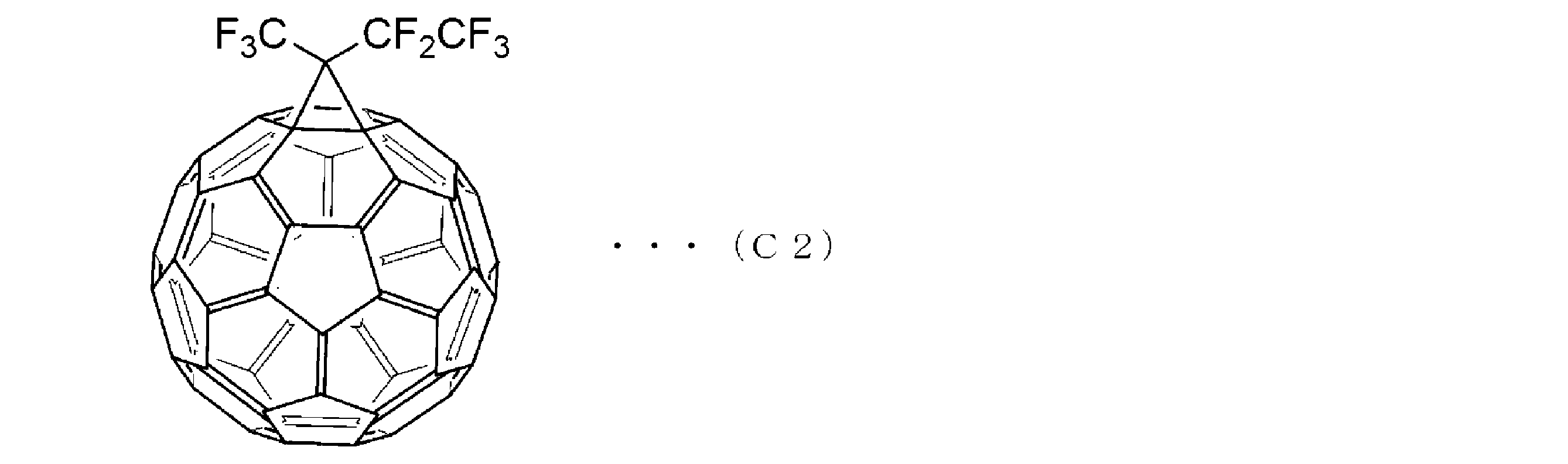
1,1,1,3,3,3-ヘキサフルオロ-2-ヨードプロパンに替えて、1,1,1,3,3,4,4,4-オクタフルオロ-2-ヨードブタンを同一モル量用いた以外は、合成例1と同様に合成を行い、化合物2を茶褐色の固体として79mg得た。以下に、化合物2の化学式を(C2)として示す。
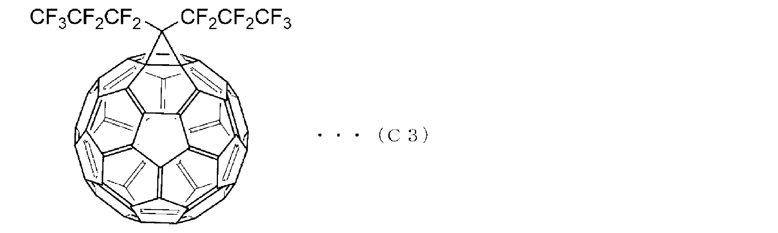
1,1,1,3,3,3-ヘキサフルオロ-2-ヨードプロパンに替えて、1,1,1,2,2,3,3,5,5,6,6,7,7,7-テトラデカフルオロ-4-ヨードヘプタンを同一モル量用いた以外は、合成例1と同様に合成を行い、化合物3を茶褐色の固体として91mg得た。以下に、化合物3の化学式を(C3)として示す。
1,1,1,3,3,3-ヘキサフルオロ-2-ヨードプロパンに替えて、2,2,3,3,4,4,5,5,6,6-デカフルオロ-1-ヨードシクロヘキサンを同一モル量用いた以外は、合成例1と同様に合成を行い、化合物4を茶褐色の固体として80mg得た。以下に、化合物4の化学式を(C4)として示す。

C60に替えて、C70を同一モル量用いた以外は合成例1と同様に合成を行い、化合物5を茶褐色の固体として68mg得た。以下に、化合物5の化学式を(C5)として示す。
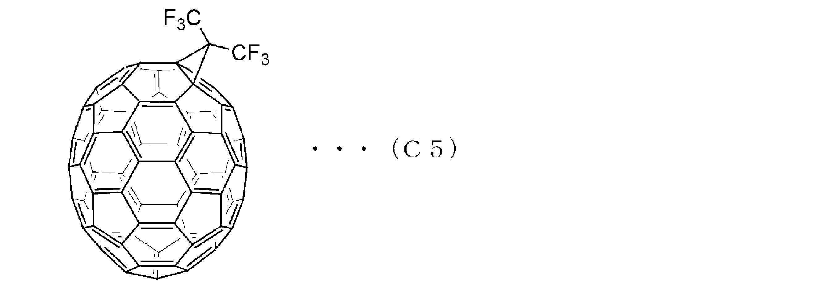
非特許文献1に記載されている方法で、化合物6(C6)を得た。以下に、化合物6の化学式を(C6)として示す。

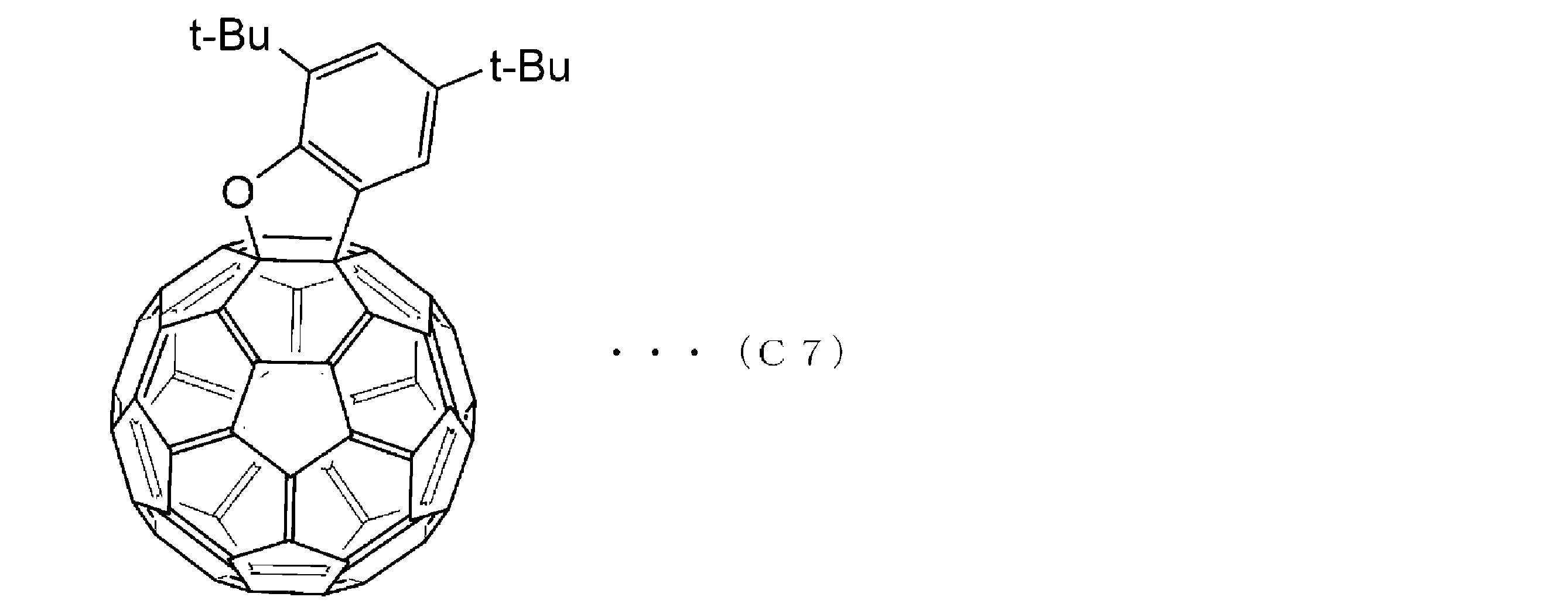
特許文献1の合成例1の方法で、化合物7(C7)を得た。以下に、化合物7の化学式を(C7)として示す。
化合物1aの昇華による蒸着の可否および、昇華温度を確認するために、真空中における化合物1aの熱重量分析を実施した。試料(約5mg)を真空熱重量分析装置(アドバンス理工社製VPE-9000)にセットした。1Pa以下の真空中において、室温から1000℃まで10℃/分の速度で昇温させた。試料の重量が当初の重量に対して10%低下したときの温度をTs(℃)(-10%)、50%低下したときの温度をTs(℃)(-50%)とした。結果を表1に示す。
化合物1aに代えて、表1に記載の化合物を用いた以外は実施例1と同様に、熱重量分析を実施した。結果を表1に示す。

ガラス基板上に化合物1aを蒸着し、蒸着された薄膜の吸光特性を評価した。前記薄膜は、超音波洗浄器を用いてイソプロピルアルコール(IPA)及びアセトンで洗浄した乾燥ガラス基板上に、高真空下、0.1~1.0Å/sの速度で蒸着させることによって作製した。吸光特性は、UV-Vis分光光度計(島津製作所製UV-2400)を用いて、450nmにおける吸光係数により評価した。結果は表2に示した。
化合物1aに代えて、表2に記載の化合物を用いた以外は実施例2-1と同様に吸光特性を評価した。結果を表2に示す。
本発明のフラーレン誘導体は、光電素子や固体撮像装置等に好ましく用いることができる。
Claims (16)
- フラーレン骨格と、
下記一般式(1)
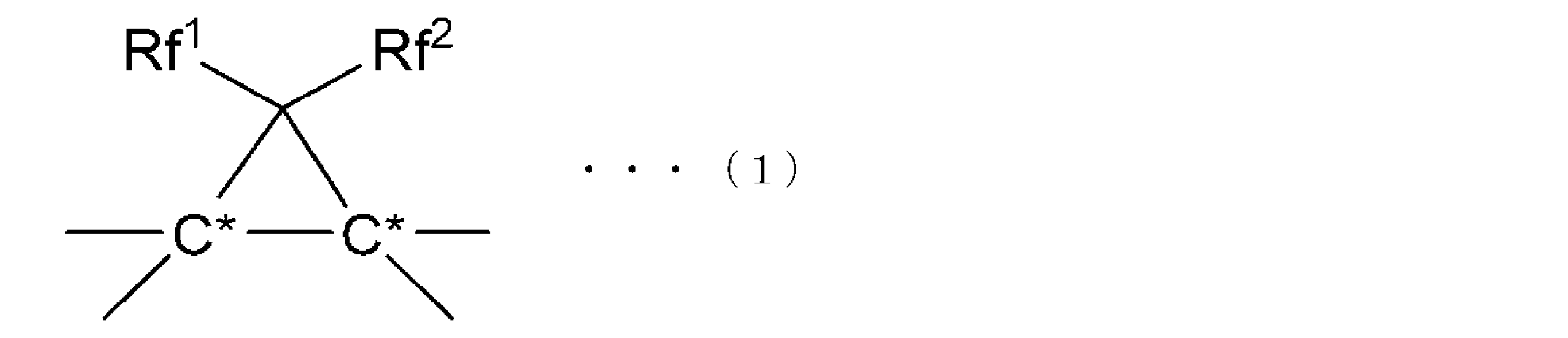
(式(1)中、C*はそれぞれ前記フラーレン骨格を形成する互いに隣り合った炭素原子であり、Rf1およびRf2はそれぞれ独立に炭素数1~4のパーフルオロアルキル基であり、Rf1およびRf2は互いに連結して環構造を形成してもよい。)
で示される部分構造を有するフラーレン誘導体。 - 前記フラーレン骨格が、C60、C70、C74、C76、又はC78である請求項1
に記載のフラーレン誘導体。 - 前記Rf1およびRf2がトリフルオロメチル基である請求項1または2に記載のフラーレン誘導体。
- 前記式(1)で示される部分構造が1つのフラーレン骨格に対して1つ含まれる、請求項1~3のいずれか一項に記載のフラーレン誘導体。
- 請求項1~4のいずれか一項に記載のフラーレン誘導体を含む薄膜。
- 互いに対向する第1電極と第2電極と、
前記2つの電極の間に配置される有機層と、を有し、
前記有機層は、請求項1~4のいずれか一項に記載のフラーレン誘導体を含む
光電変換素子。 - 請求項6に記載の光電変換素子を有する固体撮像装置。
- 請求項1~4のいずれかに記載のフラーレン誘導体の製造方法であって、
フラーレンと下記式(2)

(式(2)中、Xはハロゲン原子を表し、Rf1およびRf2は前記式(1)で示されるものと同じである。)
で表される化合物を塩基の存在下に反応させる工程を含む、フラーレン誘導体の製造方法。 - 前記塩基が、金属水酸化物、金属炭酸塩、金属アルコキシド、ピリジン、トリエチルアミン、ジアザビシクロウンデセンからなる群から選択される少なくとも1つである、請求項8に記載のフラーレン誘導体の製造方法。
- 前記塩基が、水酸化ナトリウム、水酸化カリウム、炭酸ナトリウム、炭酸カリウム、炭酸セシウム、ナトリウムエトキシド、カリウムエトキシド、カリウム-tert-ブトキシド、ピリジン、トリエチルアミン、ジアザビシクロウンデセンからなる群から選択される少なくとも1つである、請求項9に記載のフラーレン誘導体の製造方法。
- 前記Xがヨウ素である、請求項8~10のいずれか一項に記載のフラーレン誘導体の製造方法。
- 前記フラーレンが、C60、C70、C74、C76、又はC78である、請求項8~11のいずれか一項に記載のフラーレン誘導体の製造方法。
- 前記フラーレンと前記式(2)で示される化合物を反応させる工程に、相間移動触媒が使用される、請求項8~12のいずれか一項に記載のフラーレン誘導体の製造方法。
- 前記相間移動触媒が、18-クラウン-6-エーテル、15-クラウン-5-エーテル、ポリエチレングリコールジメチルエーテルからなる群から選択される少なくとも1つである、請求項13に記載のフラーレン誘導体の製造方法。
- 前記フラーレンと前記式(2)で示される化合物を反応させる工程が、-50℃から50℃の温度で行われる、請求項8~14のいずれか一項に記載のフラーレン誘導体の製造方法。
- 前記フラーレンと前記式(2)で示される化合物を反応させる工程の前に、前記フラーレンを溶媒と混合する工程を有する、請求項8~15のいずれか一項に記載のフラーレン誘導体の製造方法。
Priority Applications (5)
| Application Number | Priority Date | Filing Date | Title |
|---|---|---|---|
| KR1020237018924A KR102876092B1 (ko) | 2020-12-09 | 2021-12-06 | 풀러렌 유도체 및 그 제조 방법 |
| JP2022558041A JP7212227B2 (ja) | 2020-12-09 | 2021-12-06 | フラーレン誘導体およびその製造方法 |
| US18/039,311 US20240306486A1 (en) | 2020-12-09 | 2021-12-06 | Fullerene derivative and production method therefor |
| CN202180081730.7A CN116568660A (zh) | 2020-12-09 | 2021-12-06 | 富勒烯衍生物及其制造方法 |
| JP2022198035A JP7728738B2 (ja) | 2020-12-09 | 2022-12-12 | フラーレン誘導体 |
Applications Claiming Priority (2)
| Application Number | Priority Date | Filing Date | Title |
|---|---|---|---|
| JP2020-204606 | 2020-12-09 | ||
| JP2020204606 | 2020-12-09 |
Publications (1)
| Publication Number | Publication Date |
|---|---|
| WO2022124273A1 true WO2022124273A1 (ja) | 2022-06-16 |
Family
ID=81974416
Family Applications (1)
| Application Number | Title | Priority Date | Filing Date |
|---|---|---|---|
| PCT/JP2021/044774 Ceased WO2022124273A1 (ja) | 2020-12-09 | 2021-12-06 | フラーレン誘導体およびその製造方法 |
Country Status (5)
| Country | Link |
|---|---|
| US (1) | US20240306486A1 (ja) |
| JP (2) | JP7212227B2 (ja) |
| KR (1) | KR102876092B1 (ja) |
| CN (1) | CN116568660A (ja) |
| WO (1) | WO2022124273A1 (ja) |
Cited By (1)
| Publication number | Priority date | Publication date | Assignee | Title |
|---|---|---|---|---|
| WO2024117115A1 (ja) * | 2022-12-01 | 2024-06-06 | 三菱商事株式会社 | フラーレン誘導体、薄膜、光電変換素子、固体撮像装置及びフラーレン誘導体の製造方法 |
Families Citing this family (2)
| Publication number | Priority date | Publication date | Assignee | Title |
|---|---|---|---|---|
| US20240306486A1 (en) * | 2020-12-09 | 2024-09-12 | Resonac Corporation | Fullerene derivative and production method therefor |
| JP2025129653A (ja) * | 2024-02-26 | 2025-09-05 | 株式会社レゾナック | フラーレン誘導体、フラーレン誘導体の製造方法、薄膜、光電変換素子及び固体撮像装置 |
Citations (8)
| Publication number | Priority date | Publication date | Assignee | Title |
|---|---|---|---|---|
| WO2011033974A1 (ja) * | 2009-09-18 | 2011-03-24 | コニカミノルタホールディングス株式会社 | タンデム型有機光電変換素子、および太陽電池 |
| WO2011033973A1 (ja) * | 2009-09-18 | 2011-03-24 | コニカミノルタホールディングス株式会社 | 有機光電変換素子、および太陽電池 |
| JP2013140923A (ja) * | 2011-12-06 | 2013-07-18 | Osaka Univ | 有機半導体薄膜、及び有機薄膜太陽電池 |
| JP2016178130A (ja) * | 2015-03-18 | 2016-10-06 | ダイキン工業株式会社 | フラーレン誘導体、及びn型半導体材料 |
| WO2016194630A1 (ja) * | 2015-05-29 | 2016-12-08 | ソニーセミコンダクタソリューションズ株式会社 | 光電変換素子および固体撮像装置 |
| JP2019099570A (ja) * | 2017-12-04 | 2019-06-24 | 三星電子株式会社Samsung Electronics Co.,Ltd. | フラーレン誘導体及びそれを含む薄膜、光電素子並びにイメージセンサ及び電子装置 |
| JP2019142775A (ja) * | 2016-06-23 | 2019-08-29 | ダイキン工業株式会社 | フラーレン誘導体、およびそれを含有する半導体材料、およびそれを含有する半導体薄膜 |
| WO2019182143A1 (ja) * | 2018-03-23 | 2019-09-26 | 住友化学株式会社 | 光電変換素子 |
Family Cites Families (2)
| Publication number | Priority date | Publication date | Assignee | Title |
|---|---|---|---|---|
| US5354926A (en) * | 1993-02-23 | 1994-10-11 | E. I. Du Pont De Nemours And Company | Fluoroalkylated fullerene compounds |
| US20240306486A1 (en) | 2020-12-09 | 2024-09-12 | Resonac Corporation | Fullerene derivative and production method therefor |
-
2021
- 2021-12-06 US US18/039,311 patent/US20240306486A1/en active Pending
- 2021-12-06 KR KR1020237018924A patent/KR102876092B1/ko active Active
- 2021-12-06 JP JP2022558041A patent/JP7212227B2/ja active Active
- 2021-12-06 WO PCT/JP2021/044774 patent/WO2022124273A1/ja not_active Ceased
- 2021-12-06 CN CN202180081730.7A patent/CN116568660A/zh active Pending
-
2022
- 2022-12-12 JP JP2022198035A patent/JP7728738B2/ja active Active
Patent Citations (8)
| Publication number | Priority date | Publication date | Assignee | Title |
|---|---|---|---|---|
| WO2011033974A1 (ja) * | 2009-09-18 | 2011-03-24 | コニカミノルタホールディングス株式会社 | タンデム型有機光電変換素子、および太陽電池 |
| WO2011033973A1 (ja) * | 2009-09-18 | 2011-03-24 | コニカミノルタホールディングス株式会社 | 有機光電変換素子、および太陽電池 |
| JP2013140923A (ja) * | 2011-12-06 | 2013-07-18 | Osaka Univ | 有機半導体薄膜、及び有機薄膜太陽電池 |
| JP2016178130A (ja) * | 2015-03-18 | 2016-10-06 | ダイキン工業株式会社 | フラーレン誘導体、及びn型半導体材料 |
| WO2016194630A1 (ja) * | 2015-05-29 | 2016-12-08 | ソニーセミコンダクタソリューションズ株式会社 | 光電変換素子および固体撮像装置 |
| JP2019142775A (ja) * | 2016-06-23 | 2019-08-29 | ダイキン工業株式会社 | フラーレン誘導体、およびそれを含有する半導体材料、およびそれを含有する半導体薄膜 |
| JP2019099570A (ja) * | 2017-12-04 | 2019-06-24 | 三星電子株式会社Samsung Electronics Co.,Ltd. | フラーレン誘導体及びそれを含む薄膜、光電素子並びにイメージセンサ及び電子装置 |
| WO2019182143A1 (ja) * | 2018-03-23 | 2019-09-26 | 住友化学株式会社 | 光電変換素子 |
Cited By (1)
| Publication number | Priority date | Publication date | Assignee | Title |
|---|---|---|---|---|
| WO2024117115A1 (ja) * | 2022-12-01 | 2024-06-06 | 三菱商事株式会社 | フラーレン誘導体、薄膜、光電変換素子、固体撮像装置及びフラーレン誘導体の製造方法 |
Also Published As
| Publication number | Publication date |
|---|---|
| JP7212227B2 (ja) | 2023-01-25 |
| JPWO2022124273A1 (ja) | 2022-06-16 |
| KR102876092B1 (ko) | 2025-10-24 |
| US20240306486A1 (en) | 2024-09-12 |
| KR20230104242A (ko) | 2023-07-07 |
| JP2023057076A (ja) | 2023-04-20 |
| JP7728738B2 (ja) | 2025-08-25 |
| CN116568660A (zh) | 2023-08-08 |
Similar Documents
| Publication | Publication Date | Title |
|---|---|---|
| JP7728738B2 (ja) | フラーレン誘導体 | |
| TWI672311B (zh) | 新穎的化合物以及包含此化合物的有機發光裝置 | |
| EP4273151A1 (en) | Novel compound and organic light emitting device using same | |
| JP7536392B2 (ja) | 新規な化合物およびこれを利用した有機発光素子 | |
| JP7562218B2 (ja) | 新規な化合物およびこれを利用した有機発光素子 | |
| JP7580850B2 (ja) | 新規な化合物およびこれを利用した有機発光素子 | |
| CN110903295A (zh) | 一种以苯并呋喃衍生物为核心的有机化合物及其应用 | |
| CN115884962A (zh) | 用于制备氘化芳族化合物的方法和氘化反应组合物 | |
| CN117813290A (zh) | 新的化合物和包含其的有机发光器件 | |
| CN115667248A (zh) | 新型化合物及包含其的有机发光器件 | |
| JP7712024B2 (ja) | 新規な化合物およびこれを利用した有機発光素子 | |
| EP4242214A1 (en) | Novel compound and organic light emitting device using same | |
| CN116724677A (zh) | 有机发光器件 | |
| EP3904346B1 (en) | Novel compound and organic light emitting device comprising same | |
| CN115190879A (zh) | 新的化合物和包含其的有机发光器件 | |
| CN115135652B (zh) | 新化合物和包含其的有机发光器件 | |
| CN113272288B (zh) | 新的化合物和包含其的有机发光器件 | |
| KR102770369B1 (ko) | 신규한 화합물 및 이를 이용한 유기 발광 소자 | |
| JP2025129653A (ja) | フラーレン誘導体、フラーレン誘導体の製造方法、薄膜、光電変換素子及び固体撮像装置 | |
| EP4137472B1 (en) | Novel compound and organic light-emitting device comprising the same | |
| WO2024117115A1 (ja) | フラーレン誘導体、薄膜、光電変換素子、固体撮像装置及びフラーレン誘導体の製造方法 | |
| JP7612279B2 (ja) | 新規な化合物およびこれを利用した有機発光素子 | |
| EP3778582B1 (en) | Novel compound, coating composition comprising the same and organic light emitting device comprising the same | |
| JP2024523813A (ja) | 新規な化合物およびこれを含む有機発光素子 | |
| CN121248526B (zh) | 一种电子传输层材料、制备方法及包含其的有机电致发光器件 |
Legal Events
| Date | Code | Title | Description |
|---|---|---|---|
| 121 | Ep: the epo has been informed by wipo that ep was designated in this application |
Ref document number: 21903373 Country of ref document: EP Kind code of ref document: A1 |
|
| ENP | Entry into the national phase |
Ref document number: 2022558041 Country of ref document: JP Kind code of ref document: A |
|
| WWE | Wipo information: entry into national phase |
Ref document number: 18039311 Country of ref document: US |
|
| ENP | Entry into the national phase |
Ref document number: 20237018924 Country of ref document: KR Kind code of ref document: A |
|
| WWE | Wipo information: entry into national phase |
Ref document number: 202180081730.7 Country of ref document: CN |
|
| NENP | Non-entry into the national phase |
Ref country code: DE |
|
| 122 | Ep: pct application non-entry in european phase |
Ref document number: 21903373 Country of ref document: EP Kind code of ref document: A1 |