WO2022124121A1 - 保護素子 - Google Patents
保護素子 Download PDFInfo
- Publication number
- WO2022124121A1 WO2022124121A1 PCT/JP2021/043698 JP2021043698W WO2022124121A1 WO 2022124121 A1 WO2022124121 A1 WO 2022124121A1 JP 2021043698 W JP2021043698 W JP 2021043698W WO 2022124121 A1 WO2022124121 A1 WO 2022124121A1
- Authority
- WO
- WIPO (PCT)
- Prior art keywords
- switching element
- source
- switching
- drain
- gate
- Prior art date
- Legal status (The legal status is an assumption and is not a legal conclusion. Google has not performed a legal analysis and makes no representation as to the accuracy of the status listed.)
- Ceased
Links
Images





Classifications
-
- H—ELECTRICITY
- H10—SEMICONDUCTOR DEVICES; ELECTRIC SOLID-STATE DEVICES NOT OTHERWISE PROVIDED FOR
- H10D—INORGANIC ELECTRIC SEMICONDUCTOR DEVICES
- H10D89/00—Aspects of integrated devices not covered by groups H10D84/00 - H10D88/00
- H10D89/60—Integrated devices comprising arrangements for electrical or thermal protection, e.g. protection circuits against electrostatic discharge [ESD]
- H10D89/601—Integrated devices comprising arrangements for electrical or thermal protection, e.g. protection circuits against electrostatic discharge [ESD] for devices having insulated gate electrodes, e.g. for IGFETs or IGBTs
- H10D89/811—Integrated devices comprising arrangements for electrical or thermal protection, e.g. protection circuits against electrostatic discharge [ESD] for devices having insulated gate electrodes, e.g. for IGFETs or IGBTs using FETs as protective elements
- H10D89/813—Integrated devices comprising arrangements for electrical or thermal protection, e.g. protection circuits against electrostatic discharge [ESD] for devices having insulated gate electrodes, e.g. for IGFETs or IGBTs using FETs as protective elements specially adapted to provide an electrical current path other than the field-effect induced current path
- H10D89/815—Integrated devices comprising arrangements for electrical or thermal protection, e.g. protection circuits against electrostatic discharge [ESD] for devices having insulated gate electrodes, e.g. for IGFETs or IGBTs using FETs as protective elements specially adapted to provide an electrical current path other than the field-effect induced current path involving a parasitic bipolar transistor triggered by the local electrical biasing of the layer acting as base region of said parasitic bipolar transistor
-
- H—ELECTRICITY
- H10—SEMICONDUCTOR DEVICES; ELECTRIC SOLID-STATE DEVICES NOT OTHERWISE PROVIDED FOR
- H10D—INORGANIC ELECTRIC SEMICONDUCTOR DEVICES
- H10D84/00—Integrated devices formed in or on semiconductor substrates that comprise only semiconducting layers, e.g. on Si wafers or on GaAs-on-Si wafers
- H10D84/80—Integrated devices formed in or on semiconductor substrates that comprise only semiconducting layers, e.g. on Si wafers or on GaAs-on-Si wafers characterised by the integration of at least one component covered by groups H10D12/00 or H10D30/00, e.g. integration of IGFETs
- H10D84/82—Integrated devices formed in or on semiconductor substrates that comprise only semiconducting layers, e.g. on Si wafers or on GaAs-on-Si wafers characterised by the integration of at least one component covered by groups H10D12/00 or H10D30/00, e.g. integration of IGFETs of only field-effect components
- H10D84/83—Integrated devices formed in or on semiconductor substrates that comprise only semiconducting layers, e.g. on Si wafers or on GaAs-on-Si wafers characterised by the integration of at least one component covered by groups H10D12/00 or H10D30/00, e.g. integration of IGFETs of only field-effect components of only insulated-gate FETs [IGFET]
-
- H—ELECTRICITY
- H10—SEMICONDUCTOR DEVICES; ELECTRIC SOLID-STATE DEVICES NOT OTHERWISE PROVIDED FOR
- H10D—INORGANIC ELECTRIC SEMICONDUCTOR DEVICES
- H10D84/00—Integrated devices formed in or on semiconductor substrates that comprise only semiconducting layers, e.g. on Si wafers or on GaAs-on-Si wafers
- H10D84/80—Integrated devices formed in or on semiconductor substrates that comprise only semiconducting layers, e.g. on Si wafers or on GaAs-on-Si wafers characterised by the integration of at least one component covered by groups H10D12/00 or H10D30/00, e.g. integration of IGFETs
- H10D84/82—Integrated devices formed in or on semiconductor substrates that comprise only semiconducting layers, e.g. on Si wafers or on GaAs-on-Si wafers characterised by the integration of at least one component covered by groups H10D12/00 or H10D30/00, e.g. integration of IGFETs of only field-effect components
- H10D84/83—Integrated devices formed in or on semiconductor substrates that comprise only semiconducting layers, e.g. on Si wafers or on GaAs-on-Si wafers characterised by the integration of at least one component covered by groups H10D12/00 or H10D30/00, e.g. integration of IGFETs of only field-effect components of only insulated-gate FETs [IGFET]
- H10D84/83125—Integrated devices formed in or on semiconductor substrates that comprise only semiconducting layers, e.g. on Si wafers or on GaAs-on-Si wafers characterised by the integration of at least one component covered by groups H10D12/00 or H10D30/00, e.g. integration of IGFETs of only field-effect components of only insulated-gate FETs [IGFET] the IGFETs characterised by having shared source or drain regions
Definitions
- This disclosure relates to a protective element.
- a protective element for protecting from electrostatic discharge ESD
- a protective element configured by an n-type MOSFET metal-oxide-semiconductor field-effect transistor
- Patent Document 1 metal-oxide-semiconductor field-effect transistor
- the protection element that solves the above-mentioned problems is composed of n-type MOSFETs, a plurality of switching elements arranged side by side in one direction while being connected in parallel to each other, and a backgate guard ring surrounding the plurality of switching elements.
- the plurality of switching elements include a first switching element, a second switching element, a third switching element, and a fourth switching element arranged side by side in order, and the backgate guard ring is the first switching element.
- the switching element comprises a third portion located next to the third switching element on the opposite side, and the source of the first switching element is closer to the first portion than the gate of the first switching element.
- the source of the second switching element is arranged closer to the second portion than the gate of the second switching element, and the source of the third switching element is the third switching element. It is located closer to the second part than the gate of.
- the back gate guard ring is arranged near the source of the first to third switching elements, the hold voltage of the protection element can be increased and the malfunction of the protection element can be suppressed. Further, since the second part of the backgate guard ring is arranged between the source of the second switching element and the source of the third switching element, the first to fourth switching elements are individually surrounded by the backgate guard ring. The area of the protective element can be reduced as compared with the configuration. Therefore, it is possible to suppress the malfunction of the protective element and reduce the size of the protective element.
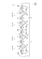
- FIG. 2 is a schematic cross-sectional view of the protective element of FIG.
- the characteristic diagram which shows the VI characteristic of a protection element.
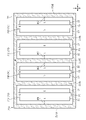
- Schematic cross-sectional view of the protective element of FIG. The plan view which shows a part of the protection element of another comparative example.
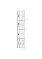
- the table which shows the area and hold voltage of the protection element of this embodiment and the protection element of a comparative example.
- the protection element 10 is, for example, a protection element that protects a pair of switching elements 201 and 202 of the inverter device 200 from ESD.
- the switching element 201 is, for example, a high-side switching element connected to a drive power supply
- the switching element 202 is a low-side switching element.
- Examples of the switching elements 201 and 202 include transistors such as MOSFETs and IGBTs. In the following description, a case where MOSFETs are used for the switching elements 201 and 202 will be described. In this embodiment, a p-type MOSFET is used for the switching element 201, and an n-type MOSFET is used for the switching element 202.
- the source of the switching element 201 is connected to the first electric wire L1, and the drain is connected to the drain of the switching element 202.
- the source of the switching element 202 is connected to the second electric wire L2. That is, the switching element 201 and the switching element 202 are connected in series between the first electric wire L1 and the second electric wire L2.
- the gates of the switching elements 201 and 202 are connected to a gate driver (not shown).
- the first electric wire L1 is an electric wire connected to the power supply terminal VDD connected to the drive power source
- the second electric wire L2 is an electric wire connected to the ground terminal GND.
- the protection element 10 is provided between the power supply terminal VDD and the ground terminal GND and the pair of switching elements 201 and 202, and causes a pair of currents flowing toward the pair of switching elements 201 and 202 due to static electricity. It is an element that flows instead of the switching elements 201 and 202.
- the protection element 10 includes a plurality of switching elements 20.
- Each switching element 20 is composed of an n-type MOSFET.
- the plurality of switching elements 20 are connected in parallel with each other. In one example, 10 or more and 20 or less switching elements 20 are connected in parallel. In this embodiment, 12 switching elements 20 are connected in parallel.
- the drain 21 of each switching element 20 is connected to the first electric wire L1, the source 22 is connected to the second electric wire L2, and the gate 23 is connected to the source 22. Further, the back gate 24 of each switching element 20 is connected to the source 22 of each switching element 20. Since the source 22 of each switching element 20 is connected to the second electric wire L2, each back gate 24 has a ground potential.
- the protection element 10 may be provided as a package separate from the pair of switching elements 201 and 202, or may be provided as a package integrated with the pair of switching elements 201 and 202. In the present embodiment, the protection element 10 is provided as a package different from the pair of switching elements 201 and 202, that is, a package composed of a plurality of switching elements 20.
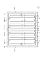
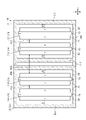
- FIG. 2 shows an example of an arrangement mode of a plurality of switching elements 20.
- FIG. 2 describes an arrangement mode of the four switching elements 20. Since the arrangement of the remaining eight switching elements 20 is the same as that in FIG. 2, the description thereof will be omitted. In FIG. 2, for convenience, switching elements 20 other than the four switching elements 20 are omitted.
- the four switching elements 20 will be referred to as a first switching element 20A, a second switching element 20B, a third switching element 20C, and a fourth switching element 20D.
- “D” is attached to the drain 21
- “S” is attached to the source 22
- “G” is attached to the gate 23
- the back gate 24 is attached.
- BG is attached to.
- the back gate 24 is provided with dot hatching.
- each switching element 20A to 20D is formed on the semiconductor substrate 30. That is, FIG. 2 is a plan view of the semiconductor substrate 30 as viewed from the thickness direction thereof.
- An example of the semiconductor substrate 30 is a Si (silicon) substrate.
- the switching elements 20A to 20D are arranged in one direction. In the following description, the direction in which the switching elements 20A to 20D are lined up is the x direction, the thickness direction of the semiconductor substrate 30 is the z direction, and the direction orthogonal to both the x direction and the z direction is the y direction. Further, "planar view" indicates a state viewed from the z direction.
- the switching elements 20A to 20D are arranged so as to be aligned with each other in the y direction and separated from each other in the x direction.
- the first switching element 20A, the second switching element 20B, the third switching element 20C, and the fourth switching element 20D are arranged side by side in this order in the x direction. That is, in the x direction, the second switching element 20B and the third switching element 20C are arranged between the first switching element 20A and the fourth switching element 20D.
- the second switching element 20B is arranged near the first switching element 20A with respect to the third switching element 20C.
- each switching element 20A to 20D are arranged side by side in the x direction. That is, the arrangement directions of the drain 21, the source 22, and the gate 23 of the switching elements 20A to 20D are the same as the arrangement directions of the switching elements 20A to 20D.
- the source 22, the gate 23, and the drain 21 are arranged in this order in the first switching element 20A, and the drain 21, the gate 23, and the source 22 are arranged in this order in the second switching element 20B. .. That is, the drain 21 of the first switching element 20A and the drain 21 of the second switching element 20B are arranged so as to be adjacent to each other in the x direction. Further, the source 22 of the first switching element 20A and the source 22 of the second switching element 20B are arranged so as to be farthest from each other.
- the arrangement of the drain 21, source 22, and gate 23 of the third switching element 20C and the fourth switching element 20D is the same as that of the first switching element 20A and the second switching element 20B. That is, in the third switching element 20C, the source 22, the gate 23, and the drain 21 are arranged in this order, and in the fourth switching element 20D, the drain 21, the gate 23, and the source 22 are arranged in this order. Therefore, the source 22 of the third switching element 20C and the source 22 of the second switching element 20B are arranged so as to be adjacent to each other in the x direction.
- the drain 21, source 22, and gate 23 of each of the switching elements 20A to 20D are arranged in the x direction so as to be aligned with each other in the y direction.
- the shapes of the drain 21, the source 22, and the gate 23 of the switching elements 20A to 20D in the plan view are strips extending in the y direction, respectively.
- the length of the drain 21 in the y direction is equal to the length of the source 22 in the y direction.
- the length of the gate 23 in the y direction is longer than the length of the drain 21 and the source 22 in the y direction. In a plan view, both ends of the gate 23 in the y direction protrude in the y direction with respect to the drain 21 and the source 22.
- the protection element 10 includes a back gate guard ring 25 that surrounds a plurality of switching elements 20.
- the back gate guard ring 25 shown in FIG. 2 surrounds each of the switching elements 20A to 20D, and is composed of the back gate 24 of each switching element 20A to 20D. That is, the back gate guard ring 25 is configured as a common back gate 24 for each of the switching elements 20A to 20D.
- the back gate guard ring 25 is arranged between the first portion 25A arranged next to the second switching element 20B on the opposite side of the first switching element 20A, and between the second switching element 20B and the third switching element 20C.
- the second portion 25B is provided, and the third portion 25C arranged on the side opposite to the third switching element 20C in the fourth switching element 20D is provided.
- the shapes of the first to third portions 25A to 25C in a plan view are strips extending in the y direction.
- the source 22 of the first switching element 20A is arranged closer to the first portion 25A than the gate 23 of the first switching element 20A.
- the drain 21 of the first switching element 20A is arranged closer to the second portion 25B than the gate 23 of the first switching element 20A.
- the drain 21 of the second switching element 20B is arranged closer to the first portion 25A than the gate 23 of the second switching element 20B.
- the source 22 of the second switching element 20B is arranged closer to the second portion 25B than the gate 23 of the second switching element 20B.
- the source 22 of the third switching element 20C is arranged closer to the second portion 25B than the gate 23 of the third switching element 20C.
- the drain 21 of the third switching element 20C is arranged closer to the third portion 25C than the gate 23 of the third switching element 20C.
- the drain 21 of the fourth switching element 20D is arranged closer to the second portion 25B than the gate 23 of the fourth switching element 20D.
- the source 22 of the fourth switching element 20D is arranged closer to the third portion 25C than the gate 23 of the fourth switching element 20D.
- the source 22, the gate 23, and the drain 21 are arranged in this order from the first portion 25A to the second portion 25B in the x direction.
- the drain 21, the gate 23, and the source 22 are arranged in this order from the first portion 25A to the second portion 25B in the x direction.
- the source 22, the gate 23, and the drain 21 are arranged in this order from the second portion 25B to the third portion 25C in the x direction.
- the drain 21, the gate 23, and the source 22 are arranged in this order from the second portion 25B to the third portion 25C in the x direction.
- the first portion 25A is arranged apart from the source 22 of the first switching element 20A in the x direction.
- the second portion 25B is arranged apart from both the source 22 of the second switching element 20B and the source 22 of the third switching element 20C in the x direction.
- the third portion 25C is arranged apart from the source 22 of the fourth switching element 20D in the x direction.
- the back gate guard ring 25 includes a pair of fourth portions 25D connecting both ends of the first to third portions 25A to 25C in the y direction.
- the shape of the pair of fourth portions 25D in a plan view is a band extending in the x direction.
- the pair of fourth portions 25D are arranged apart from the switching elements 20A to 20D in the y direction.
- the first switching element 20A and the second switching element 20B are surrounded by the first portion 25A, the second portion 25B, and the pair of fourth portions 25D.
- a third switching element 20C and a fourth switching element 20D are surrounded by a second portion 25B, a third portion 25C, and a pair of fourth portions 25D.
- the first to third portions 25A to 25C are each formed in a strip shape extending in the y direction.
- the first portion 25A is formed in a single band shape extending in a direction orthogonal to the arrangement direction of the plurality of switching elements 20.
- the second portion 25B is formed in a single band shape extending in a direction orthogonal to the arrangement direction of the plurality of switching elements 20.
- the third portion 25C is formed in a single band shape extending in a direction orthogonal to the arrangement direction of the plurality of switching elements 20.
- the angle formed by the direction in which the first portion 25A extends and the arrangement direction of the plurality of switching elements 20 is, for example, 85 ° or more and 95 ° or less, it is orthogonal to the arrangement direction of the plurality of switching elements 20. It can be said that it extends in the direction.
- the angle between the extending direction of the second portion 25B and the arrangement direction of the plurality of switching elements 20 is, for example, 85 ° or more and 95 ° or less
- the second portion 25B extends in a direction orthogonal to the arrangement direction of the plurality of switching elements 20. It can be said that it is.
- the third portion 25C extends in a direction orthogonal to the arrangement direction of the plurality of switching elements 20. It can be said that it is.
- the arrangement direction of the plurality of switching elements 20 can be defined by, for example, a line segment connecting the centers of the gates 23 of the switching elements 20 in the y direction.
- the second portion 25B arranged between the second switching element 20B and the third switching element 20C is formed by one, the second portion 25B is the source 22 of the second switching element 20B and the third switching.
- the back gate guard ring 25 is common to the source 22 of the element 20C.
- the sources 22 of the switching elements 20A to 20D and the first to third portions 25A to 25C are parallel to each other. That is, the distance between the source 22 of the first switching element 20A and the first portion 25A in the x direction is constant in the y direction, and between the source 22 of the second switching element 20B and the second portion 25B in the x direction. Is constant in the y direction, the distance between the source 22 of the third switching element 20C and the second portion 25B in the x direction is constant in the y direction, and the source 22 and the third of the fourth switching element 20D. The distance between the portion 25C and the x direction is constant in the y direction.
- the distance DS2 between the second switching element 20B and the third switching element 20C is the first switching element 20A.
- the distance between and the second switching element 20B is larger than DS1.
- the distance DS2 is larger than the distance DS3 between the third switching element 20C and the fourth switching element 20D.
- the distance D1 between the source 22 of the first switching element 20A and the first portion 25A is equal to the distance D2 between the source 22 of the second switching element 20B and the second portion 25B.
- the amount of deviation between the distance D1 and the distance D2 is, for example, within 10% of the distance D1, it can be said that the distance D1 and the distance D2 are equal.
- the distance D3 between the source 22 of the third switching element 20C and the second portion 25B is equal to the distance D2 between the source 22 of the second switching element 20B and the second portion 25B.
- the amount of deviation between the distance D3 and the distance D2 is, for example, within 10% of the distance D3, it can be said that the distance D3 and the distance D2 are equal.
- the distance D4 between the source 22 of the fourth switching element 20D and the third portion 25C is equal to the distance D2 between the source 22 of the second switching element 20B and the second portion 25B. That is, the distances D1 to D4 are equal to each other.
- the amount of deviation between the distance D4 and the distance D2 is, for example, within 10% of the distance D4, it can be said that the distance D4 and the distance D2 are equal. That is, the distance D1, the distance D2, the distance D3, and the distance D4 are equal to each other.
- the distances D1, D3, and D4 are equal to the distance D2, the distances D1 to D4 are equal to each other, but the distance is not limited to this, and a distance other than the distance D2 may be used as a reference. In one example, since the distances D2 to D4 are equal to the distance D1, the distances D1 to D4 may be equal to each other. Further, if the maximum deviation amount among the distances D1 to D4 is, for example, within 10% of the distance D1, it may be said that the distances D1 to D4 are equal to each other.
- the reference is set to the distance D1, but the distance is not limited to this, and any of the distances D2 to D4 may be used.
- the distances D1 to D4 are the distances between the drain 21 of the first switching element 20A and the drain 21 of the second switching element 20B, that is, between the first switching element 20A and the second switching element 20B. Equal to the distance DS1. Further, the distances D1 to D4 are the distance between the drain 21 of the third switching element 20C and the drain 21 of the fourth switching element 20D, that is, the distance DS3 between the third switching element 20C and the fourth switching element 20D. equal. The relationship between the distances D1 to D4 and the distances DS1 and DS3 can be arbitrarily changed. In one example, the distances DS1 and DS3 may be smaller than the distances D1 to D4.
- FIG. 3 shows a cross-sectional view of each switching element 20A to 20D.
- the semiconductor substrate 30 is a Si substrate having a p - type region 34.
- the p - type region 34 is formed on the semiconductor substrate 30 as, for example, a well region.
- a drain 21 and a source 22 of each switching element 20A to 20D and a back gate guard ring 25 are formed on the surface 31 of the semiconductor substrate 30, a drain 21 and a source 22 of each switching element 20A to 20D and a back gate guard ring 25 are formed.
- the drain 21 and the source 22 are formed by an n + type well region.
- the backgate guard ring 25 is formed by a p + -shaped well region.
- gates 23 of the switching elements 20A to 20D are formed via the oxide film 32.
- An example of the oxide film 32 is silicon oxide (SiO 2 ). That is, a plurality of oxide films 32 are formed on the surface 31 of the semiconductor substrate 30. The plurality of oxide films 32 are arranged apart from each other in the x direction. Each oxide film 32 is formed between the drain 21 and the source 22. A gate 23 is formed on each oxide film 32.
- An element separation band 33 is formed between the source 22 of the fourth switching element 20D and the third portion 25C, respectively.
- the element separation band 33 is, for example, STI or LOCOS.
- the drain 21 (n + ) and the source 22 (n + ) of the first switching element 20A and the p - type region 34 of the semiconductor substrate 30 constitute the first parasitic transistor 26A.
- the base of the first parasitic transistor 26A is connected to the first portion 25A of the backgate guard ring 25.
- the resistance RA between the base of the first parasitic transistor 26A and the first portion 25A is the resistance component of the p - type region 34.
- the second parasitic transistor 26B is composed of the drain 21 (n + ) and the source 22 (n + ) of the second switching element 20B and the p ⁇ type region 34, and the drain 21 (n + ) and the drain 21 (n +) of the third switching element 20C.
- the third parasitic transistor 26C is composed of the source 22 (n + ) and the p - type region 34.
- the base of each parasitic transistor 26B, 26C is connected to the second portion 25B of the backgate guard ring 25.
- the resistance RB between the base of the second parasitic transistor 26B and the second portion 25B and the resistance RC between the base of the third parasitic transistor 26C and the second portion 25B are resistance components of the p - type region 34, respectively. ..
- the fourth parasitic transistor 26D is configured from the drain 21 (n + ) and the source 22 (n + ) of the fourth switching element 20D and the p ⁇ type region 34.
- the base of the fourth parasitic transistor 26D is connected to the third portion 25C of the backgate guard ring 25.
- the resistance RD between the base of the fourth parasitic transistor 26D and the third portion 25C is the resistance component of the p - type region 34.
- the solid line graph in FIG. 4 is a characteristic diagram showing the IV characteristics of the protective element 10.
- the dot hatching region in which the voltage ranges from 0V to VS indicates the operating region of each of the switching elements 201 and 202 (see FIG. 1).
- the area of dot hatching where the voltage is equal to or higher than the voltage VDC indicates the area where the switching elements 201 and 202 fail.
- the voltage V between the electric wire L1 and the electric wire L2 fluctuates depending on the ESD.
- the protection element 10 protects the switching elements 201 and 202 from the fluctuating voltage V. More specifically, the protection element 10 needs to operate so that the voltage V is lower than the first voltage value VDC, which is the lower limit of the voltage at which the switching elements 201 and 202 are destroyed. Further, the protection element 10 needs to operate at a voltage higher than the second voltage value VDM, which is higher than the upper limit value of the voltage range, so as not to operate in the voltage range of the operating region of the switching elements 201, 202. That is, the protection element 10 needs to operate in a voltage range higher than the second voltage value VDM and lower than the first voltage value VDL.
- the second voltage value VDM is also referred to as an absolute maximum voltage.
- the hold voltage VH may decrease, and the second voltage value may be VDM or less.
- the resistance value of the resistance component of the p - type region 34 between the source 22 and the back gate 24 is considered to be proportional to the distance between the source 22 and the back gate 24. That is, as shown in FIG. 5, when the back gate guard ring 25X is formed so as to collectively surround each of the switching elements 20A to 20D, the source 22 of the second switching element 20B and the first back gate guard ring 25X are formed. The distance DX1 between the end 25XA and the distance DX2 between the source 22 of the third switching element 20C and the second end 25XB of the backgate guard ring 25X are increased, respectively. As shown in FIG.
- the resistance RX1 of the p - type region 34 between the source 22 of the second switching element 20B and the first end portion 25XA of the backgate guard ring 25X is the base of the second parasitic transistor 26B and the second resistance RX1. 1
- the resistance RX2 of the p - type region 34 between the source 22 of the third switching element 20C and the second end portion 25XB of the back gate guard ring 25X is the base of the third parasitic transistor 26C and the resistance RX2 of the fourth parasitic transistor 26D.
- increasing the back gate guard ring can be mentioned.
- the back gate guard ring 25X so as to individually surround each of the switching elements 20A to 20D.
- the distance DXA between the first end portion 25XA of the back gate guard ring 25X and the source 22 of the first switching element 20A, and the source of the first intermediate portion 25XC and the second switching element 20B of the back gate guard ring 25X is formed so as to individually surround each of the switching elements 20A to 20D.
- the distance between 22 and DXD is shortened respectively.
- the hold voltage VH (hold voltage VH in Comparative Example 2) is higher than the hold voltage VH in the case of the protection element of FIG. 5 (Comparative Example 1).
- the backgate guard ring 25X shown in FIG. 7 has a second intermediate portion 25XD between the switching element 20A and the switching element 20B, and a third intermediate portion 25XE between the switching element 20C and the switching element 20D. Therefore, as shown in FIG. 8, the area ratio of the protective element of Comparative Example 2 of FIG. 7 to the protective element of Comparative Example 1 of FIG. 5 is 1.61, and the area of the protective element of Comparative Example 2 is compared. It is larger than the area of the protective element of Example 1.
- the second intermediate portion 25XD is arranged between the drain 21 of the first switching element 20A and the drain 21 of the second switching element 20B
- the third intermediate portion 25XE is the drain 21 and the fourth of the third switching element 20C. Since it is arranged between the switching element 20D and the drain 21, both intermediate portions 25XD and 25XE do not substantially contribute to the improvement of the hold voltage VH.
- the back gate guard ring 25 has a first portion 25A arranged next to the source 22 of the first switching element 20A and a source 22 of the second switching element 20B.
- a second portion 25B arranged between the source 22 and the source 22 of the third switching element 20C, and a third portion 25C arranged next to the source 22 of the fourth switching element 20D are provided. That is, the back gate guard ring 25 of the present embodiment does not include the second intermediate portion 25XD and the third intermediate portion 25XE of the back gate guard ring 25X shown in FIG. 7. Therefore, as shown in FIG. 8, the area ratio of the protective element 10 of the present embodiment to the protective element of Comparative Example 1 of FIG.
- the protection element 10 includes a plurality of switching elements 20 composed of n-type MOSFETs arranged side by side in one direction while being connected in parallel to each other, and a back gate guard ring surrounding the plurality of switching elements 20. 25 and.
- the plurality of switching elements 20 include a first switching element 20A, a second switching element 20B, a third switching element 20C, and a fourth switching element 20D arranged side by side in order.
- the back gate guard ring 25 is arranged between the first portion 25A arranged next to the second switching element 20B on the opposite side of the first switching element 20A, and between the second switching element 20B and the third switching element 20C.
- the second portion 25B is provided, and the third portion 25C arranged next to the third switching element 20C on the opposite side of the fourth switching element 20D is provided.
- the source 22 of the first switching element 20A is arranged closer to the first portion 25A than the gate 23 of the first switching element 20A, and the source 22 of the second switching element 20B is the gate 23 of the second switching element 20B.
- the source 22 of the third switching element 20C is arranged closer to the second portion 25B than the gate 23 of the third switching element 20C.
- the back gate guard ring 25 is arranged near the source 22 of the first to third switching elements 20A to 20C, the hold voltage VH of the protection element 10 can be increased, and the protection element 10 can be increased. Malfunction can be suppressed.
- the second portion 25B of the back gate guard ring 25 is arranged between the source 22 of the second switching element 20B and the source 22 of the third switching element 20C, each switching element is as shown in FIG.
- the area of the protective element 10 can be reduced as compared with the configuration in which the 20A to 20D are individually surrounded by the back gate guard ring. Therefore, it is possible to suppress the malfunction of the protective element 10 and reduce the size of the protective element 10.
- the second portion 25B of the back gate guard ring 25 is formed in a single band shape extending in a direction (y direction) orthogonal to the arrangement direction (x direction) of the plurality of switching elements 20. ..
- the area of the protective element 10 in a plan view can be reduced as compared with a configuration in which a plurality of second portions 25B are provided. Therefore, the size of the protective element 10 can be reduced.
- the drains 21 of the switching elements 20A to 20D are individually provided. According to this configuration, the first switching element 20A and the second switching element 20B are provided as a common drain, and the third switching element 20C and the fourth switching element 20D are provided as a common drain.
- the volume of the drain 21 can be increased as compared with the above. Therefore, the current value that can be tolerated by the protection element 10 can be increased.
- the above embodiment is an example of possible embodiments of the protective element according to the present disclosure, and is not intended to limit the embodiments.
- the protective element according to the present disclosure may take a form different from the embodiment exemplified above.
- One example thereof is a form in which a part of the configuration of the above embodiment is replaced, changed, or omitted, or a new configuration is added to the above embodiment.
- the following modification examples can be combined with each other as long as they are not technically inconsistent.
- the parts common to the above embodiments are designated by the same reference numerals as those of the above embodiments, and the description thereof will be omitted.
- a plurality of second portions 25B of the back gate guard ring 25 may be provided.
- two second portions 25B of the back gate guard ring 25 are provided so as to be separated from each other in the x direction.
- the distance D3 between the third switching element 20C and the source 22 of the third switching element 20C is equal to each other.
- the distances D2 and D3 are the distance D1 between the source 22 of the first switching element 20A and the first portion 25A of the back gate guard ring 25, and the source 22 and the third portion 25C of the fourth switching element 20D. Equal to both of the distances D4 between.
- the drain 21 of the first switching element 20A and the drain 21 of the second switching element 20B may be provided as a common drain. This common drain corresponds to the first drain. Further, the drain 21 may be shared for the third switching element 20C and the fourth switching element 20D. The common drain of the third switching element 20C and the fourth switching element 20D corresponds to the second drain. According to this configuration, the area of the protection element 10 can be reduced as compared with the case where the drains 21 of the switching elements 20A to 20D are individually provided.
- the gate 23, the common drain 21, the gate 23 of the second switching element 20B, and the source 22 of the second switching element 20B are arranged in this order.
- the protection element 10 is a protection element for protecting the pair of switching elements 201 and 202, but the protection element 10 is not limited to this.
- the protection element 10 may be a protection element for protecting the LSI.
- the protective element 10 may be any protective element for electronic components such as semiconductor devices.
- a plurality of switching elements composed of n-type MOSFETs and arranged side by side in a row while being connected in parallel with each other.
- a back gate guard ring that surrounds the plurality of switching elements is provided.
- the plurality of switching elements include a first switching element and a second switching element.
- the backgate guard ring includes a first portion and a second portion. The first portion, the first switching element, the second switching element, and the second portion are arranged in this order.
- the source of the first switching element is arranged closer to the first portion than the gate of the first switching element.
- the source of the second switching element is a protection element arranged closer to the second portion than the gate of the second switching element.
- Appendix 2 The protection element according to Appendix 1, wherein the distance between the source of the first switching element and the first portion and the distance between the source of the second switching element and the second portion are equal to each other.
- Appendix 4 The protection element according to Appendix 3, wherein the drain, the gate, and the source of each of the switching elements are arranged along the arrangement direction of the plurality of switching elements.
- the source, gate, and drain of the first switching element are arranged in this order from the first portion to the second portion in the arrangement direction of the first switching element and the second switching element.
- the drain, gate, and source of the second switching element are arranged in this order from the first portion to the second portion in the arrangement direction of the first switching element and the second switching element.
- Appendix 6 The protective element according to Appendix 1 or 2, wherein the drain of the first switching element and the drain of the second switching element are provided as a common drain.
- Appendix 7 The protection element according to Appendix 6, wherein the source, the gate, and the common drain of each switching element are arranged along the arrangement direction of the plurality of switching elements.
Landscapes
- Semiconductor Integrated Circuits (AREA)
Abstract
Description
図1に示すように、保護素子10は、たとえばインバータ装置200の一対のスイッチング素子201,202をESDから保護する保護素子である。スイッチング素子201はたとえば駆動電源に接続されるハイサイドのスイッチング素子であり、スイッチング素子202はローサイドのスイッチング素子である。スイッチング素子201,202としてはたとえばMOSFETやIGBT等のトランジスタが挙げられる。なお、以降の説明では、スイッチング素子201,202にMOSFETが用いられた場合として説明する。本実施形態では、スイッチング素子201にはp型MOSFETが用いられており、スイッチング素子202にはn型MOSFETが用いられている。
平面視における各スイッチング素子20A~20Dのドレイン21、ソース22、およびゲート23の形状はそれぞれ、y方向に延びる帯状である。ドレイン21のy方向の長さは、ソース22のy方向の長さと等しい。ゲート23のy方向の長さは、ドレイン21およびソース22のy方向の長さよりも長い。平面視において、ゲート23のy方向の両端部は、ドレイン21およびソース22に対してy方向にはみ出している。
平面視において、各スイッチング素子20A~20Dのソース22と第1~第3部分25A~25Cとは平行である。つまり、第1スイッチング素子20Aのソース22と第1部分25Aとのx方向の間の距離はy方向において一定であり、第2スイッチング素子20Bのソース22と第2部分25Bとのx方向の間の距離はy方向において一定であり、第3スイッチング素子20Cのソース22と第2部分25Bとのx方向の間の距離はy方向において一定であり、第4スイッチング素子20Dのソース22と第3部分25Cとのx方向の間の距離はy方向において一定である。
図3に示すように、半導体基板30は、p-型領域34を有するSi基板である。p-型領域34は、たとえばウェル領域として半導体基板30に形成されている。半導体基板30の表面31には、各スイッチング素子20A~20Dのドレイン21およびソース22とバックゲートガードリング25とが形成されている。ドレイン21およびソース22は、n+型のウェル領域によって形成されている。バックゲートガードリング25は、p+型のウェル領域によって形成されている。
図4~図8を参照して、本実施形態の保護素子10の作用について説明する。なお、図8において、図5および図6に示す比較例の保護素子を比較例1とし、図7に示す比較例の保護素子を比較例2とする。
本実施形態の保護素子10によれば、以下の効果が得られる。
(1)保護素子10は、互いに並列に接続された状態で一方向に並んで配置されたn型のMOSFETによって構成された複数のスイッチング素子20と、複数のスイッチング素子20を囲むバックゲートガードリング25と、を備えている。複数のスイッチング素子20は、順に並んで配置された第1スイッチング素子20A、第2スイッチング素子20B、第3スイッチング素子20C、および第4スイッチング素子20Dを含む。バックゲートガードリング25は、第1スイッチング素子20Aにおける第2スイッチング素子20Bとは反対側の隣に配置された第1部分25Aと、第2スイッチング素子20Bと第3スイッチング素子20Cとの間に配置された第2部分25Bと、第4スイッチング素子20Dにおける第3スイッチング素子20Cとは反対側の隣に配置された第3部分25Cと、を備えている。第1スイッチング素子20Aのソース22は、第1スイッチング素子20Aのゲート23よりも第1部分25Aの近くに配置されており、第2スイッチング素子20Bのソース22は、第2スイッチング素子20Bのゲート23よりも第2部分25Bの近くに配置されており、第3スイッチング素子20Cのソース22は、第3スイッチング素子20Cのゲート23よりも第2部分25Bの近くに配置されている。
この構成によれば、第1スイッチング素子20Aと第2スイッチング素子20Bとが共通のドレインとして設けられており、第3スイッチング素子20Cと第4スイッチング素子20Dとが共通のドレインとして設けられている構成と比較して、ドレイン21の体積を大きく取ることができる。したがって、保護素子10が許容できる電流値を大きくとることができる。
上記実施形態は本開示に関する保護素子が取り得る形態の例示であり、その形態を制限することを意図していない。本開示に関する保護素子は、上記実施形態に例示された形態とは異なる形態を取り得る。その一例は、上記実施形態の構成の一部を置換、変更、もしくは省略した形態、または上記実施形態に新たな構成を付加した形態である。また、以下の各変更例は、技術的に矛盾しない限り、互いに組み合わせることができる。以下の各変更例において、上記実施形態に共通する部分については、上記実施形態と同一符号を付してその説明を省略する。
・上記実施形態では、保護素子10は、一対のスイッチング素子201,202を保護するための保護素子であったが、これに限られない。たとえば、保護素子10は、LSIを保護するための保護素子であってもよい。要するに、保護素子10は、半導体装置等の電子部品の保護素子であればよい。
上記実施形態および上記各変更例から把握できる技術的思想を以下に記載する。
(付記1)
n型のMOSFETによって構成され、互いに並列に接続された状態で一列に並んで配置された複数のスイッチング素子と、
前記複数のスイッチング素子を囲むバックゲートガードリングと、を備え、
前記複数のスイッチング素子は、第1スイッチング素子と、第2スイッチング素子とを含み、
前記バックゲートガードリングは、第1部分と、第2部分とを含み、
前記第1部分、前記第1スイッチング素子、前記第2スイッチング素子、および前記第2部分の順で配置され、
前記第1スイッチング素子のソースは、前記第1スイッチング素子のゲートよりも前記第1部分の近くに配置されており、
前記第2スイッチング素子のソースは、前記第2スイッチング素子のゲートよりも前記第2部分の近くに配置されている
保護素子。
前記第1スイッチング素子のソースと前記第1部分との間の距離と、前記第2スイッチング素子のソースと前記第2部分との間の距離とは互いに等しい
付記1に記載の保護素子。
前記各スイッチング素子のドレインは、個別に設けられている
付記1または2に記載の保護素子。
前記各スイッチング素子の前記ドレイン、前記ゲート、および前記ソースは、前記複数のスイッチング素子の配列方向に沿って配置されている
付記3に記載の保護素子。
前記第1スイッチング素子および前記第2スイッチング素子の配列方向において前記第1部分から前記第2部分に向けて前記第1スイッチング素子のソース、ゲート、ドレインはこの順に配列されており、
前記第1スイッチング素子および前記第2スイッチング素子の配列方向において前記第1部分から前記第2部分に向けて前記第2スイッチング素子のドレイン、ゲート、ソースはこの順に配列されている
付記4に記載の保護素子。
前記第1スイッチング素子のドレインと前記第2スイッチング素子のドレインとは、共通のドレインとして設けられている
付記1または2に記載の保護素子。
前記各スイッチング素子の前記ソース、前記ゲート、および前記共通のドレインは、前記複数のスイッチング素子の配列方向に沿って配置されている
付記6に記載の保護素子。
前記第1スイッチング素子および前記第2スイッチング素子においては、前記第1スイッチング素子および前記第2スイッチング素子の配列方向において前記第1部分から前記第2部分に向けて前記第1スイッチング素子のソース、前記第1スイッチング素子のゲート、前記共通のドレイン、前記第2スイッチング素子のゲート、前記第2スイッチング素子のソースがこの順に配置されている
付記7に記載の保護素子。
20…スイッチング素子
20A…第1スイッチング素子
20B…第2スイッチング素子
20C…第3スイッチング素子
20D…第4スイッチング素子
21…ドレイン
22…ソース
23…ゲート
25…バックゲートガードリング
25A…第1部分
25B…第2部分
25C…第3部分
Claims (10)
- n型のMOSFETによって構成され、互いに並列に接続された状態で一方向に並んで配置された複数のスイッチング素子と、
前記複数のスイッチング素子を囲むバックゲートガードリングと、
を備え、
前記複数のスイッチング素子は、順に並んで配置された第1スイッチング素子、第2スイッチング素子、第3スイッチング素子、および第4スイッチング素子を含み、
前記バックゲートガードリングは、
前記第1スイッチング素子における前記第2スイッチング素子とは反対側の隣に配置された第1部分と、
前記第2スイッチング素子と前記第3スイッチング素子との間に配置された第2部分と、
前記第4スイッチング素子における前記第3スイッチング素子とは反対側の隣に配置された第3部分と、
を備え、
前記第1スイッチング素子のソースは、前記第1スイッチング素子のゲートよりも前記第1部分の近くに配置されており、
前記第2スイッチング素子のソースは、前記第2スイッチング素子のゲートよりも前記第2部分の近くに配置されており、
前記第3スイッチング素子のソースは、前記第3スイッチング素子のゲートよりも前記第2部分の近くに配置されている
保護素子。 - 前記第4スイッチング素子のソースは、前記第4スイッチング素子のゲートよりも前記第3部分の近くに配置されている
請求項1に記載の保護素子。 - 前記第1スイッチング素子のソースと前記第1部分との間の距離と、前記第2スイッチング素子のソースと前記第2部分との間の距離と、前記第3スイッチング素子のソースと前記第2部分との間の距離と、前記第4スイッチング素子のソースと前記第3部分との間の距離とは互いに等しい
請求項2に記載の保護素子。 - 平面視において、前記第2部分は、前記複数のスイッチング素子の配列方向と直交する方向に延びる1本の帯状に形成されている
請求項1~3のいずれか一項に記載の保護素子。 - 前記各スイッチング素子のドレインは、個別に設けられている
請求項1~4のいずれか一項に記載の保護素子。 - 前記各スイッチング素子の前記ドレイン、前記ゲート、および前記ソースは、前記複数のスイッチング素子の配列方向に沿って配置されている
請求項5に記載の保護素子。 - 前記複数のスイッチング素子の配列方向において前記第1部分から前記第2部分に向けて前記第1スイッチング素子のソース、ゲート、ドレインはこの順に配列されており、
前記複数のスイッチング素子の配列方向において前記第1部分から前記第2部分に向けて前記第2スイッチング素子のドレイン、ゲート、ソースはこの順に配列されており、
前記複数のスイッチング素子の配列方向において前記第2部分から前記第3部分に向けて前記第3スイッチング素子のソース、ゲート、ドレインはこの順に配列されており、
前記複数のスイッチング素子の配列方向において前記第2部分から前記第3部分に向けて前記第4スイッチング素子のドレイン、ゲート、ソースはこの順に配列されている
請求項6に記載の保護素子。 - 前記第1スイッチング素子のドレインと前記第2スイッチング素子のドレインとは、共通の第1ドレインとして設けられており、
前記第3スイッチング素子のドレインと前記第4スイッチング素子のドレインとは、共通の第2ドレインとして設けられている
請求項1~4のいずれか一項に記載の保護素子。 - 前記各スイッチング素子の前記ソース、前記ゲート、前記第1ドレイン、および前記第2ドレインは、前記複数のスイッチング素子の配列方向に沿って配置されている
請求項8に記載の保護素子。 - 前記第1スイッチング素子および前記第2スイッチング素子においては、前記複数のスイッチング素子の配列方向において前記第1部分から前記第2部分に向けて前記第1スイッチング素子のソース、前記第1スイッチング素子のゲート、前記第1ドレイン、前記第2スイッチング素子のゲート、前記第2スイッチング素子のソースがこの順に配置されており、
前記第3スイッチング素子および前記第4スイッチング素子においては、前記複数のスイッチング素子の配列方向において前記第2部分から前記第3部分に向けて前記第3スイッチング素子のソース、前記第3スイッチング素子のゲート、前記第2ドレイン、前記第4スイッチング素子のゲート、前記第4スイッチング素子のソースがこの順に配置されている
請求項9に記載の保護素子。
Priority Applications (4)
| Application Number | Priority Date | Filing Date | Title |
|---|---|---|---|
| JP2022568193A JP7842032B2 (ja) | 2020-12-08 | 2021-11-29 | 保護素子 |
| DE112021005853.3T DE112021005853T5 (de) | 2020-12-08 | 2021-11-29 | Schutzelement |
| US18/255,726 US20240006410A1 (en) | 2020-12-08 | 2021-11-29 | Protection element |
| CN202180081695.9A CN116583951A (zh) | 2020-12-08 | 2021-11-29 | 保护元件 |
Applications Claiming Priority (2)
| Application Number | Priority Date | Filing Date | Title |
|---|---|---|---|
| JP2020203231 | 2020-12-08 | ||
| JP2020-203231 | 2020-12-08 |
Publications (1)
| Publication Number | Publication Date |
|---|---|
| WO2022124121A1 true WO2022124121A1 (ja) | 2022-06-16 |
Family
ID=81973933
Family Applications (1)
| Application Number | Title | Priority Date | Filing Date |
|---|---|---|---|
| PCT/JP2021/043698 Ceased WO2022124121A1 (ja) | 2020-12-08 | 2021-11-29 | 保護素子 |
Country Status (5)
| Country | Link |
|---|---|
| US (1) | US20240006410A1 (ja) |
| JP (1) | JP7842032B2 (ja) |
| CN (1) | CN116583951A (ja) |
| DE (1) | DE112021005853T5 (ja) |
| WO (1) | WO2022124121A1 (ja) |
Citations (6)
| Publication number | Priority date | Publication date | Assignee | Title |
|---|---|---|---|---|
| US20030202307A1 (en) * | 2002-04-26 | 2003-10-30 | Kei-Kang Hung | Semiconductor device with ESD protection |
| JP2004128052A (ja) * | 2002-09-30 | 2004-04-22 | Mitsumi Electric Co Ltd | 半導体装置 |
| US20060091465A1 (en) * | 2004-10-29 | 2006-05-04 | Shiao-Shien Chen | Layout of semiconductor device with substrate-triggered esd protection |
| JP2007019413A (ja) * | 2005-07-11 | 2007-01-25 | Toshiba Corp | 保護回路用半導体装置 |
| JP2008205772A (ja) * | 2007-02-20 | 2008-09-04 | Fujitsu Ltd | I/o回路 |
| US20170117267A1 (en) * | 2015-10-27 | 2017-04-27 | Nxp B.V. | Electrostatic discharge protection device |
Family Cites Families (6)
| Publication number | Priority date | Publication date | Assignee | Title |
|---|---|---|---|---|
| JP3729082B2 (ja) | 2001-04-25 | 2005-12-21 | 日本電信電話株式会社 | 半導体保護回路 |
| US6949806B2 (en) * | 2003-10-16 | 2005-09-27 | Taiwan Semiconductor Manufacturing Company, Ltd. | Electrostatic discharge protection structure for deep sub-micron gate oxide |
| JP2006074012A (ja) * | 2004-08-06 | 2006-03-16 | Renesas Technology Corp | 双方向型静電気放電保護素子 |
| JP5010158B2 (ja) * | 2006-03-09 | 2012-08-29 | オンセミコンダクター・トレーディング・リミテッド | 半導体装置 |
| US9013842B2 (en) * | 2011-01-10 | 2015-04-21 | Infineon Technologies Ag | Semiconductor ESD circuit and method |
| JP5297495B2 (ja) | 2011-05-02 | 2013-09-25 | ルネサスエレクトロニクス株式会社 | 静電気放電保護素子 |
-
2021
- 2021-11-29 CN CN202180081695.9A patent/CN116583951A/zh active Pending
- 2021-11-29 US US18/255,726 patent/US20240006410A1/en active Pending
- 2021-11-29 JP JP2022568193A patent/JP7842032B2/ja active Active
- 2021-11-29 WO PCT/JP2021/043698 patent/WO2022124121A1/ja not_active Ceased
- 2021-11-29 DE DE112021005853.3T patent/DE112021005853T5/de active Pending
Patent Citations (6)
| Publication number | Priority date | Publication date | Assignee | Title |
|---|---|---|---|---|
| US20030202307A1 (en) * | 2002-04-26 | 2003-10-30 | Kei-Kang Hung | Semiconductor device with ESD protection |
| JP2004128052A (ja) * | 2002-09-30 | 2004-04-22 | Mitsumi Electric Co Ltd | 半導体装置 |
| US20060091465A1 (en) * | 2004-10-29 | 2006-05-04 | Shiao-Shien Chen | Layout of semiconductor device with substrate-triggered esd protection |
| JP2007019413A (ja) * | 2005-07-11 | 2007-01-25 | Toshiba Corp | 保護回路用半導体装置 |
| JP2008205772A (ja) * | 2007-02-20 | 2008-09-04 | Fujitsu Ltd | I/o回路 |
| US20170117267A1 (en) * | 2015-10-27 | 2017-04-27 | Nxp B.V. | Electrostatic discharge protection device |
Also Published As
| Publication number | Publication date |
|---|---|
| CN116583951A (zh) | 2023-08-11 |
| JPWO2022124121A1 (ja) | 2022-06-16 |
| DE112021005853T5 (de) | 2023-08-17 |
| US20240006410A1 (en) | 2024-01-04 |
| JP7842032B2 (ja) | 2026-04-07 |
Similar Documents
| Publication | Publication Date | Title |
|---|---|---|
| CN112614893B (zh) | 半导体器件 | |
| JP6856569B2 (ja) | 半導体装置 | |
| JP2010147282A (ja) | 半導体集積回路装置 | |
| KR101742447B1 (ko) | 반도체 장치 | |
| US20080135940A1 (en) | Semiconductor Device | |
| EP1325519B1 (en) | Semiconductor apparatus with improved ESD withstanding voltage | |
| US10700053B2 (en) | Electrostatic protection element | |
| JP7471974B2 (ja) | 半導体装置 | |
| JP6942511B2 (ja) | 半導体装置 | |
| CN101236965B (zh) | 半导体集成电路装置 | |
| WO2022124121A1 (ja) | 保護素子 | |
| TWI538153B (zh) | 半導體裝置 | |
| JP2011049424A (ja) | 半導体デバイス | |
| WO2014136548A1 (ja) | 半導体装置 | |
| JP4673569B2 (ja) | 半導体装置 | |
| JP7392237B2 (ja) | 半導体集積回路 | |
| WO2014196223A1 (ja) | 半導体チップおよび半導体装置 | |
| JP2014064044A (ja) | 半導体集積回路装置 | |
| JP2007227697A (ja) | 半導体装置および半導体集積装置 | |
| JP7052972B2 (ja) | 半導体集積回路 | |
| JP2025161067A (ja) | 半導体装置 | |
| JP2025082937A (ja) | 半導体装置 | |
| JP2005317575A (ja) | 半導体装置 | |
| KR101374421B1 (ko) | Ggnmos 정전기 보호 소자 | |
| JP2009146976A (ja) | 半導体装置 |
Legal Events
| Date | Code | Title | Description |
|---|---|---|---|
| 121 | Ep: the epo has been informed by wipo that ep was designated in this application |
Ref document number: 21903225 Country of ref document: EP Kind code of ref document: A1 |
|
| ENP | Entry into the national phase |
Ref document number: 2022568193 Country of ref document: JP Kind code of ref document: A |
|
| WWE | Wipo information: entry into national phase |
Ref document number: 18255726 Country of ref document: US |
|
| WWE | Wipo information: entry into national phase |
Ref document number: 202180081695.9 Country of ref document: CN |
|
| 122 | Ep: pct application non-entry in european phase |
Ref document number: 21903225 Country of ref document: EP Kind code of ref document: A1 |