WO2022123776A1 - Dispositif d'affichage - Google Patents
Dispositif d'affichage Download PDFInfo
- Publication number
- WO2022123776A1 WO2022123776A1 PCT/JP2020/046314 JP2020046314W WO2022123776A1 WO 2022123776 A1 WO2022123776 A1 WO 2022123776A1 JP 2020046314 W JP2020046314 W JP 2020046314W WO 2022123776 A1 WO2022123776 A1 WO 2022123776A1
- Authority
- WO
- WIPO (PCT)
- Prior art keywords
- signal line
- metal layer
- display device
- conductor
- electrode
- Prior art date
Links
- 239000004020 conductor Substances 0.000 claims abstract description 50
- 229910052751 metal Inorganic materials 0.000 claims description 58
- 239000002184 metal Substances 0.000 claims description 58
- XUIMIQQOPSSXEZ-UHFFFAOYSA-N Silicon Chemical compound [Si] XUIMIQQOPSSXEZ-UHFFFAOYSA-N 0.000 claims description 17
- 229910052710 silicon Inorganic materials 0.000 claims description 17
- 239000010703 silicon Substances 0.000 claims description 17
- 239000004065 semiconductor Substances 0.000 claims description 15
- 230000015572 biosynthetic process Effects 0.000 claims description 4
- 230000005684 electric field Effects 0.000 claims description 4
- 239000010410 layer Substances 0.000 description 99
- 239000010408 film Substances 0.000 description 46
- 239000000758 substrate Substances 0.000 description 6
- 238000000034 method Methods 0.000 description 5
- 230000004888 barrier function Effects 0.000 description 4
- 239000013039 cover film Substances 0.000 description 4
- 238000002347 injection Methods 0.000 description 4
- 239000007924 injection Substances 0.000 description 4
- 229920001721 polyimide Polymers 0.000 description 4
- 238000007789 sealing Methods 0.000 description 4
- QVGXLLKOCUKJST-UHFFFAOYSA-N atomic oxygen Chemical compound [O] QVGXLLKOCUKJST-UHFFFAOYSA-N 0.000 description 3
- 229910052760 oxygen Inorganic materials 0.000 description 3
- 239000001301 oxygen Substances 0.000 description 3
- 230000000149 penetrating effect Effects 0.000 description 3
- 239000002096 quantum dot Substances 0.000 description 3
- 239000010409 thin film Substances 0.000 description 3
- 229920000178 Acrylic resin Polymers 0.000 description 2
- 239000004925 Acrylic resin Substances 0.000 description 2
- VYPSYNLAJGMNEJ-UHFFFAOYSA-N Silicium dioxide Chemical compound O=[Si]=O VYPSYNLAJGMNEJ-UHFFFAOYSA-N 0.000 description 2
- 238000010586 diagram Methods 0.000 description 2
- 238000005401 electroluminescence Methods 0.000 description 2
- 230000005525 hole transport Effects 0.000 description 2
- 239000012535 impurity Substances 0.000 description 2
- 239000002346 layers by function Substances 0.000 description 2
- 239000011368 organic material Substances 0.000 description 2
- 238000000206 photolithography Methods 0.000 description 2
- 239000009719 polyimide resin Substances 0.000 description 2
- 229910052814 silicon oxide Inorganic materials 0.000 description 2
- 239000007787 solid Substances 0.000 description 2
- 239000000126 substance Substances 0.000 description 2
- XLYOFNOQVPJJNP-UHFFFAOYSA-N water Substances O XLYOFNOQVPJJNP-UHFFFAOYSA-N 0.000 description 2
- 229910001316 Ag alloy Inorganic materials 0.000 description 1
- VYZAMTAEIAYCRO-UHFFFAOYSA-N Chromium Chemical compound [Cr] VYZAMTAEIAYCRO-UHFFFAOYSA-N 0.000 description 1
- RYGMFSIKBFXOCR-UHFFFAOYSA-N Copper Chemical compound [Cu] RYGMFSIKBFXOCR-UHFFFAOYSA-N 0.000 description 1
- GYHNNYVSQQEPJS-UHFFFAOYSA-N Gallium Chemical compound [Ga] GYHNNYVSQQEPJS-UHFFFAOYSA-N 0.000 description 1
- ZOKXTWBITQBERF-UHFFFAOYSA-N Molybdenum Chemical compound [Mo] ZOKXTWBITQBERF-UHFFFAOYSA-N 0.000 description 1
- 239000004642 Polyimide Substances 0.000 description 1
- 229910052581 Si3N4 Inorganic materials 0.000 description 1
- ATJFFYVFTNAWJD-UHFFFAOYSA-N Tin Chemical compound [Sn] ATJFFYVFTNAWJD-UHFFFAOYSA-N 0.000 description 1
- RTAQQCXQSZGOHL-UHFFFAOYSA-N Titanium Chemical compound [Ti] RTAQQCXQSZGOHL-UHFFFAOYSA-N 0.000 description 1
- 229910045601 alloy Inorganic materials 0.000 description 1
- 239000000956 alloy Substances 0.000 description 1
- 229910052782 aluminium Inorganic materials 0.000 description 1
- XAGFODPZIPBFFR-UHFFFAOYSA-N aluminium Chemical compound [Al] XAGFODPZIPBFFR-UHFFFAOYSA-N 0.000 description 1
- 229910052804 chromium Inorganic materials 0.000 description 1
- 239000011651 chromium Substances 0.000 description 1
- 239000003086 colorant Substances 0.000 description 1
- 150000001875 compounds Chemical class 0.000 description 1
- 229910052802 copper Inorganic materials 0.000 description 1
- 239000010949 copper Substances 0.000 description 1
- 230000008878 coupling Effects 0.000 description 1
- 238000010168 coupling process Methods 0.000 description 1
- 238000005859 coupling reaction Methods 0.000 description 1
- 229910052733 gallium Inorganic materials 0.000 description 1
- 239000011521 glass Substances 0.000 description 1
- 229910052735 hafnium Inorganic materials 0.000 description 1
- VBJZVLUMGGDVMO-UHFFFAOYSA-N hafnium atom Chemical compound [Hf] VBJZVLUMGGDVMO-UHFFFAOYSA-N 0.000 description 1
- 229910052738 indium Inorganic materials 0.000 description 1
- APFVFJFRJDLVQX-UHFFFAOYSA-N indium atom Chemical compound [In] APFVFJFRJDLVQX-UHFFFAOYSA-N 0.000 description 1
- AMGQUBHHOARCQH-UHFFFAOYSA-N indium;oxotin Chemical compound [In].[Sn]=O AMGQUBHHOARCQH-UHFFFAOYSA-N 0.000 description 1
- 238000010030 laminating Methods 0.000 description 1
- SJCKRGFTWFGHGZ-UHFFFAOYSA-N magnesium silver Chemical compound [Mg].[Ag] SJCKRGFTWFGHGZ-UHFFFAOYSA-N 0.000 description 1
- 229910052750 molybdenum Inorganic materials 0.000 description 1
- 239000011733 molybdenum Substances 0.000 description 1
- 230000003287 optical effect Effects 0.000 description 1
- 239000012044 organic layer Substances 0.000 description 1
- 238000000059 patterning Methods 0.000 description 1
- 229910021420 polycrystalline silicon Inorganic materials 0.000 description 1
- 229920005591 polysilicon Polymers 0.000 description 1
- 239000011347 resin Substances 0.000 description 1
- 229920005989 resin Polymers 0.000 description 1
- VSZWPYCFIRKVQL-UHFFFAOYSA-N selanylidenegallium;selenium Chemical compound [Se].[Se]=[Ga].[Se]=[Ga] VSZWPYCFIRKVQL-UHFFFAOYSA-N 0.000 description 1
- HQVNEWCFYHHQES-UHFFFAOYSA-N silicon nitride Chemical compound N12[Si]34N5[Si]62N3[Si]51N64 HQVNEWCFYHHQES-UHFFFAOYSA-N 0.000 description 1
- 229910052709 silver Inorganic materials 0.000 description 1
- 239000004332 silver Substances 0.000 description 1
- 239000002356 single layer Substances 0.000 description 1
- 239000000725 suspension Substances 0.000 description 1
- 229910052715 tantalum Inorganic materials 0.000 description 1
- GUVRBAGPIYLISA-UHFFFAOYSA-N tantalum atom Chemical compound [Ta] GUVRBAGPIYLISA-UHFFFAOYSA-N 0.000 description 1
- JBQYATWDVHIOAR-UHFFFAOYSA-N tellanylidenegermanium Chemical compound [Te]=[Ge] JBQYATWDVHIOAR-UHFFFAOYSA-N 0.000 description 1
- 229910052719 titanium Inorganic materials 0.000 description 1
- 239000010936 titanium Substances 0.000 description 1
- 238000002834 transmittance Methods 0.000 description 1
- WFKWXMTUELFFGS-UHFFFAOYSA-N tungsten Chemical compound [W] WFKWXMTUELFFGS-UHFFFAOYSA-N 0.000 description 1
- 229910052721 tungsten Inorganic materials 0.000 description 1
- 239000010937 tungsten Substances 0.000 description 1
- 238000007740 vapor deposition Methods 0.000 description 1
Images


Classifications
-
- H—ELECTRICITY
- H10—SEMICONDUCTOR DEVICES; ELECTRIC SOLID-STATE DEVICES NOT OTHERWISE PROVIDED FOR
- H10K—ORGANIC ELECTRIC SOLID-STATE DEVICES
- H10K59/00—Integrated devices, or assemblies of multiple devices, comprising at least one organic light-emitting element covered by group H10K50/00
- H10K59/10—OLED displays
- H10K59/12—Active-matrix OLED [AMOLED] displays
- H10K59/126—Shielding, e.g. light-blocking means over the TFTs
-
- G—PHYSICS
- G09—EDUCATION; CRYPTOGRAPHY; DISPLAY; ADVERTISING; SEALS
- G09F—DISPLAYING; ADVERTISING; SIGNS; LABELS OR NAME-PLATES; SEALS
- G09F9/00—Indicating arrangements for variable information in which the information is built-up on a support by selection or combination of individual elements
- G09F9/30—Indicating arrangements for variable information in which the information is built-up on a support by selection or combination of individual elements in which the desired character or characters are formed by combining individual elements
-
- G—PHYSICS
- G09—EDUCATION; CRYPTOGRAPHY; DISPLAY; ADVERTISING; SEALS
- G09G—ARRANGEMENTS OR CIRCUITS FOR CONTROL OF INDICATING DEVICES USING STATIC MEANS TO PRESENT VARIABLE INFORMATION
- G09G3/00—Control arrangements or circuits, of interest only in connection with visual indicators other than cathode-ray tubes
- G09G3/20—Control arrangements or circuits, of interest only in connection with visual indicators other than cathode-ray tubes for presentation of an assembly of a number of characters, e.g. a page, by composing the assembly by combination of individual elements arranged in a matrix no fixed position being assigned to or needed to be assigned to the individual characters or partial characters
- G09G3/22—Control arrangements or circuits, of interest only in connection with visual indicators other than cathode-ray tubes for presentation of an assembly of a number of characters, e.g. a page, by composing the assembly by combination of individual elements arranged in a matrix no fixed position being assigned to or needed to be assigned to the individual characters or partial characters using controlled light sources
- G09G3/30—Control arrangements or circuits, of interest only in connection with visual indicators other than cathode-ray tubes for presentation of an assembly of a number of characters, e.g. a page, by composing the assembly by combination of individual elements arranged in a matrix no fixed position being assigned to or needed to be assigned to the individual characters or partial characters using controlled light sources using electroluminescent panels
- G09G3/32—Control arrangements or circuits, of interest only in connection with visual indicators other than cathode-ray tubes for presentation of an assembly of a number of characters, e.g. a page, by composing the assembly by combination of individual elements arranged in a matrix no fixed position being assigned to or needed to be assigned to the individual characters or partial characters using controlled light sources using electroluminescent panels semiconductive, e.g. using light-emitting diodes [LED]
- G09G3/3208—Control arrangements or circuits, of interest only in connection with visual indicators other than cathode-ray tubes for presentation of an assembly of a number of characters, e.g. a page, by composing the assembly by combination of individual elements arranged in a matrix no fixed position being assigned to or needed to be assigned to the individual characters or partial characters using controlled light sources using electroluminescent panels semiconductive, e.g. using light-emitting diodes [LED] organic, e.g. using organic light-emitting diodes [OLED]
- G09G3/3225—Control arrangements or circuits, of interest only in connection with visual indicators other than cathode-ray tubes for presentation of an assembly of a number of characters, e.g. a page, by composing the assembly by combination of individual elements arranged in a matrix no fixed position being assigned to or needed to be assigned to the individual characters or partial characters using controlled light sources using electroluminescent panels semiconductive, e.g. using light-emitting diodes [LED] organic, e.g. using organic light-emitting diodes [OLED] using an active matrix
- G09G3/3233—Control arrangements or circuits, of interest only in connection with visual indicators other than cathode-ray tubes for presentation of an assembly of a number of characters, e.g. a page, by composing the assembly by combination of individual elements arranged in a matrix no fixed position being assigned to or needed to be assigned to the individual characters or partial characters using controlled light sources using electroluminescent panels semiconductive, e.g. using light-emitting diodes [LED] organic, e.g. using organic light-emitting diodes [OLED] using an active matrix with pixel circuitry controlling the current through the light-emitting element
-
- H—ELECTRICITY
- H05—ELECTRIC TECHNIQUES NOT OTHERWISE PROVIDED FOR
- H05B—ELECTRIC HEATING; ELECTRIC LIGHT SOURCES NOT OTHERWISE PROVIDED FOR; CIRCUIT ARRANGEMENTS FOR ELECTRIC LIGHT SOURCES, IN GENERAL
- H05B33/00—Electroluminescent light sources
- H05B33/02—Details
-
- H—ELECTRICITY
- H10—SEMICONDUCTOR DEVICES; ELECTRIC SOLID-STATE DEVICES NOT OTHERWISE PROVIDED FOR
- H10K—ORGANIC ELECTRIC SOLID-STATE DEVICES
- H10K59/00—Integrated devices, or assemblies of multiple devices, comprising at least one organic light-emitting element covered by group H10K50/00
- H10K59/10—OLED displays
- H10K59/12—Active-matrix OLED [AMOLED] displays
- H10K59/121—Active-matrix OLED [AMOLED] displays characterised by the geometry or disposition of pixel elements
- H10K59/1213—Active-matrix OLED [AMOLED] displays characterised by the geometry or disposition of pixel elements the pixel elements being TFTs
-
- H—ELECTRICITY
- H10—SEMICONDUCTOR DEVICES; ELECTRIC SOLID-STATE DEVICES NOT OTHERWISE PROVIDED FOR
- H10K—ORGANIC ELECTRIC SOLID-STATE DEVICES
- H10K59/00—Integrated devices, or assemblies of multiple devices, comprising at least one organic light-emitting element covered by group H10K50/00
- H10K59/10—OLED displays
- H10K59/12—Active-matrix OLED [AMOLED] displays
- H10K59/131—Interconnections, e.g. wiring lines or terminals
-
- G—PHYSICS
- G09—EDUCATION; CRYPTOGRAPHY; DISPLAY; ADVERTISING; SEALS
- G09G—ARRANGEMENTS OR CIRCUITS FOR CONTROL OF INDICATING DEVICES USING STATIC MEANS TO PRESENT VARIABLE INFORMATION
- G09G2300/00—Aspects of the constitution of display devices
- G09G2300/04—Structural and physical details of display devices
- G09G2300/0421—Structural details of the set of electrodes
- G09G2300/0426—Layout of electrodes and connections
-
- G—PHYSICS
- G09—EDUCATION; CRYPTOGRAPHY; DISPLAY; ADVERTISING; SEALS
- G09G—ARRANGEMENTS OR CIRCUITS FOR CONTROL OF INDICATING DEVICES USING STATIC MEANS TO PRESENT VARIABLE INFORMATION
- G09G2300/00—Aspects of the constitution of display devices
- G09G2300/08—Active matrix structure, i.e. with use of active elements, inclusive of non-linear two terminal elements, in the pixels together with light emitting or modulating elements
- G09G2300/0809—Several active elements per pixel in active matrix panels
- G09G2300/0842—Several active elements per pixel in active matrix panels forming a memory circuit, e.g. a dynamic memory with one capacitor
- G09G2300/0861—Several active elements per pixel in active matrix panels forming a memory circuit, e.g. a dynamic memory with one capacitor with additional control of the display period without amending the charge stored in a pixel memory, e.g. by means of additional select electrodes
-
- G—PHYSICS
- G09—EDUCATION; CRYPTOGRAPHY; DISPLAY; ADVERTISING; SEALS
- G09G—ARRANGEMENTS OR CIRCUITS FOR CONTROL OF INDICATING DEVICES USING STATIC MEANS TO PRESENT VARIABLE INFORMATION
- G09G2310/00—Command of the display device
- G09G2310/08—Details of timing specific for flat panels, other than clock recovery
-
- G—PHYSICS
- G09—EDUCATION; CRYPTOGRAPHY; DISPLAY; ADVERTISING; SEALS
- G09G—ARRANGEMENTS OR CIRCUITS FOR CONTROL OF INDICATING DEVICES USING STATIC MEANS TO PRESENT VARIABLE INFORMATION
- G09G2320/00—Control of display operating conditions
- G09G2320/02—Improving the quality of display appearance
- G09G2320/0247—Flicker reduction other than flicker reduction circuits used for single beam cathode-ray tubes
-
- H—ELECTRICITY
- H10—SEMICONDUCTOR DEVICES; ELECTRIC SOLID-STATE DEVICES NOT OTHERWISE PROVIDED FOR
- H10K—ORGANIC ELECTRIC SOLID-STATE DEVICES
- H10K59/00—Integrated devices, or assemblies of multiple devices, comprising at least one organic light-emitting element covered by group H10K50/00
- H10K59/10—OLED displays
- H10K59/12—Active-matrix OLED [AMOLED] displays
Definitions
- the present invention relates to a display device.
- Patent Document 1 discloses a display device using a light emitting element, which has a mode for refreshing at a high frequency (update of display data) and a mode for refreshing at a low frequency (low frequency drive). ing.
- a brightness difference occurs between the frame period in which refreshing is performed and the frame period in which refreshing is not performed, which may be visually recognized as flicker (flickering of the screen).
- the display device includes a light emitting element, a first data signal line to which a signal corresponding to video data is supplied during a vertical scanning period, and a first data signal line to which a signal corresponding to video data is supplied during an update pause period.
- the drive transistor that controls the current value of the light emitting element, the conductor that is electrically connected to the gate electrode of the drive transistor, are located between the first data signal line and the conductor in a plan view, and the above.
- a first data signal line and a shield electrode adjacent to each of the conductors are provided.
- flicker of a display device that drives at a low frequency can be suppressed.
- FIG. 1A is a schematic plan view showing the configuration of the display device of the present embodiment
- FIG. 1B is a schematic cross-sectional view showing the configuration of the display device of the present embodiment.
- It is a circuit diagram which shows the pixel circuit of this embodiment.
- It is a top view which shows the structure of the TFT layer of Embodiment 1.
- FIG. FIG. 3 is a cross-sectional view taken along the arrow in FIG. It is a timing chart which shows the operation of the display device of this embodiment. It is a timing chart which shows the operation of the display device of the reference example (when the shield electrode is not provided).
- It is a top view which shows the structure of the TFT layer of Embodiment 2.
- FIG. FIG. 7 is a cross-sectional view taken along the arrow in FIG. 7.
- It is a top view which shows the structure of the TFT layer of Embodiment 3.
- FIG. FIG. 9 is a cross-sectional view taken along the arrow in FIG.
- FIG. 1A is a schematic plan view showing the configuration of the display device of the present embodiment
- FIG. 1B is a schematic cross-sectional view showing the configuration of the display device of the present embodiment
- the display device 10 includes a plurality of sub-pixel SPs including a light emitting element ED and a pixel circuit PC for controlling the light emitting element ED, and for example, performs low frequency driving with a refresh frequency of less than 60 Hz (described later).
- the pixel circuit PC is connected to a plurality of signal lines such as data signal lines DLi / DLj, scanning signal lines GXn / GYn, and light emission control signal lines EMn.
- the barrier layer 3, the thin film transistor layer (TFT layer) 4 including the pixel circuit PC, the light emitting element layer 5 including the light emitting element ED, the sealing layer 6, and the functional layer 7 are arranged in this order on the substrate 2. It will be provided.
- the substrate 2 is a glass substrate or a flexible substrate containing a resin such as polyimide as a main component.
- the substrate 2 can be composed of two layers of polyimide films and an inorganic film sandwiched between them.
- the barrier layer 3 can be composed of an inorganic insulating layer that prevents foreign substances such as water and oxygen from entering.
- a pixel circuit PC that controls the light emitting element ED is formed on the TFT layer 4 (described later).
- the light emitting element layer 5 includes a lower electrode 22, an insulating edge cover film 23 that covers the edge of the lower electrode 22, an EL (electroluminescence) layer 24 that is higher than the edge cover film 23, and an EL (electroluminescence) layer 24 that is higher than the EL layer 24. Includes the upper electrode 25 of.
- the edge cover film 23 is formed by applying an organic material such as polyimide or acrylic resin and then patterning it by photolithography.
- each light emitting element includes an island-shaped lower electrode 22, an EL layer 24 including a light emitting layer, and an upper electrode 25.
- the upper electrode 25 is a solid common electrode common to a plurality of light emitting elements ED.
- the light emitting element ED may be, for example, an OLED (organic light emitting diode) including an organic layer as a light emitting layer, or a QLED (quantum dot light emitting diode) including a quantum dot layer as a light emitting layer.
- OLED organic light emitting diode
- QLED quantum dot light emitting diode
- the EL layer 24 is composed of, for example, laminating a hole injection layer, a hole transport layer, a light emitting layer, an electron transport layer, and an electron injection layer in order from the lower layer side.
- the light emitting layer is formed in an island shape in the opening (for each sub-pixel) of the edge cover film 23 by a vapor deposition method, an inkjet method, or a photolithography method.
- the other layers are formed in an island shape or a solid shape (common layer).
- the hole injection layer, the hole transport layer, the electron transport layer, and the electron injection layer may be configured so as not to form one or more layers.
- the lower electrode 22 is a light reflecting electrode composed of, for example, a laminate of ITO (Indium Tin Oxide) and an alloy containing Ag (silver) or Ag.
- the upper electrode 25 is made of a metal thin film such as a magnesium-silver alloy and has light transmittance.
- the light emitting element ED When the light emitting element ED is an OLED, holes and electrons are recombined in the light emitting layer by the driving current between the lower electrode 22 and the upper electrode 25, and light is emitted in the process of transitioning the resulting exciton to the basal state. Will be done.
- the driving current between the lower electrode 22 and the upper electrode 25 causes holes and electrons to recombine in the light emitting layer, and the resulting exciton is the conduction band level (conduction) of the quantum dots. Light is emitted in the process of transitioning from the band) to the valence band.
- the sealing layer 6 covering the light emitting element layer 5 is a layer for preventing foreign substances such as water and oxygen from penetrating into the light emitting element layer 5.
- the functional layer 7 is a layer having various functions such as optical control, a touch sensor, and surface protection.
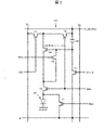
- FIG. 2 is a circuit diagram showing a pixel circuit of this embodiment.
- the pixel circuit PC the pixel capacitance Cp, the transistor T1 in which the gate electrode is connected to the scanning signal line GYn-2 in the previous stage (n-2 stages), and the scanning signal line in which the gate electrode is in its own stage (n stages).
- T2 setting transistor
- transistor T3 writing transistor
- transistor T4 transistor T4 that controls the current value of the light emitting element ED.
- the drive transistor the transistor T5 in which the gate electrode is connected to the light emission control signal line EMn of its own stage (n stage), the transistor T6 in which the gate electrode is connected to the light emission control signal line EMn, and the gate electrode is the light emission control signal. It includes an initialization transistor T7 connected to the line EMn.
- the gate electrode GE of the transistor T4 is connected to the power supply line PL via the pixel capacitance Cp and is connected to the initialization signal line IL via the transistor T1.
- a high voltage side power supply (EL VDD) is supplied to the power supply line PL, and a low voltage side power supply (ELVSS) is supplied to the cathode (upper electrode 25) of the initialization signal line IL and the light emitting element ED, for example.
- the source electrode of the transistor T4 is connected to the data signal line DLj via the transistor T3 and is connected to the power supply line PL via the transistor T5.
- the drain electrode of the transistor T4 is connected to the anode (lower electrode 22) of the light emitting element ED via the transistor T6, and is also connected to the gate electrode GE of the transistor T4 via the transistor T2.
- the anode of the light emitting device ED is connected to the initialization signal line IL via the transistor T7.
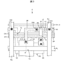
- FIG. 3 is a plan view showing the configuration of the TFT layer of the first embodiment.
- FIG. 4 is a cross-sectional view taken along the arrow of FIG.
- FIG. 5 is a timing chart showing the operation of the display device of the present embodiment.
- the TFT layer 4 includes a silicon film SFi / SHj formed on the barrier layer 3 and an inorganic insulating film 14 (first gate insulating film) covering the silicon film SFi / SFj.
- the first metal layer K1 formed above the inorganic insulating film 14 and including the scanning signal line GXn and the gate electrode GE of the transistor T4, the inorganic insulating film 16 covering the first metal layer K1, and the inorganic insulating film 16
- the second metal layer K2 formed on the upper layer and including the power supply line PL, the oxide semiconductor film ZF formed above the second metal layer K2, and the inorganic insulating film 18 (second) covering the oxide semiconductor film ZF.
- a fourth metal layer K4 formed above 20 and including a data signal line DLi / DLj and a source wiring JW, and a flattening film 21 covering the fourth metal layer K4 are provided.
- the silicon film SFi / SFj is composed of, for example, low temperature-formed polysilicon (LTPS).
- the silicon film SFi includes a conductor portion SD that functions as a conductor by being subjected to impurity doping or the like.
- the silicon film SFj includes a channel portion SC (superimposed portion with the first metal layer K1) that functions as a semiconductor, and a conductor portion SD that functions as a conductor by receiving an impurity doping or the like.
- the oxide semiconductor film ZF contains, for example, at least one element selected from indium (In), gallium (Ga), tin (Sn), hafnium (Hf), zirconium (Zr), and zinc (Zn) and oxygen. It is composed of a compound containing (for example, InGaZnO).
- the oxide semiconductor film ZF includes a channel portion (superimposed portion with the third metal layer K3) that functions as a semiconductor, and a conductor portion ZD that functions as a conductor.
- the first metal layer K1, the second metal layer K2, the third metal layer K3 and the fourth metal layer K4 include, for example, at least one of aluminum, tungsten, molybdenum, tantalum, chromium, titanium, and copper. It is composed of a layered film or a metal multi-layered film.
- the inorganic insulating film 14, 16, 18, and 20 may be composed of a single-layer film of silicon oxide (SiOx) or silicon nitride (SiNx), or may be composed of a laminated film thereof.
- the flattening film 21 can be made of a coatable organic material such as polyimide or acrylic resin.
- a signal corresponding to the video data (white gradation level in FIG. 5) is supplied to the vertical scanning period VT, and the video data is supplied to the update pause period PT.
- the data signal line DLi first data signal line
- the transistor T4 drive transistor
- the shield LE (relay electrode) that is electrically connected to the gate electrode GE of the above and the shield located between the data signal line DLi and the conductor LE in plan view and adjacent to each of the data signal line DLi and the conductor LE. Includes electrode A1.
- the conductor LE is included in the second metal layer K2, and the shield electrode is included in the first metal layer K1.
- the transistor T4 includes a channel portion SC (superimposed portion with the gate electrode GE) of the silicon film SFj, and a pixel capacitance Cp is formed between the gate electrode GE and the power supply line PL.
- the gate electrode GE is connected to the source wiring JW via the contact hole CH2, and the source wiring JW is connected to the conductor LE via the contact hole CH3. Further, the conductor portion ZD of the oxide semiconductor film ZF is provided so as to be in contact with the conductor LE.
- the first data signal line DLi and the conductor portion SD of the silicon film SFi are connected via the contact hole CH4 penetrating the inorganic insulating film 14, 16, 18, and 20, and in a plan view, the contact hole CH4 and the conductor LE.
- the shield electrode A1 is located between them.
- a signal corresponding to the video data (white gradation level in FIG. 5) is supplied to the vertical scanning period VT, and a constant potential signal not corresponding to the video data (additional voltage level in FIG. 5) is supplied to the update pause period PT.
- Data signal line DLj (second data signal line) to which Setting transistor) and included.
- the source electrode of the transistor T4 (conductor portion SD of the silicon film SFj) is connected to the second data signal line DLj via the transistor T3.
- the gate electrode GE of the transistor T4 is connected to the drain electrode of the transistor T4 (conductor portion SD of the silicon film SFj) via the transistor T2.
- the scanning signal line GXn is selected for the vertical scanning period VT and the update pause period PT (becomes active Low), and the scanning signal line GYn is selected for the vertical scanning period VT (active High). On the other hand, it is not selected for the renewal suspension period PT.
- the light emission control signal line EMn is in the active high (light-off state) during the period when at least one of the scanning signal lines GXn and GYn is selected.
- the length of the vertical scan period VT and the update pause period PT is, for example, 1/60 [second].
- the shield electrode A1 extending from the scanning signal line GXn suppresses the electric field formation (capacitive coupling) between the data signal line DLi and the conductor LE. Therefore, at the switching timing between the vertical scanning period VT and the update pause period PT (for example, the timing at which the potential of the data signal line DLi shifts from the white gradation level to the applied voltage level), the conductor LE (and the gate electrode GE) The potential is less likely to fluctuate. As a result, as shown in FIG. 5, the luminance difference between the refresh frame period RT and the non-refresh frame period NT in the sub-pixel SP is reduced. As a result, flicker (flickering of the screen) can be suppressed.
- the switching timing between the vertical scanning period VT and the update pause period PT (the timing at which the potential of the data signal line DLi shifts from the white gradation level to the applied voltage level). ) Raises the potential of the conductor LE (and the gate electrode GE). Therefore, in the sub-pixel SP, the luminance difference between the refresh frame period RT and the non-refresh frame period NT becomes large, and there is a possibility that low-frequency flicker may be visually recognized.
- the shield electrode A1 is included in the first metal layer K1, it is difficult to short-circuit both the data signal line DLi contained in the fourth metal layer K4 and the conductor LE included in the second metal layer K2.
- the constant potential signal (additional voltage level) in the update pause period PT may be a predetermined level from the white gradation level to the black gradation level.
- FIG. 5 shows a low frequency drive (refresh frequency 20 Hz) in which one update pause period PT follows one vertical scan period, which is an example and one update pause period PT after one vertical scan period. It may be a low frequency drive (refresh frequency is 30 Hz) followed by a low frequency drive (refresh frequency 10 Hz) in which one vertical scan period is followed by five update pause periods PT.
- FIG. 7 is a plan view showing the configuration of the TFT layer of the second embodiment.
- FIG. 8 is a cross-sectional view taken along the arrow of FIG. 7.
- the island-shaped electrode Q4 included in the fourth metal layer K4 and superimposing on the shield electrode A1 of the first metal layer K1 is provided, and the shield electrode A1 and the island-shaped electrode IE are provided with the inorganic insulating films 16 and 18. -Connected by a contact hole CHa penetrating 20. In this way, the electric field formation between the data signal line DLi and the conductor LE is suppressed more effectively.
- FIG. 9 is a plan view showing the configuration of the TFT layer of the third embodiment.
- FIG. 10 is a cross-sectional view taken along the arrow of FIG.
- the shield electrode A1 is extended from the scanning signal line GXn, but the present invention is not limited to this.
- From the scanning signal line GYn-2 scanning signal line controlling the transistor T1 in the own stage and the transistor T2 in the previous stage, see FIG. 2) included in the third metal layer K3 as in the third embodiment, in a plan view.
- a shield electrode A3 extending between the data signal line DLi and the conductor LE may be provided.
- the shield electrode A3 is included in the third metal layer K3, it is difficult to short-circuit both the data signal line DLi contained in the fourth metal layer K4 and the conductor LE included in the second metal layer K2.
- the gate electrode of the drive transistor is included in the first metal layer
- the first data signal line is included in the fourth metal layer
- the first data signal line and the conductor portion of the silicon film are connected via a contact hole.
- the gate electrode includes a writing transistor connected to the second scanning signal line.
- the source electrode of the drive transistor is connected to the second data signal line via the write transistor.
- the first scanning signal line is included in the first metal layer,
- the display device according to, for example, the fifth aspect, wherein the shield electrode extends from the first scanning signal line.
- a third scanning signal line included in the third metal layer is provided.
- the display device according to, for example, the fifth aspect, wherein the shield electrode extends from the third scanning signal line.
- Display device Light emitting element K1 to K4 1st to 4th metal layers SFi / SFj Silicon film SD Silicon film conductor part ZF Oxide semiconductor film ZD Oxide semiconductor film conductor part T2 setting Transistor T3 Write Transistor T4 Drive Transistor GE (Drive Transistor) Gate Electrode LE Conductor A1 Shield Electrode A3 Shield Electrode Cp Pixel Capacity DLi Data Signal Line (1st Data Signal Line) DLj data signal line (second data signal line) GXn scanning signal line (first scanning signal line) GYn scanning signal line (second scanning signal line) GYn-2 scanning signal line (third scanning signal line)
Landscapes
- Engineering & Computer Science (AREA)
- Microelectronics & Electronic Packaging (AREA)
- Physics & Mathematics (AREA)
- General Physics & Mathematics (AREA)
- Theoretical Computer Science (AREA)
- Computer Hardware Design (AREA)
- Geometry (AREA)
- Electroluminescent Light Sources (AREA)
- Devices For Indicating Variable Information By Combining Individual Elements (AREA)
- Control Of Indicators Other Than Cathode Ray Tubes (AREA)
Abstract
La présente invention comprend : une première ligne de signal de données (DLi) qui fournit un signal correspondant à des données vidéo dans une période de balayage vertical et qui fournit un signal qui ne correspond pas à des données vidéo dans une période d'interruption de mise à jour ; un transistor d'attaque (T4) qui commande la valeur de courant d'un élément électroluminescent ; un conducteur (LE) qui est électriquement connecté à une électrode de grille (GE) du transistor d'attaque ; et une électrode de blindage (A1) qui est positionnée, dans une vue en plan, entre la première ligne de signal de données (DLi) et le conducteur (LE) et qui est adjacente à la première ligne de signal de données et au conducteur.
Priority Applications (2)
| Application Number | Priority Date | Filing Date | Title |
|---|---|---|---|
| PCT/JP2020/046314 WO2022123776A1 (fr) | 2020-12-11 | 2020-12-11 | Dispositif d'affichage |
| US18/266,275 US20240049527A1 (en) | 2020-12-11 | 2020-12-11 | Display device |
Applications Claiming Priority (1)
| Application Number | Priority Date | Filing Date | Title |
|---|---|---|---|
| PCT/JP2020/046314 WO2022123776A1 (fr) | 2020-12-11 | 2020-12-11 | Dispositif d'affichage |
Publications (1)
| Publication Number | Publication Date |
|---|---|
| WO2022123776A1 true WO2022123776A1 (fr) | 2022-06-16 |
Family
ID=81974280
Family Applications (1)
| Application Number | Title | Priority Date | Filing Date |
|---|---|---|---|
| PCT/JP2020/046314 WO2022123776A1 (fr) | 2020-12-11 | 2020-12-11 | Dispositif d'affichage |
Country Status (2)
| Country | Link |
|---|---|
| US (1) | US20240049527A1 (fr) |
| WO (1) | WO2022123776A1 (fr) |
Cited By (1)
| Publication number | Priority date | Publication date | Assignee | Title |
|---|---|---|---|---|
| WO2024000701A1 (fr) * | 2022-06-29 | 2024-01-04 | 武汉华星光电半导体显示技术有限公司 | Circuit de pixel et écran d'affichage |
Citations (7)
| Publication number | Priority date | Publication date | Assignee | Title |
|---|---|---|---|---|
| JP2003271076A (ja) * | 2002-03-19 | 2003-09-25 | Toshiba Corp | 表示装置 |
| JP2009168898A (ja) * | 2008-01-11 | 2009-07-30 | Sony Corp | 自発光型表示装置 |
| WO2011048838A1 (fr) * | 2009-10-20 | 2011-04-28 | シャープ株式会社 | Substrat à matrice active et dispositif d'affichage el organique |
| JP2011146620A (ja) * | 2010-01-18 | 2011-07-28 | Seiko Epson Corp | 表示装置及び電子機器 |
| JP2013238724A (ja) * | 2012-05-15 | 2013-11-28 | Seiko Epson Corp | 電気光学装置および電子機器 |
| JP2018136565A (ja) * | 2018-04-11 | 2018-08-30 | セイコーエプソン株式会社 | 電気光学装置および電子機器 |
| US20200027939A1 (en) * | 2018-07-17 | 2020-01-23 | Samsung Display Co., Ltd. | Pixel and organic light emitting display device including the same |
-
2020
- 2020-12-11 US US18/266,275 patent/US20240049527A1/en active Pending
- 2020-12-11 WO PCT/JP2020/046314 patent/WO2022123776A1/fr active Application Filing
Patent Citations (7)
| Publication number | Priority date | Publication date | Assignee | Title |
|---|---|---|---|---|
| JP2003271076A (ja) * | 2002-03-19 | 2003-09-25 | Toshiba Corp | 表示装置 |
| JP2009168898A (ja) * | 2008-01-11 | 2009-07-30 | Sony Corp | 自発光型表示装置 |
| WO2011048838A1 (fr) * | 2009-10-20 | 2011-04-28 | シャープ株式会社 | Substrat à matrice active et dispositif d'affichage el organique |
| JP2011146620A (ja) * | 2010-01-18 | 2011-07-28 | Seiko Epson Corp | 表示装置及び電子機器 |
| JP2013238724A (ja) * | 2012-05-15 | 2013-11-28 | Seiko Epson Corp | 電気光学装置および電子機器 |
| JP2018136565A (ja) * | 2018-04-11 | 2018-08-30 | セイコーエプソン株式会社 | 電気光学装置および電子機器 |
| US20200027939A1 (en) * | 2018-07-17 | 2020-01-23 | Samsung Display Co., Ltd. | Pixel and organic light emitting display device including the same |
Cited By (1)
| Publication number | Priority date | Publication date | Assignee | Title |
|---|---|---|---|---|
| WO2024000701A1 (fr) * | 2022-06-29 | 2024-01-04 | 武汉华星光电半导体显示技术有限公司 | Circuit de pixel et écran d'affichage |
Also Published As
| Publication number | Publication date |
|---|---|
| US20240049527A1 (en) | 2024-02-08 |
Similar Documents
| Publication | Publication Date | Title |
|---|---|---|
| US20240021162A1 (en) | Organic light-emitting diode (oled) display and method of manufacturing the same | |
| JP4044014B2 (ja) | アクティブマトリクス型有機電界発光素子用薄膜トランジスタ | |
| US10950678B2 (en) | Thin film transistor substrate and organic light-emitting display using the same | |
| JP6397654B2 (ja) | 有機el発光装置 | |
| JP6906363B2 (ja) | 表示装置 | |
| WO2019187159A1 (fr) | Dispositif d'affichage | |
| KR102268493B1 (ko) | 유기발광다이오드 표시장치 및 이의 제조방법 | |
| EP3712950A1 (fr) | Dispositif d'affichage à diode électroluminescente organique comprenant un câble d'alimentation | |
| KR20170080963A (ko) | 유기발광 표시패널 및 이를 포함하는 유기발광 표시장치 | |
| JP2020109452A (ja) | 表示装置及び表示装置の製造方法 | |
| KR102607376B1 (ko) | 유기 발광 표시 장치 | |
| JP2021108366A (ja) | 薄膜デバイス | |
| JP2018088354A (ja) | 有機el表示装置 | |
| JP7478521B2 (ja) | 有機el表示装置 | |
| WO2022123776A1 (fr) | Dispositif d'affichage | |
| WO2020217478A1 (fr) | Dispositif d'affichage | |
| US20220028963A1 (en) | Organic light emitting display device | |
| JP2019003040A (ja) | 表示装置 | |
| JP2015176800A (ja) | 発光表示装置 | |
| WO2019187156A1 (fr) | Dispositif d'affichage | |
| US11018160B2 (en) | Thin-film transistor substrate and luminescent device | |
| JP5212683B2 (ja) | トランジスタパネル及びその製造方法 | |
| JP6962773B2 (ja) | 表示装置 | |
| WO2019187074A1 (fr) | Dispositif d'affichage | |
| WO2021240584A1 (fr) | Dispositif d'affichage et procédé de production de dispositif d'affichage |
Legal Events
| Date | Code | Title | Description |
|---|---|---|---|
| 121 | Ep: the epo has been informed by wipo that ep was designated in this application |
Ref document number: 20965158 Country of ref document: EP Kind code of ref document: A1 |
|
| WWE | Wipo information: entry into national phase |
Ref document number: 18266275 Country of ref document: US |
|
| NENP | Non-entry into the national phase |
Ref country code: DE |
|
| 122 | Ep: pct application non-entry in european phase |
Ref document number: 20965158 Country of ref document: EP Kind code of ref document: A1 |
|
| NENP | Non-entry into the national phase |
Ref country code: JP |