WO2022118802A1 - セラミック焼結体及び半導体装置用基板 - Google Patents
セラミック焼結体及び半導体装置用基板 Download PDFInfo
- Publication number
- WO2022118802A1 WO2022118802A1 PCT/JP2021/043716 JP2021043716W WO2022118802A1 WO 2022118802 A1 WO2022118802 A1 WO 2022118802A1 JP 2021043716 W JP2021043716 W JP 2021043716W WO 2022118802 A1 WO2022118802 A1 WO 2022118802A1
- Authority
- WO
- WIPO (PCT)
- Prior art keywords
- sintered body
- ceramic sintered
- mass
- content
- layer portion
- Prior art date
- Legal status (The legal status is an assumption and is not a legal conclusion. Google has not performed a legal analysis and makes no representation as to the accuracy of the status listed.)
- Ceased
Links
Images


Classifications
-
- H—ELECTRICITY
- H05—ELECTRIC TECHNIQUES NOT OTHERWISE PROVIDED FOR
- H05K—PRINTED CIRCUITS; CASINGS OR CONSTRUCTIONAL DETAILS OF ELECTRIC APPARATUS; MANUFACTURE OF ASSEMBLAGES OF ELECTRICAL COMPONENTS
- H05K1/00—Printed circuits
- H05K1/02—Details
- H05K1/03—Use of materials for the substrate
- H05K1/0306—Inorganic insulating substrates, e.g. ceramic, glass
-
- C—CHEMISTRY; METALLURGY
- C04—CEMENTS; CONCRETE; ARTIFICIAL STONE; CERAMICS; REFRACTORIES
- C04B—LIME, MAGNESIA; SLAG; CEMENTS; COMPOSITIONS THEREOF, e.g. MORTARS, CONCRETE OR LIKE BUILDING MATERIALS; ARTIFICIAL STONE; CERAMICS; REFRACTORIES; TREATMENT OF NATURAL STONE
- C04B35/00—Shaped ceramic products characterised by their composition; Ceramics compositions; Processing powders of inorganic compounds preparatory to the manufacturing of ceramic products
- C04B35/01—Shaped ceramic products characterised by their composition; Ceramics compositions; Processing powders of inorganic compounds preparatory to the manufacturing of ceramic products based on oxide ceramics
- C04B35/10—Shaped ceramic products characterised by their composition; Ceramics compositions; Processing powders of inorganic compounds preparatory to the manufacturing of ceramic products based on oxide ceramics based on aluminium oxide
- C04B35/111—Fine ceramics
- C04B35/117—Composites
- C04B35/119—Composites with zirconium oxide
-
- C—CHEMISTRY; METALLURGY
- C04—CEMENTS; CONCRETE; ARTIFICIAL STONE; CERAMICS; REFRACTORIES
- C04B—LIME, MAGNESIA; SLAG; CEMENTS; COMPOSITIONS THEREOF, e.g. MORTARS, CONCRETE OR LIKE BUILDING MATERIALS; ARTIFICIAL STONE; CERAMICS; REFRACTORIES; TREATMENT OF NATURAL STONE
- C04B35/00—Shaped ceramic products characterised by their composition; Ceramics compositions; Processing powders of inorganic compounds preparatory to the manufacturing of ceramic products
- C04B35/622—Forming processes; Processing powders of inorganic compounds preparatory to the manufacturing of ceramic products
- C04B35/626—Preparing or treating the powders individually or as batches ; preparing or treating macroscopic reinforcing agents for ceramic products, e.g. fibres; mechanical aspects section B
- C04B35/62605—Treating the starting powders individually or as mixtures
- C04B35/62625—Wet mixtures
- C04B35/6264—Mixing media, e.g. organic solvents
-
- C—CHEMISTRY; METALLURGY
- C04—CEMENTS; CONCRETE; ARTIFICIAL STONE; CERAMICS; REFRACTORIES
- C04B—LIME, MAGNESIA; SLAG; CEMENTS; COMPOSITIONS THEREOF, e.g. MORTARS, CONCRETE OR LIKE BUILDING MATERIALS; ARTIFICIAL STONE; CERAMICS; REFRACTORIES; TREATMENT OF NATURAL STONE
- C04B35/00—Shaped ceramic products characterised by their composition; Ceramics compositions; Processing powders of inorganic compounds preparatory to the manufacturing of ceramic products
- C04B35/622—Forming processes; Processing powders of inorganic compounds preparatory to the manufacturing of ceramic products
- C04B35/626—Preparing or treating the powders individually or as batches ; preparing or treating macroscopic reinforcing agents for ceramic products, e.g. fibres; mechanical aspects section B
- C04B35/63—Preparing or treating the powders individually or as batches ; preparing or treating macroscopic reinforcing agents for ceramic products, e.g. fibres; mechanical aspects section B using additives specially adapted for forming the products, e.g.. binder binders
- C04B35/632—Organic additives
- C04B35/634—Polymers
- C04B35/63404—Polymers obtained by reactions only involving carbon-to-carbon unsaturated bonds
- C04B35/6342—Polyvinylacetals, e.g. polyvinylbutyral [PVB]
-
- C—CHEMISTRY; METALLURGY
- C04—CEMENTS; CONCRETE; ARTIFICIAL STONE; CERAMICS; REFRACTORIES
- C04B—LIME, MAGNESIA; SLAG; CEMENTS; COMPOSITIONS THEREOF, e.g. MORTARS, CONCRETE OR LIKE BUILDING MATERIALS; ARTIFICIAL STONE; CERAMICS; REFRACTORIES; TREATMENT OF NATURAL STONE
- C04B37/00—Joining burned ceramic articles with other burned ceramic articles or other articles by heating
- C04B37/02—Joining burned ceramic articles with other burned ceramic articles or other articles by heating with metallic articles
- C04B37/021—Joining burned ceramic articles with other burned ceramic articles or other articles by heating with metallic articles in a direct manner, e.g. direct copper bonding [DCB]
-
- H—ELECTRICITY
- H05—ELECTRIC TECHNIQUES NOT OTHERWISE PROVIDED FOR
- H05K—PRINTED CIRCUITS; CASINGS OR CONSTRUCTIONAL DETAILS OF ELECTRIC APPARATUS; MANUFACTURE OF ASSEMBLAGES OF ELECTRICAL COMPONENTS
- H05K3/00—Apparatus or processes for manufacturing printed circuits
- H05K3/38—Improvement of the adhesion between the insulating substrate and the metal
-
- C—CHEMISTRY; METALLURGY
- C04—CEMENTS; CONCRETE; ARTIFICIAL STONE; CERAMICS; REFRACTORIES
- C04B—LIME, MAGNESIA; SLAG; CEMENTS; COMPOSITIONS THEREOF, e.g. MORTARS, CONCRETE OR LIKE BUILDING MATERIALS; ARTIFICIAL STONE; CERAMICS; REFRACTORIES; TREATMENT OF NATURAL STONE
- C04B2235/00—Aspects relating to ceramic starting mixtures or sintered ceramic products
- C04B2235/02—Composition of constituents of the starting material or of secondary phases of the final product
- C04B2235/30—Constituents and secondary phases not being of a fibrous nature
- C04B2235/36—Glass starting materials for making ceramics, e.g. silica glass
-
- C—CHEMISTRY; METALLURGY
- C04—CEMENTS; CONCRETE; ARTIFICIAL STONE; CERAMICS; REFRACTORIES
- C04B—LIME, MAGNESIA; SLAG; CEMENTS; COMPOSITIONS THEREOF, e.g. MORTARS, CONCRETE OR LIKE BUILDING MATERIALS; ARTIFICIAL STONE; CERAMICS; REFRACTORIES; TREATMENT OF NATURAL STONE
- C04B2235/00—Aspects relating to ceramic starting mixtures or sintered ceramic products
- C04B2235/60—Aspects relating to the preparation, properties or mechanical treatment of green bodies or pre-forms
- C04B2235/602—Making the green bodies or pre-forms by moulding
- C04B2235/6025—Tape casting, e.g. with a doctor blade
-
- C—CHEMISTRY; METALLURGY
- C04—CEMENTS; CONCRETE; ARTIFICIAL STONE; CERAMICS; REFRACTORIES
- C04B—LIME, MAGNESIA; SLAG; CEMENTS; COMPOSITIONS THEREOF, e.g. MORTARS, CONCRETE OR LIKE BUILDING MATERIALS; ARTIFICIAL STONE; CERAMICS; REFRACTORIES; TREATMENT OF NATURAL STONE
- C04B2235/00—Aspects relating to ceramic starting mixtures or sintered ceramic products
- C04B2235/65—Aspects relating to heat treatments of ceramic bodies such as green ceramics or pre-sintered ceramics, e.g. burning, sintering or melting processes
- C04B2235/656—Aspects relating to heat treatments of ceramic bodies such as green ceramics or pre-sintered ceramics, e.g. burning, sintering or melting processes characterised by specific heating conditions during heat treatment
- C04B2235/6567—Treatment time
-
- C—CHEMISTRY; METALLURGY
- C04—CEMENTS; CONCRETE; ARTIFICIAL STONE; CERAMICS; REFRACTORIES
- C04B—LIME, MAGNESIA; SLAG; CEMENTS; COMPOSITIONS THEREOF, e.g. MORTARS, CONCRETE OR LIKE BUILDING MATERIALS; ARTIFICIAL STONE; CERAMICS; REFRACTORIES; TREATMENT OF NATURAL STONE
- C04B2235/00—Aspects relating to ceramic starting mixtures or sintered ceramic products
- C04B2235/70—Aspects relating to sintered or melt-casted ceramic products
- C04B2235/72—Products characterised by the absence or the low content of specific components, e.g. alkali metal free alumina ceramics
-
- C—CHEMISTRY; METALLURGY
- C04—CEMENTS; CONCRETE; ARTIFICIAL STONE; CERAMICS; REFRACTORIES
- C04B—LIME, MAGNESIA; SLAG; CEMENTS; COMPOSITIONS THEREOF, e.g. MORTARS, CONCRETE OR LIKE BUILDING MATERIALS; ARTIFICIAL STONE; CERAMICS; REFRACTORIES; TREATMENT OF NATURAL STONE
- C04B2235/00—Aspects relating to ceramic starting mixtures or sintered ceramic products
- C04B2235/70—Aspects relating to sintered or melt-casted ceramic products
- C04B2235/95—Products characterised by their size, e.g. microceramics
-
- C—CHEMISTRY; METALLURGY
- C04—CEMENTS; CONCRETE; ARTIFICIAL STONE; CERAMICS; REFRACTORIES
- C04B—LIME, MAGNESIA; SLAG; CEMENTS; COMPOSITIONS THEREOF, e.g. MORTARS, CONCRETE OR LIKE BUILDING MATERIALS; ARTIFICIAL STONE; CERAMICS; REFRACTORIES; TREATMENT OF NATURAL STONE
- C04B2235/00—Aspects relating to ceramic starting mixtures or sintered ceramic products
- C04B2235/70—Aspects relating to sintered or melt-casted ceramic products
- C04B2235/96—Properties of ceramic products, e.g. mechanical properties such as strength, toughness, wear resistance
-
- C—CHEMISTRY; METALLURGY
- C04—CEMENTS; CONCRETE; ARTIFICIAL STONE; CERAMICS; REFRACTORIES
- C04B—LIME, MAGNESIA; SLAG; CEMENTS; COMPOSITIONS THEREOF, e.g. MORTARS, CONCRETE OR LIKE BUILDING MATERIALS; ARTIFICIAL STONE; CERAMICS; REFRACTORIES; TREATMENT OF NATURAL STONE
- C04B2237/00—Aspects relating to ceramic laminates or to joining of ceramic articles with other articles by heating
- C04B2237/30—Composition of layers of ceramic laminates or of ceramic or metallic articles to be joined by heating, e.g. Si substrates
- C04B2237/32—Ceramic
- C04B2237/34—Oxidic
- C04B2237/343—Alumina or aluminates
-
- H—ELECTRICITY
- H10—SEMICONDUCTOR DEVICES; ELECTRIC SOLID-STATE DEVICES NOT OTHERWISE PROVIDED FOR
- H10W—GENERIC PACKAGES, INTERCONNECTIONS, CONNECTORS OR OTHER CONSTRUCTIONAL DETAILS OF DEVICES COVERED BY CLASS H10
- H10W40/00—Arrangements for thermal protection or thermal control
- H10W40/10—Arrangements for heating
-
- H—ELECTRICITY
- H10—SEMICONDUCTOR DEVICES; ELECTRIC SOLID-STATE DEVICES NOT OTHERWISE PROVIDED FOR
- H10W—GENERIC PACKAGES, INTERCONNECTIONS, CONNECTORS OR OTHER CONSTRUCTIONAL DETAILS OF DEVICES COVERED BY CLASS H10
- H10W40/00—Arrangements for thermal protection or thermal control
- H10W40/20—Arrangements for cooling
- H10W40/25—Arrangements for cooling characterised by their materials
- H10W40/255—Arrangements for cooling characterised by their materials having a laminate or multilayered structure, e.g. direct bond copper [DBC] ceramic substrates
-
- H—ELECTRICITY
- H10—SEMICONDUCTOR DEVICES; ELECTRIC SOLID-STATE DEVICES NOT OTHERWISE PROVIDED FOR
- H10W—GENERIC PACKAGES, INTERCONNECTIONS, CONNECTORS OR OTHER CONSTRUCTIONAL DETAILS OF DEVICES COVERED BY CLASS H10
- H10W70/00—Package substrates; Interposers; Redistribution layers [RDL]
- H10W70/60—Insulating or insulated package substrates; Interposers; Redistribution layers
- H10W70/62—Insulating or insulated package substrates; Interposers; Redistribution layers characterised by their interconnections
- H10W70/66—Conductive materials thereof
-
- H—ELECTRICITY
- H10—SEMICONDUCTOR DEVICES; ELECTRIC SOLID-STATE DEVICES NOT OTHERWISE PROVIDED FOR
- H10W—GENERIC PACKAGES, INTERCONNECTIONS, CONNECTORS OR OTHER CONSTRUCTIONAL DETAILS OF DEVICES COVERED BY CLASS H10
- H10W70/00—Package substrates; Interposers; Redistribution layers [RDL]
- H10W70/60—Insulating or insulated package substrates; Interposers; Redistribution layers
- H10W70/67—Insulating or insulated package substrates; Interposers; Redistribution layers characterised by their insulating layers or insulating parts
- H10W70/69—Insulating materials thereof
- H10W70/692—Ceramics or glasses
Definitions
- the present invention relates to a ceramic sintered body and a substrate for a semiconductor device.
- a DBOC substrate Direct Bonding of Copper Substrate having a copper plate on the surface of a ceramic sintered body is known (for example, Patent Document 1).
- a copper plate is bonded to the surface of the ceramic sintered body, but the present inventor has found that when the oxygen ion conductivity of the ceramic sintered body becomes high, the ceramic is ceramic when a DC voltage is applied. It has been found that the bonding strength between the sintered body and the copper plate is lowered, and the copper plate may be peeled off.
- the present invention has been made to solve the above problems, and when a copper plate is joined, it can suppress peeling when a DC voltage is applied, and is a substrate for a ceramic sintered body and a semiconductor device.
- the purpose is to provide.
- the ceramic sintered body according to the present invention contains alumina, zirconia, yttria, a glass component containing silica and magnesia, and has a bonding layer portion having a magnesium concentration peak on the surface side, and the bonding layer portion.
- An inner layer portion having a magnesium concentration peak smaller than that of the bond layer portion is provided on the inner side adjacent to the inner layer portion.
- the inner layer portion has at least a first region adjacent to the inner side of the bonding layer portion and a second region adjacent to the inner side of the first region, and the first region.
- the concentration peak of magnesium in the two regions can be smaller than the concentration peak in the bonding layer portion and larger than the concentration peak in the first region.
- the content of the zirconia can be 10% by mass or more and 25% by mass or less.
- the content of the zirconia when the content of the zirconia is 10% by mass or more and 15% by mass or less, the content of the silica may be 0.7% by mass or more and 1.5% by mass or less. can.
- the content of the zirconia when the content of the zirconia is higher than 15% by mass and 25% by mass or less, the content of the silica is 1.5% by mass or more and 2.0% by mass or less. Can be done.
- the content of the magnesia can be 0.1% by mass or more and 0.8% by mass or less.
- the semiconductor device substrate according to the present invention is a semiconductor device substrate for mounting electronic components, and includes the ceramic sintered body according to any one of the above, a copper plate bonded to the ceramic sintered body, and the like. It is equipped with.
- FIG. 1 It is sectional drawing which shows one Embodiment of the semiconductor device which has the substrate for the semiconductor device which concerns on this invention. It is a graph which shows the relationship between the frequency and impedance of the comparative example 1. FIG. It is a graph which shows the relationship between the frequency and impedance of Example 1.
- FIG. It is a figure which shows the elemental distribution of silicon (Si) near the surface of the comparative example 1.
- FIG. It is a figure which shows the elemental distribution of silicon (Si) near the surface of Example 1.
- Mg elemental distribution of magnesium
- FIG. 1 is a cross-sectional view of a semiconductor device having a semiconductor device substrate according to the present embodiment.
- the semiconductor device includes, for example, an automobile, an air conditioner, an industrial robot, a commercial elevator, a household microwave oven, an IH electric rice cooker, power generation (wind power generation, solar power generation, fuel cell, etc.), electric railway, and the like. It is used as a power module in various electronic devices such as UPS (non-disruptive power source).
- UPS non-disruptive power source
- the semiconductor device 1 includes a semiconductor device substrate 2, a first bonding material 5, a second bonding material 5', a semiconductor chip 6, a bonding wire 7, and a heat sink 8. There is.
- the substrate 2 for a semiconductor device is a so-called DBOC substrate (Direct Bonding of Copper Substrate), which is a plate-shaped ceramic sintered body 3 which is an insulator, and a first copper plate 4 bonded to one surface (upper surface) thereof. , A second copper plate 4'joined to the other surface (lower surface). Details of the ceramic sintered body 3 will be described later.
- DBOC substrate Direct Bonding of Copper Substrate
- a transmission circuit is formed on the first copper plate 4.
- the second copper plate 4' is formed in a flat plate shape.
- the semiconductor chip 6 is bonded to the upper surface of the semiconductor device substrate 2, that is, a part of the upper surface of the first copper plate 4, via the first bonding material 5. Further, the semiconductor chip 6 and the first copper plate 4 are connected by the bonding wire 7.
- the heat sink 8 is bonded to the lower surface of the semiconductor device substrate 2, that is, the lower surface of the second copper plate 4'via the second bonding material 5'.
- the heat sink 8 is known and can be made of a metal such as copper.
- the transmission circuit formed on the first copper plate 4 can be formed by, for example, a subtractive method or an additive method.
- the ceramic sintered body 3 contains alumina (Al 2 O 3 ), zirconia (ZrO 2 ), ytria (Y 2 O 3 ), a glass component, and the rest other than these.
- the glass component contains silica (SiO 2 ) and magnesia (MgO).
- SiO 2 silica
- MgO magnesia
- the content of alumina is preferably, for example, 75% by mass or more and 90% by mass or less, and more preferably 85% by mass or more and 90% by mass or less.
- the content of zirconia is preferably 10% by mass or more and 25% by mass or less, and more preferably 10% by mass or more and 15% by mass or less.
- the strength of the ceramic sintered body 3 can be improved.
- the linear thermal expansion coefficient of the ceramic sintered body 3 can be suppressed from becoming too small, and the difference in the linear thermal expansion coefficient between the ceramic sintered body 3 and the first and second copper plates 4, 4'can be reduced. ..
- the thermal stress generated at the joining interface can be reduced, which contributes to suppressing the occurrence of cracks in the ceramic sintered body 3 at the joining interface.
- the content of zirconia it is considered that by setting the content of zirconia to 25% by mass or less, it is possible to suppress an excessive reaction at the bonding interface at the time of copper plate bonding, and it is possible to suppress the formation of voids at the bonding interface. This is because the wettability of alumina and the Cu—O eutectic liquid phase at the time of joining the copper plate of zirconia is different. Further, by setting the zirconia content to 25% by mass or less, the impedance of the ceramic sintered body 3 can be improved without increasing the silica content, as will be described later.
- the content of itria is preferably 0.8% by mass or more and 1.9% by mass or less.
- the content is considered that the proportion of the monoclinic phase in the zirconia crystal phase can be suppressed from becoming excessive, while the proportion of the tetragonal phase can be increased.
- the mechanical strength of the ceramic sintered body 3 can be improved, which contributes to suppressing the occurrence of cracks in the ceramic sintered body 3 at the joining interface.
- the ratio of the content of yttrium to the content of zirconia is preferably 4.5% by mass or more and 7.9% by mass or less.
- the silica content is preferably 0.1% by mass or more and 2.5% by mass or less.
- the silica content is 0.1% by mass or more, the oxygen ion conductivity of the ceramic sintered body 3 is suppressed and the impedance can be improved, as will be described later.
- the silica content is high, the strength of the ceramic sintered body 3 may decrease, but in order to suppress this, the silica content is preferably 2.5% by mass or less.
- the content of zirconia when the content of zirconia is 10% by mass or more and 15% by mass or less, the content of silica is preferably 0.7% by mass or more and 1.5% by mass or less. When the content of zirconia is higher than 15% by mass and 25% by mass or less, the content of silica is preferably 1.5% by mass or more and 2.0% by mass or less. As described above, the impedance of the ceramic sintered body 3 can be effectively improved by changing the silica content according to the zirconia content.
- the content of magnesia is preferably 0.1% by mass or more and 0.8% by mass or less, and more preferably 0.15% by mass or more and 0.3% by mass or less.
- the ceramic sintered body 3 can be sintered without excessively increasing the firing temperature, and the coarsening of alumina particles and zirconia particles can be suppressed. Conceivable. As a result, it is considered that the mechanical strength of the ceramic sintered body 3 can be improved, which contributes to suppressing the occurrence of cracks in the ceramic sintered body 3 at the joining interface.
- spinel crystals MgAl 2 O 4 crystals
- the glass component may contain calcia (CaO).
- calcia calcia
- the content of calcia is preferably 0.03% by mass or more and 0.35% by mass or less.
- the content of the balance is preferably 0.05% by mass or less in terms of oxide.
- the content of the constituent elements of the ceramic sintered body 3 is calculated in terms of oxide as described above, but the constituent elements of the ceramic sintered body 3 exist in the form of oxide. It may or may not be present in the form of an oxide.
- at least one of Y, Mg and Ca does not exist in the form of an oxide and may be dissolved in ZrO2.
- the content of the constituent elements of the ceramic sintered body 3 in terms of oxide is calculated as follows. First, the constituent elements of the ceramic sintered body 3 are qualitatively analyzed using an energy dispersive analyzer (EDS) attached to a fluorescent X-ray analyzer (XRF) or a scanning electron microscope (SEM). Next, each element detected by this qualitative analysis is quantitatively analyzed using an ICP emission spectrophotometer. Next, the content of each element measured by this quantitative analysis is converted into an oxide.
- EDS energy dispersive analyzer
- XRF fluorescent X-ray analyzer
- SEM scanning electron microscope
- XRF X-ray Fluorescence Analysis
- SEM Scanning Electron Microscope
- EDS Energy Dispersive X-ray Specrocstopy
- ICP Inductively abbreviated as Inductive Co.
- the element contained in the balance may be an element that is intentionally added or an element that is unavoidably mixed.
- the elements contained in the balance are not particularly limited, and examples thereof include Fe (iron), Ti (titanium), and Mn (manganese).
- an organic binder for example, polyvinyl butyral
- a solvent xylene, toluene, etc.
- a plasticizer dioctyl phthalate, etc.
- the slurry-like substance is molded into a desired shape by a desired molding means (for example, mold press, cold hydrostatic press, injection molding, doctor blade method, extrusion molding method, etc.) to form a ceramic molded body.
- a desired molding means for example, mold press, cold hydrostatic press, injection molding, doctor blade method, extrusion molding method, etc.
- the ceramic molded body is fired in an oxygen atmosphere or an air atmosphere (1560 ° C. to 1620 ° C., 0.7 hours to 1.0 hours) to complete the ceramic sintered body 3.
- a Cu—O—Al bond is formed at the interface between the first copper plate 4 and the second copper plate 4 ′ and the ceramic sintered body 3 in the process of forming and solidifying a Cu—O eutectic liquid phase.
- the second copper plate 4' is connected to the positive electrode, and a DC voltage is applied to them, in the vicinity of the interface between the first copper plate 4 and the ceramic sintered body 3.
- Cu—O—Al bond is reduced.
- the bonding strength between the first copper plate 4 and the ceramic sintered body 3 is reduced. Oxygen ions generated by this reduction move to the second copper plate 4'via the ceramic sintered body 3.
- the second copper plate 4' is oxidized by oxygen ions, and the bonding strength between the second copper plate 4'and the ceramic sintered body 3 is lowered.
- the movement of oxygen ions when such a DC voltage is applied will be referred to as behavior A.
- the present inventor has found that the movement of oxygen ions and electrons can be suppressed when silica is contained in the ceramic sintered body 3. That is, it has been found that when silica is contained in the ceramic sintered body 3, oxygen ions and electrons are trapped by the silica and the propagation of oxygen ions and electrons is suppressed. In this case, since the behavior A is suppressed, the first copper plate 4 and the second copper plate 4'are not peeled off due to the reduction of the Cu—O—Al bond even when a DC voltage is applied.
- the present inventor measured the degree of propagation of such oxygen ions and electrons as the impedance of the ceramic sintered body 3. That is, the lower the oxygen ion conductivity, the higher the impedance.
- silica is present inside the ceramic sintered body 3 as described above.
- magnesia is present at the bonding interface between the ceramic sintered body 3 and the first copper plate 4, a bond of Cu—O—Al—Mg occurs and oxygen is less likely to be reduced. Therefore, the behavior A when a DC voltage is applied is suppressed. Therefore, the peeling of the first copper plate 4 due to the reduction of oxygen can be suppressed.
- the glass component reduces the strength of the ceramic sintered body 3. Considering that cracks at the bonding interface proceed from the surface of the ceramic sintered body 3 to the inside, it is desirable that there is little glass component in the vicinity of the surface of the ceramic sintered body 3. Peeling of the first copper plate 4 also occurs due to cracks generated at the joint interface due to the difference in linear thermal expansion coefficient between the ceramic sintered body 3 and the first copper plate 4.
- the present inventor provides a bonding layer portion having a magnesium concentration peak at the bonding interface between the ceramic sintered body 3 and the first copper plate 4, so that the first copper plate 4 can be peeled off when a DC voltage is applied. I found that it can be suppressed. On the other hand, it was found that the peeling of the first copper plate 4 due to thermal stress can be suppressed by having an inner layer portion in which the magnesium concentration peak is smaller than that in the bond layer portion on the inner side (deep position) adjacent to the bond layer portion. rice field.
- the concentration of magnesium in the inner layer portion may be smaller than that in the binding layer portion, and may have various concentration peaks, and is not particularly limited. For example, the concentration of magnesium in the inner layer may be substantially constant.
- the inner layer portion is adjacent to the first region where the magnesium concentration is low on the inner side of the bond layer portion and the inner side of the first region, and the magnesium concentration peak is smaller than the concentration peak of the bond layer portion and is the first. It may include a second region having a concentration peak larger than one region.
- the ceramic sintered bodies according to Example 1 and Comparative Example 1 composed of the following materials as main components were prepared. Specifically, first, the powder material prepared with the compositions shown in Table 1A was pulverized and mixed by a ball mill. In Tables 1A and 1B, mass% is expressed as wt%. Further, Table 1B shows the conversion of the composition of Example 1 so that the total value is exactly 100 wt%. In Example 1, the amount of silica added was 1.11 wt%. On the other hand, in Comparative Example 1, the amount of silica added was substantially zero.
- polyvinyl butyral as an organic binder xylene as a solvent, and dioctyl phthalate as a plasticizer were added to the pulverized and mixed powder material to form a slurry-like substance.
- a ceramic molded body was produced by molding a slurry-like substance into a sheet by the doctor blade method.
- the ceramic molded product was fired at 1570 ° C. for 0.8 hours in an air atmosphere to prepare a ceramic sintered body.
- the size of the ceramic sintered body 3 was 0.32 mm in thickness, 39 mm in length, and 45 mm in width.
- the content of the constituent elements of the ceramic sintered body 3 in terms of oxide was measured by the method shown in paragraph 0038, it was almost the same as the mixing ratio of the powder material shown in Table 1.
- FIGS. 2A and 2B show the result of Comparative Example 1
- FIG. 2B shows the result of Example 1.
- E + 03 means 1 times 10 to the 3rd power.
- the measuring method is an AC impedance measuring method.
- the impedance was measured when an AC voltage of 1 Vrms was applied to the ceramic sintered body and when a DC voltage of 100 V was applied and then an AC voltage of 1 Vrms was further applied.
- the impedance at a low frequency is different between the case where only the AC voltage is applied (AC only) and the case where the AC voltage and the DC voltage are applied (AC + DC). .. Specifically, 1. E-03 ⁇ 1. In the frequency range of E-01 (Hz), the impedance is lower when the AC voltage and the DC voltage are applied (AC + DC) than when only the AC voltage is applied (AC only). This is an effect of the above-mentioned behavior A, and it is considered that the oxygen ion moves and the impedance is lowered because the behavior A occurs when the AC voltage and the DC voltage are applied.
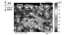
- FIGS. 3A and 3B show the elemental distribution of Si (silicon) in the cross section near the bonding interface between the copper plate and the ceramic sintered body according to Example 1 and Comparative Example 1.
- the results are as shown in FIGS. 3A and 3B.
- FIG. 3A shows the result of Comparative Example 1
- FIG. 3B shows the result of Example 1.
- the element distribution was measured by a field emission electron probe microanalyzer.
- FIGS. 4A and 4B show the result of Comparative Example 1
- FIG. 4B shows the result of Example 1.
- Mg is largely distributed near the surface layer of the ceramic sintered body, that is, near the bonding interface with the copper plate (see the white arrow).
- Mg is low on the inner side (deep position) adjacent to the junction interface. This region corresponds to the first region described later.
- the positions of the arrows in FIG. 3B and the white arrows in FIG. 4B are the same except for the vicinity of the joining interface. This indicates that a glass component containing silica and magnesia is formed inside the ceramic sintered body.
- 5A is a backscattered electron image at the same location as FIGS. 3B and 4B.
- a 20 ⁇ m ⁇ 20 ⁇ m area (square frame) including a copper plate and a ceramic sintered body was set. This area was divided into small areas of 256 ⁇ 256. One side of the small area is 0.078 ⁇ m, which is 20 ⁇ m divided by 256.
- the magnesium concentration in each small area was calculated. Then, the magnesium concentration (mass%) was averaged in 256 small areas in the horizontal direction (X direction) in the figure. This is called the X-direction average element concentration.
- FIG. 5B is a graph with the vertical direction (Y direction) of FIG. 5A, that is, the depth direction of the ceramic sintered body as the horizontal axis, and the average value of the magnesium concentration at each depth is dotted on the vertical axis.
- the average value of the magnesium concentration means the average element concentration in the X direction.
- the average values of copper and aluminum concentrations were also scored in the same manner. Specifically, the X-direction average element concentration of copper and aluminum was dotd in the same manner as magnesium.
- the horizontal axis of this graph has the origin at the upper left corner of the square frame in FIG. 5A inside the copper plate.
- the ceramic sintered body when the position of the horizontal axis corresponding to 1/2 of the maximum value of the mass% of copper (here, 3.6 ⁇ m) is taken as the center value, it is approximately ⁇ 1.0 ⁇ m from the center value.
- the range of is defined as the above-mentioned bonding layer portion.
- the concentration peak of magnesium is located in the bond layer portion.
- the bonded layer portion is essentially regarded as a range in the Y-axis direction in which the average element concentration in the X direction of copper decreases from a constant value to almost zero from the copper plate toward the ceramic sintered body.
- This range is almost the same as the range in the Y-axis direction in which the average element concentration in the X direction of aluminum increases from almost zero to a constant value.
- the values on the Y-axis are almost the same.
- the range of such a bonding layer portion is approximately ⁇ 1.0 ⁇ m from the center value in FIG. 5B, but is not limited to this range. That is, as described above, the range of the bonded layer portion is the range in which the X-direction average element concentration of copper changes rapidly, the range in which the magnesium concentration peak exists, and the amount of oxidation of the copper plate surface before bonding. It may vary depending on the bonding temperature, the composition of the ceramic sintered body, and the like.
- the inner layer portion has a first region adjacent to the inner side of the connecting layer portion and a second region adjacent to the inner side of the first region.
- the second region has a concentration peak in which the concentration of magnesium increases in the depth direction from the first region and then decreases to about the concentration of the first region.
- the magnitude of the concentration peak of magnesium in the second region is smaller than the concentration peak in the bonding layer portion.
- the first region had a thickness of about 3 ⁇ m and the second region had a thickness of about 6 ⁇ m. Further, in the region on the inner side of the second region, the magnesium concentration was lower than the concentration peak in the second region.
- magnesium is low in the first region on the inner side adjacent to the bond layer (the concentration peak is smaller than the concentration peak in the bond layer). Therefore, in this region, the glass component is smaller than that in the bonded layer portion, so that the mechanical strength of the ceramic sintered body is increased. Since the cracks in the ceramic sintered body progress from the surface to the inside, this first region can prevent the copper plate from peeling off due to thermal stress.
- a glass component containing silica and magnesia is formed inside the ceramic sintered body. Therefore, it is considered that the X-direction average element concentration of Si is also high in the second region of the inner layer portion. Therefore, when the first copper plate 4 is connected to the negative electrode, the second copper plate 4'is connected to the positive electrode, and then a DC voltage is applied to the ceramic sintered body 3, such a second region becomes the ceramic sintered body 3. It suppresses the movement of oxygen ions from the second copper plate 4 to the second copper plate 4'.
- the ceramic sintered body of Example 1 has higher reliability than that of Comparative Example 1. That is, the copper plate is less likely to peel off when a DC voltage is applied or thermal stress is generated.
- Example 1 it is presumed that such segregation of magnesium in Example 1 was caused by the fact that magnesium was easily diffused by the molten glass component when the copper plate and the ceramic sintered body were joined.
- the concentration peak of magnesium was smaller than the concentration peak of the bonding layer portion and larger than the concentration peak of the first region in the second region, but the copper plate before bonding was formed.
- the above-mentioned magnesium concentration peak was found in this second region.
- Example 1 The change in the concentration of the inner layer portion shown in FIG. 5B is an example, and when the inner layer portion has the first region and the second region as described above, the thickness of each region is not limited to the thickness described above. However, it has been confirmed that the first region and the second region exist in a region within about 15 ⁇ m from the surface of the ceramic sintered body. In addition, an inner layer portion that does not have a concentration peak as in the second region and has a concentration substantially the same as that in the first region has also been confirmed.
- FIG. 6 shows the relationship between the silica content and the impedance when the zirconia content is 10 wt%, 15 wt%, and 22 wt%, respectively.
- the amount of SiO 2 added (wt%) on the horizontal axis has the same meaning as the content of silica (wt%).
- the impedance becomes high. You can see that there is.
- the content of zirconia is higher than 15% by mass and 25% by mass or less, and the content of silica is 1.5% by mass or more and 2.0% by mass or less, the impedance is high. I understand.
- the increase in impedance when an AC voltage is applied means that the oxygen ion conductivity has decreased. Therefore, oxygen ion conductivity when a DC voltage is applied can also be suppressed.
- Substrate for semiconductor devices 3 Ceramic sintered body 4, 4'... Copper plate
Landscapes
- Engineering & Computer Science (AREA)
- Chemical & Material Sciences (AREA)
- Ceramic Engineering (AREA)
- Manufacturing & Machinery (AREA)
- Materials Engineering (AREA)
- Structural Engineering (AREA)
- Organic Chemistry (AREA)
- Inorganic Chemistry (AREA)
- Microelectronics & Electronic Packaging (AREA)
- Chemical Kinetics & Catalysis (AREA)
- Composite Materials (AREA)
- Ceramic Products (AREA)
- Cooling Or The Like Of Semiconductors Or Solid State Devices (AREA)
- Compositions Of Oxide Ceramics (AREA)
Priority Applications (3)
| Application Number | Priority Date | Filing Date | Title |
|---|---|---|---|
| CN202180006937.8A CN114867699B (zh) | 2020-12-04 | 2021-11-29 | 陶瓷烧结体以及半导体装置用基板 |
| DE112021000182.5T DE112021000182T5 (de) | 2020-12-04 | 2021-11-29 | Keramiksinterkörper und Substrat für eine Halbleitervorrichtung |
| JP2022529894A JP7251001B2 (ja) | 2020-12-04 | 2021-11-29 | セラミック焼結体及び半導体装置用基板 |
Applications Claiming Priority (2)
| Application Number | Priority Date | Filing Date | Title |
|---|---|---|---|
| JP2020201979 | 2020-12-04 | ||
| JP2020-201979 | 2020-12-04 |
Publications (1)
| Publication Number | Publication Date |
|---|---|
| WO2022118802A1 true WO2022118802A1 (ja) | 2022-06-09 |
Family
ID=81853930
Family Applications (1)
| Application Number | Title | Priority Date | Filing Date |
|---|---|---|---|
| PCT/JP2021/043716 Ceased WO2022118802A1 (ja) | 2020-12-04 | 2021-11-29 | セラミック焼結体及び半導体装置用基板 |
Country Status (4)
| Country | Link |
|---|---|
| JP (1) | JP7251001B2 (https=) |
| CN (1) | CN114867699B (https=) |
| DE (1) | DE112021000182T5 (https=) |
| WO (1) | WO2022118802A1 (https=) |
Cited By (2)
| Publication number | Priority date | Publication date | Assignee | Title |
|---|---|---|---|---|
| WO2024053619A1 (ja) * | 2022-09-05 | 2024-03-14 | Ngkエレクトロデバイス株式会社 | セラミック基板、及びこれを備えた半導体装置用基板 |
| JPWO2024069888A1 (https=) * | 2022-09-29 | 2024-04-04 |
Citations (5)
| Publication number | Priority date | Publication date | Assignee | Title |
|---|---|---|---|---|
| WO2010114126A1 (ja) * | 2009-04-03 | 2010-10-07 | 株式会社住友金属エレクトロデバイス | セラミックス焼結体およびそれを用いた半導体装置用基板 |
| WO2012060341A1 (ja) * | 2010-11-01 | 2012-05-10 | 株式会社住友金属エレクトロデバイス | 電子部品素子収納用パッケージ |
| WO2014103465A1 (ja) * | 2012-12-25 | 2014-07-03 | ニッコー株式会社 | アルミナ質基板及び半導体装置用基板 |
| WO2020115870A1 (ja) * | 2018-12-06 | 2020-06-11 | 日本碍子株式会社 | セラミックス焼結体及び半導体装置用基板 |
| WO2020115868A1 (ja) * | 2018-12-06 | 2020-06-11 | 日本碍子株式会社 | セラミックス焼結体及び半導体装置用基板 |
Family Cites Families (2)
| Publication number | Priority date | Publication date | Assignee | Title |
|---|---|---|---|---|
| JP2001144433A (ja) * | 1999-11-18 | 2001-05-25 | Denki Kagaku Kogyo Kk | セラミックス回路基板 |
| TWI629753B (zh) * | 2013-04-26 | 2018-07-11 | Ngk Insulators, Ltd. | 半導體用複合基板之操作基板 |
-
2021
- 2021-11-29 DE DE112021000182.5T patent/DE112021000182T5/de active Pending
- 2021-11-29 CN CN202180006937.8A patent/CN114867699B/zh active Active
- 2021-11-29 JP JP2022529894A patent/JP7251001B2/ja active Active
- 2021-11-29 WO PCT/JP2021/043716 patent/WO2022118802A1/ja not_active Ceased
Patent Citations (5)
| Publication number | Priority date | Publication date | Assignee | Title |
|---|---|---|---|---|
| WO2010114126A1 (ja) * | 2009-04-03 | 2010-10-07 | 株式会社住友金属エレクトロデバイス | セラミックス焼結体およびそれを用いた半導体装置用基板 |
| WO2012060341A1 (ja) * | 2010-11-01 | 2012-05-10 | 株式会社住友金属エレクトロデバイス | 電子部品素子収納用パッケージ |
| WO2014103465A1 (ja) * | 2012-12-25 | 2014-07-03 | ニッコー株式会社 | アルミナ質基板及び半導体装置用基板 |
| WO2020115870A1 (ja) * | 2018-12-06 | 2020-06-11 | 日本碍子株式会社 | セラミックス焼結体及び半導体装置用基板 |
| WO2020115868A1 (ja) * | 2018-12-06 | 2020-06-11 | 日本碍子株式会社 | セラミックス焼結体及び半導体装置用基板 |
Cited By (4)
| Publication number | Priority date | Publication date | Assignee | Title |
|---|---|---|---|---|
| WO2024053619A1 (ja) * | 2022-09-05 | 2024-03-14 | Ngkエレクトロデバイス株式会社 | セラミック基板、及びこれを備えた半導体装置用基板 |
| WO2025052698A1 (ja) * | 2022-09-05 | 2025-03-13 | Ngkエレクトロデバイス株式会社 | セラミック基板、及びこれを備えた半導体装置用基板 |
| JPWO2025052698A1 (https=) * | 2022-09-05 | 2025-03-13 | ||
| JPWO2024069888A1 (https=) * | 2022-09-29 | 2024-04-04 |
Also Published As
| Publication number | Publication date |
|---|---|
| CN114867699A (zh) | 2022-08-05 |
| JPWO2022118802A1 (https=) | 2022-06-09 |
| JP7251001B2 (ja) | 2023-04-03 |
| DE112021000182T5 (de) | 2022-09-29 |
| CN114867699B (zh) | 2023-06-27 |
Similar Documents
| Publication | Publication Date | Title |
|---|---|---|
| US11897817B2 (en) | Ceramic sintered body and substrate for semiconductor device | |
| JP5673106B2 (ja) | 窒化珪素基板の製造方法、窒化珪素基板、窒化珪素回路基板および半導体モジュール | |
| CN103492345B (zh) | 陶瓷电路基板 | |
| WO2024053619A1 (ja) | セラミック基板、及びこれを備えた半導体装置用基板 | |
| WO2019235593A1 (ja) | 板状の窒化ケイ素質焼結体およびその製造方法 | |
| JP7251001B2 (ja) | セラミック焼結体及び半導体装置用基板 | |
| US20210246072A1 (en) | Ceramic sintered body and substrate for semiconductor devices | |
| KR102461995B1 (ko) | 저열전도 샤프트를 구비하는 고온용 서셉터 | |
| AU2008240798B2 (en) | Ceramic material with a composition which is matched to a coefficient of thermal expansion specified by a metallic material | |
| WO2022208900A1 (ja) | セラミック焼結体及び半導体装置用基板 | |
| US11584696B2 (en) | Copper-ceramic composite | |
| US20210249319A1 (en) | Substrate for semiconductor device | |
| WO2024069888A1 (ja) | 半導体装置用基板及びその製造方法 | |
| JP7849573B1 (ja) | セラミック基板、及びこれを備えた半導体装置用基板 | |
| KR20250170396A (ko) | 질화알루미늄 소결체, 질화알루미늄 소결체의 제조방법 및 세라믹 기판 | |
| JP2025084166A (ja) | 窒化ケイ素質焼結体、および窒化ケイ素質放熱基板 |
Legal Events
| Date | Code | Title | Description |
|---|---|---|---|
| ENP | Entry into the national phase |
Ref document number: 2022529894 Country of ref document: JP Kind code of ref document: A |
|
| 121 | Ep: the epo has been informed by wipo that ep was designated in this application |
Ref document number: 21900555 Country of ref document: EP Kind code of ref document: A1 |
|
| 122 | Ep: pct application non-entry in european phase |
Ref document number: 21900555 Country of ref document: EP Kind code of ref document: A1 |