WO2022107821A1 - 調光シート及び調光シートの製造方法 - Google Patents
調光シート及び調光シートの製造方法 Download PDFInfo
- Publication number
- WO2022107821A1 WO2022107821A1 PCT/JP2021/042264 JP2021042264W WO2022107821A1 WO 2022107821 A1 WO2022107821 A1 WO 2022107821A1 JP 2021042264 W JP2021042264 W JP 2021042264W WO 2022107821 A1 WO2022107821 A1 WO 2022107821A1
- Authority
- WO
- WIPO (PCT)
- Prior art keywords
- layer
- transparent
- transparent electrode
- dimming
- groove
- Prior art date
- Legal status (The legal status is an assumption and is not a legal conclusion. Google has not performed a legal analysis and makes no representation as to the accuracy of the status listed.)
- Ceased
Links
Images








Classifications
-
- G—PHYSICS
- G02—OPTICS
- G02F—OPTICAL DEVICES OR ARRANGEMENTS FOR THE CONTROL OF LIGHT BY MODIFICATION OF THE OPTICAL PROPERTIES OF THE MEDIA OF THE ELEMENTS INVOLVED THEREIN; NON-LINEAR OPTICS; FREQUENCY-CHANGING OF LIGHT; OPTICAL LOGIC ELEMENTS; OPTICAL ANALOGUE/DIGITAL CONVERTERS
- G02F1/00—Devices or arrangements for the control of the intensity, colour, phase, polarisation or direction of light arriving from an independent light source, e.g. switching, gating or modulating; Non-linear optics
- G02F1/01—Devices or arrangements for the control of the intensity, colour, phase, polarisation or direction of light arriving from an independent light source, e.g. switching, gating or modulating; Non-linear optics for the control of the intensity, phase, polarisation or colour
- G02F1/13—Devices or arrangements for the control of the intensity, colour, phase, polarisation or direction of light arriving from an independent light source, e.g. switching, gating or modulating; Non-linear optics for the control of the intensity, phase, polarisation or colour based on liquid crystals, e.g. single liquid crystal display cells
- G02F1/133—Constructional arrangements; Operation of liquid crystal cells; Circuit arrangements
- G02F1/1333—Constructional arrangements; Manufacturing methods
- G02F1/1343—Electrodes
- G02F1/134309—Electrodes characterised by their geometrical arrangement
- G02F1/134327—Segmented, e.g. alpha numeric display
-
- G—PHYSICS
- G02—OPTICS
- G02F—OPTICAL DEVICES OR ARRANGEMENTS FOR THE CONTROL OF LIGHT BY MODIFICATION OF THE OPTICAL PROPERTIES OF THE MEDIA OF THE ELEMENTS INVOLVED THEREIN; NON-LINEAR OPTICS; FREQUENCY-CHANGING OF LIGHT; OPTICAL LOGIC ELEMENTS; OPTICAL ANALOGUE/DIGITAL CONVERTERS
- G02F1/00—Devices or arrangements for the control of the intensity, colour, phase, polarisation or direction of light arriving from an independent light source, e.g. switching, gating or modulating; Non-linear optics
- G02F1/01—Devices or arrangements for the control of the intensity, colour, phase, polarisation or direction of light arriving from an independent light source, e.g. switching, gating or modulating; Non-linear optics for the control of the intensity, phase, polarisation or colour
- G02F1/13—Devices or arrangements for the control of the intensity, colour, phase, polarisation or direction of light arriving from an independent light source, e.g. switching, gating or modulating; Non-linear optics for the control of the intensity, phase, polarisation or colour based on liquid crystals, e.g. single liquid crystal display cells
- G02F1/133—Constructional arrangements; Operation of liquid crystal cells; Circuit arrangements
- G02F1/1333—Constructional arrangements; Manufacturing methods
- G02F1/1343—Electrodes
- G02F1/13439—Electrodes characterised by their electrical, optical, physical properties; materials therefor; method of making
-
- G—PHYSICS
- G02—OPTICS
- G02F—OPTICAL DEVICES OR ARRANGEMENTS FOR THE CONTROL OF LIGHT BY MODIFICATION OF THE OPTICAL PROPERTIES OF THE MEDIA OF THE ELEMENTS INVOLVED THEREIN; NON-LINEAR OPTICS; FREQUENCY-CHANGING OF LIGHT; OPTICAL LOGIC ELEMENTS; OPTICAL ANALOGUE/DIGITAL CONVERTERS
- G02F1/00—Devices or arrangements for the control of the intensity, colour, phase, polarisation or direction of light arriving from an independent light source, e.g. switching, gating or modulating; Non-linear optics
- G02F1/01—Devices or arrangements for the control of the intensity, colour, phase, polarisation or direction of light arriving from an independent light source, e.g. switching, gating or modulating; Non-linear optics for the control of the intensity, phase, polarisation or colour
- G02F1/13—Devices or arrangements for the control of the intensity, colour, phase, polarisation or direction of light arriving from an independent light source, e.g. switching, gating or modulating; Non-linear optics for the control of the intensity, phase, polarisation or colour based on liquid crystals, e.g. single liquid crystal display cells
- G02F1/133—Constructional arrangements; Operation of liquid crystal cells; Circuit arrangements
- G02F1/1333—Constructional arrangements; Manufacturing methods
- G02F1/1334—Constructional arrangements; Manufacturing methods based on polymer dispersed liquid crystals, e.g. microencapsulated liquid crystals
-
- G—PHYSICS
- G02—OPTICS
- G02F—OPTICAL DEVICES OR ARRANGEMENTS FOR THE CONTROL OF LIGHT BY MODIFICATION OF THE OPTICAL PROPERTIES OF THE MEDIA OF THE ELEMENTS INVOLVED THEREIN; NON-LINEAR OPTICS; FREQUENCY-CHANGING OF LIGHT; OPTICAL LOGIC ELEMENTS; OPTICAL ANALOGUE/DIGITAL CONVERTERS
- G02F1/00—Devices or arrangements for the control of the intensity, colour, phase, polarisation or direction of light arriving from an independent light source, e.g. switching, gating or modulating; Non-linear optics
- G02F1/01—Devices or arrangements for the control of the intensity, colour, phase, polarisation or direction of light arriving from an independent light source, e.g. switching, gating or modulating; Non-linear optics for the control of the intensity, phase, polarisation or colour
- G02F1/13—Devices or arrangements for the control of the intensity, colour, phase, polarisation or direction of light arriving from an independent light source, e.g. switching, gating or modulating; Non-linear optics for the control of the intensity, phase, polarisation or colour based on liquid crystals, e.g. single liquid crystal display cells
- G02F1/133—Constructional arrangements; Operation of liquid crystal cells; Circuit arrangements
- G02F1/1333—Constructional arrangements; Manufacturing methods
- G02F1/1345—Conductors connecting electrodes to cell terminals
Definitions
- the present disclosure relates to a dimming sheet having a variable light transmittance and a method for manufacturing the dimming sheet.
- the light control sheet includes a light control layer containing a liquid crystal composition and a pair of transparent electrode layers sandwiching the light control layer.
- a driving voltage is applied between the layers of the pair of transparent electrodes.
- the light transmittance of the light control sheet changes by changing the orientation state of the liquid crystal molecules according to the potential difference between the transparent electrode layers. For example, when the long axis direction of the liquid crystal molecule is along the thickness direction of the light control layer, the light control sheet is colorless and transparent, and the light transmittance of the light control sheet is high. Further, when the long axis direction of the liquid crystal molecule intersects with the thickness direction of the light control layer, light is scattered in the light control layer and the light transmittance of the light control sheet is low (see, for example, Patent Document 1). ).
- the dimming sheet is attached to a member that partitions the space, for example, a building material such as a window glass of a building or a partition, or a window glass of a vehicle, and is used as a part of such a member.
- a building material such as a window glass of a building or a partition, or a window glass of a vehicle
- the design of the dimming sheet has been attracting attention. Improving the design of the dimming sheet can greatly expand the applicable range of the dimming sheet and create new demand in the dimmed space. Therefore, there is a demand for the development of a dimming sheet with enhanced design.
- a dimming sheet in one aspect, includes a first transparent electrode layer, a second transparent electrode layer, a dimming layer located between the first transparent electrode layer and the second transparent electrode layer, and the first transparent electrode layer.
- the first transparent support layer which is a first transparent support layer located on the opposite side of the dimming layer and has a support surface for supporting the first transparent electrode layer, and the second transparent electrode layer.
- a second transparent support layer located on the opposite side of the dimming layer is provided, and the first transparent electrode layer includes a first electrode element and a second electrode element, and the first electrode element.
- the second electrode element are separate layered bodies arranged along the support surface, and are electrically insulated from each other by a groove extending along the support surface, and the first electrode element is the said. It is provided with a narrowed portion sandwiched between grooves, and the width of the narrowed portion is 1 mm or more.
- a dimming sheet in another aspect, includes a first transparent electrode layer, a second transparent electrode layer, a dimming layer located between the first transparent electrode layer and the second transparent electrode layer, and the first transparent electrode layer.
- the first transparent support layer which is a first transparent support layer located on the opposite side of the dimming layer and has a support surface for supporting the first transparent electrode layer, and the second transparent electrode layer.
- a second transparent support layer located on the opposite side of the dimming layer is provided, and the first transparent electrode layer includes a first electrode element and a second electrode element, and the first electrode element.
- the second electrode element are separate layered bodies arranged along the support surface, and are electrically insulated from each other by a groove extending along the support surface, and the groove has a bent portion.
- the first electrode element includes a narrowed portion located inside the bent portion, and the width of the narrowed portion is 1 mm or more.
- a dimming sheet in another aspect, includes a first transparent electrode layer, a second transparent electrode layer, a dimming layer located between the first transparent electrode layer and the second transparent electrode layer, and the first transparent electrode layer.
- the first transparent support layer which is a first transparent support layer located on the opposite side of the dimming layer and has a support surface for supporting the first transparent electrode layer, and the second transparent electrode layer.
- a second transparent support layer located on the opposite side of the dimming layer is provided, and the first transparent electrode layer includes a first electrode element and a plurality of second electrode elements, and the first transparent electrode layer is included.
- the electrode element and the second electrode element are separate layered bodies arranged along the support surface, and each of the electrode elements is electrically operated from another electrode element by a groove extending along the support surface.
- the width of the narrowed portion sandwiched between the groove defining one second electrode element and the groove defining the other second electrode element is 1 mm or more.
- a method for manufacturing a dimming sheet in another aspect, a method for manufacturing a dimming sheet is provided.
- a groove penetrating at least the first transparent electrode layer is formed in a first film including a first transparent support layer and a first transparent electrode layer supported by the first transparent support layer.
- a step of providing a dimming layer between the second film including the second transparent electrode layer supported by the second transparent support layer, and in the groove forming step, the first electrode element is provided and The width of the narrowed portion sandwiched between the grooves is 1 mm or more.
- a method for manufacturing a dimming sheet in another aspect, a method for manufacturing a dimming sheet is provided.
- a groove penetrating at least the first transparent electrode layer is formed in a first film including a first transparent support layer and a first transparent electrode layer supported by the first transparent support layer.
- a step of providing a dimming layer between the second film including the second transparent electrode layer supported by the second transparent support layer, and in the groove forming step, a groove having a bent portion is formed.
- the width of the narrowed portion defined inside the bent portion of the first electrode element is 1 mm or more.
- a method for manufacturing a dimming sheet in another aspect, a method for manufacturing a dimming sheet is provided.
- a groove penetrating at least the first transparent electrode layer is formed in a first film including a first transparent support layer and a first transparent electrode layer supported by the first transparent support layer.
- a step of providing a dimming layer between a support layer and a second film including a second transparent electrode layer supported by the second transparent support layer is included, and in the groove forming step, one second electrode element is included.
- the width of the narrowed portion sandwiched between the groove defining the above and the groove defining the other second electrode element is 1 mm or more.
- the front view of the normal type dimming sheet in 1st Embodiment Sectional drawing of the dimming sheet of the same embodiment. Sectional drawing of the dimming sheet of the same embodiment. An enlarged view of a main part of the dimming sheet of the same embodiment. An enlarged view of a main part of the dimming sheet of the same embodiment. The figure which shows typically the manufacturing method of the light control sheet of the same embodiment.
- Front view of the dimming sheet of the modified example Front view of the reverse type dimming sheet of the modified example. Cross-sectional view of the dimming sheet of the modified example.
- Cross-sectional view of the dimming sheet of the modified example Cross-sectional view of the dimming sheet of the modified example.
- Cross-sectional view of the dimming sheet of the modified example Front view of the dimming sheet of the modified example.
- Front view of the dimming sheet of the modified example Front view of the dimming sheet of the modified example.
- the figure explaining an example for measuring a resistance value The figure explaining the resistance value of an Example and a comparative example.
- the dimming sheet 10 of the present embodiment scatters the incident light in the region to be driven when the voltage signal is not applied to the dimming sheet 10 to reduce the translucency, and the voltage signal is applied to the dimming sheet 10. Is a normal type (normal type) that increases the translucency when is applied.
- the dimming sheet 10 has a first surface 11F and a second surface 11R which is a surface opposite to the first surface 11F.
- the dimming sheet 10 has a drive region 20 and a non-drive region 21.
- the dimming sheet 10 has a laminated structure.
- the drive region 20 is a region including a drive electrode element 30 which is an electrode element to which a voltage signal is applied when the dimming sheet 10 is driven as a part of the laminated structure.
- the light transmittance of the drive region 20 changes depending on the state in which the voltage signal is applied to the drive electrode element 30.
- the drive electrode element 30 is an example of the first electrode element.
- the non-driving region 21 is a region including a floating electrode element 31, which is an electrode element to which a voltage signal is not applied when the dimming sheet 10 is driven, as a part of the laminated structure.
- the floating electrode element 31 is an example of the second electrode element.
- the light transmittance changes according to the application state of the voltage signal to the drive region 20, while the light transmittance does not change in the non-drive region 21 according to the application state of the voltage signal.
- the non-driving region 21 is provided along the symbol.
- the design is, for example, one of letters, numbers, symbols, figures, patterns, patterns, etc., or a combination thereof.
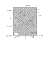
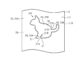
- the non-driving region 21 shown in FIG. 1 has a shape like an elongated line, and is bent at a plurality of points between one end 21A and the other end 21B.
- the non-driving area 21 defines the driving area 20 into a driving area 20B having a predetermined symbol shape and a driving area 20A located outside the driving area 20B. Further, the non-driving region 21 does not come into contact with or intersect between one end 21A and the other end 21B, and a distance of a predetermined distance or more is maintained. In FIG. 1, even in the region 101 in which the non-driving region 21 is close to each other, an interval is maintained between the non-driving regions 21.
- the drive regions 20A and 20B defined by the non-drive region 21 are electrically sandwiched between the grooves 120, that is, through a narrowed portion 30A located between the first portion and the second portion of the groove 120. Is conducted to.
- the drive electrode element 30 includes a conduction portion 26 sandwiched between the non-drive region 21 including the groove 120 and the floating electrode element 31.
- the width of the narrowed portion 30A is narrower than that of the drive regions 20A and 20B, and the drive regions 20A and 20B are connected.
- the non-driving region 21 and the narrowed portion 30A surround the driving region 20B.
- the drive region 20A corresponds to the outer region
- the drive region 20B corresponds to the inner region.
- connection area 24 is an area for applying a voltage signal to the drive area 20, and an external wiring 25 is connected to the connection area 24.
- the connection area 24 and the drive area 20 are adjacent to each other.
- the position where the connection area 24 is provided in the dimming sheet 10 is not particularly limited.
- the connection area 24 is located, for example, in a corner of the dimming sheet 10.
- the dimming sheet 10 shown in FIG. 1 displays one symbol by the non-driving region 21, a plurality of symbols may be displayed. That is, the dimming sheet 10 may have a plurality of independent non-driving regions 21 without being connected to each other.
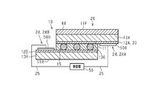
- FIG. 2 is a cross-sectional view taken along the line II-II in FIG. 1, showing a cross section of the dimming sheet 10 in the drive region 20 and the connection region 24.
- the thickness ratio of each layer in FIG. 2 is shown for convenience of explanation, and the thickness ratio of each layer is not limited to the thickness ratio shown in the figure.
- the light control sheet 10 has a light control layer 11, a first transparent electrode layer 12A, a second transparent electrode layer 12B, a first transparent support layer 13A, and a second transparent support layer 13B.
- the dimming layer 11 is sandwiched between the first transparent electrode layer 12A and the second transparent electrode layer 12B.
- the first transparent support layer 13A supports the surface of the first transparent electrode layer 12A opposite to the dimming layer 11 with the support surface 130 which is a single continuous surface, and the second transparent support layer 13B is the second.
- the surface of the transparent electrode layer 12B opposite to the dimming layer 11 is supported.
- the dimming layer 11 may have a single-layer structure or a multi-layer structure.
- the light control layer 11 having a multi-layer structure is a thin layer that enhances the adhesion between the functional layer having a light control function and the functional layer and the first transparent electrode layer 12A, and between the functional layer and the second transparent electrode layer 12B. May be provided.
- the dimming sheet 10 is provided with a protective layer 44.
- the protective layer 44 is located on the side opposite to the first transparent electrode layer 12A with respect to the first transparent support layer 13A.
- the protective layer 44 may be fixed to the first transparent support layer 13A via an adhesive layer (not shown).
- the first surface 11F of the dimming sheet 10 is the surface of the protective layer 44 opposite to the surface facing the first transparent support layer 13A.
- the second surface 11R of the dimming sheet 10 is a surface of the second transparent support layer 13B opposite to the surface facing the second transparent electrode layer 12B.
- the second surface 11R is attached to a transparent plate made of glass, resin, or the like via an adhesive layer (not shown).
- the transparent plate is, for example, a window glass provided in various buildings such as houses, stores, stations, and airports, a partition installed in an office, a show window installed in a store, or a window glass provided in a moving body such as a vehicle or an aircraft. And windshield.
- Each surface of the transparent plate may be a flat surface or a curved surface.
- the connection region 24 includes a first connection region 24A to which an external wiring 25 for applying a voltage signal to the first transparent electrode layer 12A is connected, and an external wiring 25 for applying a voltage signal to the second transparent electrode layer 12B. Includes a second connection area 24B to which is connected.
- the first connection region 24A is a region where the dimming layer 11, the second transparent electrode layer 12B, and the second transparent support layer 13B are absent, and the first transparent electrode layer 12A is exposed.
- the first terminal portion 50A is connected to the first transparent electrode layer 12A exposed in the first connection region 24A. That is, the drive electrode element 30 extends from the drive region 20 to the first connection region 24A, and in the first connection region 24A, the first terminal portion 50A is connected to the drive electrode element 30.
- the second connection region 24B is a region where the dimming layer 11, the first transparent electrode layer 12A, the first transparent support layer 13A, and the protective layer 44 are absent, and the second transparent electrode layer 12B is exposed.
- the second terminal portion 50B is connected to the second transparent electrode layer 12B exposed in the second connection region 24B.
- External wiring 25 extends from each of the first terminal portion 50A and the second terminal portion 50B, and these external wiring 25 are connected to the control unit 50.
- the control unit 50 applies a voltage signal to the drive electrode element 30 of the first transparent electrode layer 12A through the first terminal unit 50A, and applies a voltage signal to the second transparent electrode layer 12B through the second terminal unit 50B.
- the control unit 50 controls the potential difference between the first transparent electrode layer 12A and the second transparent electrode layer 12B in the drive region 20.
- the second transparent electrode layer 12B is controlled to, for example, a ground potential.
- a dimming device is configured from the dimming sheet 10 and the control unit 50.
- the dimming layer 11 includes a transparent polymer layer and a liquid crystal composition.
- the transparent polymer layer has voids in which the liquid crystal composition is filled.
- the liquid crystal composition is filled in the voids of the transparent polymer layer.
- the liquid crystal composition contains liquid crystal molecules.
- As the material of the liquid crystal composition a known material can be used.
- An example of a liquid crystal molecule is composed of a Schiff base type, an azo type, an azoxy type, a biphenyl type, a terphenyl type, a benzoic acid ester type, a trans type, a pyrimidine type, a cyclohexanecarboxylic acid ester type, a phenylcyclohexane type, and a dioxane type. It is one of the groups to be selected.
- the light control layer 11 has a single layer structure, the light control layer 11 is composed of only a functional layer including a transparent polymer layer and a liquid crystal composition.
- the holding type of the liquid crystal composition is one of a polymer network type, a polymer dispersed type, and a capsule type.
- the polymer network type includes a transparent polymer network having a three-dimensional network. The voids in the mesh are in communication with each other, and the liquid crystal composition is held in the voids in the mesh.
- the polymer network is an example of a transparent polymer layer.
- the polymer-dispersed type has a large number of isolated voids in the transparent polymer layer, and holds the liquid crystal composition in the voids dispersed in the polymer layer.
- the capsule type holds the liquid crystal composition having a capsule shape in the transparent polymer layer.
- the liquid crystal composition may contain a monomer for forming a transparent polymer layer, a dichroic dye, and the like.
- the light control layer 11 may include a spacer 15 for keeping the thickness of the light control layer 11 within a certain range.
- Each of the first transparent electrode layer 12A and the second transparent electrode layer 12B has conductivity and is transparent to light in the visible region.
- Known materials can be used for the first transparent electrode layer 12A and the second transparent electrode layer 12B.
- Materials for forming the first transparent electrode layer 12A and the second transparent electrode layer 12B include, for example, indium tin oxide, fluorine-doped tin oxide, tin oxide, zinc oxide, carbon nanotubes, and poly (3,4-ethylenedioxy). Thiofen) etc.
- Each of the first transparent support layer 13A and the second transparent support layer 13B is a base material that is transparent to light in the visible region.
- Known materials can be used for the first transparent support layer 13A and the second transparent support layer 13B.
- An example of the material for forming the first transparent support layer 13A and the second transparent support layer 13B may be a synthetic resin or an inorganic compound.
- the synthetic resin is, for example, polyester, polyacrylate, polycarbonate, polyolefin or the like.
- the polyester is, for example, polyethylene terephthalate, polyethylene naphthalate or the like.
- the polyacrylate is, for example, polymethylmethacrylate and the like.
- the inorganic compound is, for example, silicon dioxide, silicon oxynitride, silicon nitride and the like.
- Each of the first terminal portion 50A and the second terminal portion 50B includes, for example, a conductive adhesive layer and a wiring board.
- the conductive adhesive layer is, for example, an anisotropic conductive film (ACF: Anisotropic Conductive Film), an anisotropic conductive paste (ACP: Anisotropic Conductive Paste), an isotropic conductive film (ICF: Isotropic Conductive Film), or isotropic. It is formed from a conductive paste (ICP: Anisotropic Conductive Paste) or the like.
- the wiring board is, for example, a flexible printed circuit board (FPC).
- each of the first terminal portion 50A and the second terminal portion 50B may have a structure in which a conductive material such as a conductive tape and the external wiring 25 are joined by soldering or the like.
- the orientation of the liquid crystal molecules changes in response to the change in voltage generated between the first transparent electrode layer 12A and the second transparent electrode layer 12B.
- the change in the orientation of the liquid crystal molecules changes the degree of scattering, the degree of absorption, and the degree of transmission of visible light entering the dimming layer 11.
- the orientation of the liquid crystal molecules in the long axis direction is irregular.
- the degree of scattering of the light incident on the dimming layer 11 becomes large, and the drive region 20 looks muddy. That is, the drive region 20 is opaque when no voltage signal is applied to the dimming layer 11.
- the liquid crystal molecule when a voltage signal is applied to the first transparent electrode layer 12A and the second transparent electrode layer 12B and a potential difference of a predetermined value or more is generated between the first transparent electrode layer 12A and the second transparent electrode layer 12B, the liquid crystal molecule. Is oriented, and the long axis direction of the liquid crystal molecule is the direction along the electric field direction between the first transparent electrode layer 12A and the second transparent electrode layer 12B. As a result, light easily passes through the dimming layer 11, and the drive region 20 becomes transparent.
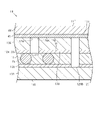
- FIG. 3 is a cross-sectional view taken along the line III-III in FIG. 1, including the non-driving region 21.
- the drive electrode element 30 is located in the drive region 20.
- the non-driving region 21 includes a floating region 22 in which the floating electrode element 31 is located and a boundary region 23 in which the groove 120 is located.
- the boundary region 23 does not include the electrode element. That is, the floating region 22 is defined by the boundary region 23 composed of the grooves 120.
- the driving electrode element 30 and the floating electrode element 31 are separate layered bodies arranged along the support surface 130 of the first transparent support layer 13A.
- the drive electrode element 30 and the floating electrode element 31 are separated by a groove 120.
- the groove 120 has an opening 122 on the dimming layer 11 side of the first transparent electrode layer 12A, penetrates the first transparent electrode layer 12A, and is in the thickness direction of the first transparent support layer 13A. It extends halfway.
- the drive electrode element 30 and the floating electrode element 31 are isolated from each other by being separated by the groove 120.
- the width L2 of the groove 120 may be smaller than the diameter of the spacer 15. As a result, the spacer 15 is prevented from entering the groove 120. Further, the groove 120 is filled with a liquid crystal composition.
- the liquid crystal composition may be filled in a part of the volume of the groove 120, and may not be filled in the entire volume. By filling the groove 120 with the liquid crystal composition, the groove 120 is inconspicuous when the dimming sheet 10 is visually recognized from the first surface 11F side or the second surface 11R side.
- FIG. 4 is an enlarged view of the region 101 in FIG.
- the drive regions 20A and 20B are connected by a narrowed portion 30A provided between the non-drive regions 21.
- the narrowed portion 30A may be positioned so as to connect the first portion and the second portion of the non-driving region 21 as shown in FIG.
- the narrowed portion 30A may be provided between the end portion 21A and the end portion 21B.
- the width L1 of the narrowed portion 30A is 1 mm or more in order to ensure the continuity between the drive region 20A outside the non-drive region 21 and the drive region 20B inside the non-drive region 21.
- the relative distance between different portions between one end 21A and the other end 21B of the non-driving region 21 including one groove 120 and the floating electrode element 31 which is the second electrode element is 1 mm or more. Is.
- the width L1 of the narrowed portion 30A is less than 1 mm, the resistance value of the narrowed portion 30A increases, the light transmittances of the drive regions 20A and 20B are not equal, and the drive region 20B is opaque even when a drive voltage is applied. There is a possibility that it will not change from a clear state to a transparent state.
- the width L1 of the narrowed portion 30A may be 30 mm or less in order to enhance the design. If the width L1 of the narrowed portion 30A exceeds 30 mm, the desired shape may not be obtained.
- the non-driving region 21 has a bent portion 102 that is curved or bent according to the design. As shown in FIG. 4, when the bent portion 102 of the non-driving region 21 is curved, the minimum value of the angle ⁇ 1 formed by the tangents 105 and 106 in contact with the different positions of the bent portion 102 is 10 degrees or more.
- the minimum value of the angle ⁇ 2 formed by the non-driving regions 21 is 10 degrees or more. .. If the angles ⁇ 1 and ⁇ 2 are less than 10 degrees, the first transparent support layer 13A and the first transparent electrode layer 12A may be peeled off after the step of forming or forming the groove 120. By setting the angles ⁇ 1 and ⁇ 2 to 10 degrees or more, peeling of the first transparent support layer 13A and the first transparent electrode layer 12A can be suppressed, and the pattern drawn by the non-driving region 21 can be clarified.
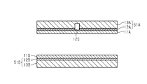
- a film 51A having a first transparent electrode layer 12A and a first transparent support layer 13A and a film 51B having a second transparent electrode layer 12B and a second transparent support layer 13B are prepared.
- a groove 120 is formed from the first transparent electrode layer 12A side on the film 51A provided with the first transparent electrode layer 12A and the first transparent support layer 13A by using a cutting plotter.
- the control device connected to the cutting plotter operates the cutting plotter according to a pre-input pattern to form the groove 120.
- the groove 120 may be formed by using a device other than the cutting plotter.
- the groove 120 may be formed in a blade other than the cutting plotter, a laser cutting device, or the first transparent electrode layer 12A.
- a laser cutting device for example, a laser equipped with a CO 2 laser can be used. When a laser cutting device is used, the portion irradiated with the laser beam can be directly destroyed to form the groove 120.
- a liquid material containing a spacer 15 containing divinylbenzene or the like as a main material and a dispersion medium for dispersing the spacer 15 is placed on the first transparent electrode layer 12A side and the second transparent film 51A and 51B of the films 51A and 51B. It is applied to the surface on the electrode layer 12B side. Further, the film on which the spacer 15 is sprayed is heated to remove the dispersion medium. At this time, the spacer 15 may be sprayed only on one of the films.
- the light control sheet 10 is a roll-to-roll method in which various steps are performed on the film conveyed from the upstream roll and wound on the downstream roll, and various steps are performed on the film cut to a predetermined size. It may be any of the single-wafer manufacturing processes. In either case, in the step of forming the groove 120, the film composed of the first transparent electrode layer 12A and the first transparent support layer 13A and the film composed of the second transparent electrode layer 12B and the second transparent support layer 13B are dimmed. This is done before pasting through the layer 11.
- a notch is made in the corner of the second surface 11R of the light control sheet 10 having a predetermined size, and the second transparent support layer 13B and the second transparent electrode layer 12B are peeled off. Further, the dimming layer 11 is removed and the first transparent electrode layer 12A is exposed to form the connection region 24. Similarly, the connection region 24 is also formed at the corner of the first surface 11F. Then, the first terminal portion 50A and the second terminal portion 50B are formed, and the external wiring 25 is connected to the connection region 24. Further, the connection region 24 is sealed with an epoxy resin or the like. Further, the step of attaching the protective layer 44 to the first transparent support layer 13A may be performed after attaching a pair of films.
- the grooves 120 By forming the grooves 120 by making cuts in the first transparent electrode layer 12A and the first transparent support layer 13A in this way, for example, forming a resist mask required for patterning, exposure, development, etching, removal of the resist mask, and The groove 120 can be easily formed as compared with a manufacturing method including steps such as cleaning.
- FIG. 7 schematically shows the degree of transparency of the dimming sheet 10 when the dimming sheet 10 is not driven, that is, when no voltage signal is applied to the first transparent electrode layer 12A and the second transparent electrode layer 12B. ..
- both the drive region 20 and the non-drive region 21 are opaque. Therefore, the entire surface of the dimming sheet 10 looks whitish and muddy, for example, and images such as characters and patterns formed by the non-driving region 21 are not visible.
- the groove 120 has a depth that penetrates the first transparent electrode layer 12A and does not penetrate the first transparent support layer 13A, the groove 120 can be seen from either the first surface 11F or the second surface 11R of the dimming sheet 10. 120 is inconspicuous. In addition, by filling the groove 120 with the dimming material, the groove 120 can be made less visible. As a result, the aesthetic appearance of the dimming sheet 10 when displaying the design is enhanced.
- the drive region 20 becomes transparent, while the non-drive region 21 is opaque. Therefore, only the non-driving region 21 looks whitish and muddy, for example, and an image of a pattern such as a character or a pattern composed of the non-driving region 21 can be visually recognized.
- a voltage signal is applied to the drive region 20B surrounded by the non-drive region 21 and the drive region 20A outside the drive region 20B to become transparent.
- the light control sheet 10 of the present embodiment regions having different light transmittances are formed in the plane of the light control sheet 10, and the difference in light transmittance between these regions is adjusted. Appears only when the optical sheet 10 is driven. Therefore, when the dimming sheet 10 is driven, the space in which the dimming sheet 10 is arranged can be decorated by visually recognizing images such as characters and patterns formed by the non-driving region 21. By switching between driving and non-driving of the dimming sheet 10, the presence or absence of the appearance of the image can be switched, so that the decorative state of the space can be dynamically changed. Therefore, it is possible to improve the design of the dimming sheet 10.
- the dimming sheet 10 is obtained by applying a voltage signal to only one of the drive electrode element 30 and the floating electrode element 31, or by applying different voltage signals to the drive electrode element 30 and the floating electrode element 31.
- the light transmission rate between the drive region 20 where the drive electrode element 30 is located and the non-drive region 21 where the floating electrode element 31 is located can be changed. Therefore, by changing the application state of the voltage signal to those regions, it is possible to make the design appear on the dimming sheet 10, so that the design of the dimming sheet 10 is improved.
- the width of the narrowed portion 30A provided in the drive electrode element 30 is 1 mm or more, the first transparent electrode layer 12A or the first transparent support layer 13A is peeled off after the groove 120 forming step or the groove 120 forming. Etc. are unlikely to occur. Further, since the relative distance of the grooves 120 is always maintained at 1 mm or more, even if different portions of the same groove 120 or different grooves 120 are close to each other, conduction in the same electrode element is performed in the close portion. Sex can be ensured. Therefore, it is possible to suppress the conduction failure caused by the increase in resistance in the close portion and appropriately control the light transmittance of the drive electrode element 30 and the floating electrode element 31. Therefore, since the design can be clearly displayed on the dimming sheet 10, the design of the dimming sheet 10 can be enhanced.
- the angle of the bent portion 102 of the non-driving region 21 or the angle formed by the tangents 105 and 106 of the bent portion 102 is 10 degrees or more, the first transparent electrode layer 12A or the first transparent electrode layer 12A or the first in the groove 120 forming step.
- the transparent support layer 13A is less likely to be peeled off, and the drive electrode element 30 and the floating electrode element 31 can be easily formed into a desired shape. Therefore, the design can be clearly displayed on the dimming sheet 10.
- the groove 120 that divides the drive region 20 and the non-drive region 21 has a depth that penetrates the first transparent electrode layer 12A and does not penetrate the first transparent electrode layer 12A, it is inside the first transparent support layer 13A. On the surface opposite to the support surface, light scattering by the groove 120 is suppressed. As a result, the groove 120 can be made inconspicuous when the dimming sheet 10 is viewed from the first transparent electrode layer 12A side from at least a position facing the opposite surface. Therefore, the aesthetic appearance of the dimming sheet 10 can be improved.
- FIG. 8 shows a cross section of the dimming sheet 10.
- the drive electrode element 30 and the floating electrode element 31 are separated by a groove 120.
- the groove 120 extends in the thickness direction of the first transparent electrode layer 12A.
- the groove 120 extends in the thickness direction of the first transparent electrode layer 12A and the first transparent support layer 13A, and penetrates the first transparent electrode layer 12A and the first transparent support layer 13A.
- the groove 120 has an opening 122 located on the dimming layer 11 side of the first transparent electrode layer 12A and an opening 124 located on the opposite side of the first transparent electrode layer 12A of the first transparent support layer 13A. is doing.
- the drive electrode element 30 and the floating electrode element 31 are isolated from each other by being separated by the groove 120.
- the opening 124 of the groove 120 is sealed by the protective layer 44 via the adhesive layer 45.
- the adhesive layer 45 may be any material that can join the protective layer 44 and the first transparent support layer 13A and has translucency.
- the adhesive layer 45 is a transparent adhesive film (Optical Clear Adhesive Film), and joins the first transparent support layer 13A and the protective layer 44.
- a film 51A provided with the first transparent electrode layer 12A and the first transparent support layer 13A and a film 51B provided with the second transparent electrode layer 12B and the second transparent support layer 13B are prepared. .. Further, the spacer 15 is sprayed on the films 51A and 51B, and a dimming material containing a transparent polymer material and a liquid crystal composition is applied. The dimming layers 11A and 11B are formed, and a pair of films 51A and 51B are laminated and bonded while applying a pressure of a predetermined magnitude.
- a groove 120 is formed by making a notch from the surface 131 on the side opposite to the support surface 130 of the first transparent support layer 13A until it reaches the dimming layer 11.
- the method of forming the groove 120 is the same as that of the first embodiment.
- the adhesive layer 45 and the protective layer 44 are laminated on the surface 131 of the first transparent support layer 13A.
- the groove 120 does not have to be formed after forming the laminated body in which the dimming layer 11 is sandwiched between the films 51A and 51B.
- the groove 120 has a step of forming a dimming layer 11A and a step of laminating the films 51A and 51B between the step of spraying the spacer 15 and the step of applying the dimming material before the step of spraying the spacer 15 on the film 51A. It may be formed in any step before forming the laminate, such as between steps.
- the groove 120 has a depth that penetrates the first transparent support layer 13A and the second transparent support layer, the first transparent support layer 13A, the first transparent electrode layer 12A, and the like. It is also possible to form the groove 120 after laminating the dimming layer, the second transparent electrode layer and the second transparent support layer, and it is also possible to form the groove 120 in the process of laminating them. Therefore, the degree of freedom in the manufacturing process can be increased.
- FIG. 9 shows a dimming sheet 10 provided with a plurality of non-driving regions 21.
- the non-driving region 21 includes a floating region 22 and a boundary region 23.
- the boundary region 23 has a frame-like shape.
- the boundary region 23 defines a floating region 22 which is a closed region.
- the boundary region 23 provided on the dimming sheet 10 shown in the example of FIG. 9 surrounds the star-shaped floating region 22.
- the dimming sheet 10 is provided with different non-driving regions 21 that are independent of each other. Between each of the non-driving regions 21, a narrowed portion 30A sandwiched between different grooves 120 is provided.
- the narrowed portion 30A is a portion whose width is narrowed due to the proximity of different non-driving regions 21 to each other, and is a conductive portion 27 that conducts the driving region 20 around the narrowed portion 30A.
- the width L3 of the narrowed portion 30A is 1 mm or more. That is, the relative distance between the different non-driving regions 21 is 1 mm or more. If the width L3 of the narrowed portion 30A is less than 1 mm, the conductivity of the narrowed portion 30A may decrease, and the light transmittances of the drive regions 20 connected via the narrowed portion 30A may not be equal.
- the dimming sheet 10 shown in FIG. 9 has two non-driving regions 21, it may have three or more non-driving regions 21.
- the groove 120 has a closed frame-like shape surrounding the floating electrode element 31.
- the groove 120 may not have a closed frame shape surrounding the floating electrode element 31 as long as it extends along the support surface 130 of the first transparent support layer 13A.
- the groove 120 extends from a start point located at the first end on one of the four sides of the rectangular dimming sheet 10 to an end point located at the second end through the outer circumference of the floating region 22. May be.
- the second end may be located on the same side as the first end of the four sides of the dimming sheet 10, or may be located on a different side.
- the start point and the end point of the groove 120 may be located at the end of the dimming sheet 10.
- the dimming sheet 10 is a normal type, but when a voltage signal is not applied, the incident light is transmitted to increase the translucency, and when the voltage signal is applied, the incident light is transmitted. It may be a reverse type (reverse type) that scatters and reduces the translucency.
- FIG. 10 shows an example of a reverse type dimming sheet 10.
- the reverse type dimming sheet 10 includes a functional layer 111 including a transparent polymer layer and a liquid crystal composition, a first alignment layer 112, and a second alignment layer 113.
- the first alignment layer 112 and the second alignment layer 113 constitute the dimming layer 11.
- the first alignment layer 112 is located between the dimming layer 11 and the first transparent electrode layer 12A, and is in contact with these layers.
- the second alignment layer 113 is located between the dimming layer 11 and the second transparent electrode layer 12B, and is in contact with these layers.
- Each of the first alignment layer 112 and the second alignment layer 113 is, for example, a vertical alignment film or a horizontal alignment film.
- the vertically oriented film orients the long axis direction of the liquid crystal molecules along the thickness direction of the dimming layer 11.
- the horizontally aligned film orients the long axis direction of the liquid crystal molecules along a direction substantially orthogonal to the thickness direction of the dimming layer 11. In this way, the first alignment layer 112 and the second alignment layer 113 regulate the orientation of the plurality of liquid crystal molecules included in the dimming layer 11.
- the material for forming each of the first alignment layer 112 and the second alignment layer 113 is an organic compound, an inorganic compound, and a mixture thereof.
- the organic compound are polyimide, polyamide, polyvinyl alcohol, cyanide compound and the like.
- the inorganic compound is, for example, silicon oxide, zirconium oxide, or the like.
- the material for forming the first alignment layer 112 and the second alignment layer 113 may be silicone. Silicone is a compound having an inorganic part and an organic part.
- the groove 120 has an opening 122 on the dimming layer 11 side of the first alignment layer 112, penetrates the first alignment layer 112 and the first transparent electrode layer 12A, and does not penetrate the first transparent electrode layer 12A. That is, the depth of the groove 120 is smaller than the sum of the thickness of the first alignment layer 112, the thickness of the first transparent electrode layer 12A, and the thickness of the first transparent support layer 13A.
- the groove 120 is partially filled with the dimming layer 11. Further, the groove 120 may penetrate the first transparent support layer 13A as in the second embodiment.
- the light control sheet 10 includes the first alignment layer 112 and the second alignment layer 113
- the liquid crystal molecule when no voltage signal is applied to the first transparent electrode layer 12A and the second transparent electrode layer 12B in the drive region 20, the liquid crystal molecule.
- the orientation in the long axis direction is along the thickness direction of the dimming layer 11. Therefore, the drive region 20 is transparent.
- the drive region 20 when a voltage signal is applied to the first transparent electrode layer 12A and the second transparent electrode layer 12B, the orientation of the liquid crystal molecules in the major axis direction intersects with the thickness direction of the dimming layer 11. It will be oriented. Therefore, the drive region 20 looks muddy and becomes opaque.
- the dimming sheet 10 includes the first alignment layer 112 and the second alignment layer 113, in the floating region 22 and the boundary region 23, the orientation of the liquid crystal molecules in the major axis direction is always along the thickness direction of the dimming layer 11.
- the non-driving region 21 is always transparent because it is oriented.
- the drive area 20 is transparent, and images such as characters and patterns formed by the non-drive area 21 are not visible.
- the drive region 20 becomes opaque, while the non-drive region 21 is transparent, so that images such as characters and patterns formed by the non-drive region 21 can be visually recognized.
- the light control sheet 10 includes the first alignment layer 112 and the second alignment layer 113, regions having different light transmittances are formed in the plane of the light control sheet 10 and the light transmittance is different from each other. The difference in light transmittance in these regions appears only when the dimming sheet 10 is driven. Therefore, it is possible to improve the design of the dimming sheet 10.
- the groove 120 penetrates the first alignment layer 112, but after forming the groove 120 in the laminate composed of the first transparent electrode layer 12A and the first transparent support layer 13A, the first alignment layer 112 May be formed.
- the first alignment layer 112 is formed along the bottom surface and the side surface of the groove 120. Even in this way, the groove 120 can be made inconspicuous when viewed from the outside.
- the grooves 120 are located at the same depth in the stacking direction (thickness direction) of the layers constituting the dimming sheet 10.
- each of the plurality of grooves 120 may be located at different depths in the stacking direction. Examples thereof are listed in FIGS. 11 to 13, and in each of those examples, the method of each of the above-described embodiments can be used as the method for forming the groove 120.
- the dimming sheet 10 is described as a normal type, it may be applied to a reverse type.
- FIGS. 11 to 13 show a state in which the groove 120 is not filled with the dimming material, at least a part of the groove 120 may be filled with the dimming material.
- One of the grooves 120A shown in FIG. 11 penetrates the first transparent support layer 13A and the first transparent electrode layer 12A.
- the other groove 120B penetrates only the second transparent electrode layer 12B.
- the groove 120B may be formed from the second transparent support layer 13B side by a laser cutting device or the like.
- FIG. 12 shows another example in which each of the plurality of grooves 120 is formed at different positions in the stacking direction.
- a plurality of grooves 120 are formed by making a notch from the first transparent support layer 13A side.
- One groove 120A penetrates the first transparent support layer 13A and the first transparent electrode layer 12A.
- the other groove 120B penetrates the dimming layer 11 and the second transparent electrode layer 12B in addition to the first transparent support layer 13A and the first transparent electrode layer 12A.
- the groove 120 may be filled with a light control material.
- FIG. 13 shows another example in which each of the plurality of grooves 120 is formed at different positions in the stacking direction.
- One groove 120A penetrates the first transparent support layer 13A and the first transparent electrode layer 12A.
- the other groove 120B penetrates the second transparent support layer 13B and the second transparent electrode layer 12B.
- the grooves 120A and 120B are arranged so as not to overlap each other. May be good.
- the region where the grooves 120A and 120B are formed becomes the boundary region 23.
- the strength of the region sandwiched between the grooves 120A and 120B and the vicinity thereof tends to decrease, but as in the above example, each of the plurality of grooves 120 tends to decrease.
- a voltage signal is applied to the drive electrode element 30 which is the first electrode element, and no voltage signal is applied to the floating electrode element 31 which is the second electrode element.
- voltage signals may be applied separately to the first electrode element and the second electrode element.
- a wiring for applying a voltage signal to the second electrode element is connected to the end of the second electrode element.
- the terminal portion connected to the first electrode element and the terminal portion connected to the second electrode element are separate terminal portions for each voltage signal.
- the first region where the first electrode element is located is switched between transparent and opaque by switching the application state of the voltage signal to the first electrode element.
- the second region where the second electrode element is located is switched between transparent and opaque independently of the first region by switching the application state of the voltage signal to the second electrode element.
- both the first region and the second region are opaque, the first region is opaque and the second region is transparent, the first region is transparent and the second region is opaque, and the first region is opaque. It is possible to switch between four states, one in which the region and the second region are both opaque. Therefore, since the decorative state of the space by the dimming sheet 10 can be changed more variously, the design of the dimming sheet 10 can be further improved.
- the light transmittance of at least one of the first region and the second region may be controlled to the light transmittance corresponding to the transparency and the opacity.
- the potential difference between the first transparent electrode layer 12A and the second transparent electrode layer 12B is within a predetermined range, the potential difference is changed.
- the light transmittance of the light control sheet 10 gradually changes. Therefore, in the first region or the second region, the potential difference between the first transparent electrode layer 12A and the second transparent electrode layer 12B is set to a value between the potential difference at which the region becomes transparent and the potential difference at which the region becomes opaque.
- the region can be controlled to be translucent with a light transmittance between transparent and opaque.
- the first region is switched between transparent and opaque by switching the application state of the voltage signal to the first electrode element
- the second region is the application of the voltage signal to the second electrode element.
- the state By switching the state, it can be switched between translucent and opaque.
- the first region is transparent, the second region is controlled to be translucent. According to such a configuration, it is possible to switch between a state in which both the first region and the second region are opaque and a state in which the first region is opaque and the second region is translucent. This also makes it possible to improve the design of the dimming sheet 10.
- the drive regions 20A and 20B defined by the non-drive region 21 are electrically conductive with each other via one narrowed portion 30A.
- the drive regions 20A and 20B defined by the non-drive region 21 may be electrically conductive with each other via the plurality of narrowed portions 30A.
- the drive electrode element 30 includes a plurality of conductive portions 26 sandwiched between the non-drive regions 21.
- the narrowed portion 30A has the same configuration as that of the first embodiment.
- the drive regions 20A and 20B may be electrically conductive with each other via the two narrowed portions 30A.
- the width of the narrowed portion 30A is 1 mm or more.
- the dimming sheet 10 may include a first electrode element and a wide groove 120C.
- the dimming sheet 10 includes a first electrode element that changes the light transmittance according to an application state of a voltage signal and a wide groove 120C, and does not include a second electrode element.
- the wide groove 120C can be rephrased as a recess.
- the entire character "C" is composed of the groove 120C.
- the region where the groove 120C is formed does not include the electrode element.
- the groove 120C is filled with at least one of the liquid crystal composition, the transparent polymer layer and the liquid crystal composition.
- the groove 120C may be filled with a substance other than the transparent polymer layer and the liquid crystal composition, or may be a void not filled with the substance.
- the drive region 20 and the groove 120C in which the groove 120C is not formed are both opaque.
- the drive region 20 becomes transparent, while the groove 120C is opaque. Therefore, only the groove 120C looks whitish and muddy, for example, and an image of a pattern such as a character or a pattern composed of the groove 120C can be visually recognized. In the example of FIG. 15, the letter "C" becomes visible.
- the width L30 of the narrowed portion 30A defined by the plurality of grooves 120C is 1 mm or more. Further, the width L10 of the narrowed portion 30A formed by one groove 120C is 1 mm or more.
- the definition of the narrowed portion 30A is the same as that of the above embodiment.
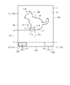
- the first connection region 24A which is an example of the non-drive region, includes the first terminal portion 50A and is bordered by a portion of the first transparent electrode layer 12A exposed from the dimming layer 11. ing.
- the second connection region 24B which is another example of the non-driving region, includes the second terminal portion 50B and is bordered by a portion of the second transparent electrode layer 12B exposed from the dimming layer 11.
- the first connection area 24A and the second connection area 24B are arranged in the first direction.
- the first direction is the direction in which the end side 10A of the dimming sheet 10 extends, and is the left-right direction in FIG.
- the shortest distance between the straight line passing through the groove 120 and extending in the first direction and the straight line passing through the first connection region 24A and extending in the first direction is the relative distance L6.
- the relative distance L6 is preferably 5 mm or more and 50 mm or less, and more preferably 5 mm or more and 20 mm or less. That is, the relative distance L6 is the distance between the first connection region 24A and the second connection region 24B and the groove 120 in the direction orthogonal to the end side 10A of the dimming sheet 10.
- the relative distance L6 is particularly preferably 5 mm or more and 50 mm or less.
- the unit area is an area adjacent to the first connection area 24A and an area adjacent to the second connection area 24B. The unit area passes through the first connection area 24A and is separated from the first connection area 24A by a straight line extending in the first direction.
- the length of the unit region in the first direction is 100 mm, and the length of the unit region in the second direction orthogonal to the first direction is 100 mm.
- the floating element ratio is the ratio of the area of the floating electrode element 31 to the sum of the areas of the driving electrode element 30 which is the first electrode and the floating electrode element 31 which is the second electrode element.
- the peel strength of the layer supporting the dimming layer 11 with respect to the dimming layer 11 is preferably 0.01 N or more.
- the peel strength at the portion including the narrowed portion 30A is measured by a method according to "6.99.3a) 180 degree peeling test" in JIS A 5759: 2016.
- the light control sheet 10 is a normal type, it is the peel strength of the first transparent electrode layer 12A with respect to the light control layer 11.
- the light control sheet 10 is a normal type, it is the peel strength of the first alignment layer 112 with respect to the light control layer 11. According to this aspect, peeling of the layer supporting the dimming layer 11 is suppressed in the narrowed portion 30A.
- the width of the narrowed portion 30A is 2 mm or more, and the peel strength per unit width (10 mm) of the narrowed portion 30A is 0.1 N or more. According to this aspect, peeling of the layer supporting the dimming layer 11 is further suppressed in the narrowed portion 30A.
- the film 51A before forming the narrowed portion 30A preferably has a peel strength of 0.4 N / 25 mm for the layer supporting the dimming layer 11 with respect to the dimming layer 11.
- a narrowed portion 30A having a width of 2 mm or more is formed on the film 51A.
- the peel strength is measured by a method according to "6.9.3a) 180 degree peeling test" in JIS A 5759: 2016. Thereby, even when the narrowed portion 30A having a width narrowed to about 2 mm is formed, it is possible to suppress the peeling in the narrowed portion 30A.
- Example 1 ⁇ Preparation of measurement sample 1> (Example 1) An embodiment, which is an example of each of the above embodiments, will be specifically described. It should be noted that these examples do not limit the present disclosure.
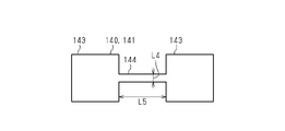
- a rectangular resistance value measurement region 143 was formed on a substrate having a transparent electrode layer 140 and a transparent support layer 141, and the resistance value measurement region 143 had a size of 50 mm ⁇ 25 mm. Further, two resistance value measurement regions 143 were connected via a narrowed portion 144 (conducting portion) having a width L4 of 50 mm and a length L5 of 100 mm to prepare a measurement sample. Further, a tester was connected to two resistance value measurement regions 143 to measure the resistance value.
- Example 2 A measurement sample was prepared in the same manner as in Example 1 except that the width L4 of the narrowed portion 144 was set to 30 mm.
- Example 3 A measurement sample was prepared in the same manner as in Example 1 except that the width L4 of the narrowed portion 144 was set to 10 mm.
- Example 4 A measurement sample was prepared in the same manner as in Example 1 except that the width L4 of the narrowed portion 144 was set to 5 mm.
- Example 5 A measurement sample was prepared in the same manner as in Example 1 except that the width L4 of the narrowed portion 144 was set to 2 mm.
- Example 6 A measurement sample was prepared in the same manner as in Example 1 except that the width L4 of the narrowed portion 144 was set to 1 mm.
- the resistance value was measured using a digital multimeter (manufactured by Yokogawa Test & Measurement Corporation, TY530).
- the resistance values ( ⁇ ) of Examples 1 to 6 are “494”, “719”, “1,225”, “2,259”, “5,220”, and “10,900”. , And increased as the width L4 of the narrowed portion 144 became smaller. In Comparative Example 1, the resistance value was "26,800", which was dramatically larger than that of Examples 1 to 5.
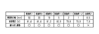
- Example 7 A dimming sheet having a laminated structure similar to that of the dimming sheet 10 shown in FIG. 2 was prepared. Further, rectangular characteristic measurement regions having a size of 50 mm ⁇ 25 mm were secured at two locations separated from each other, and these characteristic measurement regions were connected by a narrowed portion. The narrowed portion had a width of 50 mm and a length of 100 mm. Further, similarly to the dimming sheet 10 shown in FIG.
- a notch is made in the corner of one surface (second surface), the transparent support layer and the transparent electrode layer are peeled off, and the liquid crystal is removed to form a connection region. did. Similarly, a notch was made in the corner of one surface (first surface), the transparent support layer and the transparent electrode layer were peeled off, and the liquid crystal was removed to form a connection region. Then, external wiring was connected to these connection areas to enable control of the voltage applied to the characteristic measurement area.
- Example 8 A measurement sample was prepared in the same manner as in Example 7 except that the width of the narrowed portion was set to 30 mm.
- Example 9 A measurement sample was prepared in the same manner as in Example 7 except that the width of the narrowed portion was 10 mm.
- Example 10 A measurement sample was prepared in the same manner as in Example 7 except that the width of the narrowed portion was 5 mm.
- Example 11 A measurement sample was prepared in the same manner as in Example 7 except that the width of the narrowed portion was set to 2 mm.
- Example 12 A measurement sample was prepared in the same manner as in Example 7 except that the width of the narrowed portion was set to 1 mm.
- Comparative Example 2 A measurement sample was prepared in the same manner as in Example 7 except that the width of the narrowed portion was 0.5 mm.
Landscapes
- Physics & Mathematics (AREA)
- Nonlinear Science (AREA)
- Chemical & Material Sciences (AREA)
- Mathematical Physics (AREA)
- Crystallography & Structural Chemistry (AREA)
- General Physics & Mathematics (AREA)
- Optics & Photonics (AREA)
- Liquid Crystal (AREA)
- Geometry (AREA)
- Dispersion Chemistry (AREA)
Priority Applications (3)
| Application Number | Priority Date | Filing Date | Title |
|---|---|---|---|
| CN202180076080.7A CN116438485A (zh) | 2020-11-17 | 2021-11-17 | 调光片以及调光片的制造方法 |
| EP21894694.5A EP4249995A4 (en) | 2020-11-17 | 2021-11-17 | LIGHT CONTROL SHEET AND METHOD FOR PRODUCING LIGHT CONTROL SHEET |
| US18/318,175 US12044940B2 (en) | 2020-11-17 | 2023-05-16 | Light control sheet and method of producing light control sheet |
Applications Claiming Priority (2)
| Application Number | Priority Date | Filing Date | Title |
|---|---|---|---|
| JP2020191233A JP7067599B1 (ja) | 2020-11-17 | 2020-11-17 | 調光シート及び調光シートの製造方法 |
| JP2020-191233 | 2020-11-17 |
Related Child Applications (1)
| Application Number | Title | Priority Date | Filing Date |
|---|---|---|---|
| US18/318,175 Continuation US12044940B2 (en) | 2020-11-17 | 2023-05-16 | Light control sheet and method of producing light control sheet |
Publications (1)
| Publication Number | Publication Date |
|---|---|
| WO2022107821A1 true WO2022107821A1 (ja) | 2022-05-27 |
Family
ID=81606804
Family Applications (1)
| Application Number | Title | Priority Date | Filing Date |
|---|---|---|---|
| PCT/JP2021/042264 Ceased WO2022107821A1 (ja) | 2020-11-17 | 2021-11-17 | 調光シート及び調光シートの製造方法 |
Country Status (5)
| Country | Link |
|---|---|
| US (1) | US12044940B2 (https=) |
| EP (1) | EP4249995A4 (https=) |
| JP (2) | JP7067599B1 (https=) |
| CN (1) | CN116438485A (https=) |
| WO (1) | WO2022107821A1 (https=) |
Citations (3)
| Publication number | Priority date | Publication date | Assignee | Title |
|---|---|---|---|---|
| JPH09330609A (ja) * | 1995-12-05 | 1997-12-22 | Matsushita Electric Ind Co Ltd | バックライト装置及びカラー表示装置 |
| CN110554529A (zh) * | 2018-10-10 | 2019-12-10 | 邝永彪 | 调光层叠体及加工方法、双层蚀刻调光层叠体加工方法 |
| JP2020003644A (ja) * | 2018-06-28 | 2020-01-09 | 凸版印刷株式会社 | 調光シート、調光装置、および、調光シートの製造方法 |
Family Cites Families (17)
| Publication number | Priority date | Publication date | Assignee | Title |
|---|---|---|---|---|
| JPH06186525A (ja) * | 1992-12-18 | 1994-07-08 | Aronshiya:Kk | 装飾用板材 |
| US5629785A (en) * | 1995-05-04 | 1997-05-13 | Motorola, Inc. | Polymer dispersed liquid crystal display device with asymmetric optical diffuser |
| CN1162743C (zh) * | 1999-06-23 | 2004-08-18 | 时至准钟表股份有限公司 | 液晶显示装置 |
| CN100407428C (zh) * | 2002-02-12 | 2008-07-30 | 精工爱普生株式会社 | 薄膜半导体器件、电光装置及其制造方法 |
| JP2013105031A (ja) * | 2011-11-14 | 2013-05-30 | Hosiden Corp | 液晶表示装置 |
| US20170017100A1 (en) * | 2015-07-17 | 2017-01-19 | Iris Optronics Inc. | Smart curtain film |
| TWM517348U (zh) * | 2015-11-27 | 2016-02-11 | Nano Bit Tech Co Ltd | 多層顯示高分子分散液晶智慧窗 |
| JP2018045135A (ja) | 2016-09-15 | 2018-03-22 | 凸版印刷株式会社 | 調光フィルム、及びそれを用いた調光装置並びにスクリーン |
| JP2018185490A (ja) * | 2017-04-27 | 2018-11-22 | 大日本印刷株式会社 | 仕切り部材 |
| KR20190023522A (ko) * | 2017-08-29 | 2019-03-08 | 엘지이노텍 주식회사 | 전기변색소자 및 이를 포함하는 전기변색장치 |
| JP2019105680A (ja) * | 2017-12-11 | 2019-06-27 | 凸版印刷株式会社 | 調光装置 |
| EP4517417A3 (en) * | 2017-12-28 | 2025-05-28 | Toppan Printing Co., Ltd. | Light control sheet and light control window |
| JP7281254B2 (ja) * | 2018-07-24 | 2023-05-25 | スタンレー電気株式会社 | 車両用灯具 |
| CN210666261U (zh) * | 2019-07-23 | 2020-06-02 | 珠海兴业新材料科技有限公司 | 一种激光直接刻蚀制备的有图案和/或文字的液晶调光膜 |
| CN210401927U (zh) * | 2019-09-10 | 2020-04-24 | 珠海兴业新材料科技有限公司 | 一种含纳米银线透明导电膜的pdlc液晶调光膜 |
| JP7120291B2 (ja) * | 2020-11-17 | 2022-08-17 | 凸版印刷株式会社 | 調光シート及び調光シートの製造方法 |
| JP7001139B1 (ja) * | 2020-11-17 | 2022-01-19 | 凸版印刷株式会社 | 調光シート、および、調光シートの製造方法 |
-
2020
- 2020-11-17 JP JP2020191233A patent/JP7067599B1/ja active Active
-
2021
- 2021-11-17 WO PCT/JP2021/042264 patent/WO2022107821A1/ja not_active Ceased
- 2021-11-17 EP EP21894694.5A patent/EP4249995A4/en active Pending
- 2021-11-17 CN CN202180076080.7A patent/CN116438485A/zh active Pending
-
2022
- 2022-04-27 JP JP2022073169A patent/JP7494877B2/ja active Active
-
2023
- 2023-05-16 US US18/318,175 patent/US12044940B2/en active Active
Patent Citations (3)
| Publication number | Priority date | Publication date | Assignee | Title |
|---|---|---|---|---|
| JPH09330609A (ja) * | 1995-12-05 | 1997-12-22 | Matsushita Electric Ind Co Ltd | バックライト装置及びカラー表示装置 |
| JP2020003644A (ja) * | 2018-06-28 | 2020-01-09 | 凸版印刷株式会社 | 調光シート、調光装置、および、調光シートの製造方法 |
| CN110554529A (zh) * | 2018-10-10 | 2019-12-10 | 邝永彪 | 调光层叠体及加工方法、双层蚀刻调光层叠体加工方法 |
Non-Patent Citations (1)
| Title |
|---|
| See also references of EP4249995A4 * |
Also Published As
| Publication number | Publication date |
|---|---|
| US20230288761A1 (en) | 2023-09-14 |
| JP7494877B2 (ja) | 2024-06-04 |
| JP2022093468A (ja) | 2022-06-23 |
| JP7067599B1 (ja) | 2022-05-16 |
| EP4249995A4 (en) | 2024-05-29 |
| EP4249995A1 (en) | 2023-09-27 |
| JP2022080201A (ja) | 2022-05-27 |
| US12044940B2 (en) | 2024-07-23 |
| CN116438485A (zh) | 2023-07-14 |
Similar Documents
| Publication | Publication Date | Title |
|---|---|---|
| US11442320B2 (en) | Light control sheet and method of producing light control sheet | |
| JP7001139B1 (ja) | 調光シート、および、調光シートの製造方法 | |
| JP2004233999A (ja) | 光干渉型表示パネル及びその製造方法 | |
| JP7172181B2 (ja) | 調光シート、調光装置、および、調光シートの製造方法 | |
| JP2024149601A (ja) | 調光シート、および、調光装置 | |
| US12140840B2 (en) | Light control sheet and method of producing light control sheet | |
| JP7172262B2 (ja) | 調光フィルムおよびその製造方法 | |
| JP7067599B1 (ja) | 調光シート及び調光シートの製造方法 | |
| JP7753824B2 (ja) | 調光シート | |
| JP7753826B2 (ja) | 調光シート | |
| JP7753825B2 (ja) | 調光シート | |
| CN113641046A (zh) | 调光显示组件及装置、电子设备及调光显示组件的制作方法 | |
| JP7786212B2 (ja) | 調光シート | |
| US20260072317A1 (en) | Light control sheet and method of producing a light control sheet | |
| JP2023167679A (ja) | 調光シート、および調光シートの製造方法 |
Legal Events
| Date | Code | Title | Description |
|---|---|---|---|
| 121 | Ep: the epo has been informed by wipo that ep was designated in this application |
Ref document number: 21894694 Country of ref document: EP Kind code of ref document: A1 |
|
| NENP | Non-entry into the national phase |
Ref country code: DE |
|
| ENP | Entry into the national phase |
Ref document number: 2021894694 Country of ref document: EP Effective date: 20230619 |