WO2022107809A1 - 電力変換装置 - Google Patents
電力変換装置 Download PDFInfo
- Publication number
- WO2022107809A1 WO2022107809A1 PCT/JP2021/042240 JP2021042240W WO2022107809A1 WO 2022107809 A1 WO2022107809 A1 WO 2022107809A1 JP 2021042240 W JP2021042240 W JP 2021042240W WO 2022107809 A1 WO2022107809 A1 WO 2022107809A1
- Authority
- WO
- WIPO (PCT)
- Prior art keywords
- electrode side
- capacitance
- negative electrode
- positive electrode
- path
- Prior art date
- Legal status (The legal status is an assumption and is not a legal conclusion. Google has not performed a legal analysis and makes no representation as to the accuracy of the status listed.)
- Ceased
Links
Images


Classifications
-
- H—ELECTRICITY
- H02—GENERATION; CONVERSION OR DISTRIBUTION OF ELECTRIC POWER
- H02P—CONTROL OR REGULATION OF ELECTRIC MOTORS, ELECTRIC GENERATORS OR DYNAMO-ELECTRIC CONVERTERS; CONTROLLING TRANSFORMERS, REACTORS OR CHOKE COILS
- H02P23/00—Arrangements or methods for the control of AC motors characterised by a control method other than vector control
- H02P23/04—Arrangements or methods for the control of AC motors characterised by a control method other than vector control specially adapted for damping motor oscillations, e.g. for reducing hunting
-
- H—ELECTRICITY
- H02—GENERATION; CONVERSION OR DISTRIBUTION OF ELECTRIC POWER
- H02M—APPARATUS FOR CONVERSION BETWEEN AC AND AC, BETWEEN AC AND DC, OR BETWEEN DC AND DC, AND FOR USE WITH MAINS OR SIMILAR POWER SUPPLY SYSTEMS; CONVERSION OF DC OR AC INPUT POWER INTO SURGE OUTPUT POWER; CONTROL OR REGULATION THEREOF
- H02M1/00—Details of apparatus for conversion
- H02M1/44—Circuits or arrangements for compensating for electromagnetic interference in converters or inverters
-
- H—ELECTRICITY
- H02—GENERATION; CONVERSION OR DISTRIBUTION OF ELECTRIC POWER
- H02M—APPARATUS FOR CONVERSION BETWEEN AC AND AC, BETWEEN AC AND DC, OR BETWEEN DC AND DC, AND FOR USE WITH MAINS OR SIMILAR POWER SUPPLY SYSTEMS; CONVERSION OF DC OR AC INPUT POWER INTO SURGE OUTPUT POWER; CONTROL OR REGULATION THEREOF
- H02M1/00—Details of apparatus for conversion
- H02M1/12—Arrangements for reducing harmonics from AC input or output
- H02M1/123—Suppression of common mode voltage or current
-
- H—ELECTRICITY
- H02—GENERATION; CONVERSION OR DISTRIBUTION OF ELECTRIC POWER
- H02M—APPARATUS FOR CONVERSION BETWEEN AC AND AC, BETWEEN AC AND DC, OR BETWEEN DC AND DC, AND FOR USE WITH MAINS OR SIMILAR POWER SUPPLY SYSTEMS; CONVERSION OF DC OR AC INPUT POWER INTO SURGE OUTPUT POWER; CONTROL OR REGULATION THEREOF
- H02M1/00—Details of apparatus for conversion
- H02M1/12—Arrangements for reducing harmonics from AC input or output
- H02M1/126—Arrangements for reducing harmonics from AC input or output using passive filters
-
- H—ELECTRICITY
- H02—GENERATION; CONVERSION OR DISTRIBUTION OF ELECTRIC POWER
- H02M—APPARATUS FOR CONVERSION BETWEEN AC AND AC, BETWEEN AC AND DC, OR BETWEEN DC AND DC, AND FOR USE WITH MAINS OR SIMILAR POWER SUPPLY SYSTEMS; CONVERSION OF DC OR AC INPUT POWER INTO SURGE OUTPUT POWER; CONTROL OR REGULATION THEREOF
- H02M1/00—Details of apparatus for conversion
- H02M1/14—Arrangements for reducing ripples from DC input or output
-
- H—ELECTRICITY
- H02—GENERATION; CONVERSION OR DISTRIBUTION OF ELECTRIC POWER
- H02M—APPARATUS FOR CONVERSION BETWEEN AC AND AC, BETWEEN AC AND DC, OR BETWEEN DC AND DC, AND FOR USE WITH MAINS OR SIMILAR POWER SUPPLY SYSTEMS; CONVERSION OF DC OR AC INPUT POWER INTO SURGE OUTPUT POWER; CONTROL OR REGULATION THEREOF
- H02M7/00—Conversion of AC power input into DC power output; Conversion of DC power input into AC power output
- H02M7/42—Conversion of DC power input into AC power output without possibility of reversal
- H02M7/44—Conversion of DC power input into AC power output without possibility of reversal by static converters
- H02M7/48—Conversion of DC power input into AC power output without possibility of reversal by static converters using discharge tubes with control electrode or semiconductor devices with control electrode
- H02M7/53—Conversion of DC power input into AC power output without possibility of reversal by static converters using discharge tubes with control electrode or semiconductor devices with control electrode using devices of a triode or transistor type requiring continuous application of a control signal
- H02M7/537—Conversion of DC power input into AC power output without possibility of reversal by static converters using discharge tubes with control electrode or semiconductor devices with control electrode using devices of a triode or transistor type requiring continuous application of a control signal using semiconductor devices only, e.g. single switched pulse inverters
- H02M7/5387—Conversion of DC power input into AC power output without possibility of reversal by static converters using discharge tubes with control electrode or semiconductor devices with control electrode using devices of a triode or transistor type requiring continuous application of a control signal using semiconductor devices only, e.g. single switched pulse inverters in a bridge configuration
-
- H—ELECTRICITY
- H02—GENERATION; CONVERSION OR DISTRIBUTION OF ELECTRIC POWER
- H02M—APPARATUS FOR CONVERSION BETWEEN AC AND AC, BETWEEN AC AND DC, OR BETWEEN DC AND DC, AND FOR USE WITH MAINS OR SIMILAR POWER SUPPLY SYSTEMS; CONVERSION OF DC OR AC INPUT POWER INTO SURGE OUTPUT POWER; CONTROL OR REGULATION THEREOF
- H02M7/00—Conversion of AC power input into DC power output; Conversion of DC power input into AC power output
- H02M7/42—Conversion of DC power input into AC power output without possibility of reversal
- H02M7/44—Conversion of DC power input into AC power output without possibility of reversal by static converters
- H02M7/48—Conversion of DC power input into AC power output without possibility of reversal by static converters using discharge tubes with control electrode or semiconductor devices with control electrode
- H02M7/53—Conversion of DC power input into AC power output without possibility of reversal by static converters using discharge tubes with control electrode or semiconductor devices with control electrode using devices of a triode or transistor type requiring continuous application of a control signal
- H02M7/537—Conversion of DC power input into AC power output without possibility of reversal by static converters using discharge tubes with control electrode or semiconductor devices with control electrode using devices of a triode or transistor type requiring continuous application of a control signal using semiconductor devices only, e.g. single switched pulse inverters
- H02M7/539—Conversion of DC power input into AC power output without possibility of reversal by static converters using discharge tubes with control electrode or semiconductor devices with control electrode using devices of a triode or transistor type requiring continuous application of a control signal using semiconductor devices only, e.g. single switched pulse inverters with automatic control of output wave form or frequency
-
- H—ELECTRICITY
- H02—GENERATION; CONVERSION OR DISTRIBUTION OF ELECTRIC POWER
- H02P—CONTROL OR REGULATION OF ELECTRIC MOTORS, ELECTRIC GENERATORS OR DYNAMO-ELECTRIC CONVERTERS; CONTROLLING TRANSFORMERS, REACTORS OR CHOKE COILS
- H02P27/00—Arrangements or methods for the control of AC motors characterised by the kind of supply voltage
- H02P27/04—Arrangements or methods for the control of AC motors characterised by the kind of supply voltage using variable-frequency supply voltage, e.g. inverter or converter supply voltage
- H02P27/06—Arrangements or methods for the control of AC motors characterised by the kind of supply voltage using variable-frequency supply voltage, e.g. inverter or converter supply voltage using DC to AC converters or inverters
-
- H—ELECTRICITY
- H03—ELECTRONIC CIRCUITRY
- H03H—IMPEDANCE NETWORKS, e.g. RESONANT CIRCUITS; RESONATORS
- H03H7/00—Multiple-port networks comprising only passive electrical elements as network components
- H03H7/01—Frequency selective two-port networks
- H03H7/0115—Frequency selective two-port networks comprising only inductors and capacitors
Definitions
- the present invention relates to a power conversion device that applies a three-phase AC output to a motor.
- Patent Document 2 when the inductance or capacitance added for balancing is switched by the switch, new noise is generated due to the surge, and further, the control becomes complicated due to the switching. There is. Further, Patent Document 2 does not consider the parasitic capacitance between the winding of the motor and the housing, which is one of the noise outflow routes.
- Non-Patent Document 1 proposes an impedance balance method in a DC-DC converter.
- the parasitic capacitance between the midpoint of the arm of the switching element and the housing is small and the intermediate impedance is sufficiently large.
- Has a problem that it is difficult to balance and the effect is limited because the parasitic capacitance between the midpoint of the arm and the housing is large and the intermediate impedance is small.
- the present invention has been made to solve the above-mentioned conventional technical problems, and impedance balance can be relatively easily achieved even when a motor is driven by applying a three-phase AC output. It is an object of the present invention to provide a power conversion device capable of effectively suppressing noise due to a common mode current.
- the power conversion device of the present invention has an upper arm switching element and a lower arm switching element of each phase and applies a three-phase AC output to the motor, and the height of the positive side of the DC power supply and the upper arm switching element.
- the capacitance Zv on the positive electrode side path, the inductance Zg on the negative electrode side path, and the capacitance Zt between the parasitic capacitance generation point P on the positive electrode side and the reference potential conductor Based on the equilibrium condition of the bridge circuit composed of the parasitic capacity generation point N on the negative electrode side and the capacitance Zb between the reference potential conductors, the capacitance Zt between the parasitic capacitance generation point P on the positive electrode side and the reference potential conductor, and The feature is that the capacitance Zb between the parasitic capacitance generation point N on the negative electrode side and the reference potential conductor is set, and the intermediate additional impedance Zm1 is connected between the intermediate path and the motor.
- the power conversion device has a positive electrode side additional capacitance connected between the positive electrode side parasitic capacitance generation point P and the reference potential conductor, and a negative electrode side parasitic capacitance generation point N and a reference. It is characterized by having one or both of the negative electrode side additional capacitance connected to the potential conductor.
- the intermediate additional impedance Zm1 in each of the above inventions is any one of a normal mode coil, a three-phase common mode coil, and a ferrite core, or a combination of two of them, or , It is characterized by being composed of all of them.
- the power conversion device is provided for wiring between the control board that controls the switching of the upper and lower arm switching elements, the DC power supply, the control board, the upper and lower arm switching elements, and the motor in each of the above inventions. It is characterized in that the wiring member is provided and the intermediate additional impedance Zm1 is arranged on the wiring member.
- the power conversion device has the positive electrode side additional capacitance connected between the positive electrode side parasitic capacity generation point P and the reference potential conductor in the above invention, and the negative electrode side parasitic capacity generation point N and the reference potential. It is characterized in that one or both of the negative electrode side additional capacities connected to the conductor are provided, and the positive electrode side additional capacitance and / or the negative electrode side additional capacitance is arranged in the wiring member. do.
- the power conversion device according to claim 7 is characterized in that, in the invention of claim 5 or 6, the wiring member is a bus bar assembly formed by resin-molding a bus bar.
- the power conversion device of the invention of claim 8 includes an EMI filter connected between the DC power supply and the upper and lower arm switching elements in each of the above inventions, and the EMI filter is connected to both the positive electrode side path and the negative electrode side path, respectively. It is characterized by having a normal mode coil.
- the present invention is a power conversion device having an upper arm switching element and a lower arm switching element of each phase and applying a three-phase AC output to a motor, and is a positive potential side of a DC power supply and a high potential side of the upper arm switching element.
- the inductance of the positive path side path is Zv.
- the positive side It is composed of the path inductance Zv, the negative electrode side path inductance Zg, the positive capacitance side parasitic capacity generation point P and the capacitance Zt between the reference potential conductor, and the negative negative side parasitic capacitance generation point N and the capacitance Zb between the reference potential conductor.
- the additional capacitance on the positive electrode side is connected between the parasitic capacitance generation point P on the positive electrode side and the reference potential conductor, and / or the parasitic capacitance generation point N on the negative electrode side and the reference potential conductor. If the additional capacitance on the negative electrode side is connected between the two, it becomes easier to balance the impedance.
- the intermediate additional impedance Zm1 is composed of any one of a normal mode coil, a three-phase common mode coil, and a ferrite core, or a combination of two of them, or all of them. It is good to do.
- the common mode impedance can be increased and the outflow of the common mode current can be reduced.
- a normal mode coil as an intermediate additional impedance, it is possible to effectively suppress switching surges, and as a result, mode conversion between three-phase wires (normal mode to common mode) is suppressed. This makes it less susceptible to the parasitic capacitance between the motor and the reference potential conductor.
- the normal mode coil does not require the coupling of three-phase wires, so it can be arranged separately, there are few restrictions on the arrangement, and it is smaller than the common mode coil. easy. Further, since the noise reduction effect can be obtained even if it is not included in all three phases (for example, only two phases), there is an advantage that it is easy to use.
- a control board for controlling switching of the upper and lower arm switching elements, a DC power supply, a control board, an upper and lower arm switching element, and a wiring member provided for wiring between the motors are provided. If this is the case, the device can be downsized by arranging the intermediate additional impedance Zm1 on the wiring member.
- the device can be further miniaturized.
- the wiring member with a bus bar assembly made by molding a bus bar with a resin as in the invention of claim 7, it is possible to ensure seismic resistance while ensuring insulation.
- the EMI filter connected between the DC power supply and the upper and lower arm switching elements is provided with a normal mode coil connected to both the positive electrode side path and the negative electrode side path, respectively, to provide a normal mode. It is possible to suppress the inconvenience that the current flows out to the reference potential conductor as a common mode current.
- a normal mode coil to both the positive electrode side path and the negative electrode side path, the impedances on the positive electrode side and the negative electrode side can be made equal, and the degree of equilibrium can be maintained, maximizing the effect of impedance balance. It is possible to pull out to.
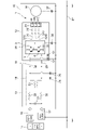
- FIG. 1 is an electric circuit diagram of a power conversion device 1 of an embodiment to which the present invention is applied
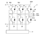
- FIG. 2 is an electric circuit diagram of an inverter circuit 2 and a control board 11.
- the power conversion device 1 of the embodiment is controlled by six switching elements 3 to 8 (FIG. 2) composed of IGBTs (may be MOSFETs) constituting the upper and lower arms of each phase of the three-phase inverter circuit 2 and printed wiring.
- a control board 11 (FIG. 2) on which a circuit is mounted, a battery 14, a control board 11, each switching element 3 to 8 described later, and a bus bar assembly 12 as a wiring member for wiring between the motors M.
- the filter substrate 13 is provided, and the DC power supplied from the battery 14 of the vehicle as a DC power source is converted into three-phase AC power and supplied to the stator coil (not shown) of the motor M.
- the motor M of the embodiment is composed of an IPMSM (Interior Permanent Magnet Synchronous Motor), and is housed in a metal (for example, aluminum) housing 15 of an electric compressor (for example, aluminum) of an electric compressor (for example, aluminum) mounted on a vehicle (not shown). It drives a compression mechanism, compresses the refrigerant, and discharges it into the refrigerant circuit of an air conditioner for vehicles (not shown). Then, it is assumed that the power conversion device 1 is integrally provided in the housing 15 of the electric compressor.
- IPMSM Interior Permanent Magnet Synchronous Motor
- Reference numeral 16 is a positive electrode side path connected to the positive electrode side (+) of the battery 14 via LISN (pseudo power supply network), and 17 is a negative electrode side path connected to the negative electrode side (-) of the battery 14 via LISN.
- An EMI filter 18 and a smoothing capacitor 19 are connected to the positive electrode side path 16 and the negative electrode side path 17.
- the EMI filter 18 and the smoothing capacitor 19 are connected between the battery 14 and the switching elements 3 to 8 of the inverter circuit 2.
- the EMI filter 18 has a normal mode connected to both the X capacitor 21 connected between the positive electrode side path 16 and the negative electrode side path 17 and both the positive electrode side path 16 and the negative electrode side path 17 in the subsequent stage of the X capacitor 21.
- the common mode coil 23 connected to the rear stages of the normal mode coils 22 and 35, and the rear stage of the common mode coil 23, between the positive electrode side path 16, the negative electrode side path 17, and the housing 15, respectively. It is composed of a connected Y capacitor 26 and a Y capacitor 24.
- the EMI filter 18 and the smoothing capacitor 19 are arranged on the filter board 13.
- the X capacitor 21 is a capacitor for reducing normal mode noise
- the Y capacitors 24 and 26 are capacitors for reducing common mode noise.
- the smoothing capacitor 19 is a capacitor for smoothing the voltage ripple and considering a high frequency as a short circuit as a starting point of impedance balance.
- the housing 15 is connected to the vehicle body 27 (GND). Then, in the embodiment, the housing 15 serves as the reference potential conductor of the power conversion device 1. Further, 25 is a shunt resistor connected to the negative electrode side path 17 between the bus bar assembly 12 and the smoothing capacitor 19.
- the ferrite core 29 is arranged around the output paths 32U to 32W described later, and in the present invention, such an arrangement is also referred to as a connection. Further, it is assumed that the normal mode coil 30 is connected to all of the output paths 32U to 32W in the embodiment.
- Positive electrode side additional capacity (capacitor 33) and negative electrode side additional capacity (capacitor 34) Further, between the positive electrode side path 16 between the inverter circuit 2 and the smoothing capacitor 19 and the housing 15 (reference potential conductor), a capacitance Zt between the positive electrode side parasitic capacity generation point P and the housing 15 is configured in the embodiment.
- a capacitor 33 (for impedance balance) as an additional capacity on the positive electrode side is connected, and the negative electrode side in the embodiment is connected between the negative electrode side path 17 between the inverter circuit 2 and the smoothing capacitor 19 and the housing 15 (reference potential conductor).
- a capacitor 34 (for impedance balance) as an additional capacitance on the negative electrode side constituting the capacitance Zb between the parasitic capacitance generation point N and the housing 15 is connected.
- the capacitors 33 and 34 are shown apart from the parasitic capacitance generation points P and N in FIG. 1, the capacitor 33 (additional capacitance on the positive electrode side) actually generates the parasitic capacitance on the positive electrode side as shown in FIG. It is connected between the point P (the intersection of the collectors of the upper arm switching elements 3 to 5 and the positive electrode side path 16) and the housing 15, and the capacitor 34 (additional capacitance on the negative electrode side) is connected to the negative electrode side via the shunt resistor 25 in the embodiment.
- the parasitic capacitance generation point N (the intersection of the emitters of the lower arm switching elements 6 to 8 and the negative electrode side path 17) and the housing 15. Further, the position of the shunt resistor 25 is also shown in FIG. 1 away from the parasitic capacitance generation point N on the negative electrode side for the sake of clarity.
- the capacitors 33 and 34, the above-mentioned normal mode coil 30, the three-phase common mode coil 28, and the ferrite core 29 are arranged in the bus bar assembly 12 in the embodiment.
- the capacitance shown by 36 in FIG. 1 indicates a parasitic capacitance (parasitic coupling) between the inverter circuit 2 and the housing 15, and the capacitance shown by 37 indicates a parasitic capacitance (parasitic coupling) between the motor M and the housing 15.
- FIG. 2 shows the electric circuit of the inverter circuit 2 and the control board 11.
- the inverter circuit 2 has a U-phase inverter 38U, a V-phase inverter 38V, and a W-phase inverter 38W, and each of the phase inverters 38U to 38W has the above-mentioned upper arm side switching element (referred to as an upper arm switching element). It has 3 to 5 and 6 to 8 switching elements (referred to as lower arm switching elements) on the lower arm side individually. Further, a flywheel diode 39 is connected to each of the switching elements 3 to 8 in antiparallel.
- the high potential side terminals of the upper arm switching elements 3 to 5 of the inverter circuit 2 are connected to the positive electrode side path 16, and the low potential side terminals of the lower arm switching elements 6 to 8 are connected to the negative electrode side path 17. There is.
- the low potential side terminal of the upper arm switching element 3 of the U-phase inverter 38U and the high potential side terminal of the lower arm switching element 6 are connected by an intermediate path 31U, and this intermediate path 31U is connected to the U phase of the motor M by the output path 32U. Connected to the stator coil.
- the low potential side terminal of the upper arm switching element 4 of the V phase inverter 38V and the high potential side terminal of the lower arm switching element 7 are connected by an intermediate path 31V, and this intermediate path 31V is connected to the V of the motor M by the output path 32V. Connected to the phase stator coil. Further, the low potential side terminal of the upper arm switching element 5 of the W phase inverter 38W and the high potential side terminal of the lower arm switching element 8 are connected by an intermediate path 31W, and this intermediate path 31W is connected to the W of the motor M by the output path 32W. Connected to the phase stator coil.
- the above-mentioned normal mode coil 30, three-phase common mode coil 28, and ferrite core 29 are provided in the output paths 32U to 32W located between the intermediate paths 31U to 31W and the motor M.
- the ferrite cores 29 may be arranged collectively for all phases of the output paths 32U to 32W as shown by the large squares in FIG. 1, and may be arranged around the output paths 32U to 32W of each phase as shown by the small squares in FIG. 1, respectively. It may be arranged separately.
- control board 11 the control circuit of the control board 11 is composed of a microcomputer having a processor, and in the embodiment, a rotation speed command value is input from the ECU of the vehicle, and the phase current of the motor M is detected and calculated by using the shunt resistance 25. Then, based on these, the ON / OFF state of each of the upper and lower arm switching elements 3 to 8 of the inverter circuit 2 is controlled. Specifically, the voltage of the intermediate paths 31U to 31W that controls the gate voltage (drive signal) applied to the gate terminals of the upper and lower arm switching elements 3 to 8 and connects the upper and lower arm switching elements 3 to 8 of each phase, respectively. (Phase voltage) is a three-phase AC output, and the motor M is driven by applying it to the stator coils of each phase of the motor M via the output paths 32U to 32W.
- bus bar assembly 12 has a configuration in which a bus bar made of a conductive metal is molded with a hard resin.
- Zt is the capacitance between the positive electrode side parasitic capacitance generation point P (FIG. 4) including the bus bar assembly 12 and the housing 15 (reference potential conductor), and Zb is the parasitic capacitance generation point on the negative electrode side including the bus bar assembly 12. This is the capacitance between N (FIG. 4) and the housing 15.
- the capacitance Zt of the embodiment includes the parasitic capacitance between the parasitic capacitance generation point P on the positive electrode side and the housing 15, and the capacitance of the capacitor 33 (additional capacitance on the positive electrode side for impedance balance) described above.
- the capacitance Zb includes a parasitic capacitance between the parasitic capacitance generation point N on the negative electrode side and the housing 15, and the capacitance of the capacitor 34 (additional capacitance on the negative electrode side for impedance balance) described above.
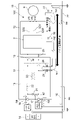
- the portion indicated by the broken line shown by 41 in the figure is a noise source composed of each switching element 3 to 8 (indicated by a switching symbol), and 42 is the inductance of the positive electrode side path 16 branched into each phase (also has an inductance). (Meaning that it becomes dominant), 43 is the inductance of the PCB pattern (which also means that the inductance becomes dominant). 44 is a parasitic capacitance between the collectors of the upper arm switching elements 3 to 5 and the housing 15, and 46 is a parasitic capacitance between the collectors of the lower arm switching elements 6 to 8 and the housing 15 (these are also dominated by the parasitic capacitance). Meaning to be).
- Reference numeral 48 is a parasitic capacitance between the emitters of the upper arm switching elements 3 to 5 and the housing 15 + a parasitic capacitance between the bus bar and the housing 15 (which also means that the parasitic capacitance is dominant).
- Reference numeral 49 is a parasitic capacitance between the emitters of the lower arm switching elements 6 to 8 and the housing 15 (which also means that the parasitic capacitance is dominant).
- the intermediate impedance Zm in the figure indicates the intermediate impedance.
- the intermediate impedance Zm includes the collectors and emitters of the upper and lower arm switching elements 3 to 8, the bus bar of the bus bar assembly 12, the winding of the motor M, and the intermediate paths 31U to include the parasitic capacitances 37, 43, 46, 48 and the parasitic inductance 47. It is a parasitic component between 31W (the midpoint between the upper arm switching elements 3 to 5 and the lower arm switching elements 6 to 8) and the housing 15, and a common mode current flows out to the housing 15 through this intermediate impedance Zm. Common mode noise will be generated.
- intermediate additional impedance Zm1 is not shown in FIG. 3, in the present invention, as shown in the embodiment of FIG. 1, the output paths 32U to 32W between the intermediate paths 31U to 31W and the motor M are normal.
- An intermediate additional impedance Zm1 composed of a mode coil 30, a three-phase common mode coil 28, and a ferrite core 29 is additionally connected, and the value of the intermediate impedance Zm is increased by that amount.
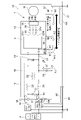
- the bridge circuit of FIG. 4 is, for example, a common mode equivalent circuit (modeled bridge circuit) when the U-phase inverter 38U in FIG. 2 becomes the noise source V1 (when the upper arm switching element 3 becomes the noise source).
- Zv is the inductance of the positive path 16 described above
- Zg is the inductance of the negative path
- Zt is the parasitic capacitance generation point P on the positive side including the capacitance of the capacitor 33
- the housing 15 reference potential conductor
- the capacitance and Zb are the capacitance between the parasitic capacitance generation point N on the negative side including the capacitance of the capacitor 34 and the housing 15, and Zm is the intermediate impedance including the intermediate additional impedance Zm1.
- the noise source is located below the intersection with the intermediate impedance Zm.
- the parasitic capacitance generation point P on the positive electrode side in the present invention is the intersection of the collector of the upper arm switching element 3 and the path 16 on the positive electrode side, and the parasitic capacitance generation point N on the negative electrode side is the lower arm switching element 6. It is the intersection of the emitter and the negative electrode side path 17 of the above.
- the inductance Zv of the positive electrode side path 16 in the present invention is the inductance of the positive electrode side path 16 to the intersection with the collector of the upper arm switching element 3, and the inductance Zg of the negative electrode side path 17 is the lower arm switching. It is the inductance of the negative electrode side path 17 to the intersection of the element 6 with the emitter.
- the intersection of the collector of the upper arm switching element 4 and the positive electrode side path 16 becomes the parasitic capacitance generation point P on the positive electrode side, and the emitter of the lower arm switching element 7.
- the intersection of the negative electrode side paths 17 is the parasitic capacitance generation point N on the negative electrode side.
- the inductance of the positive electrode side path 16 to the intersection of the upper arm switching element 4 with the collector is Zv
- the inductance of the negative electrode side path 17 to the intersection of the lower arm switching element 7 with the emitter is Zg.
- the intersection of the collector of the upper arm switching element 5 and the positive electrode side path 16 becomes the parasitic capacitance generation point P on the positive electrode side
- the emitter and the negative electrode side of the lower arm switching element 8 The intersection of the paths 17 is the parasitic capacitance generation point N on the negative electrode side.
- the inductance of the positive electrode side path 16 to the intersection of the upper arm switching element 5 with the collector is Zv
- the inductance of the negative electrode side path 17 to the intersection of the lower arm switching element 8 with the emitter is Zg.
- Z1 represents the internal impedance + inductance 42 of the upper arm of the noise source V1 (FIG. 3), and Z2 represents the internal impedance + inductance 42 of the lower arm of the noise source V1. Since the inductance 42 is minute and the connection position between the capacitor 33 and the parasitic capacitance 44 is substantially the same, the parasitic capacitance 44 is not Z1 but the capacitance Zt. Further, Zr represents the common mode impedance from the intersection of the inductance Zv and the inductance Zg (the starting point on the left side of the bridge circuit in FIG. 4) to the housing 15. The intersection of the inductance Zv and the inductance Zg in FIG. 4 is a starting point on the battery 14 (power supply) side and is a high frequency short circuit point.
- Vc is a common mode voltage generated on the LISN side which is a noise measurement point. Due to the common mode voltage Vc generated by the switching operation inside the circuit, a common mode current flows through the connected wiring, and noise is generated. By establishing an equilibrium condition (impedance balance condition) that makes the common mode voltage Vc zero or extremely small, it is possible to eliminate or significantly reduce the noise due to the common mode current that flows out due to the switching operation. ..
- the common mode voltage Vc can be expressed by the following equation (I).
- the impedance Z1 is in the ON state of the upper arm switching element 3 and is ignored because the value is lower than that of other elements.
- the parasitic capacitance generation point P on the positive electrode side and the housing 15 are located.
- the power conversion device 1 is designed so that the above equation (III) is established or substantially established by adjusting the capacitance Zt, the parasitic capacitance generation point N on the negative electrode side, and the capacitance Zb between the housing 15.
- the ratio of the inductance Zv to the inductance Zg is 1: 1 and the original parasitic capacitance between the parasitic capacitance generation point P on the positive electrode side and the housing 15 is 100 pF, 900 pF as a component of the capacitance Zt.
- a capacitor 33 additional capacitance on the positive electrode side
- a capacitor 34 additional capacitance on the negative electrode side
- the ratio of the capacitance Zt to the capacitance Zb becomes 1: 1 and the impedance balance. The conditions will be met.
- the ratio of the capacitance Zt to the capacitance Zb is approximately 1. Since it is 1, the impedance balance condition is satisfied.
- the intermediate additional impedance Zm1 (normal mode coil 30, three-phase common mode coil 28, and ferrite core 29) is connected between the intermediate paths 31U to 31W and the motor M, the drive target is Despite being a three-phase motor M, the impedance of the path passing through the parasitic capacitance 37 is sufficiently large.
- the value related to the intermediate impedance Zm that is, the molecular second term and the denominator second term of the formula (I) become negligibly small, so that the parasitic capacitance on the positive electrode side is negligible.
- the intermediate additional impedance Zm1 (normal mode coil 30, three-phase common mode coil 28, and ferrite core 29) is additionally connected between the intermediate paths 31U to 31W and the motor M.
- the impedance of the path passing through the parasitic capacitance 37 will increase, and the common mode current flowing out from this path can be reduced.
- the effect of impedance balance can be improved, and noise can be further suppressed without mounting a large EMI filter. It will be like.
- the intermediate additional impedance Zm1 is composed of a normal mode coil 30, a three-phase common mode coil 28, and a ferrite core 29.
- the common mode impedance can be increased and the outflow of the common mode current can be reduced.
- the normal mode coil 30 as the intermediate additional impedance Zm1
- the normal mode coil 30 does not require the coupling of three-phase wires, so that it can be arranged separately, and it is also arranged when it is arranged in the bus bar assembly 12 as in the embodiment. There are few restrictions on the above, and it is easier to miniaturize than in the case of a common mode coil.
- the normal mode coil 30 may not be inserted in all of the output paths 32U to 32W (three-phase) as in the embodiment, but may be inserted in only two phases, for example. This also has the advantage of being easy to use because the noise reduction effect can be obtained.
- the EMI filter 18 with the normal mode coils 22 and 35 connected to the positive electrode side path 16 and the negative electrode side path 17, respectively, as in the embodiment, the normal mode current flows out to the housing 15 as the common mode current. Inconvenience can be suppressed.
- the impedances on the positive electrode side and the negative electrode side can be made equal and the degree of equilibrium can be maintained, and the impedance balance can be maintained. It is possible to maximize the effect of.
- the equilibrium degree can be maintained even when the normal mode coil is not connected to either the positive electrode side path 16 or the negative electrode side path 17, but in that case, the normal mode current flows out as the common mode current. The inconvenience cannot be suppressed.
- FIG. 5 shows an electric circuit diagram of a power conversion device 100 without the above-mentioned normal mode coil 30, three-phase common mode coil 28, ferrite core 29, and capacitors 33 and 34.
- those shown by the same reference numerals as those in FIG. 1 are assumed to have the same or similar functions.
- the arrow indicated by N1 is the common mode current (noise) flowing out from the motor M to the housing 15 via the parasitic capacitance 37
- the arrow indicated by N2 is from the inverter circuit 2 to the housing 15 via the parasitic capacitor 36.
- the outflowing common mode current (noise), the arrow indicated by N3, indicates the common mode current (noise) flowing back from the housing 15 to the upper and lower arm switching elements 3 to 8 of the inverter circuit 2 via the Y capacitors 24 and 26, N9.
- the arrows indicate the common mode currents (noise) flowing into the LISNs 16 and 17 on the positive electrode side (+) and the negative electrode side ( ⁇ ) through the shielded wire of the HV connector attached to the housing 15, respectively.
- the arrow indicated by N4 is the common mode current (noise) flowing out from the housing 15 to the vehicle body 27, and the arrows indicated by N5 to N8 are the common mode current flowing from the vehicle body 27 to the EMI filter 18 via LISN17 and LISN16. (Noise) is shown. Although the arrows in the figure are shown in only one direction, the flow of the common mode current is not simple in reality, and the current flows in and out in both directions at each location.
- the common mode current (N1) flowing out from the motor M via the parasitic capacitance 37 becomes large. Further, the common mode current and the common mode current (N2) flowing out from the inverter circuit 2 to the housing 15 are returned to the upper and lower arm switching elements 3 to 8 of the inverter circuit 2 which is a noise source via the Y capacitors 24 and 26.
- the Y capacitors 24 and 26 are separated from the motor M and the inverter circuit 2 (N3), the recirculation path becomes long, and the filter effect of the Y capacitors 24 and 26 (the effect of recirculating the common mode current) is sufficiently obtained. I can't.
- the capacitors 33 and 34 are connected to balance the impedance, and the common mode voltage Vc is set to zero or extremely small, so that the common mode current (N1) is suppressed. , Noise can be eliminated or significantly reduced.
- the intermediate additional impedance Zm1 normal mode coil 30, three-phase common mode coil 28, and ferrite core 29
- the parasitic capacitance 37 The impedance of the path passing through is sufficiently large.
- the impedance balance (balance) is taken, the values related to the intermediate impedance Zm (the second term of the molecule and the second term of the denominator of the formula (I)) become so small that they can be ignored, so that the parasitic capacitance on the positive electrode side is generated.
- the bus bar assembly 12 is provided at a position closer to the upper and lower arm switching elements 3 to 8 of the motor M and the inverter circuit 2 than the filter substrate 13, arranging these capacitors 33 and 34 in the bus bar assembly 12 shortens the return path. , It becomes possible to obtain a high filter effect in the capacitors 33 and 34. As a result, it is possible to suppress noise without inserting a large common mode coil into the power input unit as in the conventional case, and it is possible to effectively suppress noise while reducing the size.
- the normal mode coil 30, the three-phase common mode coil 28, and the ferrite core 29 are arranged in the bus bar assembly 12 between the upper and lower arm switching elements 3 to 8 of the inverter circuit 2 and the motor M, so that the parasitic capacitance 37 is provided.
- the impedance of the path passing through the above increases, and the common mode current (noise, indicated by the arrow N1) flowing out through the parasitic capacitance 37 decreases. This also eliminates the need to insert a large common mode coil into the power input unit, and it is possible to effectively suppress noise while reducing the size of the inverter-integrated electric compressor 1.
- the capacitor 33 is connected between the positive electrode side path 16 and the housing 15 as the positive electrode side additional capacity
- the capacitor 34 is also connected between the negative electrode side path 17 and the housing 15 as the negative electrode side additional capacity. Adjust the capacitance Zt between the parasitic capacitance generation point P on the positive electrode side and the housing 15 (reference potential conductor) and the capacitance Zb between the parasitic capacitance generation point N on the negative electrode side and the housing 15 to balance the impedance.
- only one of the capacitors 33 and 34 may be connected, and the capacitance of the other (Zb or Zt) may be dealt with by adjusting the parasitic capacitance between the housings 15.
- the ratio of the inductance Zv to the inductance Zg is 1: 1 and the original parasitic capacitance between the parasitic capacitance generation point P on the positive electrode side and the housing 15 is 100 pF, this is regarded as the capacitance Zt.
- the ratio of the capacitance Zt to the capacitance Zb becomes 1: 1 and the impedance balance condition is satisfied. ..
- the capacitance between the parasitic capacitance generation point P on the positive electrode side and the housing 15 is not connected to the capacitor 33 (additional capacitance on the positive electrode side) and the capacitor 34 (additional capacitance on the negative electrode side).
- Both Zt and the parasitic capacitance generation point N on the negative electrode side and the capacitance Zb between the housings 15 may be dealt with only by adjusting the parasitic capacitance, and the impedance balance may be achieved.
- the parasitic capacitance can be adjusted, for example, by changing the distance between the heat sink and the heat sink that dissipate heat from each switching element 3 to 8, the parasitic coupling between the collector and the heat sink, and the parasitic coupling between the emitter and the heat sink. This can be done by selecting switching elements with different couplings.
- the capacitance Zt changes (adjustment).
- the switching element itself can be changed (adjusted) by the value and position of internal impedance + parasitic capacitance. If the internal impedance changes, Z1 and Z2 in FIG. 4 change, but since Z1 and Z2 are not dominant factors in the impedance balance, only the parasitic capacitance 44 changes.
- the bus bar assembly 12 in which the bus bar is molded with a hard resin is adopted as the wiring member, but in the inventions of claims 1 to 6, the bus bar may not be molded with the resin.
- the normal mode coil 30, the three-phase common mode coil 28, and the ferrite core 29 are connected as the intermediate additional impedance Zm1, but the present invention is not limited to this, and only one of them or one of them is used. Two combinations (a combination of a normal mode coil 30 and a three-phase common mode coil 28, a combination of a normal mode coil 30 and a ferrite core 29, or a combination of a three-phase common mode coil 28 and a ferrite core 29) are connected.
- the intermediate additional impedance Zm1 may be used.
- the normal mode coils 22 and 35 are connected to both the positive electrode side path 16 and the negative electrode side path 17, but in inventions other than claim 8, either the positive electrode side path 16 or the negative electrode side path 17 is connected.
- the normal mode coil (22 or 35) may be connected only to.
- the present invention is not limited to this, and the present invention is effective for various devices for driving a three-phase motor. Needless to say, there is.
Landscapes
- Engineering & Computer Science (AREA)
- Power Engineering (AREA)
- Physics & Mathematics (AREA)
- Electromagnetism (AREA)
- Inverter Devices (AREA)
Abstract
Description
実施例の電力変換装置1は、三相のインバータ回路2の各相の上下アームを構成するIGBT(MOSFETでもよい)から成る6個のスイッチング素子3~8と(図2)、プリント配線に制御回路が実装された制御基板11(図2)と、後述するバッテリ14、制御基板11、各スイッチング素子3~8、及び、モータM間の配線を行うための配線部材としてのバスバーアセンブリ12と、フィルタ基板13を備え、直流電源としての車両の前記バッテリ14から給電される直流電力を三相交流電力に変換して、モータMのステータコイル(図示せず)に給電するものである。
先ず、図1を用いて実施例の電力変換装置1の電気回路を説明する。16はバッテリ14の正極側(+)にLISN(疑似電源回路網)を介して接続された正極側経路、17はバッテリ14の負極側(-)にLISNを介して接続された負極側経路であり、これら正極側経路16と負極側経路17にはEMIフィルタ18と平滑コンデンサ19が接続されている。これらEMIフィルタ18と平滑コンデンサ19はバッテリ14とインバータ回路2のスイッチング素子3~8の間に接続されている。
また、平滑コンデンサ19の後段の正極側経路16及び負極側経路17にはインバータ回路2が接続されており、インバータ回路2の後述する中間経路31U~31WとモータMの間には、本発明における中間付加インピーダンスZm1を構成するノーマルモードコイル30、三相コモンモードコイル28、及び、フェライトコア29が順次接続されている。これらノーマルモードコイル30や三相コモンモードコイル28は主に低周波のインピーダンスを増加させ、フェライトコア29は高周波のインピーダンスを増加させる。フェライトコア29は後述する出力経路32U~32Wの周囲に配置するものであるが、本発明では係る配置も接続と称する。また、ノーマルモードコイル30は実施例では出力経路32U~32Wの全てにそれぞれ接続されているものとする。
更に、インバータ回路2と平滑コンデンサ19の間の正極側経路16と筐体15(基準電位導体)間には、実施例では正極側の寄生容量発生ポイントPと筐体15間の容量Ztを構成する正極側付加容量としてのコンデンサ33(インピーダンスバランス用)を接続し、インバータ回路2と平滑コンデンサ19の間の負極側経路17と筐体15(基準電位導体)間には、実施例では負極側の寄生容量発生ポイントNと筐体15間の容量Zbを構成する負極側付加容量としてのコンデンサ34(インピーダンスバランス用)を接続している。尚、図1では寄生容量発生ポイントP、Nと離れてコンデンサ33、34を示しているが、実際には図3に示すように、コンデンサ33(正極側付加容量)は正極側の寄生容量発生ポイントP(上アームスイッチング素子3~5のコレクタと正極側経路16の交点)と筐体15間に接続され、コンデンサ34(負極側付加容量)は実施例ではシャント抵抗25を介し、負極側の寄生容量発生ポイントN(下アームスイッチング素子6~8のエミッタと負極側経路17の交点)と筐体15間に接続されている。また、シャント抵抗25の位置も、図1では分かりやすくするために負極側の寄生容量発生ポイントNから離して示している。
次に、図2にはインバータ回路2の電気回路と制御基板11を示している。インバータ回路2は、U相インバータ38U、V相インバータ38V、W相インバータ38Wを有しており、各相インバータ38U~38Wは、それぞれ前述した上アーム側のスイッチング素子(上アームスイッチング素子と称す)3~5と、下アーム側のスイッチング素子(下アームスイッチング素子と称す)6~8を個別に有している。更に、各スイッチング素子3~8には、それぞれフライホイールダイオード39が逆並列に接続されている。
一方、制御基板11の制御回路はプロセッサを有するマイクロコンピュータから構成されており、実施例では車両のECUから回転数指令値を入力し、シャント抵抗25を用いてモータMの相電流を検出及び算出し、これらに基づき、インバータ回路2の各上下アームスイッチング素子3~8のON/OFF状態を制御する。具体的には、各上下アームスイッチング素子3~8のゲート端子に印加するゲート電圧(駆動信号)を制御し、各相の上下アームスイッチング素子3~8をそれぞれ接続する中間経路31U~31Wの電圧(相電圧)を三相交流出力とし、出力経路32U~32Wを介してモータMの各相のステータコイルに印加することで当該モータMを駆動する。
また、実施例のバスバーアセンブリ12は、導電性金属から成るバスバーを硬質樹脂によりモールドした構成とされている。このバスバーアセンブリ12のバスバーにフィルタ基板13や制御基板11、各スイッチング素子3~8、モータMが接続されることで、バッテリ14、制御基板11、各スイッチング素子3~8、モータM間の配線が成される。
次に、図3を用いて、電力変換装置1の制御基板11(バスバーアセンブリ12を含む)の寄生成分について説明する。図中Zvはバスバーアセンブリ12を含む正極側経路16(配線)のインダクタンス、Zgはバスバーアセンブリ12を含む負極側経路17(配線)のインダクタンスである。正極側経路16や負極側経路17には他の寄生成分も存在するが、配線のインダクタンスが支配的となる。
次に、図4を参照しながら、インピーダンスバランス条件(平衡条件)を成立させることによるノイズの低減対策について説明する。図4のブリッジ回路は例えば図2中のU相インバータ38Uがノイズ源V1となるとき(上アームスイッチング素子3がノイズ源となる際)のコモンモード等価回路(モデル化されたブリッジ回路)であり、図中Zvは前述した正極側経路16のインダクタンス、Zgは負極側経路17のインダクタンス、Ztはコンデンサ33の容量を含む正極側の寄生容量発生ポイントPと筐体15(基準電位導体)間の容量、Zbはコンデンサ34の容量を含む負極側の寄生容量発生ポイントNと筐体15間の容量、Zmは中間付加インピーダンスZm1を含む中間インピーダンスである。下アームスイッチング素子6がノイズ源となる際は、ノイズ源は中間インピーダンスZmとの交点の下側に位置することになる。


Zg・Zt=Zb・Zv ・・・(III)
次に、図5、図6を参照しながら、本発明によるノイズ低減効果について説明する。図5は前述したノーマルモードコイル30、三相コモンモードコイル28、フェライトコア29、コンデンサ33、34を設けない電力変換装置100の電気回路図を示している。尚、この図において図1と同一符号で示すものは同一若しくは同様の機能を奏するものとする。
2 インバータ回路
3~8 上下アームスイッチング素子
11 制御基板
12 バスバーアセンブリ(配線部材)
14 バッテリ(直流電源)
15 筐体(基準電位導体)
16 正極側経路
17 負極側経路
22、35 ノーマルモードコイル
28 三相コモンモードコイル(Zm1)
29 フェライトコア(Zm1)
30 ノーマルモードコイル(Zm1)
31U~31W 中間経路
32U~32W 出力経路
33 コンデンサ(正極側付加容量)
34 コンデンサ(負極側付加容量)
M モータ
N 負極側の寄生容量発生ポイント
P 正極側の寄生容量発生ポイント
Zb 負極側の寄生容量発生ポイントNと筐体15間の容量
Zg 負極側経路のインダクタンス
Zm 中間インピーダンス
Zm1 中間付加インピーダンス
Zt 正極側の寄生容量発生ポイントPと筐体15間の容量
Zv 正極側経路のインダクタンス
Claims (8)
- 各相の上アームスイッチング素子と下アームスイッチング素子を有して三相交流出力をモータに印加する電力変換装置において、
直流電源の正極側と前記上アームスイッチング素子の高電位側端子とを接続する正極側経路と、
前記直流電源の負極側と前記下アームスイッチング素子の低電位側端子とを接続する負極側経路と、
前記上アームスイッチング素子の低電位側端子と前記下アームスイッチング素子の高電位側端子とを接続する中間経路とを備え、
前記正極側経路のインダクタンスをZv、前記負極側経路のインダクタンスをZg、正極側の寄生容量発生ポイントPと基準電位導体間の容量をZt、負極側の寄生容量発生ポイントNと前記基準電位導体間の容量をZbとしたとき、前記正極側経路のインダクタンスZv、前記負極側経路のインダクタンスZg、前記正極側の寄生容量発生ポイントPと前記基準電位導体間の容量Zt、及び、前記負極側の寄生容量発生ポイントNと前記基準電位導体間の容量Zbで構成されるブリッジ回路の平衡条件に基づき、前記正極側の寄生容量発生ポイントPと前記基準電位導体間の容量Zt、及び、前記負極側の寄生容量発生ポイントNと前記基準電位導体間の容量Zbが設定されると共に、
前記中間経路と前記モータとの間には中間付加インピーダンスZm1が接続されていることを特徴とする電力変換装置。 - Zg・Zt=Zb・Zvの関係が成立し、若しくは、Zg・Zt=Zb・Zvの関係が略成立することを特徴とする請求項1に記載の電力変換装置。
- 前記正極側の寄生容量発生ポイントPと前記基準電位導体との間に接続された正極側付加容量と、前記負極側の寄生容量発生ポイントNと前記基準電位導体との間に接続された負極側付加容量、のうちの何れか一方、又は、双方を備えたことを特徴とする請求項1又は請求項2に記載の電力変換装置。
- 前記中間付加インピーダンスZm1は、ノーマルモードコイル、三相コモンモードコイル、フェライトコアのうちの何れか、又は、それらのうちの二つの組み合わせ、若しくは、それらの全てにより構成されていることを特徴とする請求項1乃至請求項3のうちの何れかに記載の電力変換装置。
- 前記上下アームスイッチング素子のスイッチングを制御する制御基板と、
前記直流電源、前記制御基板、前記上下アームスイッチング素子、及び、前記モータ間の配線を行うために設けられた配線部材とを備え、
前記中間付加インピーダンスZm1を、前記配線部材に配置したことを特徴とする請求項1乃至請求項4のうちの何れかに記載の電力変換装置。 - 前記正極側の寄生容量発生ポイントPと前記基準電位導体との間に接続された正極側付加容量と、前記負極側の寄生容量発生ポイントNと前記基準電位導体との間に接続された負極側付加容量、のうちの何れか一方、又は、双方を備え、
前記正極側付加容量、及び/又は、前記負極側付加容量を、前記配線部材に配置したことを特徴とする請求項5に記載の電力変換装置。 - 前記配線部材は、バスバーを樹脂モールドして成るバスバーアセンブリであることを特徴とする請求項5又は請求項6に記載の電力変換装置。
- 前記直流電源と前記上下アームスイッチング素子の間に接続されたEMIフィルタを備え、
該EMIフィルタは、前記正極側経路と前記負極側経路の双方にそれぞれ接続されたノーマルモードコイルを備えたことを特徴とする請求項1乃至請求項7のうちの何れかに記載の電力変換装置。
Priority Applications (4)
| Application Number | Priority Date | Filing Date | Title |
|---|---|---|---|
| US18/035,012 US12431829B2 (en) | 2020-11-19 | 2021-11-17 | Power conversion device |
| DE112021004774.4T DE112021004774T5 (de) | 2020-11-19 | 2021-11-17 | Stromumwandlungsvorrichtung |
| JP2022563800A JP7496434B2 (ja) | 2020-11-19 | 2021-11-17 | 電力変換装置 |
| CN202180076574.5A CN116530005A (zh) | 2020-11-19 | 2021-11-17 | 功率转换装置 |
Applications Claiming Priority (2)
| Application Number | Priority Date | Filing Date | Title |
|---|---|---|---|
| JP2020192123 | 2020-11-19 | ||
| JP2020-192123 | 2020-11-19 |
Publications (1)
| Publication Number | Publication Date |
|---|---|
| WO2022107809A1 true WO2022107809A1 (ja) | 2022-05-27 |
Family
ID=81708940
Family Applications (1)
| Application Number | Title | Priority Date | Filing Date |
|---|---|---|---|
| PCT/JP2021/042240 Ceased WO2022107809A1 (ja) | 2020-11-19 | 2021-11-17 | 電力変換装置 |
Country Status (5)
| Country | Link |
|---|---|
| US (1) | US12431829B2 (ja) |
| JP (1) | JP7496434B2 (ja) |
| CN (1) | CN116530005A (ja) |
| DE (1) | DE112021004774T5 (ja) |
| WO (1) | WO2022107809A1 (ja) |
Cited By (3)
| Publication number | Priority date | Publication date | Assignee | Title |
|---|---|---|---|---|
| WO2023090263A1 (ja) * | 2021-11-17 | 2023-05-25 | サンデン株式会社 | 電力変換装置及びその製造方法 |
| WO2024024355A1 (ja) * | 2022-07-27 | 2024-02-01 | サンデン株式会社 | コモンモードコイル、インバータ装置及び電動圧縮機 |
| JP2024145976A (ja) * | 2023-03-31 | 2024-10-15 | ダイキン工業株式会社 | 電力変換装置、空気調和機 |
Families Citing this family (1)
| Publication number | Priority date | Publication date | Assignee | Title |
|---|---|---|---|---|
| EP4575223A1 (en) * | 2023-12-19 | 2025-06-25 | Nordex Energy SE & Co. KG | System for a wind turbine and wind turbine |
Citations (3)
| Publication number | Priority date | Publication date | Assignee | Title |
|---|---|---|---|---|
| JP2009273272A (ja) * | 2008-05-08 | 2009-11-19 | Toyota Motor Corp | インバータモジュール |
| JP2017163709A (ja) * | 2016-03-09 | 2017-09-14 | 株式会社豊田中央研究所 | 三相インバータ及び三相インバータ用の半導体モジュール |
| JP2020167787A (ja) * | 2019-03-28 | 2020-10-08 | 株式会社デンソー | 電力変換装置 |
Family Cites Families (12)
| Publication number | Priority date | Publication date | Assignee | Title |
|---|---|---|---|---|
| JPS5091521U (ja) | 1973-12-20 | 1975-08-01 | ||
| US5517063A (en) * | 1994-06-10 | 1996-05-14 | Westinghouse Electric Corp. | Three phase power bridge assembly |
| US5852558A (en) * | 1997-06-20 | 1998-12-22 | Wisconsin Alumni Research Foundation | Method and apparatus for reducing common mode voltage in multi-phase power converters |
| US6342793B1 (en) * | 1999-11-03 | 2002-01-29 | International Business Machines Corporation | Method and system for sending large numbers of CMOS control signals into a separate quiet analog power domain |
| US6926288B2 (en) * | 2003-06-02 | 2005-08-09 | Bose Corporation | Electromagnetic interference filter |
| JP5091521B2 (ja) | 2007-03-29 | 2012-12-05 | 三菱重工業株式会社 | 一体型電動圧縮機 |
| US7787270B2 (en) * | 2007-06-06 | 2010-08-31 | General Electric Company | DC-DC and DC-AC power conversion system |
| JP5637944B2 (ja) * | 2011-06-29 | 2014-12-10 | 株式会社 日立パワーデバイス | パワー半導体モジュール |
| US9209176B2 (en) * | 2011-12-07 | 2015-12-08 | Transphorm Inc. | Semiconductor modules and methods of forming the same |
| US9374021B2 (en) * | 2013-12-16 | 2016-06-21 | Rockwell Automation Technologies, Inc. | PWM output voltage measurement apparatus and method |
| JP6425380B2 (ja) * | 2013-12-26 | 2018-11-21 | ローム株式会社 | パワー回路およびパワーモジュール |
| JP7011539B2 (ja) | 2018-06-19 | 2022-01-26 | 株式会社Soken | 電力変換装置 |
-
2021
- 2021-11-17 DE DE112021004774.4T patent/DE112021004774T5/de active Pending
- 2021-11-17 WO PCT/JP2021/042240 patent/WO2022107809A1/ja not_active Ceased
- 2021-11-17 JP JP2022563800A patent/JP7496434B2/ja active Active
- 2021-11-17 CN CN202180076574.5A patent/CN116530005A/zh active Pending
- 2021-11-17 US US18/035,012 patent/US12431829B2/en active Active
Patent Citations (3)
| Publication number | Priority date | Publication date | Assignee | Title |
|---|---|---|---|---|
| JP2009273272A (ja) * | 2008-05-08 | 2009-11-19 | Toyota Motor Corp | インバータモジュール |
| JP2017163709A (ja) * | 2016-03-09 | 2017-09-14 | 株式会社豊田中央研究所 | 三相インバータ及び三相インバータ用の半導体モジュール |
| JP2020167787A (ja) * | 2019-03-28 | 2020-10-08 | 株式会社デンソー | 電力変換装置 |
Cited By (6)
| Publication number | Priority date | Publication date | Assignee | Title |
|---|---|---|---|---|
| WO2023090263A1 (ja) * | 2021-11-17 | 2023-05-25 | サンデン株式会社 | 電力変換装置及びその製造方法 |
| JP2023074301A (ja) * | 2021-11-17 | 2023-05-29 | サンデン株式会社 | 電力変換装置及びその製造方法 |
| JP7802495B2 (ja) | 2021-11-17 | 2026-01-20 | サンデン株式会社 | 電力変換装置及びその製造方法 |
| WO2024024355A1 (ja) * | 2022-07-27 | 2024-02-01 | サンデン株式会社 | コモンモードコイル、インバータ装置及び電動圧縮機 |
| JP2024145976A (ja) * | 2023-03-31 | 2024-10-15 | ダイキン工業株式会社 | 電力変換装置、空気調和機 |
| JP7846383B2 (ja) | 2023-03-31 | 2026-04-15 | ダイキン工業株式会社 | 電力変換装置、空気調和機 |
Also Published As
| Publication number | Publication date |
|---|---|
| US20240014758A1 (en) | 2024-01-11 |
| US12431829B2 (en) | 2025-09-30 |
| DE112021004774T5 (de) | 2023-10-26 |
| JP7496434B2 (ja) | 2024-06-06 |
| CN116530005A (zh) | 2023-08-01 |
| JPWO2022107809A1 (ja) | 2022-05-27 |
Similar Documents
| Publication | Publication Date | Title |
|---|---|---|
| JP7496434B2 (ja) | 電力変換装置 | |
| EP2398136B1 (en) | Inverter device and inverter-integrated electric compressor | |
| CN103765750B (zh) | 电力变换装置 | |
| JP6980630B2 (ja) | 高電圧フィルタおよび電力変換装置 | |
| WO2015049774A1 (ja) | 電力変換装置 | |
| JP7523575B2 (ja) | インバータ一体型電動圧縮機 | |
| WO2021152888A1 (ja) | ノイズフィルタ、ノイズフィルタ装置、および電力変換装置 | |
| CN115516762B (zh) | 滤波装置及电力变换装置 | |
| JP2007082359A (ja) | インバータ装置および制御装置 | |
| JP5385939B2 (ja) | 電動機駆動システム | |
| JP5203737B2 (ja) | 車両駆動装置 | |
| JP7802495B2 (ja) | 電力変換装置及びその製造方法 | |
| JP7678642B2 (ja) | フィルタ装置及び電力変換装置 | |
| CN118525443A (zh) | 半导体装置和具备半导体装置的逆变器 | |
| JP2013099001A (ja) | スイッチング素子装置 | |
| JP7506522B2 (ja) | ノイズフィルタ、電力変換装置 | |
| CN222868800U (zh) | 功率模块、电子设备、电机控制器及车辆 | |
| CN212660104U (zh) | 驱动器的电磁干扰抑制装置及驱动器 | |
| CN110391755A (zh) | 电路基板 | |
| CN219938234U (zh) | 一种24v三相风机的emc优化电路 | |
| JP2015228748A (ja) | モータシステム | |
| US20260128677A1 (en) | Power converter with coupled inductors | |
| JP2026052346A (ja) | コモンモードノイズフィルター | |
| JP2024164828A (ja) | 電力変換装置 | |
| JP2023137607A (ja) | 電力変換装置 |
Legal Events
| Date | Code | Title | Description |
|---|---|---|---|
| 121 | Ep: the epo has been informed by wipo that ep was designated in this application |
Ref document number: 21894683 Country of ref document: EP Kind code of ref document: A1 |
|
| ENP | Entry into the national phase |
Ref document number: 2022563800 Country of ref document: JP Kind code of ref document: A |
|
| WWE | Wipo information: entry into national phase |
Ref document number: 18035012 Country of ref document: US |
|
| WWE | Wipo information: entry into national phase |
Ref document number: 112021004774 Country of ref document: DE |
|
| WWE | Wipo information: entry into national phase |
Ref document number: 202180076574.5 Country of ref document: CN |
|
| 122 | Ep: pct application non-entry in european phase |
Ref document number: 21894683 Country of ref document: EP Kind code of ref document: A1 |
|
| WWG | Wipo information: grant in national office |
Ref document number: 18035012 Country of ref document: US |