WO2022102743A1 - カバー - Google Patents
カバー Download PDFInfo
- Publication number
- WO2022102743A1 WO2022102743A1 PCT/JP2021/041711 JP2021041711W WO2022102743A1 WO 2022102743 A1 WO2022102743 A1 WO 2022102743A1 JP 2021041711 W JP2021041711 W JP 2021041711W WO 2022102743 A1 WO2022102743 A1 WO 2022102743A1
- Authority
- WO
- WIPO (PCT)
- Prior art keywords
- cover
- conductor
- area
- radio wave
- main body
- Prior art date
- Legal status (The legal status is an assumption and is not a legal conclusion. Google has not performed a legal analysis and makes no representation as to the accuracy of the status listed.)
- Ceased
Links
Images








Classifications
-
- F—MECHANICAL ENGINEERING; LIGHTING; HEATING; WEAPONS; BLASTING
- F21—LIGHTING
- F21S—NON-PORTABLE LIGHTING DEVICES; SYSTEMS THEREOF; VEHICLE LIGHTING DEVICES SPECIALLY ADAPTED FOR VEHICLE EXTERIORS
- F21S45/00—Arrangements within vehicle lighting devices specially adapted for vehicle exteriors, for purposes other than emission or distribution of light
- F21S45/60—Heating of lighting devices, e.g. for demisting
-
- H—ELECTRICITY
- H05—ELECTRIC TECHNIQUES NOT OTHERWISE PROVIDED FOR
- H05B—ELECTRIC HEATING; ELECTRIC LIGHT SOURCES NOT OTHERWISE PROVIDED FOR; CIRCUIT ARRANGEMENTS FOR ELECTRIC LIGHT SOURCES, IN GENERAL
- H05B3/00—Ohmic-resistance heating
- H05B3/10—Heating elements characterised by the composition or nature of the materials or by the arrangement of the conductor
- H05B3/18—Heating elements characterised by the composition or nature of the materials or by the arrangement of the conductor the conductor being embedded in an insulating material
-
- F—MECHANICAL ENGINEERING; LIGHTING; HEATING; WEAPONS; BLASTING
- F21—LIGHTING
- F21W—INDEXING SCHEME ASSOCIATED WITH SUBCLASSES F21K, F21L, F21S and F21V, RELATING TO USES OR APPLICATIONS OF LIGHTING DEVICES OR SYSTEMS
- F21W2102/00—Exterior vehicle lighting devices for illuminating purposes
- F21W2102/10—Arrangement or contour of the emitted light
-
- F—MECHANICAL ENGINEERING; LIGHTING; HEATING; WEAPONS; BLASTING
- F21—LIGHTING
- F21W—INDEXING SCHEME ASSOCIATED WITH SUBCLASSES F21K, F21L, F21S and F21V, RELATING TO USES OR APPLICATIONS OF LIGHTING DEVICES OR SYSTEMS
- F21W2103/00—Exterior vehicle lighting devices for signalling purposes
Definitions
- the present invention relates to a cover.
- Moving objects such as automobiles are equipped with lighting that brings light to the outside, such as headlights and tail lamps.
- lighting has a light source and a cover.
- a moving object such as a car may be equipped with a radio wave device for detecting external obstacles.
- the radio wave device transmits radio waves such as millimeter waves to the outside and receives radio waves reflected from the outside.
- the radio wave device can detect the position and size of an external obstacle from the difference between the transmitted radio wave and the received radio wave.
- a radio wave device is covered with a cover together with a light source, a problem has been discovered that the radio wave may be blocked by the cover having a conductor and the radio wave device may not function.
- the first cover of the present invention is a cover arranged so as to face the light source and the radio wave device that transmits and / or receives radio waves.
- the cover body and A conductor provided on the cover main body is provided.
- the cover main body has light transmission and radio wave transmission, and has
- the cover main body portion includes a first area facing the radio wave device and a second area facing the light source.
- the conductor generates heat when a voltage is applied,
- the conductor includes a plurality of conductive portions arranged at intervals. The plurality of conductive portions located in the first area are arranged at the first interval.
- the first interval may be 900 nm or more and 100 mm or less.
- the plurality of conductive portions located in the first area may extend in the same direction.
- the direction in which the plurality of conductive portions located in the first area extend may be at an angle of 45 ° or more with respect to the plane of polarization of the radio wave.
- the width of the conductive portion may be 50 ⁇ m or less.
- the plurality of conductive portions located in the second area may be arranged at a second interval.
- the second area may be located away from the intersection of the optical axis of the light source and the cover main body.
- the second interval may be smaller than the first interval.
- the second interval may be larger than the first interval.
- the light source may be an LED light source.
- the visible light transmittance of the cover may be 50% or more.
- the conductive portion may have a conductive layer and a dark color layer provided on the opposite side of the conductive layer from the light source.
- the second cover of the present invention is a cover arranged facing the light source.
- the cover body and A conductor provided on the cover main body is provided.
- the cover main body has light transmission and radio wave transmission, and has
- the cover main body portion includes a first area and a second area facing the light source.
- the conductor generates heat when a voltage is applied,
- the conductor has a plurality of conductive portions arranged at intervals, and the conductor has a plurality of conductive portions.
- the plurality of conductive portions located in the first area are arranged at the first interval.
- the third cover of the present invention is a cover arranged facing a radio wave device that transmits and / or receives radio waves.
- the cover body and A conductor provided on the cover main body is provided.
- the cover main body has light transmission and radio wave transmission, and has
- the cover main body portion includes a first area facing the radio wave device and a second area.
- the conductor generates heat when a voltage is applied,
- the conductor has a plurality of conductive portions arranged at intervals, and the conductor has a plurality of conductive portions.
- the plurality of conductive portions located in the first area are arranged at the first interval.
- the fourth cover of the present invention is a cover arranged so as to face the light source and the radio wave device that transmits and / or receives radio waves.
- the main body With a conductor provided in the main body, The main body has light transmission and radio wave transmission, and has The conductor generates heat when a voltage is applied,
- the conductor includes a plurality of conductive portions arranged at intervals.
- the conductor includes a first portion facing the radio wave device. The plurality of conductive portions in the first portion are arranged at the first interval.
- radio waves can be transmitted to a cover having a conductor.
- FIG. 1 is a diagram for explaining an embodiment according to the present invention, and is a perspective view schematically showing a moving body provided with a cover.
- FIG. 1 schematically shows an automobile provided with a cover as an example of a moving body.
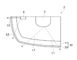
- FIG. 2 is a cross-sectional view showing a light source and a radio wave device in which a cover and a cover are arranged facing each other.
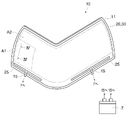
- FIG. 3 is a perspective view schematically showing the cover.
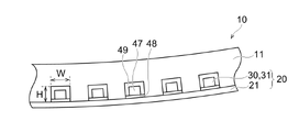
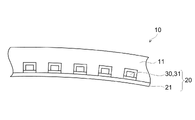
- FIG. 4 is a cross-sectional view of the cover taken along the line IV-IV of FIG.
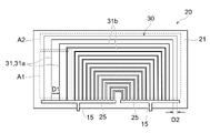
- FIG. 5 is a plan view showing the cover from the normal direction of the sheet surface, and is a plan view showing an example of the arrangement of the conductors.
- FIG. 1 is a diagram for explaining an embodiment according to the present invention, and is a perspective view schematically showing a moving body provided with a cover.
- FIG. 1 schematically shows an automobile provided with a cover as an example of a moving body.
- FIG. 2 is a cross-
- FIG. 6 is a diagram for explaining the relationship between the first portion of the conductor and the plane of polarization of the radio wave by the radio wave device.
- FIG. 7 is a diagram for explaining a method for manufacturing a conductor.
- FIG. 8 is a diagram for explaining a method for manufacturing a conductor.
- FIG. 9 is a diagram for explaining a method for manufacturing a conductor.
- FIG. 10 is a diagram for explaining a method for manufacturing a conductor.
- FIG. 11 is a diagram for explaining a method for manufacturing a conductor.
- FIG. 12 is a diagram for explaining a method of manufacturing a cover.
- FIG. 13 is a diagram for explaining an example of a method for manufacturing a cover.
- FIG. 14 is a diagram for explaining another example of the method of manufacturing the cover.
- FIG. 15 is a cross-sectional view showing a modified example of the cover.
- FIG. 16 is a diagram showing a modified example of the arrangement of conductors.
- FIG. 17
- the terms "board”, “sheet”, and “film” are not distinguished from each other based only on the difference in names.
- sheet with conductor is a concept including members that can be called a plate or a film.
- a "sheet with a conductor” cannot be distinguished from a member called a "plate with a conductor” or a "film with a conductor” only by a difference in name.
- the "seat surface” refers to a surface that coincides with the plane direction of the target sheet-shaped member when the target sheet-shaped member is viewed as a whole and from a broad perspective. The same applies when “sheet” is replaced with “board” or "film”.
- FIG. 1 is a perspective view schematically showing an automobile provided with a cover.
- FIG. 2 is a cross-sectional view showing a light source and a radio wave device in which a cover and a cover are arranged facing each other.
- the automobile 1 as an example of the moving body is provided with the lighting 2.
- the illumination 2 is the headlight of the automobile 1.
- the illumination 2 has a light source 3, a radio wave device 5, and a cover 10.
- the cover 10 forms the surface of the illumination 2.
- the light source 3 and the radio wave device 5 are arranged in the space partitioned by the cover 10.
- the cover 10 is arranged so as to face the radio wave device 5 and the light source 3, and protects the radio wave device 5 and the light source 3 from the outside.
- the light source 3 can emit a predetermined color such as white.
- the light from the light source 3 is brought to the outside of the illumination 2 by passing through the cover 10.
- the visible light transmittance of the cover 10 is preferably 50% or more, and more preferably 70% or more so that the light from the light source 3 can sufficiently pass through the cover 10.
- the light source 3 is preferably an LED light source having high luminous efficiency and long life, for example.
- the radio wave device 5 is a device that transmits and / or receives radio waves.
- the radio wave transmitted and / or received by the radio wave device 5 may have a frequency of, for example, 30 to 300 GHz, 30 to 1200 THz, or 20 kHz to 1 GHz.
- the radio wave device 5 may be applied to, for example, a radar of a collision prevention system. As shown in FIG. 1, an automobile has a power source 7 such as a battery.
- the fact that the cover 10 faces the light source 3 means that the light L1 from the light source 3 as shown in FIG. 2 is incident on the cover 10.
- the fact that the cover 10 faces the radio wave device 5 means that the radio wave L2 from the radio wave device 5 as shown in FIG. 2 is incident on the cover 10.
- FIG. 3 is a perspective view schematically showing the cover 10.
- the cover 10 is a curved plate-shaped member.
- FIG. 4 is a cross-sectional view of the cover along line IV-IV of FIG.
- the cover 10 is curved so that the side of the base material 21 described later of the sheet 20 with a conductor is on the outside.
- the cover 10 has a cover main body portion 11 and a conductor-equipped sheet 20 provided on the cover main body portion 11.
- the sheet 20 with a conductor is provided so as to form the outer surface of the cover 10.
- the cover main body 11 supports the sheet 20 with a conductor.
- the cover main body 11 is curved in a shape that matches the shape of the cover 10.
- the cover main body 11 is transparent so that the light from the light source 3 can be transmitted.
- the cover main body 11 is not limited to colorless and transparent as long as it can appropriately transmit the light from the light source 3, and may be colored and transparent by containing a coloring material such as a pigment.
- the cover main body 11 transmits radio waves transmitted and / or received by the radio wave device 5.
- the cover main body 11 has light transmission and radio wave transmission.
- the cover main body 11 may be made of, for example, a resin such as polyethylene terephthalate, polyethylene naphthalate, polycarbonate, polystyrene, or cyclic polyolefin, or thin-film glass.
- the cover main body portion 11 preferably has a thickness of 1 mm or more and 5 mm or less. With such a thickness, excellent strength and optical characteristics can be imparted to the cover main body 11.
- transparency and “light transmittance” mean that the member has transparency to the extent that one side of the member can see through the other side. It means that it has a visible light transmittance of, for example, 30% or more, more preferably 70% or more.
- Cold transparency means that the transmittance of light in a specific wavelength range is intentionally low, but the transmittance of visible light as a whole is high and transparent. Visible light transmittance is the transmittance at each wavelength when measured using a spectrophotometer (“UV-3100PC” manufactured by Shimadzu Corporation, JIS K 0115 compliant product) within the measurement wavelength range of 380 nm to 780 nm. Specified as the average value of.
- radio wave permeability means that radio waves transmitted and / or received by the radio wave device 5 can be transmitted to such an extent that the radio wave device 5 can function properly, for example, the frequency is 30. It means that radio waves of ⁇ 300 GHz, 30 to 1200 THz, or 20 kHz to 1 GHz can be transmitted by 80% or more.
- the transmittance of radio waves can be measured using a millimeter-wave / microwave transmission attenuation measurement system (“Model No. RTS01 LAF-26.5A (for 26.5-110 GHz)” manufactured by KEYCOM).
- the cover main body portion 11 includes a first area A1 and a second area A2.
- the first area A1 faces the radio wave device 5.
- the second area A2 faces the light source 3.
- the first area A1 is an area of the cover main body 11 to which the radio wave from the radio wave device 5 is incident.
- the second area A2 is an area of the cover main body 11 to which the light from the light source 3 is incident.
- the second area A2 is different from the first area A1.
- the area may be the first area A1.
- the second area A2 may be an area other than the area where the radio wave from the radio wave device 5 is incident.
- the size and arrangement of the first area A1 and the second area A2 are appropriately designed according to the arrangement of the light source 3 and the radio wave device 5 in the illumination 2.
- the sheet 20 with a conductor has substantially the same plane dimensions as the cover 10 along the sheet surface of the cover 10, and is arranged over the entire cover 10.
- the sheet 20 with a conductor has a base material 21, a conductor 30, and a pair of bus bars 25.
- the conductor 30 is provided on one surface of the base material 21.
- the pair of bus bars 25 are electrically connected to the conductor 30, and the conductor 30 can be energized by applying a voltage.
- the side where the conductor 30 is provided with respect to the base material 21 of the sheet 20 with the conductor is the side where the cover main body 11 is provided.
- the cover 10 has a wiring portion 15 for energizing the conductor 30.
- the conductor 30 is energized from the wiring portion 15 via the bus bar 25 of the sheet 20 with the conductor by the power source 7 such as a battery.
- the conductor 30 generates heat when a voltage is applied.
- the heat generated by the conductor 30 is transferred to the surface of the cover 10.
- the heat transferred to the surface of the cover 10 can remove ice and water droplets adhering to the surface of the cover 10. By removing ice and water droplets, the light from the light source 3 can be brought to the outside of the cover 10. Since the cover 10 transmits radio waves, the radio wave device 5 functions normally.
- the base material 21 is a member that supports the bus bar 25 and the conductor 30.
- the base material 21 is a transparent electrically insulating film.
- the base material 21 may be any material as long as it is transparent and can appropriately support the conductor 30.
- the material of the base material 21 may be, for example, polyethylene terephthalate, polyethylene naphthalate, polycarbonate, polystyrene, cyclic polyolefin or the like.
- the thickness of the base material 21 is preferably 30 ⁇ m or more and 500 ⁇ m or less in consideration of light transmission, appropriate support of the conductor 30, impact resistance, durability, thermal conductivity, and the like.
- the difference between the refractive index of the base material 21 and the refractive index of the cover main body 11 is small and the same. More preferred.
- the base material 21 and the cover main body 11 may be made of the same material.
- the pair of bus bars 25 are arranged apart from each other and are electrically connected to the corresponding wiring portions 15.
- the voltage of the power supply 7 connected to the wiring portion 15 is applied between the pair of bus bars 25.
- the bus bar 25 is arranged in the vicinity of the outer edge portion of the sheet 20 with a conductor.
- the pair of bus bars 25 may be arranged on the same side with respect to the conductor 30 as shown in FIG. 3 or the like as long as they are near the outer edge portion of the sheet 20 with a conductor, or may be arranged on the opposite side. It may be arranged.
- the bus bar 25 may be provided at a position not supported by the base material 21.
- the bus bar 25 may be provided at a position that is not observed from the outside of the moving body, for example, a position that overlaps with the bonnet or bumper of the automobile 1.
- FIG. 5 is a plan view of the sheet 20 with a conductor observed from the normal direction of the sheet surface.
- the curved sheet 20 with a conductor is shown in a flat plate shape.
- the conductor 30 is arranged so as to connect the pair of bus bars 25, and electrically connects the pair of bus bars 25.
- the conductor 30 generates heat when a voltage is applied via the wiring portion 15 and the bus bar 25. This heat is transferred to the surface of the cover 10 to generate heat on the surface of the cover 10.
- the conductor 30 has a plurality of conductive portions 31 arranged at intervals.
- the conductive portion 31 extends linearly.
- Each of the plurality of conductive portions 31 connects a pair of bus bars 25.
- the plurality of conductive portions 31 independently connect a pair of bus bars 25.
- the resistances of the plurality of conductive portions 31 are substantially the same so that the conductive portions 31 generate heat uniformly, in other words, the amount of heat generated per unit length in each of the conductive portions 31 is substantially the same. ..
- the plurality of conductive portions 31 include a first portion 31a located in the first zone A1 and a second portion 31b located in the second zone A2.
- the first portion 31a means a plurality of conductive portions 31 located in the first area A1.
- the second portion 31b means a plurality of conductive portions 31 located in the second area A2.
- the first portion 31a is arranged at the first interval D1.
- the second portion 31b is arranged at the second interval D2.
- the first portion 31a is connected to a portion of the second portion 31b.
- the first portion 31a connects the pair of bus bars 25 by connecting to the second portion 31b.
- the second portion 31b which is not connected to the first portion 31a, connects a pair of bus bars 25, respectively.
- the first portion 31a may connect a pair of bus bars 25 without connecting to the second portion 31b.
- the first interval D1 is appropriately set according to the wavelength of the radio wave transmitted and / or received by the radio wave device 5.
- the first spacing D1 is 900 nm or more and 100 mm or less.
- the first interval D1 is preferably 1 mm or more and 10 mm or less.
- the first interval D1 is preferably 250 nm or more and 10 ⁇ m or less.
- the frequency of the radio wave is an ultrasonic wave such as 20 kHz to 1 GHz
- the first interval D1 is preferably 0.34 ⁇ m or more and 17 mm or less. In the example shown in FIG.
- the first interval D1 is the same.
- the first interval D1 may be different from each other.
- the first interval D1 may change regularly or irregularly.
- the first portion 31a preferably extends in the same direction. In the example shown in FIG. 5, the first portion 31a extends in parallel.
- the direction in which the first portion 31a extends is sufficiently inclined with respect to the polarization plane 5a of the radio wave transmitted and / or received by the radio wave device 5.
- the direction in which the first portion 31a extends is preferably at an angle of 45 ° or more, preferably at an angle of 60 ° or more with respect to the plane of polarization 5a of the radio wave. Most preferably, it is 90 °.
- the plane of polarization is the surface where the electric field vibrates when radio waves propagate in space.
- the second portion 31b is not arranged at the intersection of the optical axis of the light source 3 and the cover main body portion 11. In other words, the second portion 31b is preferably located away from the intersection of the optical axis of the light source 3 and the cover main body portion 11.
- the second interval D2 is smaller than the first interval D1.
- the calorific value per unit area is larger than that in the first area A1.
- the material for forming the conductive portion 31 of the bus bar 25 and the conductor 30 is, for example, a metal such as gold, silver, copper, platinum, aluminum, chromium, molybdenum, nickel, titanium, palladium, indium, or tungsten. Alternatively, it may be one or more of alloys containing one or more of these metals.
- the conductor 30 and the bus bar 25 may be formed of the same material, or may be formed of different materials.
- the conductor 30 can be formed using an opaque metal material as described above.
- the conductive portion 31 has a rectangular cross section as a whole.
- the width W of the conductive portion 31, that is, the width W along the plate surface of the cover 10 may be, for example, 2 ⁇ m or more and 150 ⁇ m or less.
- the conductor portion 31 is appropriately curved in accordance with the conductor-attached sheet 20.
- the width W is preferably 150 ⁇ m or less.
- the width W of the conductive portion 31 is more preferably 50 ⁇ m or less so that the light transmittance is high.
- the width W of the conductive portion 31 is more preferably 25 ⁇ m or less in order to make it difficult for the conductive portion 31 to be visually recognized in the appearance of the cover 10.
- the height H of the conductive portion 31, that is, the height H along the normal direction to the plate surface of the cover 10 may be, for example, 2 ⁇ m or more and 15 ⁇ m or less.
- the ratio of the area on the base material 21 not covered by the conductor 30, that is, the non-covering ratio is as high as about 80% or more and 99% or less. According to such a conductor 30, the portion where the conductor 30 is provided becomes transparent as a whole, and the presence of the conductor 30 interferes with the light from the light source 3 and the radio waves transmitted and / or received by the radio wave device 5. It is hard to become.
- the conductive portion 31 includes a first dark color layer 48 that covers the surface of the conductive layer 47 and the conductive layer 47 on the side facing the base material 21, and the surface of the conductive layer 47.
- the second dark color layer 49 covered with the cover main body portion 11 may be included.
- the first dark color layer 48 is provided on the opposite side of the light source 3.
- the conductive portion 31 preferably includes a first dark color layer 48.
- the second dark color layer 49 may be provided on the side opposite to the light source 3.
- the conductive layer 47 made of a metal material having excellent conductivity exhibits a relatively high reflectance. When light is reflected by the conductive layer 47 forming the conductive portion 31, the conductive layer 47 is observed by the reflected light.
- the first dark color layer 48 and the second dark color layer 49 cover at least a part of the surface of the conductive layer 47.
- the first dark color layer 48 and the second dark color layer 49 may be a layer having a lower visible light reflectance than the conductive layer 47, and may be a dark color layer such as black, for example.
- the first dark color layer 48 and the second dark color layer 49 make it difficult to observe the conductive layer 47.
- the dark color layers 48 and 49 are provided on the opposite side of the conductive layer 47 from the light source 3, it becomes difficult to observe the conductive layer 47. It is possible to prevent deterioration of the design of the cover 10 when observed from the outside.
- the bus bar 25 may also have a conductive layer made of a metal material and a dark color layer formed on the surface of the conductive layer.
- the dark layer makes it difficult to observe the conductive layer exhibiting a relatively high reflectance. It is possible to prevent deterioration of the design when viewed from the outside.
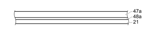
- a dark color film 48a that forms a first dark color layer 48 is provided on the base material 21, and a metal film that forms a conductive layer 47 on the dark color film 48a. 47a is provided.
- the metal film 47a and the dark color film 48a are formed by known methods, for example, a method of attaching a metal foil such as a copper foil, a plating method including electroplating and no electroplating, a sputtering method, a CVD method, a PVD method, and ion plating. It can be formed by a method or a combination of two or more of these.
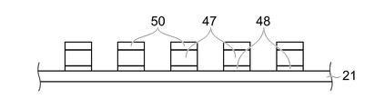
- a resist pattern 50 is provided on the metal film 47a.
- the resist pattern 50 has a shape corresponding to the conductive portion 31 to be formed.
- the resist pattern 50 is provided with the same pattern as the conductive portion 31 to be formed.
- the resist pattern 50 can be formed by patterning using a known photolithography technique.
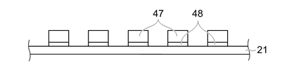
- the metal film 47a and the dark color film 48a are etched using the resist pattern 50 as a mask. By this etching, the metal film 47a and the dark color film 48a are patterned into substantially the same pattern as the resist pattern 50. As a result, as shown in FIG. 9, a conductive layer 47 forming a part of the conductive portion 31 is formed from the patterned metal film 47a. From the patterned dark color film 48a, a first dark color layer 48 that forms a part of the conductive portion 31 is formed.
- the etching method is not particularly limited, and a known method can be adopted. Known methods include, for example, wet etching using an etching solution, plasma etching, and the like. Then, as shown in FIG. 10, the resist pattern 50 is removed.
- the second dark color layer 49 is formed on the surface and the side surface of the conductive layer 47 opposite to the surface on which the first dark color layer 48 is provided.
- the second dark color layer 49 for example, a part of the material forming the conductive layer 47 is subjected to a darkening treatment to form a second dark color layer 49 made of a metal oxide or a metal sulfide from the part of the conductive layer 47. can.
- the darkening process is also called a blackening process.
- a second dark color layer 49 may be provided on the surface of the conductive layer 47.
- the surface of the conductive layer 47 may be roughened to provide the second dark color layer 49.
- the conductor 30 is formed on the base material 21, and the sheet 20 with the conductor is produced.
- the pair of bus bars 25 may be integrally formed with the conductive portion 31 by patterning the metal film 47a, or may be provided separately from the conductive portion 31 provided on the base material 21.
- the manufactured sheet 20 with a conductor is curved according to the shape of the cover 10 to be manufactured. Specifically, first, as shown in FIG. 12, the sheet 20 with a conductor is brought into contact with a mold 60 having a desired shape to be curved. In that state, by applying appropriate heat and pressure to the sheet 20 with a conductor, the sheet 20 with a conductor can be shaped into the shape of the mold 60.
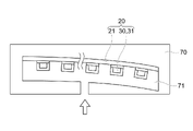
- the cover main body 11 is formed, for example, by injection molding a resin forming the cover main body 11 onto a sheet 20 with a conductor curved into a desired shape. Specifically, first, as shown in FIG. 13, the sheet 20 with a conductor is arranged in the cavity 71 of the mold 70 that matches the shape to be formed. At this time, the sheet 20 with the conductor is arranged so that the side where the conductor 30 is provided is inside the cavity 71 with respect to the base material 21 of the sheet 20 with the conductor. Next, a transparent resin such as acrylic, which has become fluid due to heating, is injected into the cavity 71 of the mold 70.
- a transparent resin such as acrylic, which has become fluid due to heating
- This resin is cooled in the mold 70 and solidified on the sheet 20 with a conductor, so that the cover main body 11 joined to the base material 21 of the sheet 20 with a conductor on the side where the conductor 30 is provided. Is obtained.
- the cover main body portion 11 and the base material 21 of the sheet 20 with a conductor come into contact with each other via a portion between the adjacent conductive portions 31. That is, the conductor 30 is embedded in the cover main body 11. In this way, the cover 10 is manufactured.
- the cover main body 11 may be manufactured separately from the sheet 20 with a conductor.
- the bonding layer 13 is provided on the side of the sheet 20 with a conductor on which the conductor 30 is provided.
- the bonding layer 13 and the base material 21 of the sheet 20 with a conductor come into contact with each other via a portion between the adjacent conductive portions 31. That is, the conductive portion 31 is in a state of being embedded in the bonding layer 13.
- the cover main body 11 and the conductor-attached sheet 20 are joined via the joining layer 13.
- the cover 10 can also be manufactured by such a method.
- the bonding layer 13 a layer made of a material having various adhesiveness or adhesiveness can be used. It is preferable to use a bonding layer 13 having a high visible light transmittance.
- a typical material of such a bonding layer 13 may be, for example, an optical transparent adhesive sheet (OCA: Optical Clear Adhesive) or an optical adhesive (OCR: Optical Clear Resin).
- OCA optical Clear Adhesive
- OCR optical Clear Resin
- the thickness of the bonding layer 13 may be, for example, 0.15 mm or more and 1 mm or less.
- the radio waves will be blocked by the ice or water droplets, and the radio wave device will not be able to properly transmit and / or receive radio waves.
- the plurality of conductive portions 31 located in the first area A1 facing the radio wave device 5 are arranged at the first interval D1.
- the conductor 30 having the conductive portion 31 generates heat when a voltage is applied. The generated heat is transferred to the surface of the cover 10, so that the cover 10 can generate heat. Ice and water droplets adhering to the cover 10 can be removed.
- the first interval D1 is 900 nm or more and 100 mm or less.
- a typical radio wave transmitted and / or received by a radio wave device 5 used for a radar or the like is transmitted between a plurality of conductive portions 31 located in the first area A1. can. Radio waves can be transmitted through the cover 10.
- the plurality of conductive portions 31 located in the first area A1 extend in the same direction. Since the plurality of conductive portions 31 located in the first area A1 extend in the same direction, radio waves are more easily transmitted between the plurality of conductive portions 31 located in the first area A1. Radio waves are less likely to be blocked by the cover 10.
- the direction in which the plurality of conductive portions 31 located in the first area A1 extend is at an angle of 45 ° or more with respect to the plane of polarization 5a of the radio wave. In this case, the area where the plane of polarization 5a of the radio wave comes into contact with the conductive portion 31 can be reduced. The radio waves are less likely to be obstructed by the plurality of conductive portions 31 located in the first area A1.
- the width of the conductive portion 31 is 50 ⁇ m or less. In this case, the transmittance of the light from the light source 3 that passes through the cover 10 can be increased.
- the plurality of conductive portions 31 located in the second area A2 are arranged at the second interval D2.
- the second area A2 faces the light source 3.
- a light source such as an LED that does not easily generate heat is used. Due to the heat generated by the light source 3, it is difficult to remove ice and water droplets adhering to the surface of the cover 10 arranged facing the light source 3. Since a part of the conductor 30 is arranged in the second area A2 facing the light source 3, the second area A2 can generate heat. In the second area A2, ice and water droplets adhering to the surface of the cover 10 can be removed, and the outside can be illuminated by the light from the light source 3.
- the conductive portion 31 Since the light from the light source 3 is strongly emitted along the optical axis, if the conductive portion 31 is arranged on the optical axis, the light transmitted through the cover 10 is significantly reduced due to being hindered by the conductive portion 31. It ends up.
- the plurality of conductive portions 31 located in the second area A2 are arranged at positions away from the intersection of the optical axis of the light source 3 and the cover main body portion 11. The cover 10 makes it easy to transmit the light from the light source 3.
- the second interval D2 is smaller than the first interval D1.
- the calorific value per unit area in the second area A2 is larger than the calorific value per unit area in the first area A1.
- ice and water droplets can be quickly removed from the first area A1 facing the radio wave device 5. That is, the illumination by the light source 3 can be made available in a short time from the radio wave device 5. For example, when it is desired to preferentially use the lighting by the light source 3 over the radio wave device 5, such as when driving a car at night, such a configuration is particularly effective.
- the visible light transmittance of the cover 10 is 50% or more.
- the cover 10 can sufficiently transmit the light from the light source 3.
- the conductive portion 31 has a first dark color layer 48 provided on the opposite side of the conductive layer 47 from the light source 3. With such a first dark color layer 48, it is possible to prevent deterioration of the design of the cover 10 when observed from the outside.
- the cover 10 of the present embodiment is a cover arranged so as to face the radio wave device 5 for transmitting and / or receiving radio waves and the light source 3, and the cover main body portion 11 and the cover main body portion.
- a conductor 30 provided in 11 is provided, the cover main body 11 has light transmission and radio wave transmission, and the cover main body 11 has a first area A1 facing the radio wave device 5 and a light source 3.
- the conductor 30 generates heat when a voltage is applied, and the conductor 30 includes a plurality of conductive portions 31 arranged at intervals, and includes a second zone A2 facing the first zone.
- the plurality of conductive portions 31 located at A1 are arranged at the first interval D1.
- Such a cover 10 can transmit radio waves even if it has a conductor 30.
- the cover 10 is formed in a curved surface shape, but the present invention is not limited to this example, and the cover 10 may be formed in a flat plate shape.
- the cover 10 may be used as a cover for lighting other than the headlight of the automobile 1, for example, as a cover for a tail lamp. It may be used as a cover for lighting provided in railway vehicles, aircraft, ships, spacecraft, etc. other than automobiles. Alternatively, it may be used as a cover for a member other than lighting such as a sensor or an emblem.
- the cover 10 can be used, for example, as a cover for street lights and lighting of buildings, in addition to moving objects. Alternatively, it may be used as a cover for a sensor, a display, or the like provided inside or outdoors of a building.
- the cover 10 is arranged facing both the light source 3 and the radio wave device 5.
- the cover 10 may be arranged so as to face only one of the light source 3 and the radio wave device 5.
- FIG. 15 is a view corresponding to FIG. 4, and is a cross-sectional view showing a modified example of the cover 10.
- the cover 10 is curved so that the side of the base material 21 of the sheet 20 with a conductor is on the outside.
- the cover 10 may be curved so that the side of the base material 21 of the sheet 20 with a conductor is on the inside.
- the sheet 20 with a conductor When the sheet 20 with a conductor is curved so that the side of the base material 21 is inside, the sheet 20 with a conductor is provided so as to form the inner surface of the cover 10. According to such a sheet 20 with a conductor, fogging due to water droplets or the like adhering to the inner surface of the cover 10 can be efficiently removed.
- the sheet 20 with the conductor When the sheet 20 with the conductor is curved so that the side of the base material 21 is on the inside, the sheet 20 with the conductor is shaped into a desired curved shape as compared with the case where the sheet 20 with the conductor is curved so as to be on the outside. When this is done, stress is less likely to be applied to the conductive portion 31, and the conductive portion 31 is less likely to break.
- FIG. 16 is a view corresponding to FIG. 5, and is a plan view showing a modification of the conductor 30.
- the second interval D2 is larger than the first interval D1.
- the calorific value per unit area in the second area A2 is smaller than the calorific value per unit area in the first area A1.
- ice and water droplets can be quickly removed from the second area A2 facing the light source 3.
- the radio wave device 5 can be used in a short time.
- the second area A2 facing the light source 3 also generates heat. In the second area A2, it is possible to make it difficult for water droplets that may hinder the transmission of light to adhere. That is, the anti-fog function can be achieved in the second area A2.
- the arrangement of the conductor 30 is not limited to the examples shown in FIGS. 5 and 16, and the second interval D2 and the first interval D1 may be the same. In this case, the first area A1 and the second area A2 can be uniformly heated.
- FIG. 17 is a view corresponding to FIG. 5, and is a plan view showing another modification of the conductor 30.
- the conductive portion 31 has only the first portion 31a and does not have the second portion 31b.
- the conductor 30 is located only in the first zone A1 and not in the second zone A2.
- radio waves can be transmitted by removing ice and water droplets as in the above-described embodiment. Since the conductor 30 is not arranged in the second area A2, the light from the light source 3 arranged facing the second area A2 is not diffracted by the conductor 30. When observing the light from the light source 3 from the outside, it is difficult to observe the light diffracted by the conductor 30. The visibility is not easily impaired by the diffracted light.
Landscapes
- Engineering & Computer Science (AREA)
- General Engineering & Computer Science (AREA)
- Arrangement Of Elements, Cooling, Sealing, Or The Like Of Lighting Devices (AREA)
Abstract
カバー10は、電波を送信及び/又は受信する電波装置5と光源3とに対面して配置される。カバー10は、カバー本体部11と、カバー本体部11に設けられた導電体30と、を備える。カバー本体部11は、光透過性及び電波透過性を有する。カバー本体部11は、電波装置5に対面する第1区域A1と、光源3に対面する第2区域A2と、を含む。導電体30は、電圧を加えられることによって発熱する。導電体30は、間隔を空けて配列されている複数の導電部31を含む。第1区域A1に位置する複数の導電部31は、第1間隔D1で配列されている。
Description
本発明は、カバーに関する。
自動車等の移動体には、ヘッドライトやテールランプといった外部に光をもたらす照明が設けられている。このような照明は、光源と、カバーと、を有している。
氷や水滴がカバーに付着すると、光源からの光が氷や水滴に遮られることがある。その結果、照明の光が外部に十分にもたらされなくなることがある。カバーに付着した氷や水滴を除去するために、例えば特表2015-506533号公報に記載されているような、導電体を有するカバーが提案されている。
自動車等の移動体に、外部の障害物を検出するための電波装置が搭載されることがある。電波装置は、ミリ波等の電波を外部に発信し、外部で反射した電波を受信する。電波装置は、発信した電波と受信した電波との違いから外部の障害物の位置や大きさ等を検出することができる。しかし、このような電波装置を光源とともにカバーで覆う場合、導電体を有するカバーに電波が遮られて、電波装置が機能しなくなり得るという課題を発見した。
本発明の第1のカバーは、電波を送信及び/又は受信する電波装置と光源とに対面して配置されるカバーであって、
カバー本体部と、
前記カバー本体部に設けられた導電体と、を備え、
前記カバー本体部は、光透過性及び電波透過性を有し、
前記カバー本体部は、前記電波装置に対面する第1区域と、前記光源に対面する第2区域と、を含み、
前記導電体は、電圧を加えられることによって発熱し、
前記導電体は、間隔を空けて配列されている複数の導電部を含み、
前記第1区域に位置する複数の前記導電部は、第1間隔で配列されている。
カバー本体部と、
前記カバー本体部に設けられた導電体と、を備え、
前記カバー本体部は、光透過性及び電波透過性を有し、
前記カバー本体部は、前記電波装置に対面する第1区域と、前記光源に対面する第2区域と、を含み、
前記導電体は、電圧を加えられることによって発熱し、
前記導電体は、間隔を空けて配列されている複数の導電部を含み、
前記第1区域に位置する複数の前記導電部は、第1間隔で配列されている。
本発明の第1のカバーにおいて、前記第1間隔は、900nm以上100mm以下であってもよい。
本発明の第1のカバーにおいて、前記第1区域に位置する複数の前記導電部は、同一の方向に延びていてもよい。
本発明の第1のカバーにおいて、前記第1区域に位置する複数の前記導電部が延びている方向は、前記電波の偏波面に対して45°以上の角度をなしてもよい。
本発明の第1のカバーにおいて、前記導電部の幅は、50μm以下であってもよい。
本発明の第1のカバーにおいて、
前記第2区域に位置する複数の前記導電部は、第2間隔で配列されていてもよい。
前記第2区域に位置する複数の前記導電部は、第2間隔で配列されていてもよい。
本発明の第1のカバーにおいて、前記第2区域は、前記光源の光軸と前記カバー本体部との交点から離れて位置していてもよい。
本発明の第1のカバーにおいて、前記第2間隔は、前記第1間隔より小さくてもよい。
本発明の第1のカバーにおいて、前記第2間隔は、前記第1間隔より大きくてもよい。
本発明の第1のカバーにおいて、前記光源は、LED光源であってもよい。
本発明の第1のカバーにおいて、当該カバーの可視光透過率は、50%以上であってもよい。
本発明の第1のカバーにおいて、前記導電部は、導電層と、前記導電層の前記光源とは逆側に設けられた暗色層と、を有してもよい。
本発明の第2のカバーは、光源に対面して配置されるカバーであって、
カバー本体部と、
前記カバー本体部に設けられた導電体と、を備え、
前記カバー本体部は、光透過性及び電波透過性を有し、
前記カバー本体部は、第1区域と、前記光源に対面する第2区域と、を含み、
前記導電体は、電圧を加えられることによって発熱し、
前記導電体は、間隔を空けて配列されている複数の導電部を有し、
前記第1区域に位置する複数の前記導電部は、第1間隔で配列されている。
カバー本体部と、
前記カバー本体部に設けられた導電体と、を備え、
前記カバー本体部は、光透過性及び電波透過性を有し、
前記カバー本体部は、第1区域と、前記光源に対面する第2区域と、を含み、
前記導電体は、電圧を加えられることによって発熱し、
前記導電体は、間隔を空けて配列されている複数の導電部を有し、
前記第1区域に位置する複数の前記導電部は、第1間隔で配列されている。
本発明の第3のカバーは、電波を送信及び/又は受信する電波装置に対面して配置されるカバーであって、
カバー本体部と、
前記カバー本体部に設けられた導電体と、を備え、
前記カバー本体部は、光透過性及び電波透過性を有し、
前記カバー本体部は、前記電波装置に対面する第1区域と、第2区域と、を含み、
前記導電体は、電圧を加えられることによって発熱し、
前記導電体は、間隔を空けて配列されている複数の導電部を有し、
前記第1区域に位置する複数の前記導電部は、第1間隔で配列されている。
カバー本体部と、
前記カバー本体部に設けられた導電体と、を備え、
前記カバー本体部は、光透過性及び電波透過性を有し、
前記カバー本体部は、前記電波装置に対面する第1区域と、第2区域と、を含み、
前記導電体は、電圧を加えられることによって発熱し、
前記導電体は、間隔を空けて配列されている複数の導電部を有し、
前記第1区域に位置する複数の前記導電部は、第1間隔で配列されている。
本発明の第4のカバーは、電波を送信及び/又は受信する電波装置と光源とに対面して配置されるカバーであって、
本体部と、
前記本体部に設けられた導電体と、を備え、
前記本体部は、光透過性及び電波透過性を有し、
前記導電体は、電圧を加えられることによって発熱し、
前記導電体は、間隔を空けて配列されている複数の導電部を含み、
前記導電体は、前記電波装置に対面する第1部分を含み、
前記第1部分における複数の導電部は、第1間隔で配列されている、
本体部と、
前記本体部に設けられた導電体と、を備え、
前記本体部は、光透過性及び電波透過性を有し、
前記導電体は、電圧を加えられることによって発熱し、
前記導電体は、間隔を空けて配列されている複数の導電部を含み、
前記導電体は、前記電波装置に対面する第1部分を含み、
前記第1部分における複数の導電部は、第1間隔で配列されている、
本発明によれば、導電体を有するカバーに電波を透過させることができる。
以下、図面を参照しながら本発明の一実施の形態について説明する。本件明細書に添付された図面における縮尺及び縦横の寸法比等は、図示と理解のため、実物のそれらから変更し誇張されている。
本明細書において、「板」、「シート」、「フィルム」の用語は、呼称の違いのみに基づいて、互いから区別されるものではない。例えば、「導電体付きシート」は板やフィルムと呼ばれ得るような部材をも含む概念である。例えば、「導電体付きシート」は、「導電体付板」や「導電体付きフィルム」と呼ばれる部材と、呼称の違いのみにおいて区別され得ない。
「シート面」とは、対象となるシート状の部材を全体的かつ大局的に見た場合において対象となるシート状部材の平面方向と一致する面のことを指す。「シート」を「板」または「フィルム」と置き換えた場合も同様である。
本明細書において用いられる、形状や幾何学的条件ならびにそれらの程度を特定する、例えば、「平行」、「直交」、「同一」等の用語ならびに長さや角度の値等は、厳密な意味に縛られることなく、同様の機能を期待し得る程度の範囲を含めて解釈される。
図1乃至図15は、本発明による一実施の形態を説明するための図である。図1は、カバーを備えた自動車を概略的に示す斜視図である。図2は、カバー及びカバーが対面して配置されている光源及び電波装置を示す断面図である。
図1に示されているように、移動体の一例としての自動車1は、照明2を備えている。図1に示されている例では、照明2は、自動車1のヘッドライトである。照明2は、図2に示されているように、光源3と、電波装置5と、カバー10と、を有している。カバー10は、照明2の表面を形成する。カバー10によって区画された空間に、光源3及び電波装置5が配置されている。カバー10は、電波装置5と光源3とに対面して配置されており、電波装置5と光源3とを外部から保護する。光源3は、白色等の所定の色を発光することができる。光源3からの光は、カバー10を透過することで、照明2の外部にもたらされる。光源3からの光がカバー10を十分に透過できるよう、カバー10の可視光透過率は、50%以上であることが好ましく、70%以上であることがより好ましい。光源3は、例えば発光効率が高く長寿命なLED光源であることが好ましい。電波装置5は、電波を送信及び/又は受信する装置である。電波装置5が送信及び/又は受信する電波は、例えば周波数が30~300GHz、30~1200THz、または20kHz~1GHzであってもよい。電波装置5は、例えば、衝突予防システムのレーダに適用されてもよい。図1に示されているように、自動車はバッテリー等の電源7を有している。
カバー10が光源3に対面しているとは、図2に示されているような光源3からの光L1がカバー10に入射することを意味する。カバー10が電波装置5に対面しているとは、図2に示されているような電波装置5からの電波L2がカバー10に入射することを意味する。
図3は、カバー10を概略的に示す斜視図である。図3に示されているように、カバー10は、湾曲した板状の部材である。図4は、図3のIV-IV線に沿ったカバーの断面図である。図4に示されているように、カバー10は、導電体付きシート20の後述する基材21の側が外側となるように湾曲している。図3及び図4に示されているように、カバー10は、カバー本体部11と、カバー本体部11に設けられた導電体付きシート20と、を有している。図2に示された例では、導電体付きシート20は、カバー10の外側表面をなすように設けられている。
カバー本体部11は、導電体付きシート20を支持する。カバー本体部11は、カバー10の形状に合わせた形状に湾曲している。カバー本体部11は、光源3からの光を透過できるよう、透明となっている。カバー本体部11は、光源3からの光を適切に透過可能であれば、無色透明に限らず、顔料等の着色材を含むことで着色透明となっていてもよい。カバー本体部11は、電波装置5が送信及び/又は受信する電波を透過させる。カバー本体部11は、光透過性及び電波透過性を有している。カバー本体部11は、例えばポリエチレンテレフタレート、ポリエチレンナフタレート、ポリカーボネート、ポリスチレン、環状ポリオレフィン等の樹脂や、薄膜状のガラスからなってもよい。カバー本体部11は、1mm以上5mm以下の厚みを有していることが好ましい。このような厚みであると、カバー本体部11に優れた強度及び光学特性を付与できる。
本明細書において、「透明」や「光透過性」とは、当該部材を介して当該部材の一方の側から他方の側を透視し得る程度の透明性を有していることを意味しており、例えば、30%以上、より好ましくは70%以上の可視光透過率を有していることを意味する。「着色透明」とは、特定の波長域の光の透過率が意図的に低くなっているが、可視光全体としての透過率は高くなっており透明になっていることをいう。可視光透過率は、分光光度計((株)島津製作所製「UV-3100PC」、JIS K 0115準拠品)を用いて測定波長380nm~780nmの範囲内で測定したときの、各波長における透過率の平均値として特定される。
本明細書において、「電波透過性」とは、電波装置5が送信及び/又は受信する電波を、電波装置5が適切に機能し得る程度に透過できることを意味しており、例えば、周波数が30~300GHz、30~1200THz、または20kHz~1GHzの電波を80%以上透過できることを意味する。電波の透過率は、ミリ波・マイクロ波透過減衰量測定システム(KEYCOM社製「Model No.RTS01 LAF-26.5A(26.5-110GHz用)」)を用いて測定できる。
カバー本体部11は、第1区域A1と、第2区域A2と、を含んでいる。第1区域A1は、電波装置5に対面する。第2区域A2は、光源3に対面する。第1区域A1は、カバー本体部11のうち、電波装置5からの電波が入射する区域である。第2区域A2は、カバー本体部11のうち、光源3からの光が入射する区域である。第2区域A2は、第1区域A1とは異なる。電波装置5からの電波が入射する区域と光源3からの光が入射する区域とが重なっている場合、当該区域は第1区域A1としてもよい。第2区域A2は、電波装置5からの電波が入射する区域以外の区域としてもよい。第1区域A1及び第2区域A2の大きさや配置は、照明2における光源3及び電波装置5の配置によって適宜に設計される。
導電体付きシート20は、カバー10のシート面に沿ってカバー10と略同一の平面寸法を有して、カバー10の全体にわたって配置されている。導電体付きシート20は、基材21と、導電体30と、一対のバスバー25と、を有している。導電体30は、基材21の一方の面上に設けられている。一対のバスバー25は、導電体30に電気的に接続しており、電圧を加えられることで導電体30に通電させることができる。導電体付きシート20の基材21に対して導電体30が設けられている側が、カバー本体部11が設けられている側となっている。
図3によく示されているように、カバー10は、導電体30に通電するための配線部15を有している。図示された例では、バッテリー等の電源7によって、配線部15から導電体付きシート20のバスバー25を介して導電体30に通電する。導電体30は、電圧を加えられることによって発熱する。導電体30で発生した熱は、カバー10の表面に伝わる。カバー10の表面に伝わった熱により、カバー10の表面に付着した氷や水滴を取り除ける。氷や水滴を除去することで、光源3からの光をカバー10の外部にもたらすことができる。カバー10は電波を透過させるので、電波装置5は正常に機能する。
以下、導電体付きシート20の各構成要素について説明する。
基材21は、バスバー25及び導電体30を支持する部材である。基材21は、透明な電気絶縁性のフィルムである。基材21としては、透明であり、導電体30を適切に支持し得るものであればいかなる材料でもよい。基材21の材料は、例えば、ポリエチレンテレフタレート、ポリエチレンナフタレート、ポリカーボネート、ポリスチレン、環状ポリオレフィン等であってもよい。基材21の厚みは、光透過性や、導電体30の適切な支持性、耐衝撃性、耐久性及び熱伝導性等を考慮すると、30μm以上500μm以下であることが好ましい。カバー本体部11との界面において光の屈折を抑制するために、基材21の屈折率とカバー本体部11の屈折率との差が小さくなっていることが好ましく、同一となっていることがより好ましい。例えば、基材21とカバー本体部11とが同一の材料からなっていてもよい。
一対のバスバー25は、互いに離して配置され、それぞれが対応する配線部15と電気的に接続されている。一対のバスバー25間には、配線部15と接続された電源7の電圧が加えられるようになる。図3等に示された例では、バスバー25は、導電体付きシート20における外縁部近傍に配置されている。一対のバスバー25は、導電体付きシート20の外縁部付近であれば、図3等に示されているように導電体30に対して同じ側に配置されていてもよいし、対向する側に配置されていてもよい。図示されている例に限らず、バスバー25は、基材21に支持されていない位置に設けられていてもよい。例えば、バスバー25は、移動体の外部から観察されない位置、例えば自動車1のボンネットやバンパーに重なる位置に設けられていてもよい。
図5は、導電体付きシート20をそのシート面の法線方向から観察した平面図である。図5においては、理解を容易にするため、湾曲している導電体付きシート20を平板状に示している。
導電体30は、一対のバスバー25間を連結するように配置されており、一対のバスバー25を電気的に接続している。導電体30は、配線部15及びバスバー25を介して電圧を加えられることによって、発熱する。この熱がカバー10の表面に伝わることで、カバー10の表面を発熱させる。
導電体30は、間隔を空けて配列されている複数の導電部31を有している。導電部31は、線状に延びている。複数の導電部31の各々は、一対のバスバー25を連結している。図示された例では、複数の導電部31は、それぞれ独立して一対のバスバー25を連結している。導電部31が均一に発熱するよう、言い換えると導電部31のそれぞれにおける単位長さあたりの発熱量が略同一となるよう、複数の導電部31の抵抗は、略同一となっていることが好ましい。例えば、導電部31の長さが長いほど線幅が小さくなっており、導電部31の長さが短いほど線幅が大きくなっていることで、複数の導電部31の抵抗は、略同一になる。
複数の導電部31は、第1区域A1に位置する第1部分31aと、第2区域A2に位置する第2部分31bと、を含んでいる。第1部分31aとは、第1区域A1に位置する複数の導電部31を意味する。第2部分31bとは、第2区域A2に位置する複数の導電部31を意味する。第1部分31aは、第1間隔D1で配列されている。第2部分31bは、第2間隔D2で配列されている。図5に示されている例では、第1部分31aは、一部の第2部分31bと接続している。第1部分31aは、第2部分31bと接続することで、一対のバスバー25を連結している。第1部分31aと接続していない第2部分31bは、それぞれ一対のバスバー25を連結している。図示されている例に限らず、第1部分31aは、第2部分31bと接続することなく、一対のバスバー25を連結してもよい。
第1間隔D1は、電波装置5が送信及び/又は受信する電波の波長によって適宜設定される。典型的には、第1間隔D1は、900nm以上100mm以下である。例えば当該電波の周波数が30~300GHzのようなミリ波である場合、第1間隔D1は、1mm以上10mm以下であることが好ましい。例えば当該電波の周波数が30~1200THzである場合、第1間隔D1は、250nm以上10μm以下であることが好ましい。例えば当該電波の周波数が20kHz~1GHzのような超音波である場合、第1間隔D1は、0.34μm以上17mm以下であることが好ましい。図5に示された例では、第1間隔D1は、それぞれ同一となっている。第1間隔D1は、それぞれ異なっていてもよい。第1間隔D1は、規則的に変化していてもよいし、不規則に変化していてもよい。第1部分31aは、同一の方向に延びていることが好ましい。図5に示された例では、第1部分31aは、平行に延びている。
図6に示されているように、第1部分31aが延びている方向は、電波装置5が送信及び/又は受信する電波の偏波面5aに対して十分に傾斜していることが好ましい。具体的には、第1部分31aが延びている方向は、電波の偏波面5aに対して45°以上の角度をなしていることが好ましく、60°以上の角度をなしていることが好ましく、90°となっていることが最も好ましい。
偏波面とは、電波が空間を伝搬する際の電場の振動する面のことである。
第2部分31bは、光源3の光軸とカバー本体部11との交点には配置されていないことが好ましい。言い換えると、第2部分31bは、光源3の光軸とカバー本体部11との交点から離れて位置していることが好ましい。
図5に示されている例では、第2間隔D2は、第1間隔D1より小さくなっている。第2区域A2では、第1区域A1より単位面積あたりの発熱量が多くなる。
このようなバスバー25および導電体30の導電部31を構成するための材料は、例えば、金、銀、銅、白金、アルミニウム、クロム、モリブデン、ニッケル、チタン、パラジウム、インジウム、タングステン等の金属、または、これらの金属の1種以上を含んでなる合金の一以上であってもよい。導電体30及びバスバー25は、同一の材料を用いて形成されていてもよいし、或いは、互いに異なる材料を用いて形成されていてもよい。
導電体30は、上述したように不透明な金属材料を用いて形成され得る。図4に示された例では、導電部31は、全体として矩形状の断面を有している。導電部31の幅W、すなわち、カバー10の板面に沿った幅Wは、例えば2μm以上150μm以下であってもよい。特に、後述する導電体30を有する導電体付きシート20の製造工程において導電体付きシート20を湾曲させる際に導電部31が導電体付きシート20に合わせて適切に湾曲するよう、導電部31の幅Wは、150μm以下であることが好ましい。光の透過率が高くなるよう、導電部31の幅Wは、50μm以下であることがより好ましい。カバー10の外観において導電部31が視認されてにくくするために、導電部31の幅Wは、25μm以下であることがさらに好ましい。導電部31の高さH、すなわち、カバー10の板面への法線方向に沿った高さHは、例えば2μm以上15μm以下であってもよい。導電体30によって覆われていない基材21上の面積の割合、すなわち非被覆率は、80%以上99%以下程度と高くなっている。このような導電体30によれば、導電体30が設けられている部分は全体として透明となり、導電体30の存在が光源3からの光や電波装置5が送信及び/又は受信する電波の妨げになりにくい。
図4に示されたように、導電部31は、導電層47、導電層47の表面のうち、基材21に対向する側の面を覆う第1暗色層48と、導電層47の表面のうち、カバー本体部11に覆われる第2暗色層49と、を含むようにしてもよい。本実施の形態において、第1暗色層48は、光源3とは逆側に設けられている。導電部31は、第1暗色層48を含んでいることが好ましい。第2暗色層49が光源3とは逆側に設けられていてもよい。優れた導電性を有する金属材料からなる導電層47は、比較的高い反射率を呈する。導電部31をなす導電層47によって光が反射されると、その反射した光により導電層47が観察されるようになる。外部から導電層47が観察されると、意匠性が低下する場合がある。そこで、第1暗色層48及び第2暗色層49が、導電層47の表面の少なくとも一部分を覆っている。第1暗色層48及び第2暗色層49は、導電層47よりも可視光の反射率が低い層であればよく、例えば黒色等の暗色の層であってもよい。この第1暗色層48及び第2暗色層49によって、導電層47が観察されづらくなる。特に、暗色層48,49が導電層47の光源3とは逆側に設けられていることで、導電層47が観察されづらくなる。外部から観察したときのカバー10の意匠性の低下を防ぐことができる。
図示は省略するが、バスバー25も、金属材料からなる導電層と、導電層の表面に形成された暗色層と、を有していてもよい。暗色層によって比較的高い反射率を呈する導電層が観察されづらくなる。外部から見たときの意匠性の低下を防ぐことができる。
次に、導電体30を有する導電体付きシート20及びカバー10の製造方法について、図7乃至図14を参照しながら説明する。
まず、図7に示されているように、基材21上に第1暗色層48を形成するようになる暗色膜48aを設け、暗色膜48a上に導電層47を形成するようになる金属膜47aを設ける。金属膜47a及び暗色膜48aは、公知の方法、例えば、銅箔等の金属箔を貼着する方法、電界めっき及び無電界めっきを含むめっき法、スパッタリング法、CVD法、PVD法、イオンプレーティング法、又はこれらの二以上を組み合わせた方法で形成され得る。
その後、図8に示されているように、金属膜47a上に、レジストパターン50を設ける。レジストパターン50は、形成されるべき導電部31に対応した形状となっている。図示された例では、レジストパターン50は、形成されるべき導電部31と同一のパターンで設けられている。このレジストパターン50は、公知のフォトリソグラフィー技術を用いたパターニングにより形成できる。
次に、レジストパターン50をマスクとして、金属膜47a及び暗色膜48aをエッチングする。このエッチングにより、金属膜47a及び暗色膜48aがレジストパターン50と略同一のパターンにパターニングされる。この結果、図9に示されているように、パターニングされた金属膜47aから、導電部31の一部をなすようになる導電層47が形成される。パターニングされた暗色膜48aから、導電部31の一部をなすようになる第1暗色層48が形成される。
エッチング方法は特に限られることはなく、公知の方法が採用できる。公知の方法としては、例えば、エッチング液を用いるウェットエッチングや、プラズマエッチングなどが挙げられる。その後、図10に示されているように、レジストパターン50を除去する。
その後、図11に示されているように、導電層47の第1暗色層48が設けられた面と反対側の面及び側面に第2暗色層49を形成する。第2暗色層49は、例えば導電層47をなす材料の一部分に暗色化処理を施して、導電層47をなしていた一部分から、金属酸化物や金属硫化物からなる第2暗色層49を形成できる。暗色化処理は、黒化処理とも呼ばれる。導電層47の表面に第2暗色層49を設けるようにしてもよい。導電層47の表面を粗化して第2暗色層49を設けるようにしてもよい。
以上の工程によって、基材21上に導電体30が形成され、導電体付きシート20が作製される。一対のバスバー25は、金属膜47aのパターニングによって導電部31と一体的に形成されてもよいし、或いは、基材21上に設けられた導電部31とは別途に設けられてもよい。
作製された導電体付きシート20を、製造するカバー10の形状に合わせて湾曲させる。具体的には、まず、図12に示されているように、導電体付きシート20を湾曲させる所望の形状に沿った型60に当接させる。その状態で、導電体付きシート20に適切な熱及び圧力を加えることで、導電体付きシート20を型60の形状に賦形できる。
カバー本体部11は、例えば所望の形状に湾曲された導電体付きシート20にカバー本体部11をなす樹脂を射出成型することで、形成される。具体的には、まず、図13に示されているように、形成される形状に合わせた型70のキャビティ71に導電体付きシート20を配置する。このとき、導電体付きシート20の基材21に対して導電体30が設けられた側がキャビティ71の内側となるように、導電体付きシート20を配置する。次に、型70のキャビティ71の内部に、加熱により流動性を有するようになったアクリル等の透明な樹脂が、射出される。この樹脂が、型70内で冷却され、導電体付きシート20上で固化することで、導電体付きシート20の基材21に対して導電体30が設けられた側に接合したカバー本体部11が得られる。カバー本体部11と導電体付きシート20の基材21とは、隣り合う導電部31の間となる部分を介して接触する。すなわち、導電体30は、カバー本体部11に埋め込まれた状態となる。このようにして、カバー10が製造される。
あるいは、カバー本体部11は、導電体付きシート20とは別途に作製されてもよい。この場合、まず、図14に示されているように、導電体付きシート20の導電体30が設けられた側に接合層13が設けられる。接合層13と導電体付きシート20の基材21とは、隣り合う導電部31の間となる部分を介して接触する。すなわち、導電部31は、接合層13内に埋め込まれた状態となる。接合層13を介して、カバー本体部11と導電体付きシート20とが接合される。このような方法でも、カバー10を製造できる。
接合層13としては、種々の接着性または粘着性を有した材料からなる層を用いることができる。接合層13は、可視光透過率が高いものを用いることが好ましい。このような接合層13の典型的な材料は、例えば、光学用透明粘着シート(OCA:Optical Clear Adhesive)や光学接着剤(OCR:Optical Clear Resin)であってもよい。接合層13の厚みは、例えば0.15mm以上1mm以下であってもよい。
電波装置に対面して配置されるカバーに氷や水滴が付着すると、電波が氷や水滴に遮られて、電波装置が電波を適切に発信及び/又は受信することができない。本実施の形態のカバー10では、電波装置5に対面する第1区域A1に位置する複数の導電部31は、第1間隔D1で配列されている。導電部31を有する導電体30は、電圧を加えられることで発熱する。発生した熱がカバー10の表面に伝わることで、カバー10を発熱させることができる。カバー10に付着した氷や水滴を除去できる。
本実施の形態のカバー10では、第1間隔D1は、900nm以上100mm以下である。第1間隔D1が十分に大きくなっていることで、レーダ等に用いられる電波装置5が送信及び/又は受信する典型的な電波が第1区域A1に位置する複数の導電部31の間を透過できる。カバー10に電波を透過させることができる。
第1区域A1に位置する複数の導電部31は、同一の方向に延びている。第1区域A1に位置する複数の導電部31が同一の方向に延びているため、第1区域A1に位置する複数の導電部31の間を電波がより透過しやすくなっている。カバー10において電波がより遮られにくくなっている。
第1区域A1に位置する複数の導電部31が延びている方向は、電波の偏波面5aに対して45°以上の角度をなしている。この場合、電波の偏波面5aが導電部31と接触する面積を小さくできる。第1区域A1に位置する複数の導電部31により電波が妨げられにくくなる。
導電部31の幅は、50μm以下である。この場合、カバー10を透過する光源3からの光の透過率を高くできる。
第2区域A2に位置する複数の導電部31は、第2間隔D2で配列されている。第2区域A2は、光源3に対面する。光源3としては、LED等の発熱しにくいものが用いられるようになっている。光源3の発熱によって、光源3に対面して配置されるカバー10の表面に付着した氷や水滴を除去することが困難である。光源3に対面する第2区域A2に導電体30の一部が配置されていることで、第2区域A2を発熱させることができる。第2区域A2においてカバー10の表面に付着した氷や水滴を除去することができ、光源3からの光で外部を照明できる。
光源3からの光は光軸に沿って強く放出されるため、光軸上に導電部31が配置されていると、導電部31に妨げられて、カバー10を透過する光が著しく少なくなってしまう。本実施の形態では、第2区域A2に位置する複数の導電部31は、光源3の光軸とカバー本体部11との交点から離れた位置に配置されている。カバー10は、光源3からの光を透過させやすくなっている。
第2間隔D2は、第1間隔D1より小さい。第2区域A2における単位面積あたりの発熱量が、第1区域A1における単位面積あたりの発熱量より多くなる。光源3に対面する第2区域A2において、電波装置5に対面する第1区域A1より氷や水滴を素早く除去することができる。すなわち、電波装置5より光源3による照明を短時間で利用可能にすることができる。例えば夜間に自動車を運転する場合等、電波装置5より光源3による照明を優先的に利用することが望まれる場合、このような構成が特に有効である。
カバー10の可視光透過率は、50%以上である。光源3からの光をカバー10が十分に透過させることができる。
導電部31は、導電層47の光源3とは逆側に設けられた第1暗色層48を有している。このような第1暗色層48により、外部から観察したときのカバー10の意匠性の低下を防ぐことができる。
以上のように、本実施の形態のカバー10は、電波を送信及び/又は受信する電波装置5と光源3とに対面して配置されるカバーであって、カバー本体部11と、カバー本体部11に設けられた導電体30と、を備え、カバー本体部11は、光透過性及び電波透過性を有し、カバー本体部11は、電波装置5に対面する第1区域A1と、光源3に対面する第2区域A2と、を含み、導電体30は、電圧を加えられることによって発熱し、導電体30は、間隔を空けて配列されている複数の導電部31を含み、第1区域A1に位置する複数の導電部31は、第1間隔D1で配列されている。このようなカバー10は、導電体30を有しても電波を透過させることができる。
上述した実施の形態に対して様々な変更を加えることが可能である。
上述した実施の形態において、カバー10が曲面状に形成されている例を示したが、この例に限られず、カバー10が、平板状に形成されていてもよい。
カバー10は、自動車1のヘッドライト以外の照明のカバー、例えばテールランプのカバーとして用いてもよい。自動車以外の、鉄道車両、航空機、船舶、宇宙船等に設けられた照明のカバーとして用いてもよい。あるいは、センサやエンブレム等の照明以外の部材のカバーとして用いられてもよい。
カバー10は、移動体以外にも、例えば街灯や建築物の照明のカバーとして用いることができる。あるいは、建築物の内部や屋外に設けられたセンサや表示物等のカバーとして用いられてもよい。
上述した実施の形態では、カバー10は、光源3と電波装置5との両方に対面して配置されている。カバー10は、光源3と電波装置5とのいずれか一方にのみ対面して配置されていてもよい。
図15は、図4に対応する図であって、カバー10の一変形例を示す断面図である。上述した実施の形態では、カバー10は、導電体付きシート20の基材21の側が外側となるように湾曲している。しかしながら、図15に示されているように、カバー10は、導電体付きシート20の基材21の側が内側となるように湾曲していてもよい。
導電体付きシート20を基材21の側が内側となるように湾曲されている場合、導電体付きシート20は、カバー10の内側表面をなすように設けられる。このような導電体付きシート20によれば、カバー10の内側表面に付着した水滴等による曇りを効率よく除去できる。
導電体付きシート20を基材21の側が内側となるように湾曲させる場合、基材21の側が外側となるように湾曲させる場合に比べて、導電体付きシート20を所望の湾曲形状に賦形する際に導電部31に応力がかかりにくく、導電部31が断線しにくい。
図16は、図5に対応する図であって、導電体30の一変形例を示す平面図である。図16に示された例において、第2間隔D2は、第1間隔D1より大きくなっている。第2区域A2における単位面積あたりの発熱量は、第1区域A1における単位面積あたりの発熱量より少なくなる。電波装置5に対面する第1区域A1において、光源3に対面する第2区域A2より氷や水滴を素早く除去できる。電波装置5を短時間で利用可能にできる。光源3に対面する第2区域A2も発熱する。第2区域A2において、光の透過を妨げ得る水滴を付着しにくくすることができる。すなわち、第2区域A2において、防曇機能を奏することができる。
導電体30の配置は図5や図16に示された例に限らず、第2間隔D2と第1間隔D1とを同一としてもよい。この場合、第1区域A1及び第2区域A2を均一に発熱させることができる。
図17は、図5に対応する図であって、導電体30の他の変形例を示す平面図である。図17に示された例では、導電部31は、第1部分31aのみを有しており、第2部分31bを有していない。言い換えると、導電体30は、第1区域A1にのみ位置しており、第2区域A2には位置していない。第1区域A1においては、上述した実施の形態と同様に、氷や水滴を除去することで、電波を透過させることができる。第2区域A2においては、導電体30が配置されていないため、第2区域A2に対面して配置された光源3からの光が導電体30で回折されてしまうことがない。外部から光源3からの光を観察した際に、導電体30によって回折した光が観察されにくい。回折光によって視界が害されにくい。
1 自動車
2 照明
3 光源
5 電波装置
5a 偏波面
7 電源
10 カバー
11 カバー本体部
13 接合層
15 配線部
20 導電体付きシート
21 基材
25 バスバー
30 導電体
31 導電部
31a 第1部分
31b 第2部分
47 導電層
48 第1暗色層
49 第2暗色層
A1 第1区域
A2 第2区域
D1 第1間隔
D2 第2間隔
2 照明
3 光源
5 電波装置
5a 偏波面
7 電源
10 カバー
11 カバー本体部
13 接合層
15 配線部
20 導電体付きシート
21 基材
25 バスバー
30 導電体
31 導電部
31a 第1部分
31b 第2部分
47 導電層
48 第1暗色層
49 第2暗色層
A1 第1区域
A2 第2区域
D1 第1間隔
D2 第2間隔
Claims (14)
- 電波を送信及び/又は受信する電波装置と光源とに対面して配置されるカバーであって、
カバー本体部と、
前記カバー本体部に設けられた導電体と、を備え、
前記カバー本体部は、光透過性及び電波透過性を有し、
前記カバー本体部は、前記電波装置に対面する第1区域と、前記光源に対面する第2区域と、を含み、
前記導電体は、電圧を加えられることによって発熱し、
前記導電体は、間隔を空けて配列されている複数の導電部を含み、
前記第1区域に位置する複数の前記導電部は、第1間隔で配列されている、カバー。 - 前記第1間隔は、900nm以上100mm以下である、請求項1に記載のカバー。
- 前記第1区域に位置する複数の前記導電部は、同一の方向に延びている、請求項1または2に記載のカバー。
- 前記第1区域に位置する複数の前記導電部が延びている方向は、前記電波の偏波面に対して45°以上の角度をなす、請求項3に記載のカバー。
- 前記導電部の幅は、150μm以下である、請求項1乃至4のいずれか一項に記載のカバー。
- 前記第2区域に位置する複数の前記導電部は、第2間隔で配列されている、請求項1乃至5のいずれか一項に記載のカバー。
- 前記第2区域に位置する複数の前記導電部は、前記光源の光軸と前記カバー本体部との交点から離れて位置している、請求項6に記載のカバー。
- 前記第2間隔は、前記第1間隔より小さい、請求項6または7に記載のカバー。
- 前記第2間隔は、前記第1間隔より大きい、請求項6または7に記載のカバー。
- 前記光源は、LED光源である、請求項1乃至9のいずれか一項に記載のカバー。
- 当該カバーの可視光透過率は、50%以上である、請求項1乃至10のいずれか一項に記載のカバー。
- 前記導電部は、導電層と、前記導電層の前記光源とは逆側に設けられた暗色層と、を含む、請求項1乃至11のいずれか一項に記載のカバー。
- 光源に対面して配置されるカバーであって、
カバー本体部と、
前記カバー本体部に設けられた導電体と、を備え、
前記カバー本体部は、光透過性及び電波透過性を有し、
前記カバー本体部は、第1区域と、前記光源に対面する第2区域と、を含み、
前記導電体は、電圧を加えられることによって発熱し、
前記導電体は、間隔を空けて配列されている複数の導電部を有し、
前記第1区域に位置する複数の前記導電部は、第1間隔で配列されている、カバー。 - 電波を送信及び/又は受信する電波装置に対面して配置されるカバーであって、
カバー本体部と、
前記カバー本体部に設けられた導電体と、を備え、
前記カバー本体部は、光透過性及び電波透過性を有し、
前記カバー本体部は、前記電波装置に対面する第1区域と、第2区域と、を含み、
前記導電体は、電圧を加えられることによって発熱し、
前記導電体は、間隔を空けて配列されている複数の導電部を有し、
前記第1区域に位置する複数の前記導電部は、第1間隔で配列されている、カバー。
Priority Applications (1)
| Application Number | Priority Date | Filing Date | Title |
|---|---|---|---|
| JP2022562201A JPWO2022102743A1 (ja) | 2020-11-13 | 2021-11-12 |
Applications Claiming Priority (2)
| Application Number | Priority Date | Filing Date | Title |
|---|---|---|---|
| JP2020189711 | 2020-11-13 | ||
| JP2020-189711 | 2020-11-13 |
Publications (1)
| Publication Number | Publication Date |
|---|---|
| WO2022102743A1 true WO2022102743A1 (ja) | 2022-05-19 |
Family
ID=81602373
Family Applications (1)
| Application Number | Title | Priority Date | Filing Date |
|---|---|---|---|
| PCT/JP2021/041711 Ceased WO2022102743A1 (ja) | 2020-11-13 | 2021-11-12 | カバー |
Country Status (2)
| Country | Link |
|---|---|
| JP (1) | JPWO2022102743A1 (ja) |
| WO (1) | WO2022102743A1 (ja) |
Cited By (3)
| Publication number | Priority date | Publication date | Assignee | Title |
|---|---|---|---|---|
| WO2025119681A1 (en) * | 2023-12-07 | 2025-06-12 | Valeo Vision | Lighting device and motor vehicle |
| WO2025120112A1 (en) * | 2023-12-07 | 2025-06-12 | Valeo Vision | Lighting device and motor vehicle |
| WO2025201885A1 (en) * | 2024-03-28 | 2025-10-02 | Valeo Vision | Heating film, light-emitting device and motor vehicle |
Citations (2)
| Publication number | Priority date | Publication date | Assignee | Title |
|---|---|---|---|---|
| JP2008052920A (ja) * | 2006-08-22 | 2008-03-06 | Ichikoh Ind Ltd | 車両用灯具および車両用灯具における線ヒータディスペンサー |
| JP2016143914A (ja) * | 2015-01-29 | 2016-08-08 | 大日本印刷株式会社 | 発熱板及び乗り物 |
-
2021
- 2021-11-12 JP JP2022562201A patent/JPWO2022102743A1/ja active Pending
- 2021-11-12 WO PCT/JP2021/041711 patent/WO2022102743A1/ja not_active Ceased
Patent Citations (2)
| Publication number | Priority date | Publication date | Assignee | Title |
|---|---|---|---|---|
| JP2008052920A (ja) * | 2006-08-22 | 2008-03-06 | Ichikoh Ind Ltd | 車両用灯具および車両用灯具における線ヒータディスペンサー |
| JP2016143914A (ja) * | 2015-01-29 | 2016-08-08 | 大日本印刷株式会社 | 発熱板及び乗り物 |
Cited By (3)
| Publication number | Priority date | Publication date | Assignee | Title |
|---|---|---|---|---|
| WO2025119681A1 (en) * | 2023-12-07 | 2025-06-12 | Valeo Vision | Lighting device and motor vehicle |
| WO2025120112A1 (en) * | 2023-12-07 | 2025-06-12 | Valeo Vision | Lighting device and motor vehicle |
| WO2025201885A1 (en) * | 2024-03-28 | 2025-10-02 | Valeo Vision | Heating film, light-emitting device and motor vehicle |
Also Published As
| Publication number | Publication date |
|---|---|
| JPWO2022102743A1 (ja) | 2022-05-19 |
Similar Documents
| Publication | Publication Date | Title |
|---|---|---|
| CN101791966B (zh) | 包括发光纤信号的后视镜组件 | |
| US8783881B2 (en) | Display in the mirror glass and process for production | |
| JP6584072B2 (ja) | 車両用標識灯 | |
| JP2008534351A (ja) | 信号アセンブリ | |
| JP6481386B2 (ja) | 発熱板及び乗り物 | |
| US20050265037A1 (en) | Optics for controlling the direction of light rays and assemblies incorporating the optics | |
| JP2017183063A (ja) | 加熱電極付き合わせガラス板、及び乗り物 | |
| JP7565007B2 (ja) | 導電基板および合わせ板 | |
| JP2016102056A (ja) | 合わせガラス及びその製造方法 | |
| JP6818260B2 (ja) | 発熱板用の中間部材 | |
| JP6589270B2 (ja) | 発熱板用の中間部材 | |
| JP7310370B2 (ja) | 発熱板、導電体付きフィルム及び発熱板の製造方法 | |
| JP6745073B2 (ja) | 導電性パターンシート、発熱板、発熱板を備えた乗り物、及び、発熱板の製造方法 | |
| CN120327433A (zh) | 车辆用外装品和车辆的外装构造 | |
| JP2017112105A (ja) | 発熱板、導電体付きシート、乗り物及び建築物用窓 | |
| JP7405096B2 (ja) | パターン導電体、バスバー付きパターン導電体、合わせ板、仕切部材及び移動体 | |
| JP2019197727A (ja) | 発熱板、導電体付きフィルム及び発熱板の製造方法 | |
| JP2022089004A (ja) | 発熱体、透明発熱カバー | |
| JP2022094697A (ja) | パターン導電体、導電体付きシート、透明発熱カバー及び透明発熱カバーの製造方法 | |
| JP2022092360A (ja) | 導電体付きシート、透明発熱カバー | |
| JP6930583B2 (ja) | 合わせガラスおよび導電性発熱体 | |
| JP6897706B2 (ja) | 発熱板及び乗り物 | |
| JP7800019B2 (ja) | 導電体 | |
| CN221851810U (zh) | 用于车辆的后视镜组件和照明子组件 | |
| JP6631667B2 (ja) | 合わせガラスの製造方法 |
Legal Events
| Date | Code | Title | Description |
|---|---|---|---|
| 121 | Ep: the epo has been informed by wipo that ep was designated in this application |
Ref document number: 21891988 Country of ref document: EP Kind code of ref document: A1 |
|
| ENP | Entry into the national phase |
Ref document number: 2022562201 Country of ref document: JP Kind code of ref document: A |
|
| NENP | Non-entry into the national phase |
Ref country code: DE |
|
| 122 | Ep: pct application non-entry in european phase |
Ref document number: 21891988 Country of ref document: EP Kind code of ref document: A1 |