WO2022097262A1 - 半導体装置および電力変換装置 - Google Patents
半導体装置および電力変換装置 Download PDFInfo
- Publication number
- WO2022097262A1 WO2022097262A1 PCT/JP2020/041487 JP2020041487W WO2022097262A1 WO 2022097262 A1 WO2022097262 A1 WO 2022097262A1 JP 2020041487 W JP2020041487 W JP 2020041487W WO 2022097262 A1 WO2022097262 A1 WO 2022097262A1
- Authority
- WO
- WIPO (PCT)
- Prior art keywords
- region
- outer peripheral
- insulating film
- semiconductor device
- layer
- Prior art date
- Legal status (The legal status is an assumption and is not a legal conclusion. Google has not performed a legal analysis and makes no representation as to the accuracy of the status listed.)
- Ceased
Links
Images











Classifications
-
- H—ELECTRICITY
- H10—SEMICONDUCTOR DEVICES; ELECTRIC SOLID-STATE DEVICES NOT OTHERWISE PROVIDED FOR
- H10D—INORGANIC ELECTRIC SEMICONDUCTOR DEVICES
- H10D30/00—Field-effect transistors [FET]
- H10D30/60—Insulated-gate field-effect transistors [IGFET]
- H10D30/64—Double-diffused metal-oxide semiconductor [DMOS] FETs
- H10D30/66—Vertical DMOS [VDMOS] FETs
- H10D30/665—Vertical DMOS [VDMOS] FETs having edge termination structures
-
- H—ELECTRICITY
- H10—SEMICONDUCTOR DEVICES; ELECTRIC SOLID-STATE DEVICES NOT OTHERWISE PROVIDED FOR
- H10D—INORGANIC ELECTRIC SEMICONDUCTOR DEVICES
- H10D30/00—Field-effect transistors [FET]
- H10D30/01—Manufacture or treatment
- H10D30/021—Manufacture or treatment of FETs having insulated gates [IGFET]
- H10D30/028—Manufacture or treatment of FETs having insulated gates [IGFET] of double-diffused metal oxide semiconductor [DMOS] FETs
- H10D30/0291—Manufacture or treatment of FETs having insulated gates [IGFET] of double-diffused metal oxide semiconductor [DMOS] FETs of vertical DMOS [VDMOS] FETs
-
- H—ELECTRICITY
- H10—SEMICONDUCTOR DEVICES; ELECTRIC SOLID-STATE DEVICES NOT OTHERWISE PROVIDED FOR
- H10D—INORGANIC ELECTRIC SEMICONDUCTOR DEVICES
- H10D62/00—Semiconductor bodies, or regions thereof, of devices having potential barriers
- H10D62/10—Shapes, relative sizes or dispositions of the regions of the semiconductor bodies; Shapes of the semiconductor bodies
- H10D62/102—Constructional design considerations for preventing surface leakage or controlling electric field concentration
- H10D62/103—Constructional design considerations for preventing surface leakage or controlling electric field concentration for increasing or controlling the breakdown voltage of reverse-biased devices
- H10D62/105—Constructional design considerations for preventing surface leakage or controlling electric field concentration for increasing or controlling the breakdown voltage of reverse-biased devices by having particular doping profiles, shapes or arrangements of PN junctions; by having supplementary regions, e.g. junction termination extension [JTE]
-
- H—ELECTRICITY
- H10—SEMICONDUCTOR DEVICES; ELECTRIC SOLID-STATE DEVICES NOT OTHERWISE PROVIDED FOR
- H10D—INORGANIC ELECTRIC SEMICONDUCTOR DEVICES
- H10D62/00—Semiconductor bodies, or regions thereof, of devices having potential barriers
- H10D62/10—Shapes, relative sizes or dispositions of the regions of the semiconductor bodies; Shapes of the semiconductor bodies
- H10D62/102—Constructional design considerations for preventing surface leakage or controlling electric field concentration
- H10D62/103—Constructional design considerations for preventing surface leakage or controlling electric field concentration for increasing or controlling the breakdown voltage of reverse-biased devices
- H10D62/105—Constructional design considerations for preventing surface leakage or controlling electric field concentration for increasing or controlling the breakdown voltage of reverse-biased devices by having particular doping profiles, shapes or arrangements of PN junctions; by having supplementary regions, e.g. junction termination extension [JTE]
- H10D62/106—Constructional design considerations for preventing surface leakage or controlling electric field concentration for increasing or controlling the breakdown voltage of reverse-biased devices by having particular doping profiles, shapes or arrangements of PN junctions; by having supplementary regions, e.g. junction termination extension [JTE] having supplementary regions doped oppositely to or in rectifying contact with regions of the semiconductor bodies, e.g. guard rings with PN or Schottky junctions
-
- H—ELECTRICITY
- H10—SEMICONDUCTOR DEVICES; ELECTRIC SOLID-STATE DEVICES NOT OTHERWISE PROVIDED FOR
- H10D—INORGANIC ELECTRIC SEMICONDUCTOR DEVICES
- H10D62/00—Semiconductor bodies, or regions thereof, of devices having potential barriers
- H10D62/80—Semiconductor bodies, or regions thereof, of devices having potential barriers characterised by the materials
- H10D62/83—Semiconductor bodies, or regions thereof, of devices having potential barriers characterised by the materials being Group IV materials, e.g. B-doped Si or undoped Ge
- H10D62/832—Semiconductor bodies, or regions thereof, of devices having potential barriers characterised by the materials being Group IV materials, e.g. B-doped Si or undoped Ge being Group IV materials comprising two or more elements, e.g. SiGe
- H10D62/8325—Silicon carbide
-
- H—ELECTRICITY
- H10—SEMICONDUCTOR DEVICES; ELECTRIC SOLID-STATE DEVICES NOT OTHERWISE PROVIDED FOR
- H10D—INORGANIC ELECTRIC SEMICONDUCTOR DEVICES
- H10D64/00—Electrodes of devices having potential barriers
- H10D64/111—Field plates
- H10D64/112—Field plates comprising multiple field plate segments
Definitions
- This disclosure relates to a semiconductor device, and more particularly to a semiconductor device having a surface protective film.
- a p-type guard ring region (termination well region) is provided in a so-called termination region in an n-type semiconductor layer, for example, as disclosed in Patent Document 1. It is known.
- the electric field generated when a reverse voltage is applied to the main electrode of the semiconductor device is a depletion layer formed by a pn junction between the n-type semiconductor layer and the p-type guard ring region. It is possible to avoid avalanche breakdown below the rated voltage or breakage at the end of the electrode.
- a p-type impurity region is formed so as to project from the surface electrode and the gate wiring layer to the outer periphery.
- the surface electrode is usually covered with a surface protective film such as polyimide except for a region where wire bonding is performed. Further, the surface electrode may be sealed by using a sealing material such as gel.
- the above-mentioned surface protective film such as polyimide and the encapsulant such as gel tend to contain water in a high humidity environment. Moisture contained in the surface protective film and encapsulant may adversely affect the surface electrodes. Specifically, the surface electrode may dissolve in the water, or a precipitation reaction may occur due to the reaction between the water and the surface electrode.
- the above-mentioned surface protective film such as polyimide and the encapsulant such as gel tend to contain water in a high humidity environment. This moisture can adversely affect the surface electrodes. Specifically, the surface electrode may dissolve in the water, or the water may react with the surface electrode to cause a precipitation reaction. In such a case, the surface electrode and the surface protective film may be cracked, or the surface protective film may be peeled off at the interface between the surface electrode and the surface protective film. If the cracks in the surface electrodes and the surface protective film or the cavities formed by the peeling of the surface protective film act as leak paths, the insulation reliability of the semiconductor device may be impaired.
- the technique according to the present disclosure has been made to solve the above problems, and an object thereof is to provide a semiconductor device having improved insulation reliability.
- the semiconductor device is a semiconductor device having an active region in which a main current flows in the thickness direction of the semiconductor substrate, and the semiconductor substrate has an inner region provided with the active region and an outer region surrounding the inner region.
- the semiconductor device is classified into the first conductive type semiconductor layer and the first conductive type semiconductor layer selectively provided in the upper layer portion of the semiconductor layer so as to surround the inner region in a plan view.
- the termination includes a film, an outer peripheral wiring layer that is at least partially provided above the insulating film and surrounds the inner region in plan view, and an interlayer insulating film that at least covers the insulating film and the outer peripheral wiring layer.
- the well region extends from the boundary between the inner region and the outer region to the outer region, and the surface electrode is provided from the inner region to the upper part of the interlayer insulating film and penetrates the interlayer insulating film.
- the outer peripheral wiring layer is connected to the impurity region via a first contact hole that reaches the impurity region, and the outer peripheral end portion on the outer peripheral side opposite to the inner region in a plan view is described in a plan view. It is provided so as to be located on the inner peripheral side of the outer peripheral end of the terminal well region on the opposite side of the inner region, and further outward from below the end of the surface electrode on the upper part of the interlayer insulating film. Will be.
- the semiconductor device it is possible to suppress the formation of precipitates at the ends of the surface electrodes in the terminal region which is the outer region, and the cracking or peeling of the surface electrodes is suppressed. As a result, it is possible to suppress an increase in leakage current and air discharge due to cracking or peeling of the surface electrode, and it is possible to improve the insulation reliability of the semiconductor device.
- the "active region” of the semiconductor device is defined as the region in which the main current flows when the semiconductor device is on, and the “termination region” of the semiconductor device is defined as the region around the active region. ..
- the "outside” of the semiconductor device means the direction from the central portion to the outer peripheral portion of the semiconductor device, and the “inside” of the semiconductor device means the direction opposite to the "outside”.
- the conductive type of impurities the n-type is defined as the "first conductive type”
- the p-type opposite to the n-type is defined as the “second conductive type”
- the "second conductive type” is defined.
- “1 conductive type” may be defined as p type
- “second conductive type” may be defined as n type.
- MOS Metal-Oxide-Semiconductor
- MOS transistor the field effect transistor having a MOS structure
- the material of the gate insulating film and the gate electrode has been improved from the viewpoint of integration and improvement of the manufacturing process in recent years.
- polycrystalline silicon has been adopted as a material for gate electrodes instead of metal, mainly from the viewpoint of forming source and drain in a self-aligned manner.
- a material having a high dielectric constant is adopted as the material of the gate insulating film, but the material is not necessarily limited to the oxide.
- MOS is not necessarily limited to the metal-oxide-semiconductor laminated structure, and the present specification does not presuppose such limitation. That is, in view of common general technical knowledge, "MOS” here has a meaning not only as an abbreviation derived from the etymology but also broadly including a conductor-insulator-semiconductor laminated structure.
- ordinal numbers such as “first” or “second” may be used in the description described below, these terms facilitate the understanding of the content of the embodiments. It is used for convenience, and is not limited to the order that can be generated by these ordinal numbers.
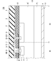
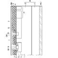
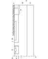
- FIG. 1 is a partial cross-sectional view showing the configuration of the MOSFET 100 which is the semiconductor device according to the first embodiment
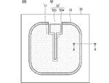
- FIG. 2 is a plan view of the MOSFET 100.
- the cross-sectional view taken along the line AA in FIG. 2 corresponds to FIG. 1.
- the surface protective film 6 (upper surface film) is omitted from the upper surface configuration of the MOSFET 100 for convenience.
- the right side is the termination region of the MOSFET 100
- the left side is the active region in which the main current flows in the ON state of the MOSFET 100.
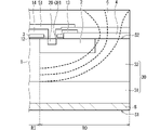
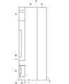
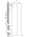
- FIG. 3 is a cross-sectional view showing the configuration of the unit cell UC, which is the smallest unit structure of the MOSFET 100, formed in the inner region RI, which is the active region shown in FIG.
- a plurality of unit cells UC shown in FIG. 3 are arranged in the inner region RI of the MOSFET 100, and the structure shown at the left end of FIG. 1 is the outermost unit cell UC in the inner region RI.
- the MOSFET 100 is formed on an epitaxial substrate 30 composed of a single crystal substrate 31 and an epitaxial layer 32 formed on the upper surface of the single crystal substrate 31.
- the single crystal substrate 31 is a semiconductor substrate composed of n-type (first conductive type) silicon carbide (SiC), and the epitaxial layer 32 is n composed of SiC grown epitaxially on the upper surface of the single crystal substrate 31. It is a type semiconductor layer. That is, the MOSFET 100 is a SiC-PWM.
- the epitaxial substrate 30 is a SiC substrate having a polytype of 4H in the first embodiment.
- a p-type (second conductive type) element well region 9 is selectively formed in the active region, that is, in the upper layer portion of the epitaxial layer 32 in the inner region RI. Further, in the upper layer portion of the element well region 9, an n-type source region 11 and a p-type contact region 19 having a higher impurity concentration than the element well region 9 are selectively formed.
- a p-type terminal well region 2 is selectively formed in the terminal region, that is, in the upper layer portion of the epitaxial layer 32 in the outer region RO surrounding the inner region RI.
- the terminal well region 2 is a frame-shaped (ring-shaped) region surrounding the active region in a plan view, and functions as a so-called guard ring.
- a p-type high concentration region 20 having a relatively high impurity concentration is selectively formed so as to surround the active region.
- the high concentration region 20 is not limited to the p-type, but may be the n-type.
- the n-type region of the epitaxial layer 32 excluding the element well region 9, the source region 11, the contact region 19, and the terminal well region 2 is the drift layer 1 through which a current flows due to drift.
- the impurity concentration of the drift layer 1 is lower than the impurity concentration of the single crystal substrate 31. Therefore, the single crystal substrate 31 has a lower resistivity than the drift layer 1.
- the impurity concentration of the drift layer 1 is, for example, 1 ⁇ 10 14 / cm 3 or more and 1 ⁇ 10 17 / cm 3 or less.
- the terminal well region 2 is formed so as to extend from the boundary between the inner region RI and the outer region RO toward the outer region RO in the upper layer portion of the epitaxial layer 32.
- the inner side (inner peripheral end) of the end well region 2 is defined as the inner region RI, and the outer side thereof is defined as the outer region RO.
- the element well region 9 is sandwiched between the source region 11 and the source region 11 and the drift layer 1.
- the gate insulating film 12 is formed so as to straddle the top and the drift layer 1.
- the gate electrode 3 is formed on the upper surface of the gate insulating film 12.
- the upper layer of the element well region 9 covered with the gate insulating film 12 and the gate electrode 3, that is, the portion of the element well region 9 sandwiched between the source region 11 and the drift layer 1 is formed when the MOSFET 100 is turned on.
- the gate electrode 3 is covered with the interlayer insulating film 14, and the source electrode 51 is formed on the upper surface of the interlayer insulating film 14. Therefore, the gate electrode 3 and the source electrode 51 are electrically insulated by the interlayer insulating film 14.
- the interlayer insulating film 14 has, for example, an elemental composition of boron or phosphorus.
- the gate insulating film 12 and the gate electrode 3 drift on the terminal well region 2 in the outer region RO and on the element well region 9 sandwiched between the source region 11 of the outermost unit cell UC in the inner region RI and the drift layer 1. It is also formed so as to straddle the layer 1, and is led out to the outer region RO, and the gate insulating film 12 and the gate electrode 3 are covered with the interlayer insulating film 14.
- the gate electrode 3 drawn out to the outer region RO is connected to the gate electrode 3 provided in the active region.
- the interlayer insulating film 14 covers the field insulating film 4 so as to extend to the outside of the terminal well region 2.
- a field insulating film 4 having a film thickness thicker than that of the gate insulating film 12 is provided on the upper surface S2 of the epitaxial substrate 30 in the terminal region.
- the field insulating film 4 covers a part of the terminal well region 2 and extends beyond the outer peripheral end of the terminal well region 2 to the outside of the terminal well region 2. Further, the field insulating film 4 is not provided in the inner region RI. In other words, the field insulating film 4 has an opening including the inner region RI in a plan view.
- An outer peripheral wiring layer 13 is formed on the inner edge of the opening of the field insulating film 4 so as to ride on the upper surface of the field insulating film 4 from above the gate insulating film 12, and the gate insulating film 12 or the field insulating film 4 is formed. It is arranged above the terminal well region 2 via.
- the outer peripheral wiring layer 13 is covered with the interlayer insulating film 14 together with the gate insulating film 12.
- a part of the outer peripheral wiring layer 13 is formed so as to extend from the lower side of the edge portion on the outer peripheral side of the source electrode 51 to the outside by 1 ⁇ m or more.
- the source electrode 51 is connected to the source region 11 and the contact region 19 via the contact hole CH 1, and is connected to the high concentration region 20 via the contact hole CH 11.
- the source electrode 51 and the contact region 19 form an ohmic contact via the contact hole CH1. Further, the source electrode 51 and the high concentration region 20 form an ohmic contact or a Schottky contact via the contact hole CH11.
- a back surface electrode 8 that functions as a drain electrode is formed on the lower surface S1 (first main surface) of the epitaxial substrate 30.
- the outer peripheral wiring layer 13 extends to the terminal region outside the outer periphery of the source electrode 51 and substantially surrounds the source electrode 51.
- the source electrode 51 is provided so that a slit portion provided from one side of the source electrode 51, which is substantially rectangular in a plan view, extends to a position of more than half of the source electrode 51, and the gate wiring 52w is inserted therein. .. That is, the gate pad 52p is inserted into the recess provided on one side of the source electrode 51, and the gate portion 52 is provided with the gate wiring 52w inserted into the slit portion continuous with the recess.
- the gate portion 52 is viewed in a plan view. It is formed so as to be surrounded by the source electrode 51 except for a part.
- the source electrode 51 and the gate portion 52 are collectively referred to as a surface electrode 50.
- the gate wiring 52w is electrically connected to the gate electrode 3 drawn out from the active region via a contact hole (not shown), and a gate control signal is given to the gate electrode 3 in the active region.
- the gate portion 52 that is, the gate pad 52p and the gate wiring 52w, functions as an electrode that receives a gate control signal for controlling an electrical path between the source electrode 51 and the back surface electrode 8. As shown in FIG. 2, the gate portion 52 is separated from the source electrode 51 and is electrically insulated from the source electrode 51.
- the surface protective film 6 is formed so as to cover the source electrode 51 and the interlayer insulating film 14 that is not covered by the source electrode 51 and is exposed. However, the surface protective film 6 is the source electrode. An opening is provided in the upper part of the 51 and the upper part of the gate portion 52 (FIG. 2) so that the source electrode 51 and the gate portion 52 can be electrically connected to the outside.
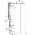
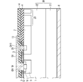
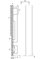
- FIG. 4 is a cross-sectional view showing the configuration of the MOSFET 101 which is a modification of the first embodiment.
- the same components as those of the MOSFET 100 described with reference to FIG. 1 are designated by the same reference numerals, and duplicate description will be omitted.
- the MOSFET 101 has a p-type low-concentration well region 21 provided in the upper layer portion of the drift layer 1 on the outer peripheral side of the terminal well region 2.
- the low-concentration well region 21 is provided as a plurality of frame-shaped regions surrounding the terminal well region 2 in a plan view, but is not limited to the multiplex and may be a single frame-shaped region.
- the impurity concentration in the low concentration well region 21 is equal to or lower than the impurity concentration in the terminal well region 2.
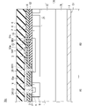
- FIG. 5 is a cross-sectional view showing the configuration of the MOSFET 102, which is a modification of the first embodiment.
- the same components as those of the MOSFET 100 described with reference to FIG. 1 are designated by the same reference numerals, and duplicate description will be omitted.
- the field insulating film 4 is provided so as to extend to the vicinity of the inner edge portion of the terminal well region 2, and the gate electrode 3 drawn out to the outer region RO is provided. It is formed so as to ride on the inner edge portion of the field insulating film 4.
- the source electrode 51 is connected so as to form an ohmic contact or a Schottky contact in the high concentration region 20 via the contact hole CH 12 for the high concentration region 20 through the interlayer insulating film 14 and the field insulating film 4.
- the outer peripheral wiring layer 13 is provided on the field insulating film 4 further outside the contact hole CH 12.
- FIG. 6 is a cross-sectional view showing the configuration of MOSFET 103, which is a modification of the first embodiment.
- the same components as those of the MOSFET 100 described with reference to FIG. 1 are designated by the same reference numerals, and duplicate description will be omitted.
- the field insulating film 4 is provided so as to extend to the vicinity of the inner edge portion of the terminal well region 2, and the gate electrode 3 drawn out to the outer region RO is provided. It is formed so as to ride on the field insulating film 4 and extend to the vicinity of the outer peripheral wiring layer 13.
- the source electrode 51 is connected so as to form an ohmic contact or a Schottky contact in the high concentration region 20 via the contact hole CH 12 for the high concentration region 20 through the interlayer insulating film 14 and the field insulating film 4.
- the outer peripheral wiring layer 13 is provided on the field insulating film 4 further outside the gate electrode 3 extending beyond the contact hole CH 12 and separated from the gate electrode 3.
- FIG. 7 is a plan view showing the configuration of the MOSFET 104, which is a modification of the first embodiment.
- the same components as those of the MOSFET 100 described with reference to FIG. 2 are designated by the same reference numerals, and duplicate description will be omitted.
- the gate portion 52 composed of the gate pad 52p and the gate wiring 52w is provided so as to surround the entire circumference with the source electrode 51 in a plan view, and is provided as an outer peripheral wiring layer. 13 is provided so as to surround the outer periphery of the source electrode 51.
- the precipitation of the insulator at the outer peripheral end of the source electrode 51 can be suppressed in the entire circumference of the terminal region, the cracking and peeling of the source electrode 51 and the surface protective film 6 can be suppressed, and the semiconductor can be suppressed.
- the insulation reliability of the device can be improved.
- FIG. 8 is a cross-sectional view showing the configuration of the MOSFET 105 which is a modification of the first embodiment.
- the same components as those of the MOSFET 100 described with reference to FIG. 1 are designated by the same reference numerals, and duplicate description will be omitted.
- the contact hole CH13 (second contact hole) that penetrates the interlayer insulating film 14 and reaches the outer peripheral wiring layer 13 at the upper part of the outer peripheral wiring layer 13 on the field insulating film 4
- the source electrode 51 and the outer peripheral wiring layer 13 are connected to each other via the contact hole CH13.
- the number of contact holes CH13 is not limited to one, and a plurality of contact holes CH13 may be provided.
- the electric field strength at the outer peripheral end of the source electrode 51 is more effectively relaxed, and by suppressing the precipitation of insulators, cracking and peeling of the source electrode and the upper surface film are suppressed, and the semiconductor is used.
- the insulation reliability of the device can be improved.
- FIG. 9 is a cross-sectional view showing the configuration of the MOSFET 106 which is a modification of the first embodiment.
- the same components as those of the MOSFET 100 described with reference to FIG. 1 are designated by the same reference numerals, and duplicate description will be omitted.
- a contact hole CH13 that penetrates the interlayer insulating film 14 and reaches the outer peripheral wiring layer 13 is provided at the upper part of the outer peripheral wiring layer 13 on the field insulating film 4, and the contact hole CH13 is provided.
- the source electrode 51 and the outer peripheral wiring layer 13 are connected to each other via the structure.
- the contact hole CH 13 is provided at a portion located on the outermost circumference of the source electrode 51, and the outermost circumference of the source electrode 51 and the outer peripheral wiring layer 13 are connected to each other.
- the electric field strength at the outer peripheral end of the source electrode 51 is more effectively relaxed, and by suppressing the precipitation of insulators, cracking and peeling of the source electrode and the upper surface film are suppressed, and the semiconductor is used.
- the insulation reliability of the device can be improved.
- the first state is a state in which a positive voltage equal to or higher than the threshold value is applied to the gate electrode 3, and hereinafter, this state is referred to as an "on state".
- an inverted channel is formed in the channel region.
- the inverting channel is a path for carrier electrons to flow between the source region 11 and the drift layer 1.
- the on state when a high voltage is applied to the back surface electrode 8 with reference to the potential of the source electrode 51, a current flows through the single crystal substrate 31 and the drift layer 1. At this time, the voltage between the source electrode 51 and the back surface electrode 8 is called “on voltage”, and the current flowing between the source electrode 51 and the back surface electrode 8 is called “on current”.
- the on-current flows only in the active region where the channel exists, not in the terminal region.
- the second state is a state in which a voltage less than the threshold value is applied to the gate electrode 3, and hereinafter, this state is referred to as an "off state".
- this state is referred to as an "off state".
- the MOSFET 100 When the MOSFET 100 is in the off state, no inverting channel is formed in the channel region. Therefore, the on-current does not flow. Therefore, when a high voltage is applied between the source electrode 51 and the back surface electrode 8, this high voltage is maintained. At this time, the voltage between the gate electrode 3 and the source electrode 51 is very small with respect to the voltage between the source electrode 51 and the back surface electrode 8, so that also between the gate electrode 3 and the back surface electrode 8. A high voltage will be applied.
- the MOSFET 100 When the MOSFET 100 is in the off state, a high electric field is applied between the drift layer 1 and the element well region 9 and near the interface of the pn junction between the drift layer 1 and the terminal well region 2.
- the voltage to the back surface electrode 8 when this electric field reaches the critical electric field and avalanche breakdown occurs is defined as the maximum voltage (avalanche voltage) of the MOSFET 100.
- the rated voltage is set so that the MOSFET 100 is used in a voltage range in which avalanche breakdown does not occur.
- the depletion layer spreads downward and toward the outer periphery of the drift layer 1, that is, toward the outer region RO from the inner region RI in FIG.
- a depletion layer spreads in the terminal well region 2 from the pn junction interface between the drift layer 1 and the terminal well region 2, and the degree of expansion largely depends on the impurity concentration in the terminal well region 2.
- the impurity concentration in the terminal well region 2 is increased, the spread of the depletion layer in the terminal well region 2 is suppressed, and the tip position of the depletion layer becomes a position close to the boundary between the terminal well region 2 and the drift layer 1. ..
- the position of the tip of the depletion layer can be investigated by TCAD (Technology CAD) simulation or the like.
- TCAD Technology CAD
- a potential difference is generated from the outer peripheral side to the center of the epitaxial layer 32.
- the impurity concentration in the terminal well region 2 is set to the impurity concentration in the lower part of the source electrode 51 and the gate portion 52 so that the upper surface of the terminal well region 2 is not depleted. ..
- the encapsulating resin provided to cover the semiconductor chip may contain moisture.
- the surface protective film 6 (upper surface film) is made of a resin material having high water absorption such as polyimide
- the surface protective film 6 contains a large amount of water under high humidity, and the water content is the epitaxial layer 32 and the epitaxial layer 32. It may reach the top surface of the source electrode 51.
- the surface protective film 6 is made of a material having high moisture resistance such as SiN, cracks are likely to occur in the surface protective film 6 due to stress generated during the process, and the epitaxial layer 32 and the source electrode 51 pass through the cracks. May be exposed to moisture.
- the end portion of the epitaxial layer 32 acts as an anode and the source electrode 51 acts as a cathode in the terminal region due to the voltage applied to the MOSFET 100 in the off state.
- moisture causes an oxygen reduction reaction represented by the following formula (1) and a hydrogen production reaction represented by the formula (2).
- the reaction between aluminum and hydroxide ions is accelerated according to the surrounding electric field strength. Since a potential gradient is generated in the depleted region inside the semiconductor layer, in the MOSFET 100 according to the first embodiment, the potential is located along the upper surface S2 in the region where the depletion layer reaches the upper surface of the epitaxial substrate 30. A gradient occurs.
- FIG. 10 is a diagram illustrating a region where the depletion layer reaches the upper surface of the epitaxial substrate 30, and the equipotential lines are shown by broken lines.
- the region where the potential difference is formed at the boundary between the epitaxial layer 32 and the field insulating film 4 is the region where the depletion layer reaches the upper surface of the epitaxial substrate 30, and is inward due to the impurity concentration in the terminal well region 2. Move closer or closer to the outside.
- the electric resistance generated in the contact region between the source electrode 51 and the terminal well region 2 the sheet resistance of the terminal well region 2 and the pn caused by the high concentration region 20 and the terminal well region 2 generated when the high concentration region 20 is n-type.
- the electric field strength at the lower portion of the source electrode 51 increases.
- the concentration of the terminal well region 2 is low and the depletion layer spreading in the terminal well region 2 from the pn junction interface between the drift layer 1 and the terminal well region 2 reaches the upper surface S2, the depletion layer in the terminal well region 2 is reached.
- a potential gradient is generated along the upper surface S2.
- the region having a high potential on the upper surface S2 approaches the source electrode 51, and the electric field strength at the lower portion of the source electrode 51 further increases.
- the interlayer insulating film 14 When the interlayer insulating film 14 contains boron (B) or phosphorus (P), the interlayer insulating film 14 tends to absorb water as the concentration thereof increases. For example, when the concentration of boron exceeds 2% and the concentration of phosphorus exceeds 5%, the tendency becomes remarkable and the production of aluminum hydroxide is accelerated.
- B boron
- P phosphorus
- the source electrode 51 and the surface protective film 6 are cracked or peeled off due to volume expansion, and a cavity is formed on the upper surface of the interlayer insulating film 14. Moisture entering the cavity may cause an excessive leakage current to flow, or an air discharge may occur in the cavity, which may lead to destruction of the MOSFET 100.
- the outer peripheral end portion of the source electrode 51 is located on the inner peripheral side of the outer peripheral end portion of the terminal well region 2. Therefore, the electric field strength around the source electrode 51 is relaxed.
- the impurity concentration in the terminal well region 2 is set to a certain level or higher, the depletion layer hardly spreads inside the terminal well region 2, and the electric field strength around the gate pad 52p shown in FIG. 2 is effectively relaxed. can do. Therefore, the generation of aluminum hydroxide can be effectively suppressed.
- a region having a high potential on the upper surface S2 is provided by providing the low concentration well region 21 in the upper layer portion of the drift layer 1 on the outer peripheral side of the terminal well region 2 as in the MOSFET 101. Is further away from the source electrode 51, and the electric field strength around the source electrode 51 can be effectively relaxed, and the electric field strength of the epitaxial layer 32 around the outer peripheral end of the end well region 2 can be relaxed. Avalanche voltage can be increased.
- the outer peripheral wiring layer 13 is formed below the outer peripheral end portion of the source electrode 51.
- the outer peripheral wiring layer 13 has a potential between the source electrode 51 and the terminal well region 2, and by moving the potential region away from the source electrode 51 on the outer peripheral side, the source is located around the outer peripheral end of the source electrode 51.
- the electric field concentration due to the potential difference between the electrode 51 and the terminal well region 2 is relaxed.
- the outer peripheral wiring layer 13 is present below the outer peripheral end portion of the source electrode 51 where the electric field is particularly likely to be concentrated, so that the outer peripheral end portion of the lower portion of the source electrode 51 is present.
- the electric field concentration can be relaxed and the generation of aluminum hydroxide can be suppressed.
- the outer peripheral wiring layer 13 extending by 1 ⁇ m or more on the outer peripheral side of the outer peripheral end portion of the source electrode 51, the electric field concentration is effectively alleviated around the outer peripheral end portion of the source electrode 51. , The generation of aluminum hydroxide can be suppressed.
- the electric field concentration is relaxed in all the regions below the outer peripheral end portion of the source electrode 51 to obtain hydroxide.
- the generation of aluminum can be suppressed.
- the source electrode 51 and the outer peripheral wiring layer 13 are connected via the contact hole CH13 which penetrates the interlayer insulating film 14 and reaches the outer peripheral wiring layer 13 at the upper part of the outer peripheral wiring layer 13.
- the potential of the outer peripheral wiring layer 13 can be made the same as the potential of the source electrode 51.
- the potential difference generated between the source electrode 51 and the terminal well region 2 is generated only inside the gate insulating film 12 and the field insulating film 4, and the interlayer insulating film between the source electrode 51 and the outer peripheral wiring layer 13 is generated.
- the potential difference at 14 can be reduced. Therefore, the electric field concentration in the lower part of the outer peripheral end portion of the source electrode 51 can be more effectively relaxed, and the generation of aluminum hydroxide can be suppressed.
- the source electrode 51 and the outer peripheral wiring layer 13 pass through the contact hole CH13 which penetrates the interlayer insulating film 14 and reaches the outer peripheral wiring layer 13 at the outermost peripheral position of the source electrode 51.
- the formation of aluminum hydroxide at the outer peripheral end of the source electrode 51 is suppressed.
- FIGS. 11 to 18 are cross-sectional views showing the manufacturing process in order.
- the description of the method of manufacturing the MOSFET 101 shown in FIG. 4 will be replaced with the description of the method of manufacturing the MOSFET 100.
- a low-resistance single crystal substrate 31 containing n-type impurities at a relatively high concentration (n + ) is prepared.
- the single crystal substrate 31 is a SiC substrate having a polytype of 4H and has an off angle of 4 degrees or 8 degrees.
- FIG. 11 shows by performing epitaxial growth of SiC on the single crystal substrate 31 to form an n-type epitaxial layer 32 having an impurity concentration of 1 ⁇ 10 14 / cm 3 or more and 1 ⁇ 10 17 / cm 3 or less. Obtain the epitaxial substrate 30.
- the step of forming an impurity region in the upper layer of the epitaxial layer 32 is repeated.
- the terminal well region 2, the element well region 9, the contact region 19, the high concentration region 20, the source region 11 and the low concentration well region 21 are formed in the upper layer of the epitaxial layer 32.
- N (nitrogen) or P is used as the n-type impurity
- Al or B is used as the p-type impurity.
- the element well region 9 and the terminal well region 2 can be collectively formed by the same ion implantation process. Further, the contact region 19 and the high concentration region 20 of the terminal well region 2 can be collectively formed by the same ion implantation step.
- the impurity concentration in the element well region 9 is 1.0 ⁇ 10 18 / cm 3 or more and 1.0 ⁇ 10 20 / cm 3 or less.
- the impurity concentration in the source region 11 and the impurity concentration in the contact region 19 are higher than the impurity concentration in the element well region 9, respectively, and are, for example, 1.0 ⁇ 10 19 / cm 3 or more and 1.0 ⁇ 10 21 / cm 3 or less. do.
- the dose amount of the terminal well region 2 is 2.0 ⁇ 10 13 / cm 2 or more in order to secure the amount of impurities that makes it difficult for the depletion layer to spread inside the terminal well region 2 in the off state. It is preferably 5.0 ⁇ 10 13 / cm 2 .
- the dose amount of the low concentration well region 21 is preferably 0.5 ⁇ 10 13 / cm 2 or more and 5 ⁇ 10 13 / cm 2 or less, and is, for example, 1.0 ⁇ 10 13 / cm 2 .
- the implantation energy of ion implantation is, for example, 100 keV or more and 700 keV or less.
- the impurity concentration of the low concentration well region 21 converted from the above dose amount [cm -2 ] is 1 ⁇ 10 17 / cm 3 or more and 1 ⁇ 10 19 / cm 3 or less.
- the impurity is N
- the implantation energy of ion implantation is, for example, 20 keV or more and 300 keV or less.
- an annealing treatment is performed at a temperature of 1500 ° C. or higher using a heat treatment device. This activates the impurities added by ion implantation.
- a SiO 2 film having a thickness of 0.5 ⁇ m or more and 2 ⁇ m or less is formed on the upper surface S2 of the epitaxial substrate 30 by a chemical vapor deposition (CVD) method.
- the field insulating film 4 is formed as shown in FIG. 12 by patterning the SiO 2 film by the photolithography step and the etching step. At this time, the field insulating film 4 is patterned into a shape that covers a part of the terminal well region 2 and extends beyond the end of the terminal well region 2 to the outer peripheral side of the terminal well region 2.
- the SiO 2 film OX1 as the gate insulating film 12 is formed by thermally oxidizing the upper surface of the epitaxial layer 32 not covered with the field insulating film 4. Then, a polycrystalline silicon film PS1 having conductivity is formed on the upper surface of the SiO 2 film OX1 by the reduced pressure CVD method.
- the gate electrode 3 is formed by patterning the polysilicon film PS1 by a photolithography step and an etching step.
- the resist mask in a predetermined layout, the outer peripheral wiring layer 13 can be formed at the same time in the terminal region.
- the SiO 2 film OX2 as the interlayer insulating film 14 is formed by the CVD method.
- the outer peripheral wiring layer 13 is formed so that a part or all of the outer peripheral wiring layer 13 rides on the upper surface of the field insulating film 4, and the outer peripheral end portion of the outer peripheral wiring layer 13 is located on the inner peripheral side of the outer peripheral end portion of the terminal well region 2.
- the outer peripheral wiring layer 13 is not limited to a polycrystalline silicon film, and a metal film having a lower ionization tendency than the source electrode 51 such as Ti (titanium), Ni (nickel), and Au (gold) is subjected to a sputtering method, a vapor deposition method, or the like. It can be formed by patterning and patterning.
- the field insulating film 4 is provided so as to extend to the vicinity of the inner edge portion of the terminal well region 2 and is pulled out to the outer region RO.
- the gate electrode 3 can also be formed so as to ride on the inner edge portion of the field insulating film 4.
- the contact hole CH1 and the high concentration region 20 that penetrate the SiO 2 film OX2 and OX1 and reach the contact region 19 and the source region 11 are reached by the photolithography step and the etching step.
- the contact hole CH11 is formed.
- the SiO 2 film OX1 becomes the gate insulating film 12
- the SiO 2 film OX2 becomes the interlayer insulating film 14.
- the MOSFETs 105 and 106 shown in FIGS. 8 and 9 can be obtained by forming the contact hole CH13 that penetrates the interlayer insulating film 14 and reaches the outer peripheral wiring layer 13 on the outer peripheral side of the contact hole CH11. ..
- the interlayer insulating film 14 can also be formed of a BPSG (boron phosphorus silicate glass) in which B and P are doped in SiO 2 , or a multilayer film containing SiO 2 , SiN, BPSG and the like.
- BPSG boron phosphorus silicate glass
- the shape of the step is smoothed by an annealing treatment at 1000 ° C. As a result, the implantability of the electrode in the contact hole is improved, so that a fine structure can be formed.
- a material that becomes a surface electrode 50 such as a gate portion 52 including a source electrode 51, a gate pad 52p, and a gate wiring 52w on the upper surface S2 of the epitaxial substrate 30 by a sputtering method or a vapor deposition method.
- Form layer ML1 a material that becomes a surface electrode 50 such as a gate portion 52 including a source electrode 51, a gate pad 52p, and a gate wiring 52w on the upper surface S2 of the epitaxial substrate 30 by a sputtering method or a vapor deposition method.
- the material layer ML2 of the back surface electrode 8 is formed on the lower surface S1 of the epitaxial substrate 30 by the same method as the material layer ML1.
- the material layer ML1 for example, a metal containing any one or more of Ti (titanium), Ni (nickel), Al, Cu (copper), Au (gold), or Al such as Al-Si. An alloy or the like is used.
- a metal containing any one or more of Ti, Ni, Al, Cu, and Au is used.
- the portion where the material layer ML1 and the material layer ML2 are in contact with the epitaxial substrate 30 may be formed with a silicide film in advance by heat treatment.
- the back surface electrode 8 can also be formed at the end of all steps.
- the material layer ML1 is patterned by a photolithography step and an etching step to separate the source electrode 51 and the gate portion 52 (including the gate pad 52p and the gate wiring 52w) from the surface electrode.
- Form 50 the material layer ML1 is patterned by a photolithography step and an etching step to separate the source electrode 51 and the gate portion 52 (including the gate pad 52p and the gate wiring 52w) from the surface electrode.
- the source electrode 51 is formed so that the outer peripheral wiring layer 13 is located below the outer peripheral end portion of the source electrode 51.
- the outer peripheral wiring layer 13 can be formed not only in the portion of the line AA in FIG. 2 but also in all the regions below the outer peripheral end portion of the source electrode 51.
- the MOSFET 101 shown in FIG. 4 can be obtained. If the low-concentration well region 21 is not formed in the step described with reference to FIG. 11, the MOSFET 100 shown in FIG. 1 can be obtained.
- the surface protective film 6 is processed into a desired shape by, for example, a polyimide coating step, a photolithography step, and an etching step. Further, the surface protective film 6 can also be formed by depositing a SiN film by a CVD method and performing a photolithography step and an etching step.
- the MOSFET 100 according to the first embodiment, it is possible to suppress the formation of aluminum hydroxide at the end of the source electrode 51 in the terminal region, and the source electrode 51 and the surface protective film can be suppressed. Cracking or peeling of 6 is suppressed. As a result, it is possible to suppress an increase in leakage current and air discharge due to cracking or peeling of the source electrode 51 and the surface protective film 6, and it is possible to improve the insulation reliability of the MOSFET 100.
- FIG. 19 is a plan view showing the configuration of the MOSFET 200 which is the semiconductor device according to the second embodiment. Further, FIG. 20 is a cross-sectional view taken along the line BB in FIG. 19 in the direction of arrow viewing. In FIG. 19, the surface protective film 6 (upper surface film) is omitted from the upper surface configuration of the MOSFET 200 for convenience.
- the gate wiring 52w connected to the gate pad 52p in the terminal region, that is, the outer region RO, is the gate pad 52p in a plan view. Is provided so as to surround the source pad 51p except for the portion where the source pad 51p is formed. Further, the source wiring 51w connected to the source pad 51p is provided so as to surround the gate pad 52p and the gate wiring 52w in a plan view.
- the source electrode 51 is formed by the source pad 51p and the source wiring 51w
- the gate portion 52 is formed by the gate pad 52p and the gate wiring 52w.
- the high-concentration region 20 of the terminal well region 2 is provided so as to extend below the source wiring 51w, and the source wiring 51w is provided with the field insulating film 4 and the interlayer insulating film 14. It is connected so as to form an ohmic contact or a Schottky contact with the high concentration region 20 via a contact hole CH3 that penetrates the terminal well region 2 and reaches the high concentration region 20.
- the field insulating film 4 is provided so as to extend to the vicinity of the inner edge portion of the terminal well region 2, and the gate electrode is drawn out to the outer region RO. 3 is formed so as to ride on the inner edge portion of the field insulating film 4 and further extend to the outer peripheral side, and the gate wiring 52w penetrates the interlayer insulating film 14 and reaches the gate electrode 3 in the contact hole CH2. Is connected to the gate electrode 3 so as to form an ohmic contact or a Schottky contact.
- the gate pad 52p and the gate wiring 52w do not necessarily have to be directly connected, and may be electrically connected via, for example, the gate electrode 3.
- the source pad 51p and the source wiring 51w do not necessarily have to be directly connected, and may be electrically connected via, for example, the outer peripheral wiring layer 13.
- the outer peripheral wiring layer 13 is formed below the outer peripheral end portion of the source wiring 51w. Further, the outer peripheral wiring layer 13 is formed so as to extend from below the outer peripheral end portion of the source wiring 51w to the outside by 1 ⁇ m or more. The outer peripheral wiring layer 13 can be formed in all the regions below the outer peripheral end portion of the source wiring 51w.
- the outer peripheral wiring layer 13 is formed below the inner peripheral end portion of the source wiring 51w. Further, the outer peripheral wiring layer 13 is formed so as to extend further inward by 1 ⁇ m or more from below the inner peripheral end portion of the source wiring 51w. The outer peripheral wiring layer 13 can be formed in all the regions below the inner peripheral end portion of the source wiring 51w.
- FIG. 21 is a cross-sectional view showing the configuration of MOSFET 201, which is a modification of the second embodiment.
- the same components as those of the MOSFET 200 described with reference to FIG. 20 are designated by the same reference numerals, and duplicate description will be omitted.
- the MOSFET 201 has a p-type low-concentration well region 21 provided in the upper layer portion of the drift layer 1 on the outer peripheral side of the terminal well region 2.
- the low-concentration well region 21 is provided as a plurality of frame-shaped regions surrounding the terminal well region 2 in a plan view, but is not limited to the multiplex and may be a single frame-shaped region.
- the impurity concentration in the low concentration well region 21 is equal to or lower than the impurity concentration in the terminal well region 2.
- the outer peripheral wiring layer 13 penetrates the interlayer insulating film 14 at the upper part of the outer peripheral wiring layer 13 on the field insulating film 4.
- the contact hole CH13 to reach is provided, and the source wiring 51w and the outer peripheral wiring layer 13 may be connected to each other via the contact hole CH13.
- the number of contact holes CH13 is not limited to one, and a plurality of contact holes CH13 may be provided.
- the electric field strength of the source wiring 51w is more effectively relaxed, and by suppressing the precipitation of insulators, cracking and peeling of the source wiring 51w and the surface protective film 6 are suppressed, and the semiconductor device is used. Insulation reliability can be improved.
- a contact hole CH 13 which penetrates the interlayer insulating film 14 and reaches the outer peripheral wiring layer 13 is provided at the upper part of the outer peripheral wiring layer 13.
- the outermost circumference of the source wiring 51w and the outer peripheral wiring layer 13 may be connected to each other via the contact hole CH13.
- the electric field strength at the outermost periphery of the source wiring 51w is more effectively relaxed, and by suppressing the precipitation of insulators, cracking and peeling of the source wiring 51w and the surface protective film 6 are suppressed. , The insulation reliability of the semiconductor device can be improved.
- FIG. 22 is a cross-sectional view showing the configuration of the MOSFET 202, which is a modification of the second embodiment.
- the same components as those of the MOSFET 200 described with reference to FIG. 20 are designated by the same reference numerals, and duplicate description will be omitted.
- a contact hole CH4 (third contact hole) that penetrates the interlayer insulating film 14 and reaches the outer peripheral wiring layer 13 is provided at the position of the inner peripheral end portion of the source wiring 51w.
- the source wiring 51w and the outer peripheral wiring layer 13 are connected to each other at the innermost circumference of the source wiring 51w.
- the electric field strength at the inner peripheral end of the source wiring 51w is more effectively relaxed, and by suppressing the precipitation of insulators, cracking and peeling of the source electrode and the upper surface film are suppressed.
- the insulation reliability of the semiconductor device can be improved.
- the MOSFET 200 according to the second embodiment also has an “on state” in which a positive voltage equal to or higher than the threshold value is applied to the gate electrode 3 and a threshold value on the gate electrode 3. It operates separately from the “off state” in which a voltage less than less than is applied.
- the impurity concentration in the terminal well region 2 is usually set to the impurity concentration in the lower part of the source electrode 51 and the gate portion 52 so that the inside of the terminal well region 2 is not depleted.
- the encapsulating resin provided to cover the semiconductor chip may contain moisture.
- the surface protective film 6 (upper surface film) is made of a resin material having high water absorption such as polyimide
- the surface protective film 6 contains a large amount of water under high humidity, and the water content is the epitaxial layer 32 and the epitaxial layer 32. It may reach the top surface of the source electrode 51.
- the surface protective film 6 is made of a material having high moisture resistance such as SiN, cracks are likely to occur in the surface protective film 6 due to stress generated during the process, and the epitaxial layer 32 and the source electrode 51 pass through the cracks. May be exposed to moisture.
- the end portion of the epitaxial layer 32 acts as an anode and the source electrode 51 acts as a cathode in the terminal region due to the voltage applied to the MOSFET 200 in the off state.
- the concentration of hydroxide ions increases as described in the first embodiment. This hydroxide ion chemically reacts with the source electrode 51.
- the source electrode 51 is made of aluminum, the aluminum may be aluminum hydroxide.
- the source wiring 51w is closer to the end of the epitaxial layer 32 which is the anode than the source pad 51p, and aluminum hydroxide is likely to be generated in the source wiring 51w.
- the reaction between aluminum and hydroxide ions is accelerated according to the surrounding electric field strength. Since a potential gradient is generated in the depleted region inside the semiconductor layer, in the MOSFET 200, a potential gradient along the upper surface S2 is generated in the region where the depletion layer reaches the upper surface of the epitaxial substrate 30. Since this potential gradient is also formed in the field insulating film 4 and the interlayer insulating film 14 formed on the upper surface S2 of the epitaxial layer 32, an electric field is generated around the outer peripheral end of the source wiring 51w. As a result, when the electric field strength at the outer peripheral end of the source wiring 51w exceeds a certain level, an aluminum hydroxide formation reaction occurs, and the reaction is accelerated as the electric field strength increases.
- an electric field is generated around the inner peripheral end portion of the source wiring 51w due to the potential difference between the source wiring 51w and the terminal well region 2 and the potential difference between the source wiring 51w and the gate wiring 52w.
- the source wiring 51w and the surface protective film 6 are cracked or peeled due to volume expansion, and a cavity is formed on the upper surface of the interlayer insulating film 14. Moisture entering the cavity may cause an excessive leakage current to flow, or air discharge may occur in the cavity, which may lead to destruction of the MOSFET 200.
- the outer peripheral end portion of the source wiring 51w is located on the inner peripheral side of the outer peripheral end portion of the terminal well region 2. Therefore, the electric field strength around the source wiring 51w is relaxed.
- the impurity concentration in the terminal well region 2 is set to a certain level or higher, the depletion layer hardly spreads inside the terminal well region 2, and the electric field strength around the source wiring 51w can be effectively relaxed. .. Therefore, the generation of aluminum hydroxide can be effectively suppressed.
- the electric field strength around the source wiring 51w is effectively relaxed, and the terminal well region 2 is provided.
- the electric field strength of the epitaxial layer 32 can be relaxed around the outer peripheral end portion of the MOSFET 200, and the avalanche voltage of the MOSFET 200 can be increased.
- the outer peripheral wiring layer 13 is formed below the outer peripheral end portion of the source wiring 51w, and the inner peripheral wiring layer 13 is formed in the source wiring 51w.
- the outer peripheral wiring layer 13 is formed below the peripheral end portion.
- the outer peripheral wiring layer 13 has a potential between the source wiring 51w and the terminal well region 2, and the potential region is moved away from the outer peripheral end portion of the source wiring 51w to the outer peripheral side and the inner peripheral end portion to the inner peripheral side.
- the electric potential concentration due to the potential difference between the source wiring 51w and the terminal well region 2 is relaxed around the outer peripheral end portion and the inner peripheral end portion of the source wiring 51w.
- the outer peripheral wiring layer 13 is present below the outer peripheral end portion and the inner peripheral end portion of the source wiring 51w where the electric field is particularly easy to concentrate, so that the outer peripheral portion of the source wiring 51w is present.
- the electric field concentration at the lower part of the end portion and the lower part of the inner peripheral end portion can be relaxed to suppress the generation of aluminum hydroxide.
- the outer peripheral wiring layer 13 is formed so as to extend 1 ⁇ m or more on the outer peripheral side of the outer peripheral end portion of the source wiring 51w and 1 ⁇ m or more on the inner peripheral side of the inner peripheral end portion, whereby the source electrode 51 is formed.
- the electric field concentration is effectively alleviated around the outer peripheral end portion and the inner peripheral end portion, and the generation of aluminum hydroxide can be suppressed.
- the outer peripheral wiring layer 13 penetrates the interlayer insulating film 14 at the upper part of the outer peripheral wiring layer 13 on the field insulating film 4.
- the potential of the outer peripheral wiring layer 13 can be made the same as the potential of the source electrode 51.
- the potential difference generated between the source wiring 51w and the terminal well region 2 is generated only inside the gate insulating film 12 and the field insulating film 4, and the interlayer insulating film between the source wiring 51w and the outer peripheral wiring layer 13 is generated.
- the potential difference at 14 can be reduced. Therefore, the electric field concentration at the outer peripheral end of the lower portion of the source wiring 51w can be more effectively alleviated, and the generation of aluminum hydroxide can be suppressed.
- the source electrode 51 and the outer peripheral wiring layer 13 pass through the contact hole CH13 that penetrates the interlayer insulating film 14 and reaches the outer peripheral wiring layer 13 at the outermost peripheral position of the source wiring 51w.
- the formation of aluminum hydroxide at the outer peripheral end of the source electrode 51 is suppressed.
- the contact hole CH13 which penetrates the interlayer insulating film 14 and reaches the outer peripheral wiring layer 13 at the upper part of the outer peripheral wiring layer 13 is used.
- the outermost circumference of the source wiring 51w and the outer peripheral wiring layer 13 may be connected to each other.
- the interlayer insulating film 14 is penetrated into the outer peripheral wiring layer 13 at the position of the inner peripheral end portion of the source wiring 51w. It is also possible to match the configuration in which the innermost circumference of the source wiring 51w and the outer peripheral wiring layer 13 are connected via the contact hole CH4 that reaches.
- the source wiring 51w and the outer peripheral wiring layer 13 are connected to each other via the contact hole at the outermost circumference and the innermost circumference of the source wiring 51w, so that the outer peripheral end portion and the inner peripheral end portion of the lower portion of the source wiring 51w are connected. It is possible to sufficiently suppress the electric field concentration of the part and suppress the generation of aluminum hydroxide.
- the formation of aluminum hydroxide at the end of the source wiring 51w is suppressed.
- FIGS. 23 to 31 are sectional views showing the manufacturing process in order.
- the description of the method of manufacturing the MOSFET 201 shown in FIG. 21 will be replaced with the description of the method of manufacturing the MOSFET 200.
- the same steps as the manufacturing method of the MOSFET 100 of the first embodiment described with reference to FIGS. 1 to 18 will be omitted as appropriate.
- a low-resistance single crystal substrate 31 containing n-type impurities at a relatively high concentration (n + ) is prepared, and SiC is epitaxially grown on the single crystal substrate 31 to form an epitaxial layer 32 in FIG. 23.
- the epitaxial substrate 30 shown in the above is obtained.
- FIG. 23 As shown in the above, the terminal well region 2, the element well region 9, the contact region 19, the high concentration region 20, the source region 11 and the low concentration well region 21 are formed in the upper layer of the epitaxial layer 32.
- the SiO 2 film is formed on the upper surface S2 of the epitaxial substrate 30 by the CVD method, and the SiO 2 film is patterned by the photolithography step and the etching step to form the field insulating film 4 as shown in FIG. 24. ..
- the field insulating film 4 is patterned into a shape that covers a part of the terminal well region 2 and extends beyond the end of the terminal well region 2 to the outer peripheral side of the terminal well region 2.
- the upper surface of the epitaxial layer 32 not covered with the field insulating film 4 is thermally oxidized to form the SiO 2 film OX1 as the gate insulating film 12, and then the SiO 2 film.
- a conductive polycrystalline silicon film PS1 is formed on the upper surface of the OX1 by a reduced pressure CVD method.
- the gate electrode 3 is formed by patterning the polycrystalline silicon film PS1 by a photolithography step and an etching step.
- the outer peripheral wiring layer 13 is simultaneously formed in the terminal region.
- the outer peripheral wiring layer 13 is provided on the outer peripheral side of the gate electrode 3 formed so as to partially ride on the upper surface of the field insulating film 4, and the outer peripheral end portion is the inner circumference of the outer peripheral end portion of the terminal well region 2. It is formed so as to be located on the side.
- the SiO 2 film OX2 as the interlayer insulating film 14 is formed by the CVD method.
- the contact hole CH1 and the high concentration region 20 that penetrate the SiO 2 film OX2 and OX1 and reach the contact region 19 and the source region 11 are reached by the photolithography step and the etching step.
- the contact hole CH11 is formed.
- the contact hole CH2 penetrating the interlayer insulating film 14 and reaching the gate electrode 3 the contact hole CH3 penetrating the interlayer insulating film 14 and the field insulating film 4 to the high concentration region 20.
- the SiO 2 film OX1 becomes the gate insulating film 12
- the SiO 2 film OX2 becomes the interlayer insulating film 14.
- a material layer ML1 to be a surface electrode 50 such as 52 is formed.
- the material layer ML2 of the back surface electrode 8 is formed on the lower surface S1 of the epitaxial substrate 30 by the same method as that of the material layer ML1.
- the material layer ML1 is patterned by a photolithography step and an etching step to form a source electrode 51 (including a source pad 51p and a source wiring 51w) and a gate portion 52 (gate pad 52p and gate wiring). (Including 52w) is separated to form the surface electrode 50.
- the source wiring 51w is formed so that the outer peripheral wiring layer 13 is located below the outer peripheral end portion and the inner peripheral portion of the source wiring 51w.
- the outer peripheral wiring layer 13 can be formed not only in the portion of the line BB in FIG. 20 but also in all the regions below the outer peripheral end portion and the inner peripheral end portion of the source wiring 51w.
- the precipitation of the insulating material at the outer peripheral end portion and the inner peripheral end portion of the source wiring 51w is suppressed in the entire circumference of the terminal region, and the cracking and peeling of the source wiring 51w and the surface protective film 6 are suppressed. , The insulation reliability of the semiconductor device can be improved.
- the MOSFET 201 shown in FIG. 21 can be obtained. If the low-concentration well region 21 is not formed in the step described with reference to FIG. 23, the MOSFET 200 shown in FIG. 20 can be obtained.
- the MOSFET 200 according to the second embodiment it is possible to suppress the generation of aluminum hydroxide at the end of the source wiring 51w in the terminal region, and the source wiring 51w and the surface protective film can be suppressed. Cracking or peeling of 6 is suppressed. As a result, it is possible to suppress an increase in leakage current and aerial discharge due to cracking or peeling of the source wiring 51w and the surface protective film 6, and it is possible to improve the insulation reliability of the MOSFET 200.
- the MOSFET is exemplified as the semiconductor device of the first and second embodiments, but the present invention is not limited to this, and a transistor other than the MOSFET, for example, a JFET (JunctionFET), an IGBT (InsulatedGate Bipolar Transistor), or the like is used.
- a transistor other than the MOSFET for example, a JFET (JunctionFET), an IGBT (InsulatedGate Bipolar Transistor), or the like is used.
- JFET JointFET
- IGBT InsulatedGate Bipolar Transistor
- MOSFET 100 of the first embodiment and the MOSFET 200 of the second embodiment are exemplified as planar type transistors, the present disclosure can also be applied to trench type transistors.
- the power conversion device and the method for manufacturing the power conversion device according to the third embodiment will be described.
- the third embodiment applies the semiconductor device according to the first and second embodiments described above to the power conversion device, and in the following description, the configurations described in the first and second embodiments. Components similar to the elements are illustrated with the same reference numerals, and detailed description thereof will be omitted as appropriate.
- the applicable power conversion device is not limited to that of a specific application, but the case where it is applied to a three-phase inverter will be described below.
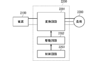
- FIG. 32 is a block diagram schematically showing the configuration of a power conversion system including the power conversion device 2200 according to the third embodiment.
- the power conversion system shown in FIG. 32 has a power supply 2100, a power conversion device 2200, and a load 2300.
- the power supply 2100 is a DC power supply and supplies DC power to the power conversion device 2200.
- the power supply 2100 can be configured with various things, for example, a DC system, a solar cell, a storage battery, or the like. Further, the power supply 2100 can be configured by a rectifier circuit or an AC-DC converter connected to an AC system. Further, the power supply 2100 can also be configured by a DC-DC converter that converts the DC power output from the DC system into a predetermined power.
- the power converter 2200 is a three-phase inverter connected between the power supply 2100 and the load 2300.
- the power conversion device 2200 converts the DC power supplied from the power supply 2100 into AC power, and supplies the AC power to the load 2300.
- the power conversion device 2200 outputs a drive signal for driving each switching element of the conversion circuit 2201 that converts DC power into AC power and outputs the conversion circuit 2201. It includes a drive circuit 2202 and a control circuit 2203 that outputs a control signal for controlling the drive circuit 2202 to the drive circuit 2202.
- the load 2300 is a three-phase electric motor driven by AC power supplied from the power conversion device 2200.
- the load 2300 is not limited to a specific application, and is an electric motor mounted on various electric devices.
- the load 2300 is used as an electric motor for a hybrid vehicle, an electric vehicle, a railway vehicle, an elevator, or an air conditioning device.
- the details of the power conversion device 2200 will be described below.
- the conversion circuit 2201 includes a switching element and a freewheeling diode (not shown). Then, when the switching element performs the switching operation, the DC power supplied from the power supply 2100 is converted into AC power and further supplied to the load 2300.
- the conversion circuit 2201 is a two-level three-phase full bridge circuit, and has six switching elements and their respective switching. It can be composed of six freewheeling diodes connected in antiparallel to the element.
- the semiconductor device according to any one of the above-described embodiments 1 and 2 is applied to each switching element in the conversion circuit 2201.
- the six switching elements are connected in series for each of the two switching elements to form an upper and lower arm, and each upper and lower arm constitutes each phase (U phase, V phase and W phase) of the full bridge circuit. Then, the output terminals of the upper and lower arms, that is, the three output terminals of the conversion circuit 2201 are connected to the load 2300.
- the drive circuit 2202 generates a drive signal for driving the switching element of the conversion circuit 2201, and supplies the drive signal to the control electrode of the switching element of the conversion circuit 2201. Specifically, based on the control signal output from the control circuit 2203 described later, a drive signal for turning on the switching element and a drive signal for turning off the switching element are output to the control electrodes of the respective switching elements. do.
- the drive signal When the switching element is kept on, the drive signal is a voltage signal (on signal) equal to or higher than the threshold voltage of the switching element, and when the switching element is kept off, the drive signal is a voltage lower than the threshold voltage of the switching element. It becomes a signal (off signal).
- the control circuit 2203 controls the switching element of the conversion circuit 2201 so that the desired power is supplied to the load 2300. Specifically, the time (on time) for each switching element of the conversion circuit 2201 to be in the on state is calculated based on the power to be supplied to the load 2300.
- the conversion circuit 2201 can be controlled by pulse width modulation (PWM) control that modulates the on-time of the switching element according to the voltage to be output.
- PWM pulse width modulation
- control circuit 2203 gives a control command to the drive circuit 2202 so that an on signal is output to the switching element that should be turned on at each time point and an off signal is output to the switching element that should be turned off. Control signal) is output.
- the drive circuit 2202 outputs an on signal or an off signal as a drive signal to the control electrodes of the respective switching elements based on the control signal.
- the semiconductor device according to any one of the above-described first and second embodiments is applied as the switching element of the conversion circuit 2201, the on-resistance after the energization cycle is stabilized. be able to.
- the semiconductor device according to the first and second embodiments When the semiconductor device according to the first and second embodiments is applied to the power conversion device 2200 as described above, the semiconductor device is usually used by being embedded in a gel or a resin, but these materials also completely block water. Therefore, the insulation protection of the semiconductor device is maintained by the configuration shown in the first and second embodiments. That is. By applying the semiconductor device having the configuration shown in the first and second embodiments, the reliability of the power conversion device 2200 can be enhanced.
- the semiconductor devices of the first and second embodiments are applied to the two-level three-phase inverter
- the application examples of the semiconductor devices of the first and second embodiments are limited to this.
- the semiconductor devices of the first and second embodiments can be applied to various power conversion devices.
- the two-level power conversion device has been described, but the semiconductor devices of the first and second embodiments can be applied to the three-level or multi-level power conversion device. Further, in the case of supplying electric power to the single-phase load, the semiconductor devices of the first and second embodiments can be applied to the single-phase inverter.
- the semiconductor devices of the first and second embodiments can be applied to the DC-DC converter or the AC-DC converter.
- the power conversion device to which the semiconductor devices of the first and second embodiments are applied is not limited to the case where the load described above is an electric motor, and is not limited to, for example, an electric discharge machine, a laser machine, and an induction heating cooker. It can also be used as a power supply for a device or contactless power supply system. Further, the power conversion device to which the semiconductor devices of the first and second embodiments are applied can also be used as a power conditioner in a solar power generation system, a power storage system, or the like.
- the semiconductor device is manufactured by the manufacturing method described in the first and second embodiments.
- the conversion circuit 2201 having the semiconductor device is incorporated into the power conversion device 2200.
- the conversion circuit 2201 is a circuit for converting and outputting the input power.
- the drive circuit 2202 is incorporated in the power conversion device 2200.
- the drive circuit 2202 is a circuit for outputting a drive signal for driving the semiconductor device to the semiconductor device.
- the control circuit 2203 is incorporated in the power conversion device 2200.
- the control circuit 2203 is a circuit for outputting a control signal for controlling the drive circuit 2202 to the drive circuit 2202.
- the semiconductor switching element has shown an example of being composed of a SiC semiconductor, it can be a switching element composed of a wideband gap semiconductor other than the SiC semiconductor. ..
- Wide bandgap semiconductors that are non-Si semiconductors include gallium nitride-based materials or diamond, in addition to silicon carbide.
- a switching element composed of a wide bandgap semiconductor can be used even in a high voltage region where unipolar operation is difficult with a Si semiconductor, and switching loss generated during switching operation can be greatly reduced. Therefore, it is possible to greatly reduce the power loss.
- switching elements composed of wide bandgap semiconductors have low power loss and high heat resistance. Therefore, when a power module including a cooling unit is configured, the heat radiation fins of the heat sink can be miniaturized, so that the semiconductor module can be further miniaturized.
- the switching element composed of the wide bandgap semiconductor is suitable for high frequency switching operation. Therefore, when applied to a converter circuit in which a high frequency demand is high, the reactor or capacitor connected to the converter circuit can be miniaturized by increasing the switching frequency.
- each component of the present disclosure includes structures having other structures or shapes as long as they perform the same function.
- each embodiment can be freely combined, and each embodiment can be appropriately modified or omitted.
Landscapes
- Electrodes Of Semiconductors (AREA)
Abstract
Description
以下の説明において、半導体装置の「活性領域」とは半導体装置のオン状態において主電流が流れる領域であり、半導体装置の「終端領域」とは、活性領域の周囲における領域であるものと定義する。また、以下において、半導体装置の「外側」とは半導体装置の中央部から外周部に向かう方向を意味し、半導体装置の「内側」とは「外側」に対して反対の方向を意味する。また、以下の記載では、不純物の導電型に関して、n型を「第1導電型」、n型とは反対導電型のp型を「第2導電型」として定義するが、その逆に「第1の導電型」をp型、「第2の導電型」をn型と定義しても良い。
以下、実施の形態1の半導体装置の構成、動作および製造方法について説明する。
図1は、実施の形態1に係る半導体装置であるMOSFET100の構成を示す部分断面図であり、図2は、MOSFET100の平面図である。なお、図2におけるA-A線での矢視方向断面図が図1に対応する。なお、図2においては、便宜的にMOSFET100の上面構成のうち、表面保護膜6(上面膜)を省略している。また、図1において、右側がMOSFET100の終端領域であり、左側がMOSFET100のオン状態において主電流が流れる活性領域である。
図4は、実施の形態1の変形例であるMOSFETの101の構成を示す断面図である。なお、図4においては、図1を用いて説明したMOSFET100と同一の構成については同一の符号を付し、重複する説明は省略する。
図5は、実施の形態1の変形例であるMOSFETの102の構成を示す断面図である。なお、図5においては、図1を用いて説明したMOSFET100と同一の構成については同一の符号を付し、重複する説明は省略する。
図6は、実施の形態1の変形例であるMOSFETの103の構成を示す断面図である。なお、図6においては、図1を用いて説明したMOSFET100と同一の構成については同一の符号を付し、重複する説明は省略する。
図7は、実施の形態1の変形例であるMOSFETの104の構成を示す平面図である。なお、図7においては、図2を用いて説明したMOSFET100と同一の構成については同一の符号を付し、重複する説明は省略する。
図8は、実施の形態1の変形例であるMOSFETの105の構成を示す断面図である。なお、図8においては、図1を用いて説明したMOSFET100と同一の構成については同一の符号を付し、重複する説明は省略する。
図9は、実施の形態1の変形例であるMOSFETの106の構成を示す断面図である。なお、図9においては、図1を用いて説明したMOSFET100と同一の構成については同一の符号を付し、重複する説明は省略する。
次に、図1および図2を用いて説明した実施の形態1のMOSFET100の動作を、2つの状態に分けて説明する。
H2O + e- → OH- + 1/2H2 ・・・(2)
これに伴い、ソース電極51の近傍で水酸化物イオンの濃度が増加する。この水酸化物イオンは、ソース電極51と化学的に反応する。例えば、ソース電極51がアルミニウムで構成される場合は、上記の化学反応によってアルミニウムが水酸化アルミニウムとなることがある。
次に、製造工程を順に示す断面図である図11~図18を用いて、実施の形態1のMOSFET100の製造方法について説明する。なお、以下では、図4に示したMOSFET101の製造方法の説明をもってMOSFET100の製造方法の説明に替える。
以下、実施の形態2の半導体装置の構成、動作および製造方法について説明する。なお、以下の説明においては、実施の形態1のMOSFET100と同一の構成については同一の符号を付し、重複する説明は省略する。
図19は、本実施の形態2に係る半導体装置であるMOSFET200の構成を示す平面図である。また、図20は、図19におけるB-B線での矢視方向断面図である。なお、図19においては、便宜的にMOSFET200の上面構成のうち、表面保護膜6(上面膜)を省略している。
図21は、実施の形態2の変形例であるMOSFETの201の構成を示す断面図である。なお、図21においては、図20を用いて説明したMOSFET200と同一の構成については同一の符号を付し、重複する説明は省略する。
また、図8に示された実施の形態1の変形例であるMOSFETの105のように、フィールド絶縁膜4上の外周配線層13の上部において層間絶縁膜14を貫通して外周配線層13に達するコンタクトホールCH13が設けられ、コンタクトホールCH13を介してソース配線51wと外周配線層13とが接続された構成とすることもできる。なお、コンタクトホールCH13は1つに限らず、複数設けることができる。
次に、図19および図20を用いて説明した実施の形態2のMOSFET200の動作について説明する。
次に、製造工程を順に示す断面図である図23~図31を用いて、実施の形態2のMOSFET200の製造方法について説明する。なお、以下では、図21に示したMOSFET201の製造方法の説明をもってMOSFET200の製造方法の説明に替える。なお、図1~図18を用いて説明した実施の形態1のMOSFET100の製造方法と同一の工程については適宜説明を省略する。
以上説明した実施の形態1および2の半導体装置では、エピタキシャル基板30の材料としてSiCを用いる例を示したが、これに限定されるものではなく、エピタキシャル基板30の材料としては、窒化ガリウム(GaN)など他のワイドバンドギャップ半導体を用いることもできる。
また、実施の形態1のMOSFET100および実施の形態2のMOSFET200は、プレーナ型のトランジスタとして例示したが、トレンチ型のトランジスタに本開示を適用することもできる。
本実施の形態3に係る電力変換装置および電力変換装置の製造方法について説明する。本実施の形態3は、以上に記載された実施の形態1および2に係る半導体装置を電力変換装置に適用するものであり、以下の説明においては、実施の形態1および2で説明された構成要素と同様の構成要素については同じ符号を付して図示し、その詳細な説明については適宜省略するものとする。
適用する電力変換装置は特定の用途のものに限定されるものではないが、以下では、三相のインバータに適用する場合について説明する。
次に、本実施の形態3に関する電力変換装置の製造方法を説明する。まず、実施の形態1および2に記載された製造方法で半導体装置を製造する。そして、当該半導体装置を有する変換回路2201を電力変換装置2200に組み込む。変換回路2201は、入力される電力を変換して出力するための回路である。
Claims (16)
- 半導体基板の厚み方向に主電流が流れる活性領域を有する半導体装置であって、
前記半導体基板は、
前記活性領域が設けられた内側領域と前記内側領域を囲む外側領域とに区分され、
前記半導体装置は、
第1導電型の半導体層と、
平面視において前記内側領域を囲むように前記半導体層の上層部に選択的に設けられた、前記第1導電型とは異なる導電型の第2導電型の終端ウェル領域と、
前記終端ウェル領域の上層部に選択的に設けられた第1または第2導電型の不純物領域と、
前記半導体基板の第1の主面とは反対側の第2の主面側に設けられた表面電極と、
前記第1の主面上に設けられた裏面電極と、
前記終端ウェル領域の上部を部分的に覆うように設けられた絶縁膜と、
少なくとも一部が前記絶縁膜の上部に設けられ、平面視において前記内側領域を囲む外周配線層と、
前記絶縁膜および前記外周配線層を少なくとも覆う層間絶縁膜と、を備え、
前記終端ウェル領域は、
前記内側領域と前記外側領域との境界から前記外側領域に延在し、
前記表面電極は、前記内側領域から前記層間絶縁膜の上部にかけて設けられ、前記層間絶縁膜を貫通して前記不純物領域に達する第1のコンタクトホールを介して前記不純物領域に接続され、
前記外周配線層は、
平面視において前記内側領域とは反対側である外周側の外周端部が、平面視において前記内側領域とは反対側の前記終端ウェル領域の外周端部よりも内周側に位置すると共に、前記層間絶縁膜の上部の前記表面電極の端部の下方から、さらに外側に位置するように設けられる、半導体装置。 - 前記外周配線層は、
前記内側領域を囲む全周において、前記外周端部が、前記層間絶縁膜の上部の前記表面電極の前記端部の下方から、さらに外側に位置するように設けられる、請求項1記載の半導体装置。 - 前記外周配線層は、
前記外周端部が、前記層間絶縁膜の上部の前記表面電極の前記端部の下方から少なくとも1μmさらに外側に位置するように設けられる、請求項1記載の半導体装置。 - 前記表面電極は、
前記層間絶縁膜を貫通して前記外周配線層に達する第2のコンタクトホールを介して前記外周配線層に接続される、請求項1記載の半導体装置。 - 前記表面電極は、
前記層間絶縁膜の上部の前記端部において、前記第2のコンタクトホールを介して前記外周配線層に接続される、請求項4記載の半導体装置。 - 半導体基板の厚み方向に主電流が流れる活性領域を有する半導体装置であって、
前記半導体基板は、
前記活性領域が設けられた内側領域と前記内側領域を囲む外側領域とに区分され、
前記半導体装置は、
第1導電型の半導体層と、
平面視において前記内側領域を囲むように前記半導体層の上層部に選択的に設けられた、前記第1導電型とは異なる導電型の第2導電型の終端ウェル領域と、
前記終端ウェル領域の上層部に選択的に設けられた第1または第2導電型の不純物領域と、
前記半導体基板の第1の主面とは反対側の第2の主面側に設けられた表面電極と、
前記第1の主面上に設けられた裏面電極と、
前記終端ウェル領域の上部を部分的に覆うように設けられた絶縁膜と、
少なくとも一部が前記絶縁膜の上部に設けられた外周配線層と、
前記絶縁膜および前記外周配線層を少なくとも覆う層間絶縁膜と、を備え、
前記終端ウェル領域は、
前記内側領域と前記外側領域との境界から前記外側領域に延在し、
前記内側領域は、
トランジスタの最小単位構造が複数設けられて前記活性領域を構成し、
前記表面電極は、
前記トランジスタのゲート電極に電気的に接続されるゲート部と、
前記トランジスタのソース領域電極に電気的に接続されるソース電極と、を有し、
前記ゲート電極は、
少なくとも一部が前記絶縁膜の上部に設けられ、
前記ソース電極は、
前記内側領域から前記層間絶縁膜の上部にかけて設けられ、前記層間絶縁膜を貫通して前記不純物領域に達する第1のコンタクトホールを介して前記不純物領域に接続されるソースパッドと、前記ソースパッドと接続されるソース配線と、を含み、
前記ゲート部は、
前記ソースパッドから離間して、平面視で前記ソースパッドを囲むように前記層間絶縁膜の上部に設けられ、前記層間絶縁膜を貫通して前記絶縁膜の上部の前記ゲート電極に達する第2のコンタクトホールを介して前記ゲート電極に接続されるゲート配線と、前記ゲート配線に接続されるゲートパッドと、を含み、
前記ソース配線は、前記ゲート配線と離間して、平面視で前記ゲート配線を囲むように前記層間絶縁膜の上部に設けられ、
前記外周配線層は、
平面視において前記ゲート電極を囲むように前記絶縁膜上に設けられ、
前記内側領域とは反対側である外周側の外周端部が、平面視において前記内側領域とは反対側の前記終端ウェル領域の外周端部よりも内周側に位置すると共に、前記ソース配線の外周端部の下方から、さらに外側に位置し、かつ、前記ソース配線の内周端部の下方から、さらに内側に位置するように設けられる、半導体装置。 - 前記外周配線層は、
前記ゲート電極を囲む全周において、前記外周端部が、前記ソース配線の前記外周端部の下方から、さらに外側に位置し、かつ、前記ソース配線の前記内周端部の下方から、さらに内側に位置するように設けられる、請求項6記載の半導体装置。 - 前記外周配線層は、
前記外周端部が、前記ソース配線の前記外周端部の下方から少なくとも1μmさらに外側に位置し、かつ、前記ソース配線の前記内周端部の下方から少なくとも1μmさらに内側に位置するように設けられる、請求項6記載の半導体装置。 - 前記ソース配線は、
前記層間絶縁膜を貫通して前記外周配線層に達する第3のコンタクトホールを介して前記外周配線層に接続される、請求項6記載の半導体装置。 - 前記ソース配線は、
前記ソース配線の前記外周端部において前記第3のコンタクトホールを介して前記外周配線層に接続される、請求項9記載の半導体装置。 - 前記ソース配線は、
前記ソース配線の前記内周端部において前記第3のコンタクトホールを介して前記外周配線層に接続される、請求項9記載の半導体装置。 - 前記半導体層は、炭化珪素半導体層である、請求項1または請求項6記載の半導体装置。
- 前記層間絶縁膜は、ホウ素またはリンの元素組成を有する、請求項1または請求項6記載の半導体装置。
- 前記終端ウェル領域の単位面積当たりの不純物濃度が2×1013cm-2以上である、請求項1または請求項6記載の半導体装置。
- 前記半導体基板は、
前記半導体層の上層部に選択的に設けられた、第2の導電型のウェル領域を有し、
前記ウェル領域は、
前記終端ウェル領域の不純物濃度以下の不純物濃度を有する、請求項1または請求項6記載の半導体装置。 - 請求項1から請求項15のうちの何れか1項に記載の半導体装置を有し、入力される電力を変換して出力する変換回路と、
前記半導体装置を駆動するための駆動信号を前記半導体装置に出力する駆動回路と、
前記駆動回路を制御するための制御信号を前記駆動回路に出力する制御回路と、を備える、電力変換装置。
Priority Applications (5)
| Application Number | Priority Date | Filing Date | Title |
|---|---|---|---|
| PCT/JP2020/041487 WO2022097262A1 (ja) | 2020-11-06 | 2020-11-06 | 半導体装置および電力変換装置 |
| US18/031,365 US12464767B2 (en) | 2020-11-06 | 2020-11-06 | Semiconductor device and power conversion device |
| JP2022560592A JP7459292B2 (ja) | 2020-11-06 | 2020-11-06 | 半導体装置および電力変換装置 |
| CN202080106392.3A CN116368623B (zh) | 2020-11-06 | 2020-11-06 | 半导体装置以及电力变换装置 |
| DE112020007758.6T DE112020007758T5 (de) | 2020-11-06 | 2020-11-06 | Halbleitereinheit und leistungswandlereinheit |
Applications Claiming Priority (1)
| Application Number | Priority Date | Filing Date | Title |
|---|---|---|---|
| PCT/JP2020/041487 WO2022097262A1 (ja) | 2020-11-06 | 2020-11-06 | 半導体装置および電力変換装置 |
Publications (1)
| Publication Number | Publication Date |
|---|---|
| WO2022097262A1 true WO2022097262A1 (ja) | 2022-05-12 |
Family
ID=81457053
Family Applications (1)
| Application Number | Title | Priority Date | Filing Date |
|---|---|---|---|
| PCT/JP2020/041487 Ceased WO2022097262A1 (ja) | 2020-11-06 | 2020-11-06 | 半導体装置および電力変換装置 |
Country Status (5)
| Country | Link |
|---|---|
| US (1) | US12464767B2 (ja) |
| JP (1) | JP7459292B2 (ja) |
| CN (1) | CN116368623B (ja) |
| DE (1) | DE112020007758T5 (ja) |
| WO (1) | WO2022097262A1 (ja) |
Cited By (1)
| Publication number | Priority date | Publication date | Assignee | Title |
|---|---|---|---|---|
| WO2025074874A1 (ja) * | 2023-10-05 | 2025-04-10 | ローム株式会社 | 半導体装置 |
Citations (6)
| Publication number | Priority date | Publication date | Assignee | Title |
|---|---|---|---|---|
| JP2008235331A (ja) * | 2007-03-16 | 2008-10-02 | Nissan Motor Co Ltd | 炭化珪素半導体装置及びその製造方法 |
| WO2010125661A1 (ja) * | 2009-04-30 | 2010-11-04 | 三菱電機株式会社 | 半導体装置及びその製造方法 |
| JP2013026563A (ja) * | 2011-07-25 | 2013-02-04 | Mitsubishi Electric Corp | 炭化珪素半導体装置 |
| WO2015178024A1 (ja) * | 2014-05-23 | 2015-11-26 | パナソニックIpマネジメント株式会社 | 炭化珪素半導体装置 |
| JP2019192678A (ja) * | 2018-04-18 | 2019-10-31 | ルネサスエレクトロニクス株式会社 | 半導体装置 |
| WO2020208761A1 (ja) * | 2019-04-11 | 2020-10-15 | 三菱電機株式会社 | 半導体装置および電力変換装置 |
Family Cites Families (12)
| Publication number | Priority date | Publication date | Assignee | Title |
|---|---|---|---|---|
| JP5026019B2 (ja) * | 2006-08-08 | 2012-09-12 | 三菱電機株式会社 | 薄膜トランジスタ基板、薄膜トランジスタの製造方法、及び表示装置 |
| JP5751763B2 (ja) * | 2010-06-07 | 2015-07-22 | 三菱電機株式会社 | 半導体装置 |
| JP5687128B2 (ja) * | 2011-05-06 | 2015-03-18 | 三菱電機株式会社 | 半導体装置およびその製造方法 |
| JP5640969B2 (ja) | 2011-12-26 | 2014-12-17 | 三菱電機株式会社 | 半導体素子 |
| DE112013005788B4 (de) | 2012-12-04 | 2019-02-07 | Denso Corporation | Halbleitervorrichtung und Verfahren zu deren Fertigung |
| JP6580270B2 (ja) | 2016-08-25 | 2019-09-25 | 三菱電機株式会社 | 炭化珪素半導体装置 |
| WO2018055719A1 (ja) * | 2016-09-23 | 2018-03-29 | 三菱電機株式会社 | 炭化珪素半導体装置 |
| US9985125B1 (en) | 2016-11-25 | 2018-05-29 | Panasonic Intellectual Property Management Co., Ltd. | Silicon carbide semiconductor device |
| CN115274855B (zh) * | 2017-02-24 | 2025-10-28 | 三菱电机株式会社 | 碳化硅半导体装置以及电力变换装置 |
| DE112017007186B4 (de) | 2017-03-07 | 2024-06-27 | Mitsubishi Electric Corporation | Halbleitereinheit und leistungswandler |
| JP7013735B2 (ja) * | 2017-09-05 | 2022-02-01 | 富士電機株式会社 | 炭化珪素半導体装置および炭化珪素半導体装置の製造方法 |
| JP7085959B2 (ja) * | 2018-10-22 | 2022-06-17 | 三菱電機株式会社 | 半導体装置 |
-
2020
- 2020-11-06 US US18/031,365 patent/US12464767B2/en active Active
- 2020-11-06 DE DE112020007758.6T patent/DE112020007758T5/de active Pending
- 2020-11-06 WO PCT/JP2020/041487 patent/WO2022097262A1/ja not_active Ceased
- 2020-11-06 JP JP2022560592A patent/JP7459292B2/ja active Active
- 2020-11-06 CN CN202080106392.3A patent/CN116368623B/zh active Active
Patent Citations (6)
| Publication number | Priority date | Publication date | Assignee | Title |
|---|---|---|---|---|
| JP2008235331A (ja) * | 2007-03-16 | 2008-10-02 | Nissan Motor Co Ltd | 炭化珪素半導体装置及びその製造方法 |
| WO2010125661A1 (ja) * | 2009-04-30 | 2010-11-04 | 三菱電機株式会社 | 半導体装置及びその製造方法 |
| JP2013026563A (ja) * | 2011-07-25 | 2013-02-04 | Mitsubishi Electric Corp | 炭化珪素半導体装置 |
| WO2015178024A1 (ja) * | 2014-05-23 | 2015-11-26 | パナソニックIpマネジメント株式会社 | 炭化珪素半導体装置 |
| JP2019192678A (ja) * | 2018-04-18 | 2019-10-31 | ルネサスエレクトロニクス株式会社 | 半導体装置 |
| WO2020208761A1 (ja) * | 2019-04-11 | 2020-10-15 | 三菱電機株式会社 | 半導体装置および電力変換装置 |
Cited By (1)
| Publication number | Priority date | Publication date | Assignee | Title |
|---|---|---|---|---|
| WO2025074874A1 (ja) * | 2023-10-05 | 2025-04-10 | ローム株式会社 | 半導体装置 |
Also Published As
| Publication number | Publication date |
|---|---|
| US20230378342A1 (en) | 2023-11-23 |
| CN116368623A (zh) | 2023-06-30 |
| US12464767B2 (en) | 2025-11-04 |
| CN116368623B (zh) | 2025-07-29 |
| JP7459292B2 (ja) | 2024-04-01 |
| DE112020007758T5 (de) | 2023-08-17 |
| JPWO2022097262A1 (ja) | 2022-05-12 |
Similar Documents
| Publication | Publication Date | Title |
|---|---|---|
| JP6870119B2 (ja) | 半導体装置および電力変換装置 | |
| JP2021182639A (ja) | 半導体装置および電力変換装置 | |
| US20190057873A1 (en) | Semiconductor device, method of manufacturing same, and power converter | |
| CN113330579B (zh) | 半导体装置以及电力变换装置 | |
| JP6995209B2 (ja) | 半導体装置および電力変換装置 | |
| JPWO2020026401A1 (ja) | ワイドバンドギャップ半導体装置、および、電力変換装置 | |
| WO2021240782A1 (ja) | 炭化珪素半導体装置、および、電力変換装置 | |
| CN110582853A (zh) | 半导体装置和电力变换装置 | |
| WO2020188686A1 (ja) | 炭化珪素半導体装置および電力変換装置 | |
| WO2022168240A1 (ja) | 炭化珪素半導体装置および電力変換装置 | |
| US20230253345A1 (en) | Semiconductor device, power conversion apparatus, and method for manufacturing semiconductor device | |
| JP7459292B2 (ja) | 半導体装置および電力変換装置 | |
| CN115699329B (zh) | 半导体装置以及电力变换装置 | |
| JP7595771B2 (ja) | 半導体装置、電力変換装置および半導体装置の製造方法 | |
| JP7607834B1 (ja) | 半導体装置、半導体装置の製造方法、及び、電力変換装置 | |
| US12471328B2 (en) | Semiconductor device, electric power conversion device, and method for manufacturing semiconductor device | |
| JP7371426B2 (ja) | 半導体装置 |
Legal Events
| Date | Code | Title | Description |
|---|---|---|---|
| 121 | Ep: the epo has been informed by wipo that ep was designated in this application |
Ref document number: 20960815 Country of ref document: EP Kind code of ref document: A1 |
|
| ENP | Entry into the national phase |
Ref document number: 2022560592 Country of ref document: JP Kind code of ref document: A |
|
| 122 | Ep: pct application non-entry in european phase |
Ref document number: 20960815 Country of ref document: EP Kind code of ref document: A1 |
|
| WWG | Wipo information: grant in national office |
Ref document number: 202080106392.3 Country of ref document: CN |
|
| WWG | Wipo information: grant in national office |
Ref document number: 18031365 Country of ref document: US |