WO2022091633A1 - パワー半導体装置、電力変換装置、および電動システム - Google Patents
パワー半導体装置、電力変換装置、および電動システム Download PDFInfo
- Publication number
- WO2022091633A1 WO2022091633A1 PCT/JP2021/034314 JP2021034314W WO2022091633A1 WO 2022091633 A1 WO2022091633 A1 WO 2022091633A1 JP 2021034314 W JP2021034314 W JP 2021034314W WO 2022091633 A1 WO2022091633 A1 WO 2022091633A1
- Authority
- WO
- WIPO (PCT)
- Prior art keywords
- arm circuit
- conductor
- circuit body
- wiring
- switching element
- Prior art date
- Legal status (The legal status is an assumption and is not a legal conclusion. Google has not performed a legal analysis and makes no representation as to the accuracy of the status listed.)
- Ceased
Links
Images



Classifications
-
- H—ELECTRICITY
- H10—SEMICONDUCTOR DEVICES; ELECTRIC SOLID-STATE DEVICES NOT OTHERWISE PROVIDED FOR
- H10W—GENERIC PACKAGES, INTERCONNECTIONS, CONNECTORS OR OTHER CONSTRUCTIONAL DETAILS OF DEVICES COVERED BY CLASS H10
- H10W40/00—Arrangements for thermal protection or thermal control
- H10W40/20—Arrangements for cooling
- H10W40/22—Arrangements for cooling characterised by their shape, e.g. having conical or cylindrical projections
- H10W40/226—Arrangements for cooling characterised by their shape, e.g. having conical or cylindrical projections characterised by projecting parts, e.g. fins to increase surface area
-
- H—ELECTRICITY
- H02—GENERATION; CONVERSION OR DISTRIBUTION OF ELECTRIC POWER
- H02M—APPARATUS FOR CONVERSION BETWEEN AC AND AC, BETWEEN AC AND DC, OR BETWEEN DC AND DC, AND FOR USE WITH MAINS OR SIMILAR POWER SUPPLY SYSTEMS; CONVERSION OF DC OR AC INPUT POWER INTO SURGE OUTPUT POWER; CONTROL OR REGULATION THEREOF
- H02M7/00—Conversion of AC power input into DC power output; Conversion of DC power input into AC power output
- H02M7/003—Constructional details, e.g. physical layout, assembly, wiring or busbar connections
-
- H—ELECTRICITY
- H02—GENERATION; CONVERSION OR DISTRIBUTION OF ELECTRIC POWER
- H02M—APPARATUS FOR CONVERSION BETWEEN AC AND AC, BETWEEN AC AND DC, OR BETWEEN DC AND DC, AND FOR USE WITH MAINS OR SIMILAR POWER SUPPLY SYSTEMS; CONVERSION OF DC OR AC INPUT POWER INTO SURGE OUTPUT POWER; CONTROL OR REGULATION THEREOF
- H02M7/00—Conversion of AC power input into DC power output; Conversion of DC power input into AC power output
- H02M7/42—Conversion of DC power input into AC power output without possibility of reversal
- H02M7/44—Conversion of DC power input into AC power output without possibility of reversal by static converters
- H02M7/48—Conversion of DC power input into AC power output without possibility of reversal by static converters using discharge tubes with control electrode or semiconductor devices with control electrode
- H02M7/53—Conversion of DC power input into AC power output without possibility of reversal by static converters using discharge tubes with control electrode or semiconductor devices with control electrode using devices of a triode or transistor type requiring continuous application of a control signal
- H02M7/537—Conversion of DC power input into AC power output without possibility of reversal by static converters using discharge tubes with control electrode or semiconductor devices with control electrode using devices of a triode or transistor type requiring continuous application of a control signal using semiconductor devices only, e.g. single switched pulse inverters
- H02M7/5387—Conversion of DC power input into AC power output without possibility of reversal by static converters using discharge tubes with control electrode or semiconductor devices with control electrode using devices of a triode or transistor type requiring continuous application of a control signal using semiconductor devices only, e.g. single switched pulse inverters in a bridge configuration
-
- H—ELECTRICITY
- H05—ELECTRIC TECHNIQUES NOT OTHERWISE PROVIDED FOR
- H05K—PRINTED CIRCUITS; CASINGS OR CONSTRUCTIONAL DETAILS OF ELECTRIC APPARATUS; MANUFACTURE OF ASSEMBLAGES OF ELECTRICAL COMPONENTS
- H05K1/00—Printed circuits
- H05K1/02—Details
- H05K1/0213—Electrical arrangements not otherwise provided for
- H05K1/0216—Reduction of cross-talk, noise or electromagnetic interference
- H05K1/023—Reduction of cross-talk, noise or electromagnetic interference using auxiliary mounted passive components or auxiliary substances
- H05K1/0231—Capacitors or dielectric substances
-
- H—ELECTRICITY
- H10—SEMICONDUCTOR DEVICES; ELECTRIC SOLID-STATE DEVICES NOT OTHERWISE PROVIDED FOR
- H10W—GENERIC PACKAGES, INTERCONNECTIONS, CONNECTORS OR OTHER CONSTRUCTIONAL DETAILS OF DEVICES COVERED BY CLASS H10
- H10W20/00—Interconnections in chips, wafers or substrates
- H10W20/40—Interconnections external to wafers or substrates, e.g. back-end-of-line [BEOL] metallisations or vias connecting to gate electrodes
- H10W20/495—Capacitive arrangements or effects of, or between wiring layers
- H10W20/496—Capacitor integral with wiring layers
-
- H—ELECTRICITY
- H10—SEMICONDUCTOR DEVICES; ELECTRIC SOLID-STATE DEVICES NOT OTHERWISE PROVIDED FOR
- H10W—GENERIC PACKAGES, INTERCONNECTIONS, CONNECTORS OR OTHER CONSTRUCTIONAL DETAILS OF DEVICES COVERED BY CLASS H10
- H10W70/00—Package substrates; Interposers; Redistribution layers [RDL]
- H10W70/60—Insulating or insulated package substrates; Interposers; Redistribution layers
- H10W70/67—Insulating or insulated package substrates; Interposers; Redistribution layers characterised by their insulating layers or insulating parts
- H10W70/68—Shapes or dispositions thereof
- H10W70/685—Shapes or dispositions thereof comprising multiple insulating layers
-
- H—ELECTRICITY
- H10—SEMICONDUCTOR DEVICES; ELECTRIC SOLID-STATE DEVICES NOT OTHERWISE PROVIDED FOR
- H10W—GENERIC PACKAGES, INTERCONNECTIONS, CONNECTORS OR OTHER CONSTRUCTIONAL DETAILS OF DEVICES COVERED BY CLASS H10
- H10W72/00—Interconnections or connectors in packages
- H10W72/60—Strap connectors, e.g. thick copper clips for grounding of power devices
-
- H—ELECTRICITY
- H10—SEMICONDUCTOR DEVICES; ELECTRIC SOLID-STATE DEVICES NOT OTHERWISE PROVIDED FOR
- H10W—GENERIC PACKAGES, INTERCONNECTIONS, CONNECTORS OR OTHER CONSTRUCTIONAL DETAILS OF DEVICES COVERED BY CLASS H10
- H10W90/00—Package configurations
- H10W90/701—Package configurations characterised by the relative positions of pads or connectors relative to package parts
- H10W90/761—Package configurations characterised by the relative positions of pads or connectors relative to package parts of strap connectors
- H10W90/763—Package configurations characterised by the relative positions of pads or connectors relative to package parts of strap connectors between laterally-adjacent chips
-
- H—ELECTRICITY
- H10—SEMICONDUCTOR DEVICES; ELECTRIC SOLID-STATE DEVICES NOT OTHERWISE PROVIDED FOR
- H10W—GENERIC PACKAGES, INTERCONNECTIONS, CONNECTORS OR OTHER CONSTRUCTIONAL DETAILS OF DEVICES COVERED BY CLASS H10
- H10W90/00—Package configurations
- H10W90/701—Package configurations characterised by the relative positions of pads or connectors relative to package parts
- H10W90/761—Package configurations characterised by the relative positions of pads or connectors relative to package parts of strap connectors
- H10W90/768—Package configurations characterised by the relative positions of pads or connectors relative to package parts of strap connectors between a chip and a stacked discrete passive device
Definitions
- the present invention relates to a power semiconductor device, a power conversion device, and an electric system.
- the power conversion device is configured to include a capacitor for smoothing DC power and a switching element for converting DC current to AC current.
- a surge voltage proportional to the inductance of the wiring path is generated with a sudden change in the current, so that it is required to reduce the inductance of the wiring path.
- Patent Document 1 provides a multi-layer wiring bus bar in a semiconductor module constituting a three-phase inverter circuit having three phases of an upper arm and a lower arm, and the multi-layer wiring bus bar has an upper arm of each of the three phases of an output wiring layer.
- a semiconductor module configured by laminating a U-phase wiring layer, a V-phase wiring layer, and a W-phase wiring layer connected to an intermediate potential point of the lower arm.
- the wiring path including the capacitor is not considered, the wiring path becomes long, and the inductance of the wiring path cannot be reduced.
- the power semiconductor device includes a first upper arm circuit body in which a first switching element constituting an upper arm circuit is sandwiched between a first conductor and a second conductor, and a second switching element constituting the lower arm circuit.
- a power semiconductor device including a first lower arm circuit body configured by sandwiching a third conductor and a fourth conductor one surface thereof is a positive conductor connected to the first conductor on the high potential side.
- a negative conductor connected to the fourth conductor on the low potential side is provided, and an output connected to the second conductor and the third conductor facing the positive conductor and the negative conductor on the other surface.
- a board provided with wiring and a first capacitor for smoothing the DC power supplied to the first upper arm circuit body and the first lower arm circuit body are provided, and the board is the first upper arm circuit.
- the first capacitor is arranged between the body and the first lower arm circuit body, the first capacitor is arranged between the first upper arm circuit body and the first lower arm circuit body, and the first capacitor is arranged on the substrate. It is connected to the positive electrode wiring and the negative electrode wiring.
- the inductance of the wiring path can be reduced.
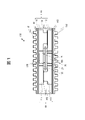
- FIG. 1 is a cross-sectional view of a power semiconductor device 100. This cross-sectional view is a cross-sectional view taken along line XX in a perspective view of the power semiconductor device 100 shown in FIG. 4 described later.
- the power semiconductor device 100 comprises a first upper arm circuit body 110U configured by sandwiching a first switching element 101 constituting an upper arm circuit between a first conductor 111 and a second conductor 112, and a second lower arm circuit constituting the lower arm circuit. It includes a first lower arm circuit body 110L configured by sandwiching the switching element 102 between the third conductor 113 and the fourth conductor 114.
- the positive electrode of the first switching element 101 is bonded to the first conductor 111 by solder or the like, and the negative electrode is bonded to the second conductor 112 by solder or the like.
- the first conductor 111 and the second conductor 112 are made of a conductor such as copper or aluminum.
- the positive electrode of the second switching element 102 is joined to the third conductor 113 by solder or the like, and the negative electrode is joined to the fourth conductor 114 by solder or the like.
- the third conductor 113 and the fourth conductor 114 are made of a conductor such as copper or aluminum.
- the substrate 120 is arranged between the first upper arm circuit body 110U and the first lower arm circuit body 110L.
- the substrate 120 is insulating and is made of resin or ceramic.
- the positive electrode wiring 121 connected to the first conductor 111 on the high potential side and the fourth conductor 114 connected to the low potential side are connected.
- the negative electrode wiring 122 is provided.
- the output wiring 123 connected to the second conductor 112 and the third conductor 113 facing the positive electrode wiring 121 and the negative electrode wiring 122 is provided. It is provided. That is, the positive electrode wiring 121, the negative electrode wiring 122, and the output wiring 123 are laminated on the front and back surfaces of the substrate 120.
- the positive electrode wiring 121, the negative electrode wiring 122, and the output wiring 123 are adhered to the substrate 120, and a pattern is formed on the substrate 120 by etching or the like.
- An output terminal conductor 125 is connected to the output wiring 123.
- the first conductor 111 is joined to the positive conductor wiring 121 by solder or the like
- the second conductor 112 is joined to the output wiring 123 by solder or the like
- the third conductor 113 is joined to the output wiring 123 by solder or the like.
- the conductor 114 is joined to the negative electrode wiring 122 by solder or the like.
- the first capacitor 130 is arranged between the first upper arm circuit body 110U and the first lower arm circuit body 110L, and the terminal on the positive electrode side of the first capacitor 130 is connected to the positive electrode wiring 121 on the substrate 120 and the first capacitor.
- the terminal on the negative electrode side of 130 is joined to the negative electrode wiring 122 on the substrate 120 by solder or the like.
- the first capacitor 130 smoothes the DC power supplied to the first upper arm circuit body 110U and the first lower arm circuit body 110L.
- a small one having high heat resistance such as a ceramic capacitor or a film capacitor is used.
- the gaps between the first upper arm circuit body 110U, the first lower arm circuit body 110L, the substrate 120, and the first capacitor 130 are filled with mold resin. That is, the first upper arm circuit body 110U, the first lower arm circuit body 110L, the substrate 120, and the first capacitor 130 are sealed with a mold resin.
- a first cooler 151 is provided on the surface of the first conductor 111 and the fourth conductor 114 opposite to the surface facing the first switching element 101 and the second switching element 102 via an insulator 141. Although only the cooling fins are shown in the first cooler 151, the cooling fins are covered with a housing (not shown), and a refrigerant such as air or cooling water flows inside.
- a second cooler 152 is provided on the surface of the second conductor 112 and the third conductor 113 opposite to the surface facing the first switching element 101 and the second switching element 102 via an insulator 142. Although only the cooling fins are shown in the second cooler 152, the cooling fins are covered with a housing (not shown), and a refrigerant such as air or cooling water flows inside.
- the insulators 141 and 142 are made of a ceramic or resin sheet.
- a thermal paste layer such as silicon grease may be added to both sides or one side of the insulators 141 and 142.
- the cooling fins of the first cooler 151 and the second cooler 152 are made of a material having high thermal conductivity such as copper and aluminum. The surface area of the first cooler 151 and the second cooler 152 can be increased by forming cooling fins and irregularities, and the cooling performance can be improved.
- the upper surface of the first capacitor 130 is set lower than the upper surfaces of the first conductor 111 and the fourth conductor 114.
- the insulator 141 is provided in close contact with the upper surfaces of the first conductor 111 and the fourth conductor 114, and the first cooler 151 is further provided via the insulator 141, but the upper surface of the first capacitor 130 and the insulator are provided.
- a gap is provided between 141. Therefore, even if the lower surface of the first cooler 151 has some irregularities, the first cooler 151 can be brought into close contact with the upper surfaces of the first conductor 111 and the fourth conductor 114 without being interfered by the first capacitor 130. .. This facilitates the formation of the first cooler 151 and improves the cooling performance.
- the gap between the upper surface of the first capacitor 130 and the insulator 141 is filled with a mold resin.
- the first upper arm circuit body 110U, the first capacitor 130 on the substrate 120, and the first lower arm circuit body 110L are arranged side by side in a straight line.
- the positive electrode wiring 121 and the negative electrode wiring 122 are provided on the front surface of the substrate 120, and the output wiring 123 is provided on the back surface of the substrate 120. To be provided.
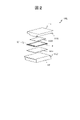
- FIG. 2 is an exploded perspective view of a main part of the first upper arm circuit body 110U of the power semiconductor device 100.
- the control signal wiring 124 is derived from the gate electrode of the first switching element 101.
- the upper surface of the first switching element 101 is an emitter electrode, and the lower surface of the first switching element 101 is a collector electrode.
- the emitter electrode of the first switching element 101 is joined to the first conductor 111 via a bonding material 101D such as solder.
- the collector electrode of the first switching element 101 is joined to the second conductor 112 via the joining material 101D.
- the first conductor 111 has a connection terminal 111E connected to the positive electrode wiring 121 on the substrate 120.
- the second conductor 112 has a connection terminal 112C connected to the output wiring 123 on the substrate 120.
- the connection terminal 111E and the connection terminal 112C and the positive electrode wiring 121 and the output wiring 123 on the substrate 120 are joined to each other in a wide area.
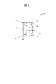
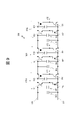
- FIG. 3 is a circuit configuration diagram of the power semiconductor device 100.
- the power semiconductor device 100 is a first arranged in parallel between the first switching element 101 constituting the upper arm circuit, the second switching element 102 constituting the lower arm circuit, and the upper arm circuit and the lower arm circuit.
- a capacitor 130 is provided.
- the positive electrode wiring 121 is connected to the upper arm circuit
- the negative electrode wiring 122 is connected to the lower arm circuit
- the connection point between the first switching element 101 and the second switching element 102 is connected to the output wiring 123.
- the power semiconductor device 100 further constitutes an upper arm circuit, a third switching element 103 connected in parallel with the first switching element 101, and a lower arm circuit, and is connected in parallel with the second switching element 102.
- the fourth switching element 104 and the second capacitor 131 arranged in parallel between the upper arm circuit and the lower arm circuit are provided.
- the positive electrode wiring 121 is connected to the upper arm circuit
- the negative electrode wiring 122 is connected to the lower arm circuit
- the connection point between the third switching element 103 and the fourth switching element 104 is connected to the output wiring 123.
- the control signal wiring 124 (see FIG. 2), which is not shown, is derived from the gate electrodes of the first switching element 101 and the fourth switching element 104, respectively.
- the first switching element 101 and the fourth switching element 104 are power semiconductor elements composed of IGBTs, MOSFETs, or the like.
- the second switching element 102 and the third switching element 103 are diodes.
- the circuit configuration diagram shown in FIG. 3 illustrates one phase of the power semiconductor device 100 used as an inverter for driving a motor.
- the power semiconductor device 100 may be configured with at least the first switching element 101, the second switching element 102, and the first capacitor 130 as one phase.
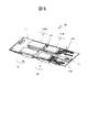
- FIG. 4 is a perspective view of the surface of the substrate 120 of the power semiconductor device 100.
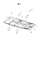
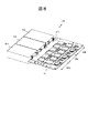
- FIG. 5 is a perspective view of the back surface of the substrate 120 of the power semiconductor device 100.
- the first upper arm circuit body 110U on which the first switching element 101 is mounted is connected in series with the first lower arm circuit body 110L on which the second switching element 102 is mounted via an output wiring 123 provided on the substrate 120. ing.
- the second upper arm circuit body 210U on which the third switching element 103 is mounted is connected in series with the second lower arm circuit body 210L on which the fourth switching element 104 is mounted via the output wiring 123 provided on the substrate 120. ing.
- the first upper arm circuit body 110U on which the first switching element 101 is mounted is connected in parallel to the second upper arm circuit body 210U on which the third switching element 103 is mounted via wiring provided on the substrate 120. ..
- the first lower arm circuit body 110L on which the second switching element 102 is mounted is connected in parallel with the second lower arm circuit body 210L on which the fourth switching element 104 is mounted via wiring provided on the substrate 120. ..
- the first capacitor 130 is arranged between the first upper arm circuit body 110U and the first lower arm circuit body 110L. Further, as shown in FIG. 5, the second capacitor 131 is arranged between the second upper arm circuit body 210U and the second lower arm circuit body 210L. Further, the negative electrode wiring 122 is led out to the front surface of the substrate 120 as shown in FIG. 4, and the positive electrode wiring 121 is led out to the back surface of the substrate 120 as shown in FIG.
- control signal wiring 124 of the first switching element 101 constituting the first upper arm circuit body 101U and the control signal wiring 124 of the fourth switching element 104 constituting the second lower arm circuit body 210L are substrates.
- the 120s are arranged on the same surface so as to face the same direction. As a result, wire bonding to the control signal wiring 124 can be easily performed.
- FIG. 6 is a wiring diagram of the surface of the substrate 120 of the power semiconductor device 100.
- FIG. 7 is a wiring diagram of the back surface of the substrate 120 of the power semiconductor device 100.
- the substrate 120 is provided with through holes 110UH and 110LH in which the first upper arm circuit body 110U and the first lower arm circuit body 110L are arranged, respectively, and further, the second upper arm circuit body 210U and the second lower arm circuit body. Through holes 210UH and 210LH in which 210L are arranged are provided.
- a positive electrode wiring 121, a negative electrode wiring 122, an output wiring 123, and a control signal wiring 124 are patterned on the insulating layer of the substrate 120 by etching or the like.
- a through-hole via 126 is provided on the substrate 120, and the wirings of the positive electrode wiring 121, the negative electrode wiring 122, the output wiring 123, and the control signal wiring 124 are connected between the front surface and the back surface of the substrate 120.
- the positive electrode and the negative electrode of the first capacitor 130 are connected to the positive electrode wiring 121 and the negative electrode wiring 122.
- the positive electrode wiring 121 and the negative electrode wiring 122 are formed in a wide area, and can be joined in a wide area when connected to the first capacitor 130, the first conductor 111, and the fourth conductor 114.
- the positive electrode and the negative electrode of the second capacitor 131 are connected to the positive electrode wiring 121 and the negative electrode wiring 122.
- the positive electrode wiring 121 and the negative electrode wiring 122 are formed in a wide area, and similarly, when connecting to the second capacitor 131 or the like, they can be joined in a wide area.
- control signal wiring 124 is arranged so as to face the same surface of the substrate 120 and face the same direction. Further, a wiring terminal 127 to which a third capacitor 310, which will be described later, is connected is arranged on the substrate 120.
- the power semiconductor device to which this embodiment does not apply does not include a capacitor in the power semiconductor device. Therefore, the wiring path from the switching element in the power semiconductor device to the capacitor outside the power semiconductor device becomes long, and the inductance of the wiring path cannot be reduced.
- the power semiconductor device 100 since the power semiconductor device 100 also includes a capacitor, the wiring path from the switching element to the capacitor can be shortened, and the inductance of the wiring path can be reduced.
- the positive electrode wiring 121 and the negative electrode wiring 122 on the front surface of the substrate 120 and the output wiring 123 on the back surface of the substrate 120 are laminated, in other words, are provided so as to face each other.
- the positive electrode wiring 121, the first upper arm circuit body 110U, the output wiring 123, the first lower arm circuit body 110L, the negative electrode wiring 122, and the first capacitor 130 are opposite to each other.
- the direction in which this current flows through the output wiring 123 on the back surface of the substrate 120 and the direction in which this current flows through the negative electrode wiring 122 on the front surface of the substrate 120 are opposite to each other.
- the magnetic flux can be reduced and the inductance can be reduced by canceling the magnetic flux generated by the flowing current.
- the positive electrode wiring 121, the negative electrode wiring 122, the output wiring 123, and the first capacitor 130 and the first conductors 111 to the fourth conductor 114 are joined to each other in a wide area. Therefore, since the above-mentioned currents flowing in opposite directions are in a wide range, the canceling magnetic flux can be increased and the inductance can be reduced more effectively.
- FIG. 8 is a perspective view of the power conversion device 300.
- the power conversion device 300 is configured as an inverter for driving a motor by using the power semiconductor device 100 described in the first embodiment.
- power semiconductor devices 100U, 100V, and 100W are used as the U-phase, V-phase, and W-phase of the inverter corresponding to the three-phase motor.
- the power semiconductor devices 100U, 100V, and 100W have the same configuration as the power semiconductor device 100 described in the first embodiment. However, in the present embodiment, the power semiconductor devices 100U, 100V, and 100W are configured on one substrate 120.
- the third capacitor 310 is connected to the wiring terminal 127 of the substrate 120.
- the third capacitor 310 is a large-capacity smoothing capacitor, is composed of a film capacitor or the like, and is connected in parallel with the first capacitor 130 and the second capacitor 131.
- the inverter composed of the power semiconductor devices 100U, 100V, and 100W converts the DC power supplied from the battery or the like into AC power to drive the motor.
- the third capacitor 310 has a lower heat resistant temperature than the first capacitor 130 and the second capacitor 131, but has a larger capacity.
- the first capacitor 130 and the second capacitor 131 are arranged close to the upper and lower arm circuits, and the wiring length thereof is shortened to reduce the inductance of the wiring path, and the third capacitor 310 is connected in parallel to have a large capacity. It is possible to suppress the DC voltage fluctuation due to the change.
- FIG. 9 is a circuit configuration diagram of the power conversion device 300.
- the power semiconductor devices 100U, 100V, and 100W have the same configuration as the power semiconductor device 100 described with reference to FIG.
- the DC wiring that is, the third capacitor 310 is connected between the positive electrode wiring 121 and the negative electrode wiring 122.
- the power semiconductor devices 100U, 100V, and 100W are connected in parallel between the positive electrode wiring 121 and the negative electrode wiring 122.
- FIG. 10 is an exploded perspective view of the electric system 600.
- the electric system 600 includes a power conversion device 300, a motor 400, and a gear 500.
- the power conversion device 300 includes the configuration described with reference to FIGS. 8 and 9.
- the third capacitor 310 does not necessarily have to be provided.
- the power conversion device 300 converts DC power supplied from a battery or the like into AC power, and its output wiring 123 is connected to the winding of the motor 400 to drive the motor 400.
- the motor 400 is driven by using the AC power output from the power conversion device 300. Then, a rotational torque is generated in the output shaft 401.
- the gear 500 is connected to the output shaft 401 of the motor 400 to change the rotation speed of the output shaft 401.
- the power conversion device 300, the motor 400, and the gear 500 are integrally fastened by screws or the like.
- the first upper arm circuit body 110U configured by sandwiching the first switching element 101 constituting the upper arm circuit between the first conductor 111 and the second conductor 112, and the second switching element 102 constituting the lower arm circuit.
- the power semiconductor device 100 provided with the first lower arm circuit body 110L configured by sandwiching the third conductor 113 and the fourth conductor 114, the power semiconductor device 100 has a high potential side on one surface.
- a positive conductor 121 connected to one conductor 111 and a negative conductor 122 connected to a fourth conductor 114 on the low potential side are provided, and a second conductor is provided on the other surface so as to face the positive conductor 121 and the negative conductor 122.
- the substrate 120 provided with the output wiring 123 connected to the conductor 112 and the third conductor 113, and the first capacitor 130 for smoothing the DC power supplied to the first upper arm circuit body 110U and the first lower arm circuit body 110L.
- the substrate 120 is arranged between the first upper arm circuit body 110U and the first lower arm circuit body 110L, and the first capacitor 130 is the first upper arm circuit body 110U and the first lower arm circuit. It is arranged between the body 110L and connected to the positive electrode wiring 121 and the negative electrode wiring 122 on the substrate 120. This makes it possible to reduce the inductance of the wiring path.
- the present invention is not limited to the above-described embodiment, and other embodiments considered within the scope of the technical idea of the present invention are also included within the scope of the present invention as long as the features of the present invention are not impaired. .. Further, the configuration may be a combination of the above-described embodiments.
- Control signal wiring 126 ... Through hole via, 127 ... Wiring terminal, 130 ... 1st capacitor, 131 ... 2nd capacitor, 141 , 142 ... insulator, 151 ... first cooler, 152 ... second cooler, 300 ... power converter, 310 ... third capacitor, 400 ... motor, 401. ⁇ ⁇ Output shaft, 500 ⁇ ⁇ ⁇ Gear, 600 ⁇ ⁇ ⁇ Electric system.
Landscapes
- Engineering & Computer Science (AREA)
- Power Engineering (AREA)
- Physics & Mathematics (AREA)
- Electromagnetism (AREA)
- Microelectronics & Electronic Packaging (AREA)
- Inverter Devices (AREA)
Abstract
一方の面に、高電位側である前記第1導体に接続される正極配線と低電位側である第4導体に接続される負極配線とを設け、他方の面に、前記正極配線および前記負極配線と対向して、第2導体および第3導体に接続される出力配線を設けた基板と、第1上アーム回路体および第1下アーム回路体へ供給される直流電力を平滑化する第1キャパシタと、を備え、前記基板は、前記第1上アーム回路体と前記第1下アーム回路体との間に配置され、前記第1キャパシタは、前記第1上アーム回路体と前記第1下アーム回路体との間に配置され、かつ前記基板上の前記正極配線および前記負極配線に接続されるパワー半導体装置。
Description
本発明は、パワー半導体装置、電力変換装置、および電動システムに関する。
電力変換装置は、直流電力を平滑化するキャパシタと直流電流を交流電流に変換するスイッチング素子とを備えて構成される。そして、スイッチング素子のスイッチングの際には電流の急激な変化に伴って配線経路のインダクタンスに比例したサージ電圧が発生するため、配線経路のインダクタンスの低減が求められる。
特許文献1には、上アームおよび下アームを3相分備えた三相インバータ回路を構成する半導体モジュールにおいて、多層配線バスバーを備え、多層配線バスバーには、出力配線層が3相それぞれの上アームと下アームの中間電位点と接続されるU相配線層とV相配線層およびW相配線層とを積層して構成された半導体モジュールが開示されている。
特許文献1の装置では、キャパシタまでも含めた配線経路は考慮されておらず、配線経路が長くなり、配線経路のインダクタンスを低減することができない。
本発明によるパワー半導体装置は、上アーム回路を構成する第1スイッチング素子を第1導体および第2導体により挟んで構成される第1上アーム回路体と、下アーム回路を構成する第2スイッチング素子を第3導体および第4導体により挟んで構成される第1下アーム回路体とを備えたパワー半導体装置において、一方の面に、高電位側である前記第1導体に接続される正極配線と低電位側である前記第4導体に接続される負極配線とを設け、他方の面に、前記正極配線および前記負極配線と対向して、前記第2導体および前記第3導体に接続される出力配線を設けた基板と、前記第1上アーム回路体および前記第1下アーム回路体へ供給される直流電力を平滑化する第1キャパシタと、を備え、前記基板は、前記第1上アーム回路体と前記第1下アーム回路体との間に配置され、前記第1キャパシタは、前記第1上アーム回路体と前記第1下アーム回路体との間に配置され、かつ前記基板上の前記正極配線および前記負極配線に接続される。
本発明によれば、配線経路のインダクタンスを低減することができる。
以下、図面を参照して本発明の実施形態を説明する。以下の記載および図面は、本発明を説明するための例示であって、説明の明確化のため、適宜、省略および簡略化がなされている。本発明は、他の種々の形態でも実施する事が可能である。特に限定しない限り、各構成要素は単数でも複数でも構わない。
図面において示す各構成要素の位置、大きさ、形状、範囲などは、発明の理解を容易にするため、実際の位置、大きさ、形状、範囲などを表していない場合がある。このため、本発明は、必ずしも、図面に開示された位置、大きさ、形状、範囲などに限定されない。
同一あるいは同様な機能を有する構成要素が複数ある場合には、同一の符号に異なる添字を付して説明する場合がある。ただし、これらの複数の構成要素を区別する必要がない場合には、添字を省略して説明する場合がある。
[第1の実施形態]
図1は、パワー半導体装置100の断面図である。この断面図は、後述の図4に示すパワー半導体装置100の斜視図におけるX-X線の断面図である。
図1は、パワー半導体装置100の断面図である。この断面図は、後述の図4に示すパワー半導体装置100の斜視図におけるX-X線の断面図である。
パワー半導体装置100は、上アーム回路を構成する第1スイッチング素子101を第1導体111および第2導体112により挟んで構成される第1上アーム回路体110Uと、下アーム回路を構成する第2スイッチング素子102を第3導体113および第4導体114により挟んで構成される第1下アーム回路体110Lとを備える。
第1スイッチング素子101の正極は、第1導体111とはんだ等によって接合され、負極は、第2導体112とはんだ等によって接合される。第1導体111と第2導体112は、銅やアルミなどの導体で構成されている。
第2スイッチング素子102の正極は、第3導体113とはんだ等によって接合され、負極は、第4導体114とはんだ等によって接合される。第3導体113と第4導体114は、銅やアルミなどの導体で構成されている。
第1上アーム回路体110Uと第1下アーム回路体110Lとの間には基板120が配置される。基板120は、絶縁性であり、樹脂やセラミックで構成されている。
基板120の一方の面(図の上面であり、以下、表面と称する)に、高電位側である第1導体111に接続される正極配線121と、低電位側である第4導体114に接続される負極配線122とを設けている。基板120の他方の面(図の下面であり、以下、裏面と称する)に、正極配線121および負極配線122と対向して、第2導体112および第3導体113に接続される出力配線123を設けている。すなわち、正極配線121および負極配線122と出力配線123とは基板120の表裏において積層されている。正極配線121、負極配線122、および出力配線123は、基板120に接着されており、基板120にエッチングなどによりパターン形成される。出力配線123には出力端子導体125が接続されている。
第1導体111は、正極配線121とはんだ等によって接合され、第2導体112は、出力配線123とはんだ等によって接合され、第3導体113は、出力配線123とはんだ等によって接合され、第4導体114は、負極配線122とはんだ等によって接合されている。
第1キャパシタ130は、第1上アーム回路体110Uと第1下アーム回路体110Lとの間に配置され、第1キャパシタ130の正極側の端子は基板120上の正極配線121に、第1キャパシタ130の負極側の端子は基板120上の負極配線122にはんだ等により接合される。第1キャパシタ130は、第1上アーム回路体110Uおよび第1下アーム回路体110Lへ供給される直流電力を平滑化する。第1キャパシタ130は、セラミックコンデンサまたはフィルムコンデンサなど、小型で耐熱性の高いものが用いられる。
第1上アーム回路体110U、第1下アーム回路体110L、基板120、および第1キャパシタ130の隙間は、モールド樹脂が充填されている。すなわち、第1上アーム回路体110U、第1下アーム回路体110L、基板120、および第1キャパシタ130は、モールド樹脂により封止されている。
第1導体111および第4導体114の第1スイッチング素子101および第2スイッチング素子102と対向する面と反対の面には絶縁体141を介して第1冷却器151が設けられている。第1冷却器151は冷却フィンのみを図示しているが、図示省略した筐体によって冷却フィンが覆われ、内部に空気や冷却水などの冷媒が流通する。
第2導体112および第3導体113の第1スイッチング素子101および第2スイッチング素子102と対向する面と反対の面には絶縁体142を介して第2冷却器152が設けられている。第2冷却器152は冷却フィンのみを図示しているが、図示省略した筐体によって冷却フィンが覆われ、内部に空気や冷却水などの冷媒が流通する。
絶縁体141、142は、セラミックや樹脂シートにより構成される。絶縁体141、142の両面または片面にシリコングリスなど放熱グリス層を追加してもよい。
第1冷却器151、第2冷却器152の冷却フィンは、銅やアルミなど熱伝導性の高い材料で構成される。第1冷却器151、第2冷却器152は、冷却フィンや凹凸を形成することで表面積を増大させ、冷却性能を向上させることができる。
第1冷却器151、第2冷却器152の冷却フィンは、銅やアルミなど熱伝導性の高い材料で構成される。第1冷却器151、第2冷却器152は、冷却フィンや凹凸を形成することで表面積を増大させ、冷却性能を向上させることができる。
第1キャパシタ130の上面は、第1導体111および第4導体114の上面よりも低く設定される。換言すれば、第1導体111および第4導体114の上面に密着して絶縁体141が、さらに絶縁体141を介して第1冷却器151が設けられるが、第1キャパシタ130の上面と絶縁体141の間には間隙を設ける。このため、第1冷却器151の下面に多少の凹凸があったとしても、第1キャパシタ130の干渉を受けることなく第1導体111および第4導体114の上面に第1冷却器151を密着できる。これにより第1冷却器151の形成が容易になり、冷却性能も向上する。なお、第1キャパシタ130の上面と絶縁体141との間隙にはモールド樹脂が充填される。
本実施形態では、第1上アーム回路体110U、基板120上の第1キャパシタ130、第1下アーム回路体110Lが直線状に並んで配置している。そして、正極配線121および負極配線122を基板120の表面に、出力配線123を基板120の裏面に設け、すなわち、正極配線121および負極配線122と出力配線123とを対向して、換言すると積層して設ける。
図2は、パワー半導体装置100の第1上アーム回路体110Uの要部分解斜視図である。
第1スイッチング素子101のゲート電極から制御信号配線124が導出される。第1スイッチング素子101の図示上面がエミッタ電極であり、図示下面がコレクタ電極である。第1スイッチング素子101のエミッタ電極は、図1では図示を省略したが、はんだ等の接合材101Dを介して、第1導体111に接合される。第1スイッチング素子101のコレクタ電極は、接合材101Dを介して、第2導体112に接合される。
第1スイッチング素子101のゲート電極から制御信号配線124が導出される。第1スイッチング素子101の図示上面がエミッタ電極であり、図示下面がコレクタ電極である。第1スイッチング素子101のエミッタ電極は、図1では図示を省略したが、はんだ等の接合材101Dを介して、第1導体111に接合される。第1スイッチング素子101のコレクタ電極は、接合材101Dを介して、第2導体112に接合される。
第1導体111は、基板120上の正極配線121に接続される接続端子111Eを有する。第2導体112は、基板120上の出力配線123に接続される接続端子112Cを有する。ここで、接続端子111E、および接続端子112Cと、基板120上の正極配線121および出力配線123とは互いに広い面積で接合される。
図3は、パワー半導体装置100の回路構成図である。
パワー半導体装置100は、上アーム回路を構成する第1スイッチング素子101と、下アーム回路を構成する第2スイッチング素子102と、上アーム回路と下アーム回路との間に並列に配置される第1キャパシタ130を備える。正極配線121は上アーム回路に、負極配線122は下アーム回路に接続され、第1スイッチング素子101と第2スイッチング素子102の接続点は出力配線123に接続される。
パワー半導体装置100は、上アーム回路を構成する第1スイッチング素子101と、下アーム回路を構成する第2スイッチング素子102と、上アーム回路と下アーム回路との間に並列に配置される第1キャパシタ130を備える。正極配線121は上アーム回路に、負極配線122は下アーム回路に接続され、第1スイッチング素子101と第2スイッチング素子102の接続点は出力配線123に接続される。
パワー半導体装置100は、さらに、上アーム回路を構成し、第1スイッチング素子101と並列に接続される第3スイッチング素子103と、下アーム回路を構成し、第2スイッチング素子102と並列に接続される第4スイッチング素子104と、上アーム回路と下アーム回路との間に並列に配置される第2キャパシタ131を備える。正極配線121は上アーム回路に、負極配線122は下アーム回路に接続され、第3スイッチング素子103と第4スイッチング素子104の接続点は出力配線123に接続される。
第1スイッチング素子101および第4スイッチング素子104のゲート電極から夫々図示省略した制御信号配線124(図2参照)が導出される。
第1スイッチング素子101および第4スイッチング素子104は、IGBTまたはMOSFETなどで構成されるパワー半導体素子である。第2スイッチング素子102および第3スイッチング素子103は、ダイオードである。
第1スイッチング素子101および第4スイッチング素子104は、IGBTまたはMOSFETなどで構成されるパワー半導体素子である。第2スイッチング素子102および第3スイッチング素子103は、ダイオードである。
図3に示した回路構成図は、モータを駆動するインバータとして用いるパワー半導体装置100の1相分を図示したものである。この場合、パワー半導体装置100は、少なくとも、第1スイッチング素子101と、第2スイッチング素子102と、第1キャパシタ130とを1相分として構成してもよい。
図4は、パワー半導体装置100の基板120の表面の斜視図である。図5は、パワー半導体装置100の基板120の裏面の斜視図である。これらの図では、第1冷却器151、第2冷却器152を取り除いた状態を示す。
第1スイッチング素子101が搭載された第1上アーム回路体110Uは、基板120に設けられた出力配線123を介して第2スイッチング素子102が搭載された第1下アーム回路体110Lと直列接続されている。
第3スイッチング素子103が搭載された第2上アーム回路体210Uは、基板120に設けられた出力配線123を介して第4スイッチング素子104が搭載された第2下アーム回路体210Lと直列接続されている。
第1スイッチング素子101が搭載された第1上アーム回路体110Uは、基板120に設けられた配線を介して第3スイッチング素子103が搭載された第2上アーム回路体210Uと並列接続されている。第2スイッチング素子102が搭載された第1下アーム回路体110Lは、基板120に設けられた配線を介して第4スイッチング素子104が搭載された第2下アーム回路体210Lと並列接続されている。
図4に示すように、第1キャパシタ130は、第1上アーム回路体110Uと第1下アーム回路体110Lとの間に配置される。また、図5に示すように、第2キャパシタ131は、第2上アーム回路体210Uと第2下アーム回路体210Lとの間に配置される。
また、負極配線122は、図4に示すように、基板120の表面に導出され、正極配線121は、図5に示すように、基板120の裏面に導出される。
また、負極配線122は、図4に示すように、基板120の表面に導出され、正極配線121は、図5に示すように、基板120の裏面に導出される。
図5に示すように、第1上アーム回路体101Uを構成する第1スイッチング素子101の制御信号配線124および第2下アーム回路体210Lを構成する第4スイッチング素子104の制御信号配線124は基板120の同一面に同一方向を向くように配置される。これにより、制御信号配線124に対するワイヤーボンディングを容易に行うことができる。
図6は、パワー半導体装置100の基板120の表面の配線図である。図7は、パワー半導体装置100の基板120の裏面の配線図である。
基板120には、第1上アーム回路体110U、第1下アーム回路体110Lがそれぞれ配置される貫通孔110UH、110LHが設けられ、さらに、第2上アーム回路体210Uと第2下アーム回路体210Lが配置される貫通孔210UH、210LHが設けられている。
基板120には、第1上アーム回路体110U、第1下アーム回路体110Lがそれぞれ配置される貫通孔110UH、110LHが設けられ、さらに、第2上アーム回路体210Uと第2下アーム回路体210Lが配置される貫通孔210UH、210LHが設けられている。
基板120の絶縁層の上には、正極配線121、負極配線122、出力配線123、制御信号配線124がエッチングなどによりパターン形成される。基板120には、スルーホールビア126が設けられ、正極配線121、負極配線122、出力配線123、制御信号配線124の各配線同士が基板120の表面と裏面の間で接続されている。
図6に示す基板120の表面の貫通孔110UHと貫通孔110LHの間であって、正極配線121、負極配線122に第1キャパシタ130の正極と負極が接続される。ここで、正極配線121、負極配線122は広い面積で形成されており、第1キャパシタ130、第1導体111、第4導体114との接続に際しては、広い面積で接合することができる。
図7に示す基板120の裏面の貫通孔210UHと貫通孔210LHの間であって、正極配線121、負極配線122に第2キャパシタ131の正極と負極が接続される。ここで、正極配線121、負極配線122は広い面積で形成されており、同様に第2キャパシタ131等との接続に際しては、広い面積で接合することができる。
また、図7に示すように、制御信号配線124は基板120の同一面に同一方向を向くように配置される。また、基板120には、後述の第3キャパシタ310が接続される配線端子127が配置されている。
本実施形態を適用しないパワー半導体装置は、パワー半導体装置にキャパシタを内包していない。このため、パワー半導体装置内のスイッチング素子からパワー半導体装置外のキャパシタまでの配線経路が長くなって、配線経路のインダクタンスを低減することができなかった。
これに対して、本実施形態では、パワー半導体装置100にキャパシタも内包しているので、スイッチング素子からキャパシタまでの配線経路を短くすることができ、配線経路のインダクタンスを低減することができる。
加えて、本実施形態では、基板120の表面の正極配線121および負極配線122と基板120の裏面の出力配線123とは積層して、換言すれば対向して、設けている。ここで、図1を参照して、第1キャパシタ130の正極から正極配線121、第1上アーム回路体110U、出力配線123、第1下アーム回路体110L、負極配線122、そして第1キャパシタ130の負極へ流れる電流に注目する。この電流が、基板120の表面の正極配線121を流れる方向と、基板120の裏面の出力配線123を流れる方向とは互いに逆方向になる。同様に、この電流が、基板120の裏面の出力配線123を流れる方向と、基板120の表面の負極配線122を流れる方向とは互いに逆方向になる。これにより、流れる電流によって発生する磁束を相殺することにより、磁束が減少し、インダクタンスを低減することができる。
さらに、正極配線121、負極配線122、出力配線123と、第1キャパシタ130や第1導体111~第4導体114とは互いに広い面積で接合される。したがって、上述した互いに逆方向に流れる電流は幅広い領域になるので、相殺する磁束を増加させて、より効果的にインダクタンスを低減することができる。
[第2の実施形態]
図8は、電力変換装置300の斜視図である。
電力変換装置300は、第1の実施形態で述べたパワー半導体装置100を用いて、モータを駆動するインバータとして構成したものである。
図8は、電力変換装置300の斜視図である。
電力変換装置300は、第1の実施形態で述べたパワー半導体装置100を用いて、モータを駆動するインバータとして構成したものである。
図8に示すように、三相のモータに対応してインバータのU相、V相、W相としてパワー半導体装置100U、100V、100Wを用いる。パワー半導体装置100U、100V、100Wは第1の実施形態で述べたパワー半導体装置100と同一の構成である。ただし、本実施形態では、一枚の基板120にパワー半導体装置100U、100V、100Wを構成する。さらに、第3キャパシタ310を基板120の配線端子127に接続する。第3キャパシタ310は、大容量平滑コンデンサであり、フィルムコンデンサ等によって構成され、第1キャパシタ130、第2キャパシタ131と並列に接続される。
パワー半導体装置100U、100V、100Wにより構成されたインバータは、バッテリなどから供給される直流電力を交流電力に変換し、モータを駆動する。
第3キャパシタ310は、第1キャパシタ130、第2キャパシタ131よりも耐熱温度は低いが容量は大きい。第1キャパシタ130、第2キャパシタ131を上下アーム回路体に近接して配置し、その配線長を短くすることにより配線路の低インダクタンス化を図るとともに、第3キャパシタ310を並列接続して大容量化することによる直流電圧変動を抑制することができる。
第3キャパシタ310は、第1キャパシタ130、第2キャパシタ131よりも耐熱温度は低いが容量は大きい。第1キャパシタ130、第2キャパシタ131を上下アーム回路体に近接して配置し、その配線長を短くすることにより配線路の低インダクタンス化を図るとともに、第3キャパシタ310を並列接続して大容量化することによる直流電圧変動を抑制することができる。
図9は、電力変換装置300の回路構成図である。
パワー半導体装置100U、100V、100Wは、図3を参照して説明したパワー半導体装置100と同一の構成である。本実施形態では、直流配線、すなわち、正極配線121と負極配線122との間に、第3キャパシタ310が接続される。そして、パワー半導体装置100U、100V、100Wが正極配線121と負極配線122との間に並列に接続される。
パワー半導体装置100U、100V、100Wは、図3を参照して説明したパワー半導体装置100と同一の構成である。本実施形態では、直流配線、すなわち、正極配線121と負極配線122との間に、第3キャパシタ310が接続される。そして、パワー半導体装置100U、100V、100Wが正極配線121と負極配線122との間に並列に接続される。
図10は、電動システム600の分解斜視図である。
電動システム600は、電力変換装置300、モータ400、ギア500よりなる。
電力変換装置300は、図8、図9を参照して説明した構成を備える。なお、第3キャパシタ310は必ずしも備えなくてもよい。電力変換装置300は、バッテリなどから供給される直流電力を交流電力に変換し、その出力配線123はモータ400の巻線に接続され、モータ400を駆動する。
電動システム600は、電力変換装置300、モータ400、ギア500よりなる。
電力変換装置300は、図8、図9を参照して説明した構成を備える。なお、第3キャパシタ310は必ずしも備えなくてもよい。電力変換装置300は、バッテリなどから供給される直流電力を交流電力に変換し、その出力配線123はモータ400の巻線に接続され、モータ400を駆動する。
モータ400は、電力変換装置300から出力される交流電力を用いて駆動される。そして、出力軸401に回転トルクを発生させる。
ギア500は、モータ400の出力軸401に連結されて、出力軸401の回転数を変速する。電力変換装置300、モータ400、ギア500はビス等により締結されて一体的に構成される。
ギア500は、モータ400の出力軸401に連結されて、出力軸401の回転数を変速する。電力変換装置300、モータ400、ギア500はビス等により締結されて一体的に構成される。
以上説明した実施形態によれば、次の作用効果が得られる。
(1)上アーム回路を構成する第1スイッチング素子101を第1導体111および第2導体112により挟んで構成される第1上アーム回路体110Uと、下アーム回路を構成する第2スイッチング素子102を第3導体113および第4導体114により挟んで構成される第1下アーム回路体110Lとを備えたパワー半導体装置100において、パワー半導体装置100は、一方の面に、高電位側である第1導体111に接続される正極配線121と低電位側である第4導体114に接続される負極配線122とを設け、他方の面に、正極配線121および負極配線122と対向して、第2導体112および第3導体113に接続される出力配線123を設けた基板120と、第1上アーム回路体110Uおよび第1下アーム回路体110Lへ供給される直流電力を平滑化する第1キャパシタ130と、を備え、基板120は、第1上アーム回路体110Uと第1下アーム回路体110Lとの間に配置され、第1キャパシタ130は、第1上アーム回路体110Uと第1下アーム回路体110Lとの間に配置され、かつ基板120上の正極配線121および負極配線122に接続される。これにより、配線経路のインダクタンスを低減することができる。
(1)上アーム回路を構成する第1スイッチング素子101を第1導体111および第2導体112により挟んで構成される第1上アーム回路体110Uと、下アーム回路を構成する第2スイッチング素子102を第3導体113および第4導体114により挟んで構成される第1下アーム回路体110Lとを備えたパワー半導体装置100において、パワー半導体装置100は、一方の面に、高電位側である第1導体111に接続される正極配線121と低電位側である第4導体114に接続される負極配線122とを設け、他方の面に、正極配線121および負極配線122と対向して、第2導体112および第3導体113に接続される出力配線123を設けた基板120と、第1上アーム回路体110Uおよび第1下アーム回路体110Lへ供給される直流電力を平滑化する第1キャパシタ130と、を備え、基板120は、第1上アーム回路体110Uと第1下アーム回路体110Lとの間に配置され、第1キャパシタ130は、第1上アーム回路体110Uと第1下アーム回路体110Lとの間に配置され、かつ基板120上の正極配線121および負極配線122に接続される。これにより、配線経路のインダクタンスを低減することができる。
本発明は、上述の実施形態に限定されるものではなく、本発明の特徴を損なわない限り、本発明の技術思想の範囲内で考えられるその他の形態についても、本発明の範囲内に含まれる。また、上述の実施形態を組み合わせた構成としてもよい。
100、100U、100V、100W・・・パワー半導体装置、101・・・第1スイッチング素子、101D・・・接合材、102・・・第2スイッチング素子、103・・・第3スイッチング素子、104・・・第4スイッチング素子、110U・・・第1上アーム回路体、110L・・・第1下アーム回路体、110UH、110LH、210UH、210LH・・・貫通孔、111・・・第1導体、111E、112C・・・接続端子、112・・・第2導体、113・・・第3導体、114・・・第4導体、120・・・基板、121・・・正極配線、122・・・負極配線、123・・・出力配線、124・・・制御信号配線、126・・・スルーホールビア、127・・・配線端子、130・・・第1キャパシタ、131・・・第2キャパシタ、141、142・・・絶縁体、151・・・第1冷却器、152・・・第2冷却器、300・・・電力変換装置、310・・・第3キャパシタ、400・・・モータ、401・・・出力軸、500・・・ギア、600・・・電動システム。
Claims (8)
- 上アーム回路を構成する第1スイッチング素子を第1導体および第2導体により挟んで構成される第1上アーム回路体と、下アーム回路を構成する第2スイッチング素子を第3導体および第4導体により挟んで構成される第1下アーム回路体とを備えたパワー半導体装置において、
一方の面に、高電位側である前記第1導体に接続される正極配線と低電位側である前記第4導体に接続される負極配線とを設け、他方の面に、前記正極配線および前記負極配線と対向して、前記第2導体および前記第3導体に接続される出力配線を設けた基板と、
前記第1上アーム回路体および前記第1下アーム回路体へ供給される直流電力を平滑化する第1キャパシタと、を備え、
前記基板は、前記第1上アーム回路体と前記第1下アーム回路体との間に配置され、
前記第1キャパシタは、前記第1上アーム回路体と前記第1下アーム回路体との間に配置され、かつ前記基板上の前記正極配線および前記負極配線に接続されるパワー半導体装置。 - 請求項1に記載のパワー半導体装置において、
前記第1導体および前記第4導体の第1スイッチング素子および第2スイッチング素子と対向する面と反対の面には絶縁体を介して第1冷却器が設けられ、
前記第2導体および前記第3導体の第1スイッチング素子および第2スイッチング素子と対向する面と反対の面には絶縁体を介して第2冷却器が設けられたパワー半導体装置。 - 請求項1または請求項2に記載のパワー半導体装置において、
前記第1キャパシタの上面は、前記第1導体および前記第4導体の上面よりも低く設定されるパワー半導体装置。 - 請求項1に記載のパワー半導体装置において、
前記第1スイッチング素子と並列に接続される第3スイッチング素子を備える第2上アーム回路体と、前記第2スイッチング素子と並列に接続される第4スイッチング素子を備える第2下アーム回路体と、前記第2上アーム回路体および前記第2下アーム回路体へ供給される直流電力を平滑化する第2キャパシタと、を備え、
前記第2キャパシタは、前記第2上アーム回路体と前記第2下アーム回路体との間に配置され、かつ前記基板上の前記正極配線および前記負極配線に接続されるパワー半導体装置。 - 請求項4に記載のパワー半導体装置において、
前記第1上アーム回路体と前記第1下アーム回路体の配列および前記第2上アーム回路体と前記第2下アーム回路体の配列は互いに並列であり、
前記第1上アーム回路体を構成する前記第1スイッチング素子の制御信号配線および前記第2下アーム回路体を構成する前記第4スイッチング素子の制御信号配線は同一方向を向くパワー半導体装置。 - 請求項4に記載のパワー半導体装置を直流配線によって並列に複数個接続した電力変換装置。
- 請求項6に記載の電力変換装置において、
前記パワー半導体装置の各々に対応して前記直流配線に第3キャパシタを設けた電力変換装置。 - 請求項6または請求項7に記載の電力変換装置と、
前記電力変換装置から出力される交流電力を用いて駆動されるモータと、
前記モータの出力軸に連結されて、前記出力軸の回転数を変速するギアとを一体的に設けた電動システム。
Priority Applications (3)
| Application Number | Priority Date | Filing Date | Title |
|---|---|---|---|
| US18/034,305 US12581947B2 (en) | 2020-10-30 | 2021-09-17 | Power semiconductor device, power conversion device, and electric system |
| DE112021004521.0T DE112021004521T5 (de) | 2020-10-30 | 2021-09-17 | Leistungshalbleitervorrichtung, leistungsumsetzungsvorrichtung und elektrisches system |
| CN202180072655.8A CN116420304B (zh) | 2020-10-30 | 2021-09-17 | 功率半导体装置、功率转换装置和电动系统 |
Applications Claiming Priority (2)
| Application Number | Priority Date | Filing Date | Title |
|---|---|---|---|
| JP2020183263A JP6968967B1 (ja) | 2020-10-30 | 2020-10-30 | パワー半導体装置、電力変換装置、および電動システム |
| JP2020-183263 | 2020-10-30 |
Publications (1)
| Publication Number | Publication Date |
|---|---|
| WO2022091633A1 true WO2022091633A1 (ja) | 2022-05-05 |
Family
ID=78605593
Family Applications (1)
| Application Number | Title | Priority Date | Filing Date |
|---|---|---|---|
| PCT/JP2021/034314 Ceased WO2022091633A1 (ja) | 2020-10-30 | 2021-09-17 | パワー半導体装置、電力変換装置、および電動システム |
Country Status (4)
| Country | Link |
|---|---|
| US (1) | US12581947B2 (ja) |
| JP (1) | JP6968967B1 (ja) |
| DE (1) | DE112021004521T5 (ja) |
| WO (1) | WO2022091633A1 (ja) |
Families Citing this family (1)
| Publication number | Priority date | Publication date | Assignee | Title |
|---|---|---|---|---|
| JP7853854B2 (ja) * | 2022-07-14 | 2026-04-30 | 住友重機械工業株式会社 | インバータ装置、電源装置 |
Citations (5)
| Publication number | Priority date | Publication date | Assignee | Title |
|---|---|---|---|---|
| JPH10304680A (ja) * | 1997-04-25 | 1998-11-13 | Toyota Motor Corp | 電力変換装置 |
| JP2009225612A (ja) * | 2008-03-18 | 2009-10-01 | Mitsubishi Electric Corp | パワーモジュール |
| WO2012073571A1 (ja) * | 2010-12-01 | 2012-06-07 | 株式会社安川電機 | 電力変換装置 |
| JP2013252009A (ja) * | 2012-06-01 | 2013-12-12 | Toyota Motor Corp | スナバコンデンサが搭載された半導体モジュールの保護回路 |
| JP2015039295A (ja) * | 2010-11-02 | 2015-02-26 | 三菱電機株式会社 | 電動式パワーステアリング用パワーモジュールおよびこれを用いた電動式パワーステアリング駆動制御装置 |
Family Cites Families (4)
| Publication number | Priority date | Publication date | Assignee | Title |
|---|---|---|---|---|
| JP2002359329A (ja) * | 2001-05-30 | 2002-12-13 | Hitachi Ltd | 半導体装置 |
| JP5481148B2 (ja) * | 2009-10-02 | 2014-04-23 | 日立オートモティブシステムズ株式会社 | 半導体装置、およびパワー半導体モジュール、およびパワー半導体モジュールを備えた電力変換装置 |
| JP6269296B2 (ja) | 2014-04-25 | 2018-01-31 | 株式会社デンソー | 半導体モジュール |
| JP7135930B2 (ja) * | 2019-02-20 | 2022-09-13 | 株式会社デンソー | 半導体モジュールとそれを用いた電力変換装置 |
-
2020
- 2020-10-30 JP JP2020183263A patent/JP6968967B1/ja active Active
-
2021
- 2021-09-17 DE DE112021004521.0T patent/DE112021004521T5/de active Pending
- 2021-09-17 US US18/034,305 patent/US12581947B2/en active Active
- 2021-09-17 WO PCT/JP2021/034314 patent/WO2022091633A1/ja not_active Ceased
Patent Citations (5)
| Publication number | Priority date | Publication date | Assignee | Title |
|---|---|---|---|---|
| JPH10304680A (ja) * | 1997-04-25 | 1998-11-13 | Toyota Motor Corp | 電力変換装置 |
| JP2009225612A (ja) * | 2008-03-18 | 2009-10-01 | Mitsubishi Electric Corp | パワーモジュール |
| JP2015039295A (ja) * | 2010-11-02 | 2015-02-26 | 三菱電機株式会社 | 電動式パワーステアリング用パワーモジュールおよびこれを用いた電動式パワーステアリング駆動制御装置 |
| WO2012073571A1 (ja) * | 2010-12-01 | 2012-06-07 | 株式会社安川電機 | 電力変換装置 |
| JP2013252009A (ja) * | 2012-06-01 | 2013-12-12 | Toyota Motor Corp | スナバコンデンサが搭載された半導体モジュールの保護回路 |
Also Published As
| Publication number | Publication date |
|---|---|
| US12581947B2 (en) | 2026-03-17 |
| US20230395457A1 (en) | 2023-12-07 |
| JP2022073334A (ja) | 2022-05-17 |
| DE112021004521T5 (de) | 2023-09-21 |
| JP6968967B1 (ja) | 2021-11-24 |
| CN116420304A (zh) | 2023-07-11 |
Similar Documents
| Publication | Publication Date | Title |
|---|---|---|
| CN102414816B (zh) | 功率模块及电力转换装置 | |
| CN101681898B (zh) | 半导体元件的冷却构造 | |
| US9307666B2 (en) | Electric circuit device, electric circuit module, and power converter | |
| CN104506050B (zh) | 电力转换装置 | |
| CN116325135B (zh) | 半导体封装、半导体装置以及电力变换装置 | |
| CN101795054B (zh) | 电力变换装置 | |
| JP3723869B2 (ja) | 半導体装置 | |
| JP5830480B2 (ja) | 配線板およびそれを用いた電力変換装置 | |
| JP6977682B2 (ja) | 回転電機ユニット | |
| WO2023058381A1 (ja) | 電力変換装置 | |
| WO2014030458A1 (ja) | パワー半導体モジュール | |
| JP6447914B2 (ja) | パワーモジュールの直流側配線基板及びその製造方法 | |
| JP7760399B2 (ja) | 半導体装置 | |
| JP3673776B2 (ja) | 半導体モジュール及び電力変換装置 | |
| JP7410005B2 (ja) | モータと一緒に共有した冷却システムを有した高密度一体型電源制御アセンブリ | |
| JP6968967B1 (ja) | パワー半導体装置、電力変換装置、および電動システム | |
| JP7693094B2 (ja) | パワーモジュール半導体パッケージおよび半導体装置 | |
| JP3972855B2 (ja) | インバータモジュール | |
| WO2022107439A1 (ja) | パワー半導体モジュール | |
| JP7836718B2 (ja) | 電力変換装置 | |
| WO2025211108A1 (ja) | 電力変換装置 | |
| WO2026014232A1 (ja) | 半導体装置 | |
| WO2026014233A1 (ja) | 半導体装置 | |
| WO2026014234A1 (ja) | 半導体装置 | |
| WO2025033118A1 (ja) | 半導体装置および電力変換装置 |
Legal Events
| Date | Code | Title | Description |
|---|---|---|---|
| 121 | Ep: the epo has been informed by wipo that ep was designated in this application |
Ref document number: 21885752 Country of ref document: EP Kind code of ref document: A1 |
|
| WWE | Wipo information: entry into national phase |
Ref document number: 112021004521 Country of ref document: DE |
|
| 122 | Ep: pct application non-entry in european phase |
Ref document number: 21885752 Country of ref document: EP Kind code of ref document: A1 |
|
| WWG | Wipo information: grant in national office |
Ref document number: 18034305 Country of ref document: US |