WO2022085319A1 - 磁気センサパッケージ - Google Patents
磁気センサパッケージ Download PDFInfo
- Publication number
- WO2022085319A1 WO2022085319A1 PCT/JP2021/032819 JP2021032819W WO2022085319A1 WO 2022085319 A1 WO2022085319 A1 WO 2022085319A1 JP 2021032819 W JP2021032819 W JP 2021032819W WO 2022085319 A1 WO2022085319 A1 WO 2022085319A1
- Authority
- WO
- WIPO (PCT)
- Prior art keywords
- magnetic sensor
- sensor chip
- wiring layer
- sensor package
- connection
- Prior art date
- Legal status (The legal status is an assumption and is not a legal conclusion. Google has not performed a legal analysis and makes no representation as to the accuracy of the status listed.)
- Ceased
Links
Images










Classifications
-
- G—PHYSICS
- G01—MEASURING; TESTING
- G01R—MEASURING ELECTRIC VARIABLES; MEASURING MAGNETIC VARIABLES
- G01R33/00—Arrangements or instruments for measuring magnetic variables
- G01R33/02—Measuring direction or magnitude of magnetic fields or magnetic flux
- G01R33/06—Measuring direction or magnitude of magnetic fields or magnetic flux using galvano-magnetic devices
-
- H—ELECTRICITY
- H10—SEMICONDUCTOR DEVICES; ELECTRIC SOLID-STATE DEVICES NOT OTHERWISE PROVIDED FOR
- H10W—GENERIC PACKAGES, INTERCONNECTIONS, CONNECTORS OR OTHER CONSTRUCTIONAL DETAILS OF DEVICES COVERED BY CLASS H10
- H10W70/00—Package substrates; Interposers; Redistribution layers [RDL]
- H10W70/60—Insulating or insulated package substrates; Interposers; Redistribution layers
-
- H—ELECTRICITY
- H10—SEMICONDUCTOR DEVICES; ELECTRIC SOLID-STATE DEVICES NOT OTHERWISE PROVIDED FOR
- H10W—GENERIC PACKAGES, INTERCONNECTIONS, CONNECTORS OR OTHER CONSTRUCTIONAL DETAILS OF DEVICES COVERED BY CLASS H10
- H10W74/00—Encapsulations, e.g. protective coatings
- H10W74/10—Encapsulations, e.g. protective coatings characterised by their shape or disposition
-
- H—ELECTRICITY
- H10—SEMICONDUCTOR DEVICES; ELECTRIC SOLID-STATE DEVICES NOT OTHERWISE PROVIDED FOR
- H10W—GENERIC PACKAGES, INTERCONNECTIONS, CONNECTORS OR OTHER CONSTRUCTIONAL DETAILS OF DEVICES COVERED BY CLASS H10
- H10W74/00—Encapsulations, e.g. protective coatings
- H10W74/40—Encapsulations, e.g. protective coatings characterised by their materials
Definitions
- the present invention relates to a magnetic sensor package.
- Patent Document 1 Japanese Patent Application Laid-Open No. 2018-11995
- the magnetic field sensor described in Patent Document 1 includes a magnetic field sensing element disposed in the first surface of the die and a solder ball in contact with the second surface of the die. Through silicon vias penetrate the die to connect the magnetic field sensing element and the solder ball to each other.
- the present invention has been made in view of the above problems, and is to reduce the stress transmitted to the magnetic detection element from the connection point with the substrate when mounted on the substrate to maintain high magnetic detection accuracy.
- the purpose is to provide a magnetic sensor package that can be used.
- the magnetic sensor package based on the present invention includes a magnetic sensor chip, a connection wiring layer, a columnar electrode, an insulating layer, and a connection electrode.
- the magnetic sensor chip has a first surface provided with connection terminals.
- a magnetic detection element is arranged along the first surface.
- the connection wiring layer is electrically connected to the connection terminal and extends along the first surface to the outside of the edge of the magnetic sensor chip when viewed from a direction orthogonal to the first surface.
- the columnar electrode is electrically connected to the connecting wiring layer at a position outside the edge of the magnetic sensor chip when viewed from the direction orthogonal to the first surface, and is spaced along the magnetic sensor chip along the magnetic sensor chip. It is postponed.
- the insulating layer covers the first surface while being in contact with the surface of the connection wiring layer opposite to the surface on the magnetic sensor chip side.
- the connection electrode is electrically connected to the end surface of the columnar electrode opposite to the connection wiring layer side.
- the present invention it is possible to maintain high magnetic detection accuracy by reducing the stress transmitted to the magnetic detection element from the connection point with the board when mounted on the board.
- FIG. 3 is a plan view of the magnetic sensor package of FIG. 1 as viewed from the direction of the arrow along line II-II. It is the bottom view which looked at the magnetic sensor package of FIG. 1 from the direction of arrow III. It is a top view which shows the 1st surface of the magnetic sensor provided in the magnetic sensor package which concerns on Embodiment 1 of this invention. It is a figure which shows the circuit structure of the magnetic sensor chip provided in the magnetic sensor package which concerns on Embodiment 1 of this invention.
- FIG. 3 is a vertical cross-sectional view showing a state in which a printed wiring board is resin-molded in the method for manufacturing a magnetic sensor package according to the first embodiment of the present invention. It is a vertical sectional view which shows the state which the mold resin part was ground together with the magnetic sensor chip and the columnar electrode in the manufacturing method of the magnetic sensor package which concerns on Embodiment 1 of this invention.
- FIG. 3 is a vertical sectional view showing a state in which a connection electrode is formed on an end surface of a columnar electrode opposite to the connection wiring layer side in the method for manufacturing a magnetic sensor package according to the first embodiment of the present invention.
- FIG. 12 is a plan view of the magnetic sensor package of FIG. 12 as viewed from the direction of arrow XIII. It is the bottom view which looked at the magnetic sensor package of FIG. 12 from the direction of arrow XIV.
- FIG. 3 is a vertical sectional view showing a state in which a connection wiring layer and an insulating layer are formed after the adhesive sheet is peeled off and the support substrate is removed in the method for manufacturing a magnetic sensor package according to the second embodiment of the present invention.
- FIG. 3 is a vertical sectional view showing a state in which a connection electrode is formed on an end surface of a columnar electrode opposite to the connection wiring layer side in the method for manufacturing a magnetic sensor package according to the second embodiment of the present invention. It is sectional drawing which shows the structure of the magnetic sensor package which concerns on Embodiment 3 of this invention. It is a vertical sectional view which shows the state which the magnetic sensor chip and the columnar electrode are mounted on the support substrate provided with the adhesive sheet in the manufacturing method of the magnetic sensor package which concerns on Embodiment 3 of this invention. It is a vertical sectional view which shows the state which resin-molded on the support substrate in the manufacturing method of the magnetic sensor package which concerns on Embodiment 3 of this invention.
- FIG. 3 is a vertical sectional view showing a state in which a connection wiring layer and an insulating layer are formed after the adhesive sheet is peeled off and the support substrate is removed in the method for manufacturing a magnetic sensor package according to the third embodiment of the present invention.
- FIG. 3 is a vertical sectional view showing a state in which a connection electrode is formed on an end surface of a columnar electrode opposite to the connection wiring layer side in the method for manufacturing a magnetic sensor package according to the third embodiment of the present invention.
- FIG. 25 is a bottom view of the magnetic sensor package of FIG. 25 as viewed from the direction of arrow XXVI. It is a vertical sectional view which shows the state which the magnetic sensor chip and the columnar electrode are mounted on the support substrate provided with the adhesive sheet in the manufacturing method of the magnetic sensor package which concerns on Embodiment 4 of this invention. It is a vertical sectional view which shows the state which resin-molded on the support substrate in the manufacturing method of the magnetic sensor package which concerns on Embodiment 4 of this invention.
- FIG. 25 is a bottom view of the magnetic sensor package of FIG. 25 as viewed from the direction of arrow XXVI. It is a vertical sectional view which shows the state which the magnetic sensor chip and the columnar electrode are mounted on the support substrate provided with the adhesive sheet in the manufacturing method of the magnetic sensor package which concerns on Embodiment 4 of this invention. It is a vertical sectional view which shows the state which resin-molded on the support substrate in the manufacturing method of the magnetic sensor package which concerns on Embodiment 4 of this invention.
- FIG. 5 is a vertical sectional view showing a state in which a connection wiring layer and an insulating layer are formed after the adhesive sheet is peeled off and the support substrate is removed in the method for manufacturing a magnetic sensor package according to the fourth embodiment of the present invention.
- FIG. 3 is a vertical sectional view showing a state in which an extension wiring layer is formed on an end surface of a columnar electrode opposite to the connection wiring layer side in the method for manufacturing a magnetic sensor package according to the fourth embodiment of the present invention. It is a vertical cross-sectional view which shows the state which formed the connection electrode on the extension wiring layer in the manufacturing method of the magnetic sensor package which concerns on Embodiment 2 of this invention.
- FIG. 1 is a cross-sectional view showing the configuration of the magnetic sensor package according to the first embodiment of the present invention.
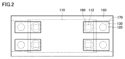
- FIG. 2 is a plan view of the magnetic sensor package of FIG. 1 as viewed from the direction of the arrow along line II-II.
- FIG. 3 is a bottom view of the magnetic sensor package of FIG. 1 as viewed from the direction of arrow III.
- the magnetic sensor package 100 includes a magnetic sensor chip 110, a connection wiring layer 120, a columnar electrode 130, an insulating layer 150, and a connection electrode 140. And.
- the magnetic sensor chip 110 has a rectangular parallelepiped shape.
- the magnetic sensor chip 110 has a first surface 111, a second surface 113 opposite to the first surface 111, and a peripheral surface connecting the first surface 111 and the second surface 113 to each other.
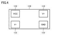
- FIG. 4 is a plan view showing the first surface of the magnetic sensor included in the magnetic sensor package according to the first embodiment of the present invention.
- four connection terminals 112 are provided on the first surface 111 of the magnetic sensor chip 110.
- the four connection terminals 112 are arranged one by one at the four corners of the first surface 111 of the magnetic sensor chip 110.
- the four connection terminals 112 are composed of a power supply terminal Vcc, a ground terminal GND, a first output terminal V +, and a second output terminal V-.
- the magnetic sensor chip 110 a magnetic detection element is arranged along the first surface 111.
- the magnetic sensor chip 110 includes a sensor substrate made of silicon, glass, ceramic, or the like, and a magnetic detection element and four connection terminals 112 are formed on the sensor substrate.
- the magnetic detection element is covered with a protective layer made of, for example, SiO 2 . An opening is formed in the protective layer of the portion located above each of the four connection terminals 112.
- the magnetic detection element is a TMR (Tunnel Magneto Resistance) element, but the magnetic detection element is not limited to the TMR element, and is an AMR (Anisotropic Magneto Resistance) element, a GMR (Giant Magneto Resistance) element, or the like. It may be a magnetoresistive element or a Hall element.
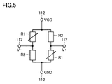
- FIG. 5 is a diagram showing a circuit configuration of a magnetic sensor chip included in the magnetic sensor package according to the first embodiment of the present invention.
- the magnetic sensor chip 110 has a Wheatstone bridge type bridge circuit including four TMR elements. Specifically, two series connectors of the variable resistor R1 and the fixed resistor R2 are connected in parallel between the power supply terminal Vcc and the ground terminal GND.
- the first output terminal V + is connected to the connection point between the fixed resistor R2 and the variable resistor R1.
- the second output terminal V- is connected to the connection point between the variable resistor R1 and the fixed resistor R2.
- the resistance value of the variable resistor R1 becomes smaller when the magnetic field to be detected acts on it.
- the resistance value of the fixed resistance R2 hardly decreases even when the magnetic field to be detected acts on it.
- the magnetic sensor chip 110 Since the magnetic sensor chip 110 has the above circuit configuration, a potential difference depending on the strength of the magnetic field to be detected is generated between the first output terminal V + and the second output terminal V-.
- the magnetic sensor chip 110 may have a half-bridge circuit including one variable resistor R1 and one fixed resistor R2.
- connection wiring layer 120 is electrically connected to the connection terminal 112, and is an edge of the magnetic sensor chip 110 along the first surface 111 and when viewed from a direction orthogonal to the first surface 111. It extends to the outside.
- the four connection wiring layers 120 are electrically connected to the four connection terminals 112 in a one-to-one correspondence.
- two of the four connection wiring layers 120 are orthogonal to one side of the edge of the magnetic sensor chip 110, and the remaining two are orthogonal to each other.
- the connection wiring layer 120 is orthogonal to the other side located parallel to the one side.
- connection wiring layer 120 has a rectangular parallelepiped shape.
- shape of the connection wiring layer 120 when viewed from a direction orthogonal to the first surface 111 is not limited to a rectangle, and may be an ellipse or the like.
- the connection wiring layer 120 is provided on the surface of the insulating layer 150 on the magnetic sensor chip side.
- the insulating layer 150 and the connecting wiring layer 120 are formed of a printed wiring board.
- connection wiring layer 120 The portion of the connection wiring layer 120 facing the connection terminal 112 is electrically connected to each other by the connection conductor 180.
- the connection wiring layer 120 is made of a conductive material such as gold or copper.
- the connecting conductor 180 is made of a conductive material such as solder or gold.
- the columnar electrode 130 is electrically connected to the connection wiring layer 120 at a position outside the edge of the magnetic sensor chip 110 when viewed from a direction orthogonal to the first surface 111, and the magnetic sensor is spaced apart from the magnetic sensor chip 110. It extends along the peripheral surface of the chip 110.
- the four columnar electrodes 130 are electrically connected to the four connection wiring layers 120 in a one-to-one correspondence.
- the columnar electrode 130 has a columnar shape.
- the shape of the columnar electrode 130 is not limited to the columnar shape, and may be a prismatic shape.
- the columnar electrode 130 is connected to the surface of the connection wiring layer 120 on the magnetic sensor chip side.
- the end surface of the columnar electrode 130 opposite to the connection wiring layer side is located on substantially the same plane as the second surface 113 of the magnetic sensor chip 110.
- the columnar electrode 130 is made of a conductive material such as gold or copper.
- the insulating layer 150 covers the first surface 111 of the magnetic sensor chip 110 while being in contact with the surface of the connection wiring layer 120 opposite to the surface on the magnetic sensor chip side.
- the surface of the insulating layer 150 on the magnetic sensor chip side and the first surface 111 face each other with a gap from each other.
- the thickness dimension of the insulating layer 150 is 20 ⁇ m or less.
- the portion located around the columnar electrode 130 is covered with the solder resist 170. That is, each part of the insulating layer 150 and the connecting wiring layer 120 is covered with the solder resist 170.
- the thickness dimension of the solder resist 170 is 20 ⁇ m or less.
- the distance between the surface of the insulating layer 150 opposite to the magnetic sensor chip side, which is the surface of the magnetic sensor package, and the magnetic detection element is 50 ⁇ m or less.
- the insulating layer 150 is formed of a glass epoxy substrate.
- the material constituting the insulating layer 150 is not limited to this, and may be a thermosetting resin such as an epoxy resin, a phenol resin, a melamine resin or a urethane resin, or a resin composition containing a thermosetting resin.
- connection electrode 140 is electrically connected to the end surface of the columnar electrode 130 opposite to the connection wiring layer side.
- the connection electrode 140 is made of a conductive material such as solder or gold.
- the magnetic sensor package 100 further includes a mold resin portion 160 that covers at least the peripheral surface of the magnetic sensor chip 110.
- the mold resin portion 160 fills a portion between the position on the surface of the insulating layer 150 on the magnetic sensor chip side and the position of the second surface 113 of the magnetic sensor chip 110 in the direction orthogonal to the first surface 111. ..
- the second surface 113 is a ground surface that has been ground.
- the end face of the columnar electrode 130 opposite to the connection wiring layer side is not covered with the mold resin portion 160.
- the mold resin portion 160 is made of a thermosetting molding material in which a silica filler or the like is added to a main component such as an epoxy resin.
- FIG. 6 is a vertical cross-sectional view showing a state in which a columnar electrode is formed on a printed wiring board in the method for manufacturing a magnetic sensor package according to the first embodiment of the present invention.
- a columnar electrode 130 is formed by plating on a printed wiring board including an insulating layer 150 and a connecting wiring layer 120.
- the columnar electrode 130 may be mounted on the connection wiring layer 120.
- the surface of the insulating layer 150 opposite to the connection wiring layer side is covered with the solder resist 190.
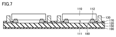
- FIG. 7 is a vertical sectional view showing a state in which a magnetic sensor chip is mounted on a printed wiring board in the method for manufacturing a magnetic sensor package according to the first embodiment of the present invention.
- the magnetic sensor chip 110 is flip-chip mounted on the printed wiring board so that the connection terminal 112 of the magnetic sensor chip 110 and the connection wiring layer 120 are electrically connected via the connection conductor 180. do.
- FIG. 8 is a vertical cross-sectional view showing a state in which a printed wiring board is resin-molded in the method for manufacturing a magnetic sensor package according to the first embodiment of the present invention. As shown in FIG. 8, the magnetic sensor chip 110 on the printed wiring board is embedded in the mold resin portion 160.
- FIG. 9 is a vertical sectional view showing a state in which the molded resin portion is ground together with the magnetic sensor chip and the columnar electrode in the method for manufacturing the magnetic sensor package according to the first embodiment of the present invention.
- the magnetic sensor is ground by grinding the mold resin portion 160 from the side opposite to the insulating layer side and also grinding the sides of the magnetic sensor chip 110 and the columnar electrode 130 opposite to the insulating layer side. Each of the second surface 113 of the chip 110 and the end face of the columnar electrode 130 opposite to the connection wiring layer side is exposed.
- FIG. 10 is a vertical cross-sectional view showing a state in which the insulating layer is ground in the method for manufacturing a magnetic sensor package according to the first embodiment of the present invention. As shown in FIG. 10, the solder resist 190 and the insulating layer 150 of the printed wiring board are ground to remove the solder resist 190 and thin the insulating layer 150.
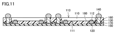
- FIG. 11 is a vertical cross-sectional view showing a state in which a connection electrode is formed on an end surface of a columnar electrode opposite to the connection wiring layer side in the method for manufacturing a magnetic sensor package according to the first embodiment of the present invention.
- the connection electrode 140 is formed on the end surface of the columnar electrode 130 opposite to the connection wiring layer side by a plating method, a vapor deposition method, or a printing method.
- the magnetic sensor package 100 shown in FIG. 1 can be manufactured by individualizing it by dicing or the like.
- the magnetic sensor chip 110 has a first surface 111 provided with a connection terminal 112.
- a magnetic detection element is arranged along the first surface 111.
- the connection wiring layer 120 is electrically connected to the connection terminal 112 and extends along the first surface 111 to the outside of the edge of the magnetic sensor chip 110 when viewed from a direction orthogonal to the first surface 111.
- the columnar electrode 130 is electrically connected to the connection wiring layer 120 at a position outside the edge of the magnetic sensor chip 110 when viewed from a direction orthogonal to the first surface 111, and the magnetic sensor is spaced apart from the magnetic sensor chip 110. It extends along the chip 110.
- the insulating layer 150 covers the first surface 111 while being in contact with the surface of the connection wiring layer 120 opposite to the surface on the magnetic sensor chip side.
- the connection electrode 140 is electrically connected to the end surface of the columnar electrode 130 opposite to the connection wiring layer side.
- the magnetic detection element is arranged along the first surface 111 of the magnetic sensor chip 110.
- the distance from the surface of the magnetic sensor package 100 to the magnetic detection element is reduced to 50 ⁇ m or less, and the magnetic sensor package
- the magnetic detection accuracy for a magnetic field near the surface of 100 can be increased.
- connection electrode 140 which is a connection point with the substrate
- the stress transmission path to the detection element can be lengthened, and the stress transmitted to the magnetic detection element can be reduced to maintain high magnetic detection accuracy.
- the columnar electrode 130 is arranged outside the magnetic sensor chip 110, it is possible to suppress the magnetic field generated around the columnar electrode 130 due to the current flowing through the columnar electrode 130 from acting on the magnetic detection element. .. This also allows the magnetic sensor package 100 to maintain high magnetic detection accuracy.
- the insulating layer 150 and the connection wiring layer 120 are formed of a printed wiring board. This makes it possible to manufacture the magnetic sensor package 100 by a simple manufacturing method.
- the second surface 113 of the magnetic sensor chip 110 is a ground surface and is exposed from the mold resin portion 160. As a result, the magnetic sensor package 100 can be made thinner.
- the magnetic sensor package according to the second embodiment of the present invention is different from the magnetic sensor package 100 according to the first embodiment of the present invention in that the insulating layer is mainly composed of a thin film. The description of the configuration similar to that of the magnetic sensor package 100 according to the first embodiment will not be repeated.
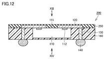
- FIG. 12 is a cross-sectional view showing the configuration of the magnetic sensor package according to the second embodiment of the present invention.
- FIG. 13 is a plan view of the magnetic sensor package of FIG. 12 as viewed from the direction of arrow XIII.
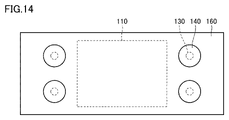
- FIG. 14 is a bottom view of the magnetic sensor package of FIG. 12 as viewed from the direction of arrow XIV. In FIG. 13, the insulating layer is shown through.
- the magnetic sensor package 200 includes a magnetic sensor chip 110, a connection wiring layer 120, a columnar electrode 130, an insulating layer 250, and a connection electrode 140. And.
- connection wiring layer 120 extends from the top of the first surface 111 of the magnetic sensor chip 110 to the outside of the edge of the magnetic sensor chip 110 along the first surface 111.
- the connection terminal 112 of the magnetic sensor chip 110 and the connection wiring layer 120 are directly connected to each other.
- the insulating layer 250 covers the first surface 111 of the magnetic sensor chip 110 while being in contact with the surface of the connection wiring layer 120 opposite to the surface on the magnetic sensor chip side.
- the insulating layer 250 covers the entire surface of the connection wiring layer 120 opposite to the surface on the magnetic sensor chip side.
- the surface of the insulating layer 250 on the magnetic sensor chip side and the first surface 111 are in direct contact with each other.
- the dimension of the thickness of the insulating layer 150 located on the first surface 111 is 10 ⁇ m or less.
- the distance between the surface of the insulating layer 250 opposite to the magnetic sensor chip side, which is the surface of the magnetic sensor package, and the magnetic detection element is 20 ⁇ m or less.
- the entire magnetic sensor chip 110 is embedded in the mold resin portion 160.
- FIG. 15 is a vertical sectional view showing a state in which a magnetic sensor chip and a columnar electrode are mounted on a support substrate provided with an adhesive sheet in the method for manufacturing a magnetic sensor package according to the second embodiment of the present invention.
- the magnetic sensor chip 110 and the columnar electrode 130 are mounted on the support substrate 290 provided with the adhesive sheet 291.
- the first surface 111 of the magnetic sensor chip 110 is in direct contact with the adhesive sheet 291.
- the columnar electrode 130 may be formed by plating on the adhesive sheet 291.
- FIG. 16 is a vertical sectional view showing a state in which a support substrate is resin-molded in the method for manufacturing a magnetic sensor package according to the first embodiment of the present invention.
- the magnetic sensor chip 110 and the columnar electrode 130 on the support substrate 290 are embedded in the mold resin portion 160.
- the end face of the columnar electrode 130 opposite to the support substrate side is exposed.
- the mold resin portion 160 may be molded so that the end face of the columnar electrode 130 is exposed, or the columnar electrode 130 may be molded so as to be embedded in the mold resin portion 160. After that, the end face of the columnar electrode 130 may be exposed by grinding the mold resin portion 160.
- FIG. 17 is a vertical sectional view showing a state in which a connection wiring layer and an insulating layer are formed after the adhesive sheet is peeled off and the support substrate is removed in the method for manufacturing a magnetic sensor package according to the second embodiment of the present invention. be.
- a film is formed by a sputtering method, a vapor deposition method, or the like, and the connection wiring layer 120 is formed by patterning by a photolithography method.
- the insulating layer 250 is formed by a sputtering method, a vapor deposition method, or the like so as to cover the first surface 111 of the magnetic sensor chip 110 and the connection wiring layer 120.
- the insulating layer 250 is made of SiO 2 or SiN or the like.
- FIG. 18 is a vertical cross-sectional view showing a state in which a connection electrode is formed on an end surface of a columnar electrode opposite to the connection wiring layer side in the method for manufacturing a magnetic sensor package according to the second embodiment of the present invention.
- the connection electrode 140 is formed on the end surface of the columnar electrode 130 on the side opposite to the connection wiring layer side by a plating method, a vapor deposition method, or a printing method.
- the magnetic sensor package 200 shown in FIG. 12 can be manufactured by individualizing it by dicing or the like.
- the insulating layer 250 is composed of a thin film having a thickness of 10 ⁇ m or less, the distance from the surface of the magnetic sensor package 100 to the magnetic detection element is 20 ⁇ m or less. The magnetic detection accuracy for the magnetic field near the surface of the magnetic sensor package 200 can be increased.
- connection electrode 140 which is a connection point with the substrate
- the stress transmission path to the detection element can be lengthened, and the stress transmitted to the magnetic detection element can be reduced to maintain high magnetic detection accuracy.
- the columnar electrode 130 is arranged outside the magnetic sensor chip 110, it is possible to suppress the magnetic field generated around the columnar electrode 130 due to the current flowing through the columnar electrode 130 from acting on the magnetic detection element. .. This also allows the magnetic sensor package 200 to maintain high magnetic detection accuracy.
- the magnetic sensor package according to the third embodiment of the present invention is different from the magnetic sensor package 200 according to the second embodiment of the present invention in that the second surface of the magnetic sensor chip is a ground surface.
- the description of the configuration similar to that of the magnetic sensor package 200 according to the second embodiment will not be repeated.
- FIG. 19 is a cross-sectional view showing the configuration of the magnetic sensor package according to the third embodiment of the present invention. As shown in FIG. 19, in the magnetic sensor package 300 according to the third embodiment of the present invention, only the second surface 113 is not covered with the mold resin portion 160 and is exposed. The second surface 113 is a ground surface that has been ground.
- FIG. 20 is a vertical sectional view showing a state in which a magnetic sensor chip and a columnar electrode are mounted on a support substrate provided with an adhesive sheet in the method for manufacturing a magnetic sensor package according to the third embodiment of the present invention.
- the magnetic sensor chip 110 and the columnar electrode 130 are mounted on the support substrate 290 provided with the adhesive sheet 291.
- the first surface 111 of the magnetic sensor chip 110 is in direct contact with the adhesive sheet 291.
- the columnar electrode 130 may be formed by plating on the adhesive sheet 291.
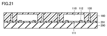
- FIG. 21 is a vertical sectional view showing a state in which a support substrate is resin-molded in the method for manufacturing a magnetic sensor package according to the third embodiment of the present invention. As shown in FIG. 21, the magnetic sensor chip 110 and the columnar electrode 130 on the support substrate 290 are embedded in the mold resin portion 160.
- FIG. 22 is a vertical sectional view showing a state in which the molded resin portion is ground together with the magnetic sensor chip and the columnar electrode in the method for manufacturing the magnetic sensor package according to the third embodiment of the present invention.
- the magnetic sensor is ground by grinding the mold resin portion 160 from the side opposite to the insulating layer side and also grinding the side opposite to the insulating layer side of each of the magnetic sensor chip 110 and the columnar electrode 130.
- Each of the second surface 113 of the chip 110 and the end face of the columnar electrode 130 opposite to the connection wiring layer side is exposed.
- FIG. 23 is a vertical sectional view showing a state in which a connection wiring layer and an insulating layer are formed after the adhesive sheet is peeled off and the support substrate is removed in the method for manufacturing a magnetic sensor package according to the third embodiment of the present invention. be.
- the connection wiring layer 120 is electrically connected to each of the connection terminal 112 and the columnar electrode 130 of the magnetic sensor chip 110.
- a film is formed by a sputtering method or a vapor deposition method, and patterning is performed by a photolithography method.
- the insulating layer 250 is formed by a sputtering method, a vapor deposition method, or the like so as to cover the first surface 111 of the magnetic sensor chip 110 and the connection wiring layer 120.
- FIG. 24 is a vertical cross-sectional view showing a state in which a connection electrode is formed on an end surface of a columnar electrode opposite to the connection wiring layer side in the method for manufacturing a magnetic sensor package according to the third embodiment of the present invention.
- the connection electrode 140 is formed on the end surface of the columnar electrode 130 opposite to the connection wiring layer side by a plating method, a vapor deposition method, or a printing method.
- the magnetic sensor package 300 shown in FIG. 19 can be manufactured by individualizing it by dicing or the like.
- the second surface 113 of the magnetic sensor chip 110 is a ground surface and is exposed from the mold resin portion 160. As a result, the magnetic sensor package 300 can be made thinner.
- the magnetic sensor package according to the fourth embodiment of the present invention is mainly the same as the magnetic sensor package 200 according to the second embodiment of the present invention in that an extension wiring layer is provided between the columnar electrode and the connection electrode. Since they are different, the description of the same configuration as that of the magnetic sensor package 200 according to the second embodiment of the present invention will not be repeated.
- FIG. 25 is a cross-sectional view showing the configuration of the magnetic sensor package according to the fourth embodiment of the present invention.
- FIG. 26 is a bottom view of the magnetic sensor package of FIG. 25 as viewed from the direction of arrow XXVI.
- the magnetic sensor package 400 includes a magnetic sensor chip 110, a connection wiring layer 120, a columnar electrode 130, an insulating layer 250, and a connection electrode 140. And an extension wiring layer 420.
- the extension wiring layer 420 is electrically connected to each of the end surface of the columnar electrode 130 opposite to the connection wiring layer side and the connection electrode 140, and is in a direction along the end surface of the columnar electrode 130 opposite to the connection wiring layer side. It is extended to.
- the extension wiring layer 420 extends along the surface of the mold resin portion 160 opposite to the insulating layer side.
- the columnar electrode 130 and the connection electrode 140 are electrically connected to each other via the extension wiring layer 420.
- FIG. 27 is a vertical sectional view showing a state in which a magnetic sensor chip and a columnar electrode are mounted on a support substrate provided with an adhesive sheet in the method for manufacturing a magnetic sensor package according to the fourth embodiment of the present invention.
- the magnetic sensor chip 110 and the columnar electrode 130 are mounted on the support substrate 290 provided with the adhesive sheet 291.
- the first surface 111 of the magnetic sensor chip 110 is in direct contact with the adhesive sheet 291.
- the columnar electrode 130 may be formed by plating on the adhesive sheet 291.
- FIG. 28 is a vertical cross-sectional view showing a state in which the support substrate is resin-molded in the method for manufacturing a magnetic sensor package according to the fourth embodiment of the present invention.
- the magnetic sensor chip 110 and the columnar electrode 130 on the support substrate 290 are embedded in the mold resin portion 160.
- the end face of the columnar electrode 130 opposite to the support substrate side is exposed.
- the entire magnetic sensor chip 110 is embedded in the mold resin portion 160.
- FIG. 29 is a vertical sectional view showing a state in which a connection wiring layer and an insulating layer are formed after the adhesive sheet is peeled off and the support substrate is removed in the method for manufacturing a magnetic sensor package according to the fourth embodiment of the present invention. be.
- the connection wiring layer 120 is electrically connected to each of the connection terminal 112 and the columnar electrode 130 of the magnetic sensor chip 110.
- a film is formed by a sputtering method or a vapor deposition method, and patterning is performed by a photolithography method.
- the insulating layer 250 is formed by a sputtering method, a vapor deposition method, or the like so as to cover the first surface 111 of the magnetic sensor chip 110 and the connection wiring layer 120.
- FIG. 30 is a vertical cross-sectional view showing a state in which an extension wiring layer is formed on an end surface of a columnar electrode opposite to the connection wiring layer side in the method for manufacturing a magnetic sensor package according to the fourth embodiment of the present invention. ..
- the extension wiring layer 420 is formed by forming a film by a sputtering method, a vapor deposition method, or the like so that the columnar electrode 130 and the extension wiring layer 420 are electrically connected, and patterning the extension wiring layer 420 by a photolithography method. Form.
- FIG. 31 is a vertical cross-sectional view showing a state in which a connection electrode is formed on an extension wiring layer in the method for manufacturing a magnetic sensor package according to the second embodiment of the present invention.
- the connection electrode 140 is formed on the extension wiring layer 420 by a plating method, a vapor deposition method, or a printing method.
- the magnetic sensor package 400 shown in FIG. 25 can be manufactured by individualizing it by dicing or the like.
- the end face of the columnar electrode 130 opposite to the connection wiring layer side and each of the connection electrodes 140 are electrically connected, and the connection wiring layer of the columnar electrode 130 is electrically connected. Further, an extension wiring layer 420 extending in a direction along the end face on the opposite side to the side is provided.
- connection electrode 140 which is a connection point with the substrate
- the stress transmission path from the connection electrode 140 to the magnetic detection element can be lengthened, and the stress transmitted to the magnetic detection element can be reduced to maintain high magnetic detection accuracy.
- connection electrode 140 since the columnar electrode 130 and the connection electrode 140 are electrically connected to each other via the extension wiring layer 420, the formation position of the connection electrode 140 can be adjusted according to the arrangement of the extension wiring layer 420. Therefore, the degree of freedom in the formation position of the connection electrode 140 can be increased.
- 100, 200, 300, 400 magnetic sensor package 110 magnetic sensor chip, 111 first surface, 112 connection terminal, 113 second surface, 120 connection wiring layer, 130 columnar electrode, 140 connection electrode, 150, 250 insulation layer, 160 Mold resin part, 170, 190 solder resist, 180 connection conductor, 290 support board, 291 adhesive sheet, 420 extension wiring layer, 2018 Japanese Patent Laid-Open No., GND ground terminal, R1 variable resistance, R2 fixed resistance, V + 1st output terminal, V -Second output terminal, Vcc power supply terminal.
Landscapes
- Physics & Mathematics (AREA)
- Condensed Matter Physics & Semiconductors (AREA)
- General Physics & Mathematics (AREA)
- Measuring Magnetic Variables (AREA)
- Hall/Mr Elements (AREA)
Priority Applications (1)
| Application Number | Priority Date | Filing Date | Title |
|---|---|---|---|
| JP2022557264A JP7501654B2 (ja) | 2020-10-21 | 2021-09-07 | 磁気センサパッケージ |
Applications Claiming Priority (2)
| Application Number | Priority Date | Filing Date | Title |
|---|---|---|---|
| JP2020176519 | 2020-10-21 | ||
| JP2020-176519 | 2020-10-21 |
Publications (1)
| Publication Number | Publication Date |
|---|---|
| WO2022085319A1 true WO2022085319A1 (ja) | 2022-04-28 |
Family
ID=81291231
Family Applications (1)
| Application Number | Title | Priority Date | Filing Date |
|---|---|---|---|
| PCT/JP2021/032819 Ceased WO2022085319A1 (ja) | 2020-10-21 | 2021-09-07 | 磁気センサパッケージ |
Country Status (2)
| Country | Link |
|---|---|
| JP (1) | JP7501654B2 (https=) |
| WO (1) | WO2022085319A1 (https=) |
Cited By (1)
| Publication number | Priority date | Publication date | Assignee | Title |
|---|---|---|---|---|
| JP7138261B1 (ja) | 2022-06-30 | 2022-09-15 | 旭化成エレクトロニクス株式会社 | 半導体パッケージ、及び駆動装置 |
Citations (4)
| Publication number | Priority date | Publication date | Assignee | Title |
|---|---|---|---|---|
| JPH0579964U (ja) * | 1992-04-03 | 1993-10-29 | 株式会社三協精機製作所 | 磁気センサ |
| JP2017009566A (ja) * | 2015-06-26 | 2017-01-12 | 旭化成エレクトロニクス株式会社 | センサ装置及びセンサ装置の製造方法 |
| JP2017143208A (ja) * | 2016-02-12 | 2017-08-17 | ローム株式会社 | 半導体装置およびその製造方法 |
| JP2019102651A (ja) * | 2017-12-04 | 2019-06-24 | ローム株式会社 | 半導体装置および半導体装置の製造方法 |
-
2021
- 2021-09-07 JP JP2022557264A patent/JP7501654B2/ja active Active
- 2021-09-07 WO PCT/JP2021/032819 patent/WO2022085319A1/ja not_active Ceased
Patent Citations (4)
| Publication number | Priority date | Publication date | Assignee | Title |
|---|---|---|---|---|
| JPH0579964U (ja) * | 1992-04-03 | 1993-10-29 | 株式会社三協精機製作所 | 磁気センサ |
| JP2017009566A (ja) * | 2015-06-26 | 2017-01-12 | 旭化成エレクトロニクス株式会社 | センサ装置及びセンサ装置の製造方法 |
| JP2017143208A (ja) * | 2016-02-12 | 2017-08-17 | ローム株式会社 | 半導体装置およびその製造方法 |
| JP2019102651A (ja) * | 2017-12-04 | 2019-06-24 | ローム株式会社 | 半導体装置および半導体装置の製造方法 |
Cited By (5)
| Publication number | Priority date | Publication date | Assignee | Title |
|---|---|---|---|---|
| JP7138261B1 (ja) | 2022-06-30 | 2022-09-15 | 旭化成エレクトロニクス株式会社 | 半導体パッケージ、及び駆動装置 |
| JP2024006850A (ja) * | 2022-06-30 | 2024-01-17 | 旭化成エレクトロニクス株式会社 | 半導体パッケージ、及び駆動装置 |
| JP2024005900A (ja) * | 2022-06-30 | 2024-01-17 | 旭化成エレクトロニクス株式会社 | 半導体パッケージ、及び駆動装置 |
| JP7763154B2 (ja) | 2022-06-30 | 2025-10-31 | 旭化成エレクトロニクス株式会社 | 半導体パッケージ、及び駆動装置 |
| US12543510B2 (en) | 2022-06-30 | 2026-02-03 | Asahi Kasei Microdevices Corporation | Semiconductor package and drive apparatus |
Also Published As
| Publication number | Publication date |
|---|---|
| JPWO2022085319A1 (https=) | 2022-04-28 |
| JP7501654B2 (ja) | 2024-06-18 |
Similar Documents
| Publication | Publication Date | Title |
|---|---|---|
| US9013890B2 (en) | Semiconductor packages and methods for producing the same | |
| US8729885B2 (en) | Sensor package and method for producing a sensor package | |
| CN111089995B (zh) | 绝缘电流传感器 | |
| US7906961B2 (en) | Magnetic field sensor arrangement and method for non-contact measurement of a magnetic field | |
| US7166807B2 (en) | Current sensor | |
| CN111244265A (zh) | 电流传感器制作方法与电流传感器 | |
| CN120741916A (zh) | 磁电流传感器 | |
| CN106298757A (zh) | 具有集成式磁场传感器的功率封装体 | |
| US11768230B1 (en) | Current sensor integrated circuit with a dual gauge lead frame | |
| US7564238B2 (en) | Magnetic detection device connecting element and detection circuit and method of manufacturing the same | |
| JP5284024B2 (ja) | 磁気センサ | |
| WO2022085319A1 (ja) | 磁気センサパッケージ | |
| WO2021039264A1 (ja) | 電流センサ | |
| JP7192688B2 (ja) | 電子部品パッケージ | |
| JP5593704B2 (ja) | 磁気検出素子、および、これを用いた回転角度検出装置ならびにストローク量検出装置 | |
| US3845444A (en) | Galvano-magnetro effect device | |
| JP4881041B2 (ja) | 磁気センサ装置 | |
| US20250116733A1 (en) | Magnetic sensor | |
| US11035910B2 (en) | Magnetic substance detection sensor | |
| CN113574403B (zh) | 磁场传感器 | |
| US20250306133A1 (en) | Hall sensor with magnetic concentrators | |
| JP3182905B2 (ja) | 磁気センサの製造方法 | |
| CN120405200A (zh) | 具有tmr磁场传感器的电流换能器 | |
| CN119414311A (zh) | Tmr磁传感器及其制备方法 | |
| WO2025124947A1 (en) | Current transducer with leadframe conductors and sensor die for circuit board mounting |
Legal Events
| Date | Code | Title | Description |
|---|---|---|---|
| 121 | Ep: the epo has been informed by wipo that ep was designated in this application |
Ref document number: 21882460 Country of ref document: EP Kind code of ref document: A1 |
|
| ENP | Entry into the national phase |
Ref document number: 2022557264 Country of ref document: JP Kind code of ref document: A |
|
| NENP | Non-entry into the national phase |
Ref country code: DE |
|
| 122 | Ep: pct application non-entry in european phase |
Ref document number: 21882460 Country of ref document: EP Kind code of ref document: A1 |