WO2022085151A1 - 半導体装置 - Google Patents
半導体装置 Download PDFInfo
- Publication number
- WO2022085151A1 WO2022085151A1 PCT/JP2020/039707 JP2020039707W WO2022085151A1 WO 2022085151 A1 WO2022085151 A1 WO 2022085151A1 JP 2020039707 W JP2020039707 W JP 2020039707W WO 2022085151 A1 WO2022085151 A1 WO 2022085151A1
- Authority
- WO
- WIPO (PCT)
- Prior art keywords
- region
- semiconductor layer
- semiconductor device
- semiconductor
- impurity concentration
- Prior art date
- Legal status (The legal status is an assumption and is not a legal conclusion. Google has not performed a legal analysis and makes no representation as to the accuracy of the status listed.)
- Ceased
Links
Images



Classifications
-
- H—ELECTRICITY
- H10—SEMICONDUCTOR DEVICES; ELECTRIC SOLID-STATE DEVICES NOT OTHERWISE PROVIDED FOR
- H10D—INORGANIC ELECTRIC SEMICONDUCTOR DEVICES
- H10D30/00—Field-effect transistors [FET]
- H10D30/60—Insulated-gate field-effect transistors [IGFET]
- H10D30/64—Double-diffused metal-oxide semiconductor [DMOS] FETs
- H10D30/66—Vertical DMOS [VDMOS] FETs
- H10D30/665—Vertical DMOS [VDMOS] FETs having edge termination structures
-
- H—ELECTRICITY
- H10—SEMICONDUCTOR DEVICES; ELECTRIC SOLID-STATE DEVICES NOT OTHERWISE PROVIDED FOR
- H10D—INORGANIC ELECTRIC SEMICONDUCTOR DEVICES
- H10D62/00—Semiconductor bodies, or regions thereof, of devices having potential barriers
- H10D62/10—Shapes, relative sizes or dispositions of the regions of the semiconductor bodies; Shapes of the semiconductor bodies
- H10D62/102—Constructional design considerations for preventing surface leakage or controlling electric field concentration
- H10D62/103—Constructional design considerations for preventing surface leakage or controlling electric field concentration for increasing or controlling the breakdown voltage of reverse-biased devices
- H10D62/105—Constructional design considerations for preventing surface leakage or controlling electric field concentration for increasing or controlling the breakdown voltage of reverse-biased devices by having particular doping profiles, shapes or arrangements of PN junctions; by having supplementary regions, e.g. junction termination extension [JTE]
- H10D62/106—Constructional design considerations for preventing surface leakage or controlling electric field concentration for increasing or controlling the breakdown voltage of reverse-biased devices by having particular doping profiles, shapes or arrangements of PN junctions; by having supplementary regions, e.g. junction termination extension [JTE] having supplementary regions doped oppositely to or in rectifying contact with regions of the semiconductor bodies, e.g. guard rings with PN or Schottky junctions
-
- H—ELECTRICITY
- H10—SEMICONDUCTOR DEVICES; ELECTRIC SOLID-STATE DEVICES NOT OTHERWISE PROVIDED FOR
- H10D—INORGANIC ELECTRIC SEMICONDUCTOR DEVICES
- H10D62/00—Semiconductor bodies, or regions thereof, of devices having potential barriers
- H10D62/10—Shapes, relative sizes or dispositions of the regions of the semiconductor bodies; Shapes of the semiconductor bodies
- H10D62/102—Constructional design considerations for preventing surface leakage or controlling electric field concentration
- H10D62/103—Constructional design considerations for preventing surface leakage or controlling electric field concentration for increasing or controlling the breakdown voltage of reverse-biased devices
- H10D62/105—Constructional design considerations for preventing surface leakage or controlling electric field concentration for increasing or controlling the breakdown voltage of reverse-biased devices by having particular doping profiles, shapes or arrangements of PN junctions; by having supplementary regions, e.g. junction termination extension [JTE]
- H10D62/106—Constructional design considerations for preventing surface leakage or controlling electric field concentration for increasing or controlling the breakdown voltage of reverse-biased devices by having particular doping profiles, shapes or arrangements of PN junctions; by having supplementary regions, e.g. junction termination extension [JTE] having supplementary regions doped oppositely to or in rectifying contact with regions of the semiconductor bodies, e.g. guard rings with PN or Schottky junctions
- H10D62/107—Buried supplementary regions, e.g. buried guard rings
-
- H—ELECTRICITY
- H10—SEMICONDUCTOR DEVICES; ELECTRIC SOLID-STATE DEVICES NOT OTHERWISE PROVIDED FOR
- H10D—INORGANIC ELECTRIC SEMICONDUCTOR DEVICES
- H10D62/00—Semiconductor bodies, or regions thereof, of devices having potential barriers
- H10D62/10—Shapes, relative sizes or dispositions of the regions of the semiconductor bodies; Shapes of the semiconductor bodies
- H10D62/13—Semiconductor regions connected to electrodes carrying current to be rectified, amplified or switched, e.g. source or drain regions
- H10D62/149—Source or drain regions of field-effect devices
- H10D62/151—Source or drain regions of field-effect devices of IGFETs
- H10D62/156—Drain regions of DMOS transistors
- H10D62/157—Impurity concentrations or distributions
-
- H—ELECTRICITY
- H10—SEMICONDUCTOR DEVICES; ELECTRIC SOLID-STATE DEVICES NOT OTHERWISE PROVIDED FOR
- H10D—INORGANIC ELECTRIC SEMICONDUCTOR DEVICES
- H10D62/00—Semiconductor bodies, or regions thereof, of devices having potential barriers
- H10D62/80—Semiconductor bodies, or regions thereof, of devices having potential barriers characterised by the materials
- H10D62/83—Semiconductor bodies, or regions thereof, of devices having potential barriers characterised by the materials being Group IV materials, e.g. B-doped Si or undoped Ge
- H10D62/832—Semiconductor bodies, or regions thereof, of devices having potential barriers characterised by the materials being Group IV materials, e.g. B-doped Si or undoped Ge being Group IV materials comprising two or more elements, e.g. SiGe
- H10D62/8325—Silicon carbide
-
- H—ELECTRICITY
- H10—SEMICONDUCTOR DEVICES; ELECTRIC SOLID-STATE DEVICES NOT OTHERWISE PROVIDED FOR
- H10D—INORGANIC ELECTRIC SEMICONDUCTOR DEVICES
- H10D62/00—Semiconductor bodies, or regions thereof, of devices having potential barriers
- H10D62/10—Shapes, relative sizes or dispositions of the regions of the semiconductor bodies; Shapes of the semiconductor bodies
- H10D62/124—Shapes, relative sizes or dispositions of the regions of semiconductor bodies or of junctions between the regions
- H10D62/126—Top-view geometrical layouts of the regions or the junctions
- H10D62/127—Top-view geometrical layouts of the regions or the junctions of cellular field-effect devices, e.g. multicellular DMOS transistors or IGBTs
Definitions
- This disclosure relates to semiconductor devices.
- Patent Document 1 discloses a semiconductor device including an n-type substrate which is a hexagonal semiconductor substrate containing silicon carbide. A semiconductor layer including an n-type drift layer is formed on the substrate. In the termination region surrounding the element region, a p-type first semiconductor region is formed on the upper surface of the semiconductor layer. A silicide layer is formed on the upper surface of the first semiconductor region. The contact plug is connected to the first semiconductor region via the silicide layer.
- the first semiconductor region includes a first extending portion extending in the first direction, a second extending portion extending in the second direction, a third extending portion extending in the third direction, and a third extending portion. It has an annular structure in which a fourth extending portion extending in four directions is connected.
- Patent Document 1 the distribution of the pn current flowing in the terminal region is improved, and the expansion of stacking defects is suppressed.
- the hole density in the active region is not considered, and it may not be possible to sufficiently suppress the deterioration of the electrical characteristics.
- the object of the present disclosure is to obtain a semiconductor device capable of suppressing deterioration of electrical characteristics.
- the semiconductor device includes a semiconductor layer having an active region in which a MOSFET is formed, a terminal region surrounding the active region in a plan view, a gate electrode provided on the upper surface of the semiconductor layer, and the semiconductor.
- a source electrode provided on the upper surface of the layer and a drain electrode provided on a surface opposite to the upper surface of the semiconductor layer are provided, and the semiconductor layer includes a first conductive type first semiconductor layer and the first semiconductor layer.
- a second semiconductor layer which is provided on the upper surface of one semiconductor layer and is the first conductive type and has a lower impurity concentration than the first semiconductor layer, and is provided on the upper surface side of the second semiconductor layer in the active region.
- It is a conductive type and includes a high concentration region having a higher impurity concentration than the well region, the gate electrode is provided directly above the well region, and the source electrode is provided with the source region and the high concentration region. Electrically connected, the impurity concentration of the first semiconductor layer is 4 ⁇ 10 18 cm -3 or more, and the thickness is 4 ⁇ m or more.
- the hole density in the active region can be suppressed, and the deterioration of the electrical characteristics of the semiconductor device can be suppressed.
- FIG. 1 is a cross-sectional view taken along the line AA of FIG. It is BB sectional view of FIG. It is a figure explaining the relationship between the 1st semiconductor layer and the hole density. It is a top view of the semiconductor device which concerns on Embodiment 2.
- FIG. 5 is a sectional view taken along the line CC of FIG.
- FIG. 1 is a plan view of the semiconductor device 100 according to the first embodiment.
- the n-type is the first conductive type
- the p-type is the second conductive type.
- the n-type may be the second conductive type and the p-type may be the first conductive type.
- the active region indicates a region in which the main current of the semiconductor device flows.
- the terminal region indicates a region provided around the active region.
- a part of the electrode and the insulating film is omitted.
- the semiconductor device 100 is rectangular in a plan view.
- the semiconductor device 100 constitutes a semiconductor chip.
- an active region 101 in which a SiC- MOSFET (Metal-Oxide-Semiconductor Field-Effective Transistor) is formed is provided in the central portion of the semiconductor device 100.
- a terminal region 102 is provided on the outer peripheral portion of the semiconductor device 100.
- a gate wiring 25 is provided in the terminal region 102 so as to surround the active region 101.
- a p-type high concentration region 20 is provided so as to surround the active region 101.
- the unit cell UC is represented in the area 80 for convenience. In the actual device structure, a plurality of unit cells UC are provided in the active region 101. The source regions of the plurality of unit cells UC are electrically connected in parallel.
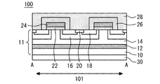
- FIG. 2 is a sectional view taken along the line AA of FIG.
- FIG. 3 is a cross-sectional view taken along the line BB of FIG.
- the semiconductor device 100 includes a semiconductor layer 11, a plurality of gate electrodes 24 provided on the upper surface of the semiconductor layer 11, a source electrode 28 provided on the upper surface of the semiconductor layer 11, and a surface opposite to the upper surface of the semiconductor layer 11.
- the drain electrode 30 provided in the above is provided.
- the semiconductor layer 11 has an active region 101 on which a MOSFET is formed and a terminal region 102 surrounding the active region 101 in a plan view.
- the semiconductor layer 11 is formed of silicon carbide.
- the semiconductor layer 11 has a substrate 10 containing n-type impurities and formed of SiC.
- the first semiconductor layer 12 is provided on the upper surface of the substrate 10.
- the first semiconductor layer 12 is an epitaxial growth layer containing n + type impurities.
- the first semiconductor layer 12 has a higher concentration than the substrate 10.
- the impurity concentration of the first semiconductor layer 12 is, for example, 4 ⁇ 10 18 cm -3 or more, and the thickness is 4 ⁇ m or more.
- the first semiconductor layer 12 has a function as a buffer layer.
- a second semiconductor layer 14 having a lower impurity concentration than the first semiconductor layer 12 is provided on the upper surface of the first semiconductor layer 12.
- the second semiconductor layer 14 is an epitaxial growth layer containing n-type impurities.
- a p-type well region 16 is provided on the upper surface side of the second semiconductor layer 14.
- the impurity concentration of the well region 16 is, for example, 1 ⁇ 10 18 cm -3 .
- a plurality of well regions 16 are selectively provided on the outermost surface of the second semiconductor layer 14.
- An n-type source region 18 is provided on the upper surface side of the well region 16.
- a p-type high concentration region 20 is provided between the adjacent source regions 18.
- the high concentration region 20 is also called a well contact region.
- the impurity concentration in the high concentration region 20 is, for example, 1 ⁇ 10 20 cm -3 .
- the well region 16 is provided on the upper surface side of the second semiconductor layer 14.
- a high concentration region 20 which is p-type and has a higher impurity concentration than the well region 16 is provided on the upper surface side of the well region 16.
- the high-concentration region 20 of the active region 101 and the high-concentration region 20 of the terminal region 102 are the same layer.
- the high concentration region 20 is formed simultaneously in the active region 101 and the terminal region 102.
- a withstand voltage holding region 32 is provided on the upper surface side of the second semiconductor layer 14 in the terminal region 102.
- the impurity concentration of the pressure resistance holding region 32 is, for example, 1 ⁇ 10 18 cm -3 .
- the high concentration region 20 has a higher impurity concentration than the pressure resistance holding region 32.
- the pressure resistance holding region 32 is provided on the outer periphery of the well region 16 in the terminal region 102. The arrangement of the withstand voltage holding region 32 and the impurity concentration are changed depending on the required withstand voltage class.
- a gate insulating film 22 is provided on the upper surface of the second semiconductor layer 14.
- the gate insulating film 22 is provided from the upper surface of the portion of the second semiconductor layer 14 sandwiched between the well regions 16 to the upper surface of the edge portion of the source region 18 through the upper surface of the well region 16.
- a gate electrode 24 is provided on the gate insulating film 22.
- the gate electrode 24 is provided directly above the portion of the second semiconductor layer 14, sandwiched between the well regions 16, the well region 16, and the source region 18.
- the gate insulating film 22 and the gate electrode 24 are covered with the interlayer insulating film 26.
- the interlayer insulating film 26 is covered with the source electrode 28.
- the source electrode 28 is in contact with and electrically connected to the portion of the source region 18 that is not covered with the interlayer insulating film 26 and the high concentration region 20.
- the gate electrode 24 is provided directly above the high concentration region 20 via the insulating film.
- one of the plurality of gate electrodes 24 is provided in the portion of the second semiconductor layer 14 sandwiched between the well region 16 and the withstand voltage holding region 32, directly above the well region 16 and the high concentration region 20. Be done.
- the source electrode 28 is extended to the terminal region 102. In the terminal region 102, the source electrode 28 is in contact with the portion of the high concentration region 20 that is not covered with the interlayer insulating film 26 and is electrically connected. The source electrode 28 is electrically connected to the high concentration region 20 by passing between the gate electrodes 24 provided above the termination region 102 and adjacent to each other.
- the semiconductor device 100 When the main current is energized in the semiconductor device 100, a current flows from the drain electrode 30 toward the source electrode 28. At this time, the semiconductor device 100 operates as a MOSFET. Further, when the reverse current is energized, a current flows from the source electrode 28 toward the drain electrode 30. At this time, the semiconductor device 100 operates as a PN diode.
- the PN diode that parasitizes inside the semiconductor device 100 is also called a body diode.
- BPD Basal Plane Dislocation
- the p-type high concentration region 20 is provided in the terminal region 102.
- a region having a high hole density that causes expansion of crystal defects can be formed in the terminal region 102, and a hole current can be easily passed through the terminal region 102. Therefore, it is possible to suppress the expansion of crystal defects to the active region 101 and suppress the deterioration of the electrical characteristics of the semiconductor device 100.
- the high concentration region 20 comes into contact with the source electrode 28.
- a PN diode different from the active region 101 can be formed in the terminal region 102, and the current path from the source electrode 28 can be concentrated in the terminal region 102. Therefore, the region where the Hall current flows can be further limited.
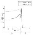
- FIG. 4 is a diagram illustrating the relationship between the first semiconductor layer 12 and the hole density.
- FIG. 4 shows a simulation result of the hole density around the boundary between the active region 101 and the terminal region 102 when a reverse current is passed through the semiconductor device 100.
- the region where X is positive is the terminal region 102, and the region where X is negative is the active region 101.
- the hole density indicates the hole density in the vicinity of the interface with the first semiconductor layer 12 in the substrate 10.
- the solid line in FIG. 4 shows the results when the impurity concentration of the first semiconductor layer 12 is 4 ⁇ 10 18 cm -3 and the thickness is 4 ⁇ m.
- the broken line in FIG. 4 shows the result when the impurity concentration of the first semiconductor layer 12 is 1 ⁇ 10 18 cm -3 and the thickness is 1 ⁇ m.
- the impurity concentration of the first semiconductor layer 12 is 4 ⁇ 10 18 cm -3 and the thickness is 4 ⁇ m
- the impurity concentration is 1 ⁇ 10 18 cm -3 and the thickness is 1 ⁇ m.
- the hole density in the active region 101 can be reduced as compared to the case.
- the first semiconductor layer 12 has a function of damming the Hall current flowing with the current during operation of the PN diode in the active region 101. Therefore, the hole density of the active region 101 can be reduced by the first semiconductor layer 12.
- the hole density of the terminal region 102 is about 1.5 times or more the hole density of the active region 101. At this time, in particular, the expansion of crystal defects to the active region 101 can be sufficiently suppressed, and the deterioration of the electrical characteristics of the semiconductor device 100 can be suppressed.
- the gate electrode 24 is also provided in the terminal region 102.
- the potential of the terminal region 102 can be stabilized.
- the potential around the well region 16 can be stabilized.
- the characteristics of the PN diode in the terminal region 102 can be stabilized, and the hole density can be stably controlled. Therefore, deterioration of the electrical characteristics of the semiconductor device 100 can be suppressed.
- the structure of the semiconductor device 100 is not limited to that described above.
- the semiconductor device 100 may be a MOSFET having a parasitic diode.
- concentration of each layer is an example. Further, if there is no problem in the characteristics of the PN diode in the terminal region 102, the gate electrode 24 may not be provided in the terminal region 102.
- FIG. 5 is a plan view of the semiconductor device 200 according to the second embodiment.
- the position where the high concentration region 20 is formed is different from that of the semiconductor device 100.
- Other structures are the same as those of the semiconductor device 100.
- the high-concentration region 20 in the terminal region 102 of the semiconductor device 200 is formed only on the side along the ⁇ 1-100> direction among the four sides of the terminal region 102 surrounding the active region 101 in a plan view.
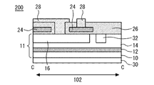
- FIG. 6 is a sectional view taken along the line CC of FIG.
- a high concentration region 20 which is a p + type impurity injection region is not formed on the side of the terminal region 102 along the ⁇ 11-20> direction.
- Such a high density region 20 can be formed by using a photolithography technique.
- the high-concentration region 20 is a p-type impurity in the semiconductor layer 11 using a resist mask that closes on the side along the ⁇ 11-20> direction and opens on the side along the ⁇ 1-100> direction.
- the growth direction of the defect is the ⁇ 1-100> direction shown in FIG. Therefore, when the high-concentration region 20 is formed on two sides of the terminal region 102 parallel to the ⁇ 11-20> direction, the defect may expand to the active region 101 starting from the BPD generated in the terminal region 102. be.
- the high concentration region 20 is not formed on the two sides parallel to the ⁇ 11-20> direction. Therefore, the region that is the starting point of the expansion of the crystal defect can be limited. Therefore, it is possible to suppress the expansion of crystal defects toward the central portion of the active region 101, and further suppress the deterioration of the electrical characteristics of the semiconductor device 200.
Landscapes
- Insulated Gate Type Field-Effect Transistor (AREA)
- Electrodes Of Semiconductors (AREA)
Abstract
Description
図1は、実施の形態1に係る半導体装置100の平面図である。以下ではn型が第1導電型であり、p型が第2導電型である。これに限らず、n型が第2導電型であり、p型が第1導電型であっても良い。また、活性領域とは半導体装置の主電流が流れる領域を示す。また、終端領域は活性領域の周辺に設けられる領域を示す。なお、図1では半導体装置100の構造を説明するため、電極、絶縁膜の一部が省略されている。
図5は、実施の形態2に係る半導体装置200の平面図である。半導体装置200では、高濃度領域20が形成される位置が半導体装置100と異なる。他の構造は半導体装置100と同様である。半導体装置200の終端領域102における高濃度領域20は、平面視で活性領域101を囲む終端領域102の4辺のうち、<1-100>方向に沿った辺にのみ形成される。
Claims (5)
- MOSFETが形成された活性領域と、平面視で前記活性領域を囲む終端領域と、を有する半導体層と、
前記半導体層の上面に設けられたゲート電極と、
前記半導体層の上面に設けられたソース電極と、
前記半導体層の上面と反対側の面に設けられたドレイン電極と、
を備え、
前記半導体層は、
第1導電型の第1半導体層と、
前記第1半導体層の上面に設けられ、前記第1導電型であり、前記第1半導体層よりも不純物濃度が低い第2半導体層と、
前記活性領域で前記第2半導体層の上面側に設けられ、第2導電型であるウェル領域と、
前記ウェル領域の上面側に設けられ、前記第1導電型であるソース領域と、
前記終端領域で前記第2半導体層の上面側に設けられ、前記第2導電型であり、前記ウェル領域よりも不純物濃度が高い高濃度領域と、
を備え、
前記ゲート電極は、前記ウェル領域の直上に設けられ、
前記ソース電極は、前記ソース領域および前記高濃度領域と電気的に接続され、
前記第1半導体層の不純物濃度は4×1018cm-3以上であり、厚さは4μm以上であることを特徴とする半導体装置。 - 前記ゲート電極を複数備え、
前記複数のゲート電極のうち前記終端領域の上に設けられ互いに隣接するゲート電極の間を通り、前記ソース電極は前記高濃度領域と電気的に接続されることを特徴とする請求項1に記載の半導体装置。 - 前記終端領域で前記第2半導体層の上面側に設けられた耐圧保持領域を備え、
前記高濃度領域は、前記耐圧保持領域よりも不純物濃度が高いことを特徴とする請求項1または2に記載の半導体装置。 - 前記半導体層は、炭化ケイ素から形成されることを特徴とする請求項1から3の何れか1項に記載の半導体装置。
- 前記高濃度領域は、平面視で前記活性領域を囲む前記終端領域の4辺のうち、<1-100>方向に沿った辺にのみ形成されることを特徴とする請求項1から4の何れか1項に記載の半導体装置。
Priority Applications (5)
| Application Number | Priority Date | Filing Date | Title |
|---|---|---|---|
| DE112020007709.8T DE112020007709T5 (de) | 2020-10-22 | 2020-10-22 | Halbleitervorrichtung |
| PCT/JP2020/039707 WO2022085151A1 (ja) | 2020-10-22 | 2020-10-22 | 半導体装置 |
| JP2022556327A JP7509225B2 (ja) | 2020-10-22 | 2020-10-22 | 半導体装置 |
| US18/000,232 US12501651B2 (en) | 2020-10-22 | 2020-10-22 | Semiconductor device |
| CN202080106313.9A CN116325170B (zh) | 2020-10-22 | 2020-10-22 | 半导体装置 |
Applications Claiming Priority (1)
| Application Number | Priority Date | Filing Date | Title |
|---|---|---|---|
| PCT/JP2020/039707 WO2022085151A1 (ja) | 2020-10-22 | 2020-10-22 | 半導体装置 |
Publications (1)
| Publication Number | Publication Date |
|---|---|
| WO2022085151A1 true WO2022085151A1 (ja) | 2022-04-28 |
Family
ID=81289771
Family Applications (1)
| Application Number | Title | Priority Date | Filing Date |
|---|---|---|---|
| PCT/JP2020/039707 Ceased WO2022085151A1 (ja) | 2020-10-22 | 2020-10-22 | 半導体装置 |
Country Status (5)
| Country | Link |
|---|---|
| US (1) | US12501651B2 (ja) |
| JP (1) | JP7509225B2 (ja) |
| CN (1) | CN116325170B (ja) |
| DE (1) | DE112020007709T5 (ja) |
| WO (1) | WO2022085151A1 (ja) |
Citations (4)
| Publication number | Priority date | Publication date | Assignee | Title |
|---|---|---|---|---|
| JP2015056644A (ja) * | 2013-09-13 | 2015-03-23 | 富士電機株式会社 | 炭化珪素半導体装置および炭化珪素半導体装置の製造方法 |
| JP2017112171A (ja) * | 2015-12-15 | 2017-06-22 | 株式会社日立製作所 | 半導体装置、パワーモジュール、電力変換装置、自動車および鉄道車両 |
| JP2020141130A (ja) * | 2019-02-27 | 2020-09-03 | 株式会社デンソー | 炭化珪素半導体装置およびその製造方法 |
| WO2020208761A1 (ja) * | 2019-04-11 | 2020-10-15 | 三菱電機株式会社 | 半導体装置および電力変換装置 |
Family Cites Families (9)
| Publication number | Priority date | Publication date | Assignee | Title |
|---|---|---|---|---|
| JP4185215B2 (ja) | 1999-05-07 | 2008-11-26 | 弘之 松波 | SiCウエハ、SiC半導体デバイス、および、SiCウエハの製造方法 |
| JP4224253B2 (ja) | 2002-04-24 | 2009-02-12 | パナソニック株式会社 | 半導体装置及びその製造方法 |
| JP6250938B2 (ja) * | 2013-03-05 | 2017-12-20 | 新日本無線株式会社 | 半導体装置及びその製造方法 |
| JP6617292B2 (ja) * | 2014-05-23 | 2019-12-11 | パナソニックIpマネジメント株式会社 | 炭化珪素半導体装置 |
| DE112014006752B4 (de) * | 2014-06-17 | 2025-04-17 | Hitachi, Ltd. | Halbleitervorrichtung, Leistungsmodul, Leistungsumsetzungsvorrichtung, Eisenbahnfahrzeug und Verfahren zum Herstellen der Halbleitervorrichtung |
| JP2018029104A (ja) * | 2016-08-16 | 2018-02-22 | 国立研究開発法人産業技術総合研究所 | 半導体装置およびその製造方法 |
| JP6932998B2 (ja) | 2017-05-25 | 2021-09-08 | 富士電機株式会社 | 炭化ケイ素mosfet及びその製造方法 |
| US11489069B2 (en) * | 2017-12-21 | 2022-11-01 | Wolfspeed, Inc. | Vertical semiconductor device with improved ruggedness |
| JP7275573B2 (ja) | 2018-12-27 | 2023-05-18 | 富士電機株式会社 | 炭化珪素半導体装置および炭化珪素半導体装置の製造方法 |
-
2020
- 2020-10-22 CN CN202080106313.9A patent/CN116325170B/zh active Active
- 2020-10-22 DE DE112020007709.8T patent/DE112020007709T5/de active Pending
- 2020-10-22 US US18/000,232 patent/US12501651B2/en active Active
- 2020-10-22 JP JP2022556327A patent/JP7509225B2/ja active Active
- 2020-10-22 WO PCT/JP2020/039707 patent/WO2022085151A1/ja not_active Ceased
Patent Citations (4)
| Publication number | Priority date | Publication date | Assignee | Title |
|---|---|---|---|---|
| JP2015056644A (ja) * | 2013-09-13 | 2015-03-23 | 富士電機株式会社 | 炭化珪素半導体装置および炭化珪素半導体装置の製造方法 |
| JP2017112171A (ja) * | 2015-12-15 | 2017-06-22 | 株式会社日立製作所 | 半導体装置、パワーモジュール、電力変換装置、自動車および鉄道車両 |
| JP2020141130A (ja) * | 2019-02-27 | 2020-09-03 | 株式会社デンソー | 炭化珪素半導体装置およびその製造方法 |
| WO2020208761A1 (ja) * | 2019-04-11 | 2020-10-15 | 三菱電機株式会社 | 半導体装置および電力変換装置 |
Also Published As
| Publication number | Publication date |
|---|---|
| JPWO2022085151A1 (ja) | 2022-04-28 |
| CN116325170B (zh) | 2025-09-02 |
| CN116325170A (zh) | 2023-06-23 |
| DE112020007709T5 (de) | 2023-08-03 |
| US12501651B2 (en) | 2025-12-16 |
| US20230207681A1 (en) | 2023-06-29 |
| JP7509225B2 (ja) | 2024-07-02 |
Similar Documents
| Publication | Publication Date | Title |
|---|---|---|
| US20180277437A1 (en) | Semiconductor device | |
| JP5321377B2 (ja) | 電力用半導体装置 | |
| JP6560444B2 (ja) | 半導体装置 | |
| US10361267B2 (en) | Semiconductor device | |
| CN113178479A (zh) | 半导体装置 | |
| US11264451B2 (en) | Semiconductor device exhibiting soft recovery characteristics | |
| US11710734B2 (en) | Cascode-connected JFET-MOSFET semiconductor device | |
| CN111295763B (zh) | 宽带隙半导体装置 | |
| US11309415B2 (en) | Wide gap semiconductor device | |
| WO2012124191A1 (ja) | 半導体装置 | |
| JPH06224426A (ja) | 半導体装置 | |
| US10770579B2 (en) | SiC-MOSFET and method of manufacturing the same | |
| US20100084684A1 (en) | Insulated gate bipolar transistor | |
| JP7113386B2 (ja) | 半導体装置 | |
| JP2015159235A (ja) | 半導体装置 | |
| US20220293783A1 (en) | SiC-MOSFET | |
| WO2022085151A1 (ja) | 半導体装置 | |
| JP2019160877A (ja) | 半導体装置 | |
| JP7167881B2 (ja) | 半導体装置 | |
| US20190305126A1 (en) | Semiconductor device | |
| KR20070048753A (ko) | 서지 보호용 반도체 장치 | |
| JP7628874B2 (ja) | 半導体装置及びその製造方法 | |
| JP7334638B2 (ja) | 半導体装置 | |
| JP5082260B2 (ja) | 炭化珪素半導体装置 | |
| JP2025035323A (ja) | 半導体装置 |
Legal Events
| Date | Code | Title | Description |
|---|---|---|---|
| 121 | Ep: the epo has been informed by wipo that ep was designated in this application |
Ref document number: 20958703 Country of ref document: EP Kind code of ref document: A1 |
|
| ENP | Entry into the national phase |
Ref document number: 2022556327 Country of ref document: JP Kind code of ref document: A |
|
| 122 | Ep: pct application non-entry in european phase |
Ref document number: 20958703 Country of ref document: EP Kind code of ref document: A1 |
|
| WWG | Wipo information: grant in national office |
Ref document number: 202080106313.9 Country of ref document: CN |
|
| WWG | Wipo information: grant in national office |
Ref document number: 18000232 Country of ref document: US |