WO2022075263A1 - Récipient comprenant un module rfid - Google Patents
Récipient comprenant un module rfid Download PDFInfo
- Publication number
- WO2022075263A1 WO2022075263A1 PCT/JP2021/036638 JP2021036638W WO2022075263A1 WO 2022075263 A1 WO2022075263 A1 WO 2022075263A1 JP 2021036638 W JP2021036638 W JP 2021036638W WO 2022075263 A1 WO2022075263 A1 WO 2022075263A1
- Authority
- WO
- WIPO (PCT)
- Prior art keywords
- container
- rfid module
- flap
- metal film
- slit
- Prior art date
Links
Images


Classifications
-
- G—PHYSICS
- G06—COMPUTING; CALCULATING OR COUNTING
- G06K—GRAPHICAL DATA READING; PRESENTATION OF DATA; RECORD CARRIERS; HANDLING RECORD CARRIERS
- G06K19/00—Record carriers for use with machines and with at least a part designed to carry digital markings
- G06K19/06—Record carriers for use with machines and with at least a part designed to carry digital markings characterised by the kind of the digital marking, e.g. shape, nature, code
- G06K19/067—Record carriers with conductive marks, printed circuits or semiconductor circuit elements, e.g. credit or identity cards also with resonating or responding marks without active components
- G06K19/07—Record carriers with conductive marks, printed circuits or semiconductor circuit elements, e.g. credit or identity cards also with resonating or responding marks without active components with integrated circuit chips
- G06K19/077—Constructional details, e.g. mounting of circuits in the carrier
- G06K19/07749—Constructional details, e.g. mounting of circuits in the carrier the record carrier being capable of non-contact communication, e.g. constructional details of the antenna of a non-contact smart card
- G06K19/07798—Constructional details, e.g. mounting of circuits in the carrier the record carrier being capable of non-contact communication, e.g. constructional details of the antenna of a non-contact smart card part of the antenna or the integrated circuit being adapted for rupturing or breaking, e.g. record carriers functioning as sealing devices for detecting not-authenticated opening of containers
-
- B—PERFORMING OPERATIONS; TRANSPORTING
- B65—CONVEYING; PACKING; STORING; HANDLING THIN OR FILAMENTARY MATERIAL
- B65D—CONTAINERS FOR STORAGE OR TRANSPORT OF ARTICLES OR MATERIALS, e.g. BAGS, BARRELS, BOTTLES, BOXES, CANS, CARTONS, CRATES, DRUMS, JARS, TANKS, HOPPERS, FORWARDING CONTAINERS; ACCESSORIES, CLOSURES, OR FITTINGS THEREFOR; PACKAGING ELEMENTS; PACKAGES
- B65D25/00—Details of other kinds or types of rigid or semi-rigid containers
- B65D25/20—External fittings
-
- B—PERFORMING OPERATIONS; TRANSPORTING
- B65—CONVEYING; PACKING; STORING; HANDLING THIN OR FILAMENTARY MATERIAL
- B65D—CONTAINERS FOR STORAGE OR TRANSPORT OF ARTICLES OR MATERIALS, e.g. BAGS, BARRELS, BOTTLES, BOXES, CANS, CARTONS, CRATES, DRUMS, JARS, TANKS, HOPPERS, FORWARDING CONTAINERS; ACCESSORIES, CLOSURES, OR FITTINGS THEREFOR; PACKAGING ELEMENTS; PACKAGES
- B65D5/00—Rigid or semi-rigid containers of polygonal cross-section, e.g. boxes, cartons or trays, formed by folding or erecting one or more blanks made of paper
- B65D5/42—Details of containers or of foldable or erectable container blanks
-
- G—PHYSICS
- G06—COMPUTING; CALCULATING OR COUNTING
- G06K—GRAPHICAL DATA READING; PRESENTATION OF DATA; RECORD CARRIERS; HANDLING RECORD CARRIERS
- G06K19/00—Record carriers for use with machines and with at least a part designed to carry digital markings
- G06K19/06—Record carriers for use with machines and with at least a part designed to carry digital markings characterised by the kind of the digital marking, e.g. shape, nature, code
- G06K19/067—Record carriers with conductive marks, printed circuits or semiconductor circuit elements, e.g. credit or identity cards also with resonating or responding marks without active components
- G06K19/07—Record carriers with conductive marks, printed circuits or semiconductor circuit elements, e.g. credit or identity cards also with resonating or responding marks without active components with integrated circuit chips
- G06K19/0701—Record carriers with conductive marks, printed circuits or semiconductor circuit elements, e.g. credit or identity cards also with resonating or responding marks without active components with integrated circuit chips at least one of the integrated circuit chips comprising an arrangement for power management
- G06K19/0707—Record carriers with conductive marks, printed circuits or semiconductor circuit elements, e.g. credit or identity cards also with resonating or responding marks without active components with integrated circuit chips at least one of the integrated circuit chips comprising an arrangement for power management the arrangement being capable of collecting energy from external energy sources, e.g. thermocouples, vibration, electromagnetic radiation
- G06K19/0708—Record carriers with conductive marks, printed circuits or semiconductor circuit elements, e.g. credit or identity cards also with resonating or responding marks without active components with integrated circuit chips at least one of the integrated circuit chips comprising an arrangement for power management the arrangement being capable of collecting energy from external energy sources, e.g. thermocouples, vibration, electromagnetic radiation the source being electromagnetic or magnetic
-
- G—PHYSICS
- G06—COMPUTING; CALCULATING OR COUNTING
- G06K—GRAPHICAL DATA READING; PRESENTATION OF DATA; RECORD CARRIERS; HANDLING RECORD CARRIERS
- G06K19/00—Record carriers for use with machines and with at least a part designed to carry digital markings
- G06K19/06—Record carriers for use with machines and with at least a part designed to carry digital markings characterised by the kind of the digital marking, e.g. shape, nature, code
- G06K19/067—Record carriers with conductive marks, printed circuits or semiconductor circuit elements, e.g. credit or identity cards also with resonating or responding marks without active components
- G06K19/07—Record carriers with conductive marks, printed circuits or semiconductor circuit elements, e.g. credit or identity cards also with resonating or responding marks without active components with integrated circuit chips
- G06K19/077—Constructional details, e.g. mounting of circuits in the carrier
- G06K19/07749—Constructional details, e.g. mounting of circuits in the carrier the record carrier being capable of non-contact communication, e.g. constructional details of the antenna of a non-contact smart card
- G06K19/07758—Constructional details, e.g. mounting of circuits in the carrier the record carrier being capable of non-contact communication, e.g. constructional details of the antenna of a non-contact smart card arrangements for adhering the record carrier to further objects or living beings, functioning as an identification tag
-
- G—PHYSICS
- G06—COMPUTING; CALCULATING OR COUNTING
- G06K—GRAPHICAL DATA READING; PRESENTATION OF DATA; RECORD CARRIERS; HANDLING RECORD CARRIERS
- G06K19/00—Record carriers for use with machines and with at least a part designed to carry digital markings
- G06K19/06—Record carriers for use with machines and with at least a part designed to carry digital markings characterised by the kind of the digital marking, e.g. shape, nature, code
- G06K19/067—Record carriers with conductive marks, printed circuits or semiconductor circuit elements, e.g. credit or identity cards also with resonating or responding marks without active components
- G06K19/07—Record carriers with conductive marks, printed circuits or semiconductor circuit elements, e.g. credit or identity cards also with resonating or responding marks without active components with integrated circuit chips
- G06K19/077—Constructional details, e.g. mounting of circuits in the carrier
- G06K19/07749—Constructional details, e.g. mounting of circuits in the carrier the record carrier being capable of non-contact communication, e.g. constructional details of the antenna of a non-contact smart card
- G06K19/07771—Constructional details, e.g. mounting of circuits in the carrier the record carrier being capable of non-contact communication, e.g. constructional details of the antenna of a non-contact smart card the record carrier comprising means for minimising adverse effects on the data communication capability of the record carrier, e.g. minimising Eddy currents induced in a proximate metal or otherwise electromagnetically interfering object
-
- H—ELECTRICITY
- H01—ELECTRIC ELEMENTS
- H01Q—ANTENNAS, i.e. RADIO AERIALS
- H01Q1/00—Details of, or arrangements associated with, antennas
- H01Q1/36—Structural form of radiating elements, e.g. cone, spiral, umbrella; Particular materials used therewith
- H01Q1/38—Structural form of radiating elements, e.g. cone, spiral, umbrella; Particular materials used therewith formed by a conductive layer on an insulating support
-
- H—ELECTRICITY
- H01—ELECTRIC ELEMENTS
- H01Q—ANTENNAS, i.e. RADIO AERIALS
- H01Q1/00—Details of, or arrangements associated with, antennas
- H01Q1/44—Details of, or arrangements associated with, antennas using equipment having another main function to serve additionally as an antenna, e.g. means for giving an antenna an aesthetic aspect
-
- H—ELECTRICITY
- H01—ELECTRIC ELEMENTS
- H01Q—ANTENNAS, i.e. RADIO AERIALS
- H01Q1/00—Details of, or arrangements associated with, antennas
- H01Q1/50—Structural association of antennas with earthing switches, lead-in devices or lightning protectors
-
- H—ELECTRICITY
- H01—ELECTRIC ELEMENTS
- H01Q—ANTENNAS, i.e. RADIO AERIALS
- H01Q19/00—Combinations of primary active antenna elements and units with secondary devices, e.g. with quasi-optical devices, for giving the antenna a desired directional characteristic
- H01Q19/02—Details
-
- H—ELECTRICITY
- H01—ELECTRIC ELEMENTS
- H01Q—ANTENNAS, i.e. RADIO AERIALS
- H01Q5/00—Arrangements for simultaneous operation of antennas on two or more different wavebands, e.g. dual-band or multi-band arrangements
- H01Q5/30—Arrangements for providing operation on different wavebands
- H01Q5/307—Individual or coupled radiating elements, each element being fed in an unspecified way
- H01Q5/314—Individual or coupled radiating elements, each element being fed in an unspecified way using frequency dependent circuits or components, e.g. trap circuits or capacitors
- H01Q5/335—Individual or coupled radiating elements, each element being fed in an unspecified way using frequency dependent circuits or components, e.g. trap circuits or capacitors at the feed, e.g. for impedance matching
-
- H—ELECTRICITY
- H01—ELECTRIC ELEMENTS
- H01Q—ANTENNAS, i.e. RADIO AERIALS
- H01Q9/00—Electrically-short antennas having dimensions not more than twice the operating wavelength and consisting of conductive active radiating elements
- H01Q9/04—Resonant antennas
- H01Q9/16—Resonant antennas with feed intermediate between the extremities of the antenna, e.g. centre-fed dipole
- H01Q9/28—Conical, cylindrical, cage, strip, gauze, or like elements having an extended radiating surface; Elements comprising two conical surfaces having collinear axes and adjacent apices and fed by two-conductor transmission lines
Definitions
- the present invention relates to a container equipped with an RFID module, particularly a container equipped with an RFID module using RFID (Radio Frequency Identification) technology for non-contact data communication by an induced electromagnetic field or radio waves.
- RFID Radio Frequency Identification
- RFID tags which are a wireless communication device
- RFIC Radio-Frequency Integrated Circuit
- metal materials such as antenna patterns are formed on insulating substrates such as paper materials and resin materials.
- a metal film is formed on the outer surface of the container, the RFID tag is affected and communication becomes impossible.
- Patent Document 1 proposes a configuration in which an RFID tag compatible with a metal formed in a part of the container is provided so as not to impair the design.
- the RFID tag disclosed in Patent Document 1 has an RFID chip and an antenna pattern, and a metal film cannot be formed on the container in these regions. Therefore, there is a demand for a container having an RFID module that suppresses a reduction in the degree of freedom in design.
- An object of the present invention is to provide a container having an RFID module in which a reduction in design is suppressed in a container on which a metal film is formed.
- the container according to one aspect of the present invention is a container provided with an RFID module, the insulating base material, a metal film formed on the first main surface of the base material, and the metal film as a first metal region and a first metal film. It is provided with a slit formed so as to separate from the two metal regions.
- the RFID module includes an RFIC element, a filter circuit for transmitting a current due to an electromagnetic wave having a unique resonance frequency which is a communication frequency to the RFIC element, and first and second electrodes connected to the filter circuit. The first electrode of the RFID module and the first metal region of the metal film are electrically connected, and the second electrode of the RFID module and the second metal region of the metal film are electrically connected.
- the present invention it is possible to provide a container having an RFID module in which a reduction in design is suppressed in a container on which a metal film is formed.
- FIG. 6a is a plan view of the conductor pattern formed on the upper surface of the substrate of the RFID module
- FIG. 6b is a plan view of the conductor pattern formed on the lower surface of the substrate.
- Explanatory drawing which shows the manufacturing process of the container of Embodiment 1.
- Development view of the container in the modified example of the first embodiment Development view of the container in the modified example of the first embodiment Development view of the container in the modified example of the first embodiment Development view of the container in the modified example of the first embodiment Development view of the container in the modified example of the first embodiment Development view of the container in the modified example of the first embodiment Development view of the container in the modified example of the first embodiment Development view of the container in the modified example of the first embodiment
- One aspect of the container according to the present invention is a container provided with an RFID module, which comprises an insulating base material, a metal film formed on the first main surface of the base material, and a metal film as a first metal region. It comprises a slit formed so as to separate from the second metal region.
- the RFID module includes an RFIC element, a filter circuit for transmitting a current due to an electromagnetic wave having a unique resonance frequency which is a communication frequency to the RFIC element, and first and second electrodes connected to the filter circuit.
- the first electrode of the RFID module and the first metal region of the metal film are electrically connected, and the second electrode of the RFID module and the second metal region of the metal film are electrically connected.
- the container of this embodiment uses the first metal region and the second metal region of the metal film formed on the first main surface of the base material of the container as an antenna, the container on which the metal film is formed has a design property.
- the RFID module can be attached to the container with less freedom.
- the metal film when the metal film is irradiated with an electromagnetic wave having a communication frequency, a current may flow in a direction intersecting the slit.
- the metal film functions as a dipole antenna, communication characteristics as a dipole antenna can be obtained.
- the length in the direction orthogonal to the slit of the metal film may have an electrical length of half the wavelength of the electromagnetic wave of the communication frequency. In this case, the maximum communication distance as a dipole antenna can be obtained.
- the slit may go around the side of the container. As a result, even if a plurality of containers are arranged in the same direction, the slits do not come into contact with each other, and the first metal region and the second metal region of the metal film of each container do not conduct with each other without passing through the RFID module. Therefore, it is possible to communicate with multiple containers at once.
- the first metal region and the second metal region may be line-symmetrical with respect to the slit.
- the base material has a flap continuous with the first surface for connecting the first surface and the second surface on which the metal film is formed by an adhesive layer, the metal film is also formed on the flap, and the slit is a flap. Also formed, the RFID module may be placed on the flap. As a result, in the container, the RFID module arranged on the flap continuous with the first surface is attached to the inner surface of the second surface, so that it does not appear on the outer surface of the container. Therefore, it is possible to prevent the design of the container from being reduced.
- One end of the slit may extend to the end of the flap.
- the first divided slit In the region on one side of the flap where the metal film of the flap is divided by the slit, the first divided slit forming a metal region discontinuous with the first metal region of the flap and the first metal region of the first surface, and the slit. It comprises a second metal region of the flap and a second split slit forming a discontinuous metal region with the second metal region of the first surface in the region on the other side of the flap into which the metal film of the flap is divided. You may. As a result, the ratio of the first metal region and the second metal region in the flap can be reduced, so that the variation in communication characteristics due to the variation in the attachment distance between the flap and the second surface can be reduced.
- the RFID module may be arranged on the second main surface opposite to the first main surface of the base material. As a result, the RFID module does not appear on the outer surface of the container, so that it is possible to prevent the design of the container from being reduced.
- the metal film may be formed on the entire surface of the first main surface of the base material except for the slit.
- a design in which a metal film is formed on the entire surface of the first main surface of the container is also feasible.
- the flap has a non-metal region on which no metal film is formed on the first main surface of the flap, and even if the non-metal region of the flap and the second main surface of the second surface are bonded via the adhesive layer. good.
- the filter circuit may be an LC parallel resonant circuit. As a result, a current having a frequency matching the RFIC can be passed through the RFIC.
- the sheet resistance of the metal film may be 0.5 ⁇ / ⁇ or more. Even with this configuration, since the RFID module has a filter circuit, the eddy current generated in the metal film can be used to flow through the RFID.
- the thickness of the metal film may be 1 nm or more and 1 ⁇ m or less. Even with this configuration, since the RFID module has a filter circuit, the eddy current generated in the metal film can be used to flow through the RFID.
- the electrical length of the antenna pattern and the conductor pattern is longer than the physical length.
- the electrical length is a length considering the shortening or extension of the wavelength due to the relative permittivity and the parasitic reactance component.
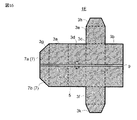
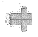
- FIG. 1 is an overall perspective view of a container 1 having an RFID module 5 according to the first embodiment of the present invention.
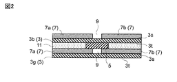
- FIG. 2 is a cross-sectional view taken along the line II-II in FIG. 1
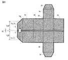
- FIG. 3 is a developed view of the container 1 in FIG.
- the container 1 of the first embodiment divides the base material 3, the RFID module 5 attached to the base material 3, the metal film 7 formed on the first main surface 3s of the base material 3, and the metal film 7.
- the slit 9 formed in the above manner is provided.
- the container 1 is formed into a three-dimensional shape by assembling a flat base material 3 as shown in FIG. 3, for example.
- the container 1 has a rectangular parallelepiped shape, for example, and the base material 3 is made of, for example, paper, resin, or plastic.
- the base material 3 includes a first surface 3a, a second surface 3b, a third surface 3c, a fourth surface 3d, a fifth surface 3e, a sixth surface 3f, and a first flap 3g, a second flap 3h, and a third flap. Equipped with 3k.
- the first surface 3a to the fourth surface 3d become a side surface when assembled
- the fifth surface 3e becomes an upper surface when assembled
- the sixth surface 3f becomes a lower surface when assembled.
- the first main surface 3s of the base material 3 is a surface to be the outer surface (front surface) of the container 1
- the second main surface 3t of the base material 3 is a surface to be the inner surface (back surface) of the container 1.
- the first main surface 3s of the first flap 3g is attached to the second main surface 3t of the second surface 3b via the adhesive layer 11 when assembled.
- the first main surface 3s of the second flap 3h is attached to the second main surface 3t of the first surface 3a via the adhesive layer 11 when assembled.
- the first main surface 3s of the third flap 3k is attached to the second main surface 3t of the first surface 3a via the adhesive layer 11 when assembled.
- the metal film 7 is formed on the entire surface of the first main surface 3s of the base material 3 except for the slit 9.
- the metal film 7 is made of a film body of a conductive material such as aluminum foil or copper foil, and is formed by, for example, attaching a metal sheet. By using a metal having a small resistance value such as aluminum or copper as the metal film 7, the communication distance can be increased.
- the thickness of the metal film 7 is, for example, larger than 5 ⁇ m and 40 ⁇ m or less.
- the metal film 7 is physically divided into two or more regions by the slit 9.
- the metal film 7 is divided into two regions, a first metal region 7a and a second metal region 7b, and the first metal region 7a and the second metal region 7b are electrically insulated by a slit 9. ing.
- the metal film 7 may not be formed on the entire surface of the base material 3, and may be partially formed on, for example, the first flap 3g and other surfaces.
- the metal film 7 has a first metal region 7a extending outward from the container 1 in a direction intersecting the slit 9, and outward of the container 1 in a direction intersecting the slit 9 and opposite to the first metal region 7a.
- the second metal region 7b extending toward it functions as a dipole type antenna.
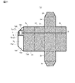
- the distance Lg1 from the slit 9 to one end of the first flap 3g in the direction orthogonal to the slit 9 and the distance Lg2 from the slit 9 to the other end of the first flap 3g in the direction orthogonal to the slit 9 are the same length. Is. Further, when the total length of the sum of the distance Lg1, the distance Lg2, and the width W of the slit 9 is the length of the high frequency half wavelength of the communication frequency, the communication distance is maximized.
- the length of the high frequency half wavelength of the communication frequency may be, for example, the length in the direction orthogonal to the position of the slit 9 to which the RFID module 5 is attached.
- the slit 9 is a groove that divides the metal film 7.
- the width W of the slit 9 is, for example, 0.5 mm to 3 mm.
- the slit 9 may be formed by forming a metal film 7 on the entire first main surface 3s of the base material 3 and then scraping the metal film 7, or two metal sheets may be formed with the width of the slit 9 open. It may be formed by attaching it to the first main surface 3S of the material 3. One end of the slit 9 extends to the end of the first flap 3g.
- the RFID module 5 of the first embodiment is a wireless communication device configured to perform wireless communication (transmission / reception) with a high frequency signal having a communication frequency (carrier frequency).
- the RFID module 5 is configured to perform wireless communication with, for example, a high frequency signal having a frequency for communication in the UHF band.
- the UHF band is a frequency band from 860 MHz to 960 MHz.
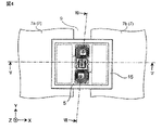
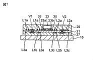
- FIG. 4 is a perspective plan view of the RFID module
- FIG. 5 is a cross-sectional view of arrow V in FIG.
- FIG. 6 shows a plan view of a conductor pattern formed on the substrate of the RFID module
- FIG. 6a is a plan view of the conductor pattern formed on the upper surface of the substrate of the RFID module
- FIG. 6b is a plan view of the conductor pattern formed on the lower surface of the substrate. It is a perspective plan view seen from the top of the conductor pattern.
- FIG. 7 is a cross-sectional view taken along the line VII in FIG.
- the XYZ coordinate system facilitates the understanding of the invention and does not limit the invention.
- the X-axis direction indicates the longitudinal direction of the RFID module 5
- the Y-axis direction indicates the depth (width) direction
- the Z-axis direction indicates the thickness direction.
- the X, Y, and Z directions are orthogonal to each other.
- the RFID module 5 is attached to the upper surfaces of the first metal region 7a and the second metal region 7b of the metal film 7 via an adhesive layer 11 such as double-sided tape or synthetic resin.
- the RFID module 5 includes a substrate 21 and an RFID 23 mounted on the substrate 21.
- the substrate 21 is a flexible substrate such as polyimide.
- a protective film 25 is formed on the upper surface of the substrate 21 on which the RFIC 23 is mounted.
- the protective film 25 is, for example, an elastomer such as polyurethane or a hot melt agent such as ethylene vinyl acetate (EVA).
- a protective film 27 is also attached to the lower surface of the substrate 21.
- the protective film 27 is, for example, a coverlay film such as a polyimide film (Kapton tape).
- a third electrode 33, a fourth electrode 35, a conductor pattern L1a of the main portion of the first inductance element L1 and a conductor pattern L2a of the main portion of the second inductance element L2 are formed on the upper surface of the substrate 21, a third electrode 33, a fourth electrode 35, a conductor pattern L1a of the main portion of the first inductance element L1 and a conductor pattern L2a of the main portion of the second inductance element L2 are formed.
- the third electrode 33 is connected to one end of the conductor pattern L1a
- the fourth electrode 35 is connected to one end of the conductor pattern L2a.
- These conductor patterns are, for example, a copper foil patterned by photolithography.
- the first electrode 29 and the second electrode 31 are capacitively coupled to the first metal region 7a and the second metal region 7b of the metal film 7, respectively. Further, on the lower surface of the substrate 21, a part of the conductor pattern L1b of the first inductance element L1 and the conductor patterns L3a, L3b (conductor pattern surrounded by the alternate long and short dash line) and L3c of the third inductance element L3 are formed. These conductor patterns are also, for example, a copper foil patterned by photolithography.
- One end of a part of the conductor pattern L1b of the first inductance element L1 and one end of the conductor pattern L3a of the third inductance element L3 are connected to the first electrode 29.
- one end of the conductor pattern L2b of the second inductance element L2 and one end of the conductor pattern L3c of the third inductance element L3 are connected to the second electrode 31.
- a conductor pattern L3b is connected between the other end of the conductor pattern L3a of the third inductance element L3 and the other end of the conductor pattern L3c.
- the other end of the conductor pattern L1b of the first inductance element L1 and the other end of the conductor pattern L1a of the first inductance element L1 are connected via the via conductor V1.
- the other end of the conductor pattern L2b of the second inductance element L2 and the other end of the conductor pattern L2a of the second inductance element L2 are connected via the via conductor V2.
- the RFIC 23 is mounted on the third electrode 33 and the fourth electrode 35 formed on the upper surface of the substrate 21. That is, the terminal 23a of the RFIC 23 is connected to the third electrode 33, and the terminal 23b of the RFIC 23 is connected to the fourth electrode 35.
- the conductor patterns L3a of the first inductance element L1 and the third inductance element L3 are formed in different layers of the substrate 21, and are arranged so that their coil openings overlap each other.
- the conductor patterns L3c of the second inductance element L2 and the third inductance element L3 are formed in different layers of the substrate 21, and their coil openings are arranged so as to overlap each other.
- the RFIC 23 is positioned on the surface of the substrate 21 between the conductor pattern L3c of the second inductance element L2 and the third inductance element L3 and the conductor pattern L3a of the first inductance element L1 and the third inductance element L3. do.
- a first current path CP1 passing through the upper surface and the lower surface of the substrate 21 and a second current path CP2 passing through the lower surface of the substrate 21 are formed.
- the first current path CP1 reaches the second electrode 31 from the first electrode 29 through the branch point N1, the conductor pattern L1b, the conductor pattern L1a, RFIC23, the conductor pattern L2a, the conductor pattern L2b, and the branch point N2.
- the second current path CP2 reaches the second electrode 31 from the first electrode 29 through the branch point N1, the conductor pattern L3a, the conductor pattern L3b, the conductor pattern L3c, and the branch point N2.
- first inductance element L1 composed of a conductor pattern L1b connected via a conductor pattern L1a and a via conductor V1, and a conductor pattern L2b connected via a conductor pattern L2a and a via conductor V2.
- the winding directions of the current flowing through the second inductance element L2 are opposite to each other, and the magnetic field generated by the first inductance element L1 and the magnetic field generated by the second inductance element L2 cancel each other out.
- the first current path CP1 and the second current path CP2 are formed in parallel with each other between the first electrode 29 and the second electrode 31, respectively.
- FIG. 8 is a circuit diagram of the RFID module 5.
- the first current path CP1 is a part of the parallel resonant circuit RC1 which is an LC parallel resonant circuit, and matches the radio wave of the communication frequency. Therefore, the radio wave of the communication frequency is transmitted to the metal film 7. Is received, a current flows through the RFIC 23.
- the RFID module 5 is formed with a parallel resonant circuit RC1.
- the parallel resonant circuit RC1 is a loop circuit composed of a first inductance element L1, an RFIC23, a second inductance element L2, and a third inductance element L3.
- the capacitance C1 is composed of a first metal region 7a, a first electrode 29, an adhesive layer 11, and a protective film 27.
- the capacitance C2 is composed of a second metal region 7b, a second electrode 31, an adhesive layer 11, and a protective film 27.
- the fourth inductance element L4 is an inductance component of the first metal region 7a of the metal film 7
- the fifth inductance element L5 is an inductance component of the second metal region 7b of the metal film 7.
- the parallel resonance circuit RC1 is designed to perform LC parallel resonance by impedance matching with radio waves at the communication frequency. As a result, the RFID module is matched with the RFID in the communication frequency, and the communication distance of the RFID module 5 in the communication frequency can be secured.
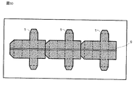
- a slit 9 is formed in the central portion in the longitudinal direction of the first surface 3a, the second surface 3b, the third surface 3c, and the fourth surface 3d, which are the side surfaces, respectively. Even if a plurality of containers 1 are arranged side by side as shown, the slits 9 of the respective containers 1 overlap each other. Therefore, in the first metal region 7a and the second metal region 7b of the metal film 7 of each container 1, the insulated state is maintained unless the RFID module 5 is passed through, so that communication with a plurality of containers 1 can be performed. Can be done at once.
- the container 1 of the first embodiment has a metal film 7 formed on the front surface of the first main surface 3s of the unfolded container 1 before assembly, with respect to a plurality of containers 1 before assembly.
- the slit 9 can be formed at once.
- the insulating base material 3, the metal film 7 formed on the first main surface 3s of the base material 3, and the metal film 7 are the first metal regions 7a and the first.
- An RFID module 5 including first and second electrodes 29 and 31 connected to RC1 is provided, and the first electrode 29 of the RFID module 5 and the first metal region 7a of the metal film 7 are electrically connected. , The second electrode 31 of the RFID module 5 and the second metal region 7b of the metal film 7 are electrically connected.
- the RFID module 5 is arranged across the slit 9 that divides the metal film 7 formed on the base material 3 of the container 1 into the first metal region 7a and the second metal region 7b, the first and second metals
- the regions 7a and 7b can be used as antenna electrodes, respectively, and a current can be passed through the RFID 23 by series resonance. Therefore, even if the container 1 is formed with the metal film 7, wireless communication is possible, and it is possible to provide the container 1 having the RFID module 5 in which the reduction in design is suppressed.
- the container 1 of the embodiment can be provided at a lower cost than the container to which the conventional metal-compatible RFID module is attached.
- the conventional flag type RFID module pops out of the container and breaks, the communication characteristics will deteriorate.
- the RFID module since the RFID module must be ejected from the container, the degree of freedom in design is reduced, but in the case of the container 1 of the embodiment, the RFID module does not have to be ejected from the container, so that the degree of freedom in design is reduced. Can be suppressed.
- the metal film 7 When the metal film 7 is irradiated with an electromagnetic wave having a communication frequency, a current flows in the direction intersecting the slit 9. As described above, since the metal film 7 functions as a dipole antenna, it is possible to obtain communication characteristics as a dipole antenna.
- the length of the metal film 7 in the direction orthogonal to the slit 9 has an electrical length of half the wavelength of the electromagnetic wave of the communication frequency. As a result, the maximum communication distance of the metal film 7 as a dipole antenna can be obtained.
- the slit 9 orbits the first surface 3a to the fourth surface 3d, which are the side surfaces of the container 1. As a result, even if a plurality of containers 1 are arranged in the same direction, the slits 9 come into contact with each other, and the first metal region 7a and the second metal region 7b of the metal film 7 of each container 1 pass through the RFID module 5. Since it does not conduct without conducting, it is possible to communicate with a plurality of containers 1 at one time.
- the first metal region 7a and the second metal region 7b may be line-symmetrical with respect to the slit 9.
- the slits 9 come into contact with each other, and the first metal region 7a and the second metal region of the metal film 7 of each container 1 come into contact with each other.
- 7b and 7b do not conduct without passing through the RFID module 5. Therefore, the operator can reduce the attention to the orientation of the container 1.
- the base material 3 has a first flap 3g continuous with the first surface 3a for connecting the first surface 3a and the second surface 3b on which the metal film 7 is formed by the adhesive layer 11, and the metal film 7 Is also formed in the first flap 3g, the slit 9 is also formed in the first flap 3g, and the RFID module 5 may be arranged in the first flap 3g.
- the RFID module 5 arranged on the first flap 3g continuous with the first surface 3a is attached to the inner surface of the second surface 3b, so that it does not appear on the outer surface of the container 1. Therefore, it is possible to prevent the design of the container 1 from being reduced.
- the metal film 7 is formed on the entire surface of the first main surface 3s of the base material 3 except for the slit 9. As described above, a design in which the metal film 7 is formed on the entire surface of the first main surface 3s of the container 1 can be realized.
- FIG. 11 is a developed view of the container 1A in the first modification of the first embodiment.
- the container 1A in the first modification of the first embodiment has a structure in which the slit 9 of the container 1 of the first embodiment is shifted downward.
- Other configurations are substantially the same as the container 1 of the first embodiment.
- the container 1A in the first modification has a short electrical length orthogonal to the slit 9 in the second metal region 7b, the communication characteristics are lower than those of the container 1 of the first embodiment, but communication is possible. Further, as shown in FIG. 12, even if a plurality of containers 1 are brought into contact with each other and arranged, the first metal region 7a and the second metal region 7b are RFID by aligning the orientations so that the slits 9 are in contact with each other. Since the conduction state does not occur without passing through the module 5, it is possible to perform wireless communication collectively. Further, by inserting the slit at a position where the content of the container 1A does not cover the slit 9, deterioration of the reading distance is reduced even if the content is a metal object or water.
- FIG. 13 is a developed view of the container 1B in the second modification of the first embodiment.
- the container 1B in the modified example 3 of the first embodiment has a configuration having two slits 9 in the container 1 of the first embodiment. Other configurations are substantially the same as the container 1 of the first embodiment. If the slits 9 are arranged below the RFID module 5, the communication characteristics are less affected, so that two or more slits 9 may be provided in the container 1B. Therefore, the degree of freedom in the design of the container 1B by the slit 9 can be improved.
- FIG. 14 is a developed view of the container 1C in the modified example 3 of the first embodiment.
- the container 1C in the modified example 3 of the first embodiment has a configuration in which the slit 9 does not have a linear shape but a shape having a planar spread in the container 1A of the second embodiment. Even if the slit 9 of the container 1C has such a shape, the same effect as that of the container 1A of the modified example 1 can be obtained.
- FIG. 15 is a developed view of the container 1D in the modified example 4 of the first embodiment.
- the container 1D in the modified example 4 of the first embodiment has a configuration in which the RFID module 5 is arranged not on the first flap 3g but on the fourth surface 3d in the container 1 of the first embodiment.
- the RFID module 5 is arranged on the fourth surface 3d, which is one of the side surfaces, as in the container 1D of the modification 4, the RFID module 5 appears on the outer surface of the container 1D, but the communication characteristics do not change. Therefore, the same effect as that of the container 1 of the first embodiment can be obtained.
- FIG. 16 is a developed view of the container 1E in the modified example 5 of the first embodiment.
- the RFID module 5 is arranged on the second main surface 3t of the base material 3 in the container 1D of the modified example 4 of the first embodiment.
- the degree of freedom in arranging the RFID module 5 is improved.
- FIG. 17 is a developed view of the container 1F in the modified example 6 of the first embodiment.
- the container 1F in the modified example 6 of the first embodiment has a configuration in which the extending direction of the slit 9 circulates in the longitudinal direction of the container 1.
- the slit 9 of the modification 6 passes through the third surface 3c, the second flap 3h, and the third flap 3k.
- another slit 9a is formed in parallel with the slit 9 on the first surface 3a to which the second flap 3h and the third flap 3k are bonded.
- the metal film 7 is divided into a first metal region 7a and a second metal region 7b by the two slits 9 and 9a.
- FIG. 18 is a developed view of the container 1G in the modified example 7 of the first embodiment.
- the container 1G in the modified example 7 of the first embodiment has a configuration in which the extending direction of the slit 9 circulates in the longitudinal direction of the container 1.
- the slit 9 of the modification 7 passes through the fourth surface 3d.
- another slit 9a is formed on the second surface 3b which is parallel to the fourth surface 3d when assembled.
- the slits 9b and 9c are formed on the fifth surface 3e and the sixth surface 3f so as to be located on the extension of the slit 9a on the second surface 3b and the slit 9 on the fourth surface 3d, respectively. Is formed.
- the metal film 7 is divided into a first metal region 7a and a second metal region 7b by the four slits 9, 9a to 9c.
- the difference between the container 1 of the second embodiment and the container 1 of the first embodiment is the difference in the sheet resistance of the metal film 7. This difference will be mainly described below.
- the description may be omitted for the elements having the same configuration, operation, and function as those of the first embodiment, in order to avoid duplicate description.
- the container 1 of the second embodiment has the same configuration as the RFID module 5 of the first embodiment except for the points described below.
- the sheet resistance of the metal film 7 of the container 1 of the second embodiment is larger than the sheet resistance of the metal film 7 of the container 1 of the first embodiment.
- the sheet resistance of the metal film 7 is large, the following problems that did not occur in the container 1 of the first embodiment occur.
- a resonance phenomenon occurred in the entire metal film 7 as an antenna electrode, and electromagnetic waves were radiated.
- the thickness of the metal film 7 in the first embodiment is, for example, larger than 5 ⁇ m and 40 ⁇ m or less, and the sheet resistance of the metal film 7 is 0.05 ⁇ / ⁇ or less.
- the metal film of the container is usually formed to prevent food oxidation and improve the design, but even if the thickness of the metal film is a single digit value in ⁇ m units such as 5 ⁇ m, the metal film is further formed.
- the printing thickness becomes about 1 ⁇ m. In this case, a step is generated in the printed matter due to the thickness of the metal film as the antenna foil, which causes printing misalignment (blurring or bleeding). For this reason, it was not possible to print directly as a design on a container with a conventional antenna foil attached.
- the sheet resistance becomes large, for example, about 0.5 ⁇ to 50 ⁇ / ⁇ .
- the resistance value of the matching circuit section between the RFIC and the antenna will be the same thickness as the metal film, the resistance value of the matching circuit section will increase, the matching loss will increase, and the RFID module will not operate.
- an antenna electrode made of a thin metal film cannot generate electromagnetic wave radiation due to the (series) resonance phenomenon, but when an electromagnetic wave is received by the metal film, a current flows through the metal film so as to cancel the electromagnetic wave. To shield.
- This current is also called an eddy current.
- an eddy current flows, the current component flowing through the metal film is not due to the resonance phenomenon of the antenna electrode, so that it can correspond to all frequency components regardless of the electrode pattern shape.
- This eddy current is known as an effect of the metal shield, but it is not usually used as an antenna.
- the RFID module 5 Since the RFID module 5 has a parallel resonant circuit RC1 as a filter circuit that transmits only a current having a unique resonance frequency to the RFID 23, the eddy current is frequency-selected and the current flows through the RFID 23 to transmit energy. Only a specific frequency is selected between the metal film 7 as an antenna electrode and the RFID module 5, impedance matching is performed, and energy transfer between the RFID 23 and the metal film 7 becomes possible. In this way, it is considered that communication with the RFIC 23 becomes possible.
- FIG. 19 is a graph showing the communication characteristics of the container 1 provided with the RFID module 5 in the second embodiment. Even in the UHF band from 860 MHz to 960 MHz, it has a communication distance of about 100 cm or more, and in particular, it has a communication distance of 200 cm or more in the vicinity of 860 MHz.
- the state where the sheet resistance of the metal film 7 is high occurs not only by the thickness of the metal film 7 but also by the manufacturing method of the metal film 7.
- the metal film 7 is formed of a conductive paste such as Ag paste
- the sheet resistance may be 0.5 ⁇ or more. Even in such a case, wireless communication can be performed if the container 1 of the second embodiment is used.
- the container 1 is an assembly type, but the present invention is not limited to this.
- the container 1 may be a bottle or a PET bottle.
- the communication frequency band is the UHF band, but the frequency band is not limited to this. It may be configured to perform wireless communication with a high frequency signal having a frequency (carrier frequency) for communication in the HF band.
- the total length of the metal film 7 orthogonal to the slit 9 is designed to receive a high frequency signal in the HF band.
- the HF band is a frequency band of 13 MHz or more and 15 MHz or less.
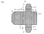
- the RFID module 5 when the RFID module 5 is arranged on the first flap 3g, as shown in FIG. 20, still two other first division slits 10a and the metal film 7 of the first flap 3g
- the second split slit 10b may be formed to reduce the ratio of the first metal region 7a and the second metal region 7b in the first flap 3g.
- the first surface 3a In the region on one side of the first flap 3g where the metal film 7 of the first flap 3g is divided by the slit 9, the first surface 3a continuous with the first metal region 7a of the first flap 3g and the first flap 3g.
- a first dividing slit 10a forming a discontinuous metal region 7c with the first metal region 7a is formed.
- a second split slit 10b is formed which forms a discontinuous metal region 7d with the second metal region 7b of 3a.
- the RFID module 5 and the slit 9 are located between the first division slit 10a and the second division slit 10b.
- the first split slit 10a extends from the margin 3ga at the tip of the first flap 3g toward the first surface 3a in parallel with the slit 9, and is outward at the boundary with the first surface 3a. It bends to extend along the side 3aa between the first flap 3g and the first surface 3a to the upper hypotenuse 3gb.
- the second split slit 10b extends from the margin 3ga at the tip of the first flap 3g toward the first surface 3a in parallel with the slit 9, and is outward at the boundary with the first surface 3a. It bends to extend along the side 3aa between the first flap 3g and the first surface 3a to the lower hypotenuse 3gc.
- the first division slit 10a and the second division slit 10b are arranged on the first flap 3g in line symmetry with respect to the slit 9, for example.
- the first division slit 10a and the second division slit 10b are not limited to the L-shape, but may be curved or linear. Further, the metal in the metal region of the discontinuous metal region 7c and the discontinuous metal region 7d may be eliminated.
- the first flap 3g is provided with the first split slit 10a and the second split slit 10b that reduce the area of the first metal region 7a and the second metal region 7b in the first flap 3g. It is possible to reduce the variation in the characteristics of the capacitive coupling between the respective metal films 7 on the second surface 3b, and it is possible to reduce the variation in the communication characteristics of the container 1H.
- FIG. 21 is a developed view of the container 1J in the modified example.
- the first non-metal region 10c is formed on the side away from the slit 9 from the first metal region 7a, that is, on the upper hypotenuse side 3gb side.
- the second non-metal region 10d is formed on the side away from the slit 9 from the second metal region 7b, that is, on the lower hypotenuse side 3 gc side.
- the first non-metal region 10c and the second non-metal region 10d for example, the first main surface 3s of the base material 3 is exposed, and the adhesive layer 11 is placed on the first non-metal region 10c and the second non-metal region 10d. Is formed so that the front surface (first main surface 3s) of the base material 3 of the first flap 3g and the back surface (second main surface 3t) of the base material 3 of the second surface 3b do not pass through the metal film 7. Can be glued with. Thereby, the adhesive force between the first flap 3g and the second surface 3b can be improved.
- the RFID module 5 is attached to the first metal region 7a and the second metal region 7b, but the present invention is not limited to this.
- the RFIC 23 may be electrically connected to the first metal region 7a and the second metal region 7b via an inductor.
- the inductor is formed on the antenna pattern side.
- the metal film 7 may have a low sheet resistance by attaching a metal foil as in the first embodiment.
- a paint may be applied on a region other than the portion where the RFID module 5 is attached to form a pattern to enhance the design of the container 1. .. Further, the metal film 7 and the slit 9 may be formed on the second main surface 3t instead of the first main surface 3s of the base material 3. That is, the metal film 7 and the slit 9 may be formed inside the container 1.
Landscapes
- Engineering & Computer Science (AREA)
- Physics & Mathematics (AREA)
- Microelectronics & Electronic Packaging (AREA)
- Computer Hardware Design (AREA)
- General Physics & Mathematics (AREA)
- Theoretical Computer Science (AREA)
- Electromagnetism (AREA)
- Mechanical Engineering (AREA)
- Details Of Aerials (AREA)
Abstract
L'invention concerne un récipient comprenant un matériau de base isolant, un film métallique formé sur une première surface principale du matériau de base et une fente formée pour diviser le film métallique en une première région métallique et une seconde région métallique. Le récipient comprend en outre un module RFID comprenant un élément RFID, un circuit de filtre qui transmet, à l'élément RFID, un courant généré par des ondes électromagnétiques ayant une fréquence de résonance unique qui est une fréquence de communication et des première et seconde électrodes connectées au circuit de filtre, la première électrode du module RFID et la première région métallique du film métallique étant électriquement connectées et la seconde électrode du module RFID et la seconde région métallique du film mince étant électriquement connectées.
Priority Applications (2)
| Application Number | Priority Date | Filing Date | Title |
|---|---|---|---|
| JP2022548743A JP7239073B2 (ja) | 2020-10-05 | 2021-10-04 | Rfidモジュールを備えた容器 |
| US18/193,774 US20230259736A1 (en) | 2020-10-05 | 2023-03-31 | Container including rfid module |
Applications Claiming Priority (6)
| Application Number | Priority Date | Filing Date | Title |
|---|---|---|---|
| JP2020168560 | 2020-10-05 | ||
| JP2020-168560 | 2020-10-05 | ||
| JP2021-013692 | 2021-01-29 | ||
| JP2021013692 | 2021-01-29 | ||
| JP2021-105803 | 2021-06-25 | ||
| JP2021105803 | 2021-06-25 |
Related Child Applications (1)
| Application Number | Title | Priority Date | Filing Date |
|---|---|---|---|
| US18/193,774 Continuation US20230259736A1 (en) | 2020-10-05 | 2023-03-31 | Container including rfid module |
Publications (1)
| Publication Number | Publication Date |
|---|---|
| WO2022075263A1 true WO2022075263A1 (fr) | 2022-04-14 |
Family
ID=81126014
Family Applications (1)
| Application Number | Title | Priority Date | Filing Date |
|---|---|---|---|
| PCT/JP2021/036638 WO2022075263A1 (fr) | 2020-10-05 | 2021-10-04 | Récipient comprenant un module rfid |
Country Status (3)
| Country | Link |
|---|---|
| US (1) | US20230259736A1 (fr) |
| JP (1) | JP7239073B2 (fr) |
| WO (1) | WO2022075263A1 (fr) |
Citations (7)
| Publication number | Priority date | Publication date | Assignee | Title |
|---|---|---|---|---|
| JP2000244362A (ja) * | 1999-02-09 | 2000-09-08 | Magnus Granhed | 受動トランスポンダにおけるカプセル化されたアンテナ |
| JP2005149298A (ja) * | 2003-11-18 | 2005-06-09 | Sharp Corp | 無線タグ及びそれを備えた物品並びにrfidシステム |
| WO2014054747A1 (fr) * | 2012-10-05 | 2014-04-10 | 株式会社村田製作所 | Dispositif de terminal de communication |
| JP2015231240A (ja) * | 2014-06-05 | 2015-12-21 | ▲啓▼碁科技股▲ふん▼有限公司 | アンテナ構造とモバイル機器 |
| WO2018164255A1 (fr) * | 2017-03-09 | 2018-09-13 | 株式会社村田製作所 | Dispositif de communication sans fil |
| WO2019039484A1 (fr) * | 2017-08-24 | 2019-02-28 | 株式会社村田製作所 | Emballage avec étiquette rfid |
| WO2019049592A1 (fr) * | 2017-09-05 | 2019-03-14 | 株式会社村田製作所 | Module électronique |
Family Cites Families (10)
| Publication number | Priority date | Publication date | Assignee | Title |
|---|---|---|---|---|
| US6259369B1 (en) | 1999-09-30 | 2001-07-10 | Moore North America, Inc. | Low cost long distance RFID reading |
| JP4580568B2 (ja) | 2001-02-09 | 2010-11-17 | 大日本印刷株式会社 | 非接触icタグ付き収納箱 |
| JP2008107947A (ja) | 2006-10-24 | 2008-05-08 | Toppan Printing Co Ltd | Rfidタグ |
| JP5028176B2 (ja) | 2007-07-25 | 2012-09-19 | 株式会社日立製作所 | Rfidタグ実装パッケージおよびその製造方法 |
| JP5850784B2 (ja) | 2012-03-29 | 2016-02-03 | Dowaエレクトロニクス株式会社 | ブースターアンテナおよびその製造方法 |
| JP7353578B2 (ja) | 2019-03-13 | 2023-10-02 | 大日本印刷株式会社 | Icタグ |
| JP7312355B2 (ja) | 2019-03-27 | 2023-07-21 | 大日本印刷株式会社 | Icタグ、icタグの製造方法、及びic保持部の製造方法 |
| JP7179264B2 (ja) | 2019-03-28 | 2022-11-29 | 大日本印刷株式会社 | Icタグ |
| JP2022056014A (ja) | 2020-09-29 | 2022-04-08 | 大日本印刷株式会社 | Rfタグ付き包装容器 |
| WO2022097422A1 (fr) | 2020-11-09 | 2022-05-12 | 株式会社村田製作所 | Récipient comprenant un module rfid |
-
2021
- 2021-10-04 WO PCT/JP2021/036638 patent/WO2022075263A1/fr active Application Filing
- 2021-10-04 JP JP2022548743A patent/JP7239073B2/ja active Active
-
2023
- 2023-03-31 US US18/193,774 patent/US20230259736A1/en active Pending
Patent Citations (7)
| Publication number | Priority date | Publication date | Assignee | Title |
|---|---|---|---|---|
| JP2000244362A (ja) * | 1999-02-09 | 2000-09-08 | Magnus Granhed | 受動トランスポンダにおけるカプセル化されたアンテナ |
| JP2005149298A (ja) * | 2003-11-18 | 2005-06-09 | Sharp Corp | 無線タグ及びそれを備えた物品並びにrfidシステム |
| WO2014054747A1 (fr) * | 2012-10-05 | 2014-04-10 | 株式会社村田製作所 | Dispositif de terminal de communication |
| JP2015231240A (ja) * | 2014-06-05 | 2015-12-21 | ▲啓▼碁科技股▲ふん▼有限公司 | アンテナ構造とモバイル機器 |
| WO2018164255A1 (fr) * | 2017-03-09 | 2018-09-13 | 株式会社村田製作所 | Dispositif de communication sans fil |
| WO2019039484A1 (fr) * | 2017-08-24 | 2019-02-28 | 株式会社村田製作所 | Emballage avec étiquette rfid |
| WO2019049592A1 (fr) * | 2017-09-05 | 2019-03-14 | 株式会社村田製作所 | Module électronique |
Non-Patent Citations (1)
| Title |
|---|
| ISAO YAMAGUCHI: "Challenges for practical use and possibility of introduction as seen in the demonstration experiment of RFID application in home appliance -UHF band lag that gathers expectations with generally good experimental results-", MATERIAL FLOW, vol. 45, no. 6, 1 June 2004 (2004-06-01), Tokyo, JP, pages 50 - 61, XP009535865, ISSN: 1342-4599 * |
Also Published As
| Publication number | Publication date |
|---|---|
| JPWO2022075263A1 (fr) | 2022-04-14 |
| US20230259736A1 (en) | 2023-08-17 |
| JP7239073B2 (ja) | 2023-03-14 |
Similar Documents
| Publication | Publication Date | Title |
|---|---|---|
| JP7074275B1 (ja) | Rfidモジュールを備えた容器 | |
| JP6414614B2 (ja) | 物品 | |
| KR100920485B1 (ko) | Ic태그 및 그 제조 방법 | |
| JP6583589B2 (ja) | 無線通信デバイス | |
| US7652636B2 (en) | RFID devices having self-compensating antennas and conductive shields | |
| CN212648466U (zh) | Rfic模块及rfid标签 | |
| JP5510560B2 (ja) | 無線通信デバイス | |
| US7857230B2 (en) | Wireless IC device and manufacturing method thereof | |
| JP6590122B1 (ja) | Rfidタグ、および、rfidタグが取り付けられた物品 | |
| JP2011193245A (ja) | アンテナ装置、無線通信デバイス及び無線通信端末 | |
| KR20060004932A (ko) | 자체 보상 안테나 및 전도성 차폐부를 갖는 알에프아이디디바이스 | |
| WO2022075263A1 (fr) | Récipient comprenant un module rfid | |
| EP2309597A1 (fr) | Dispositif RFID avec système d'auto adaptation de l'antenne et écran conducteur | |
| JP2002109492A (ja) | 非接触式データキャリア装置とブースターアンテナ部用配線部材 | |
| WO2022097682A1 (fr) | Récipient pourvu d'un module rfid | |
| JP7197065B2 (ja) | Rfidモジュールを備えた容器 | |
| US20230259735A1 (en) | Container provided with rfid module and method for manufacturing container provided with rfid module | |
| JP7294562B2 (ja) | Rfidモジュールを備えた容器 |
Legal Events
| Date | Code | Title | Description |
|---|---|---|---|
| 121 | Ep: the epo has been informed by wipo that ep was designated in this application |
Ref document number: 21877562 Country of ref document: EP Kind code of ref document: A1 |
|
| ENP | Entry into the national phase |
Ref document number: 2022548743 Country of ref document: JP Kind code of ref document: A |
|
| NENP | Non-entry into the national phase |
Ref country code: DE |
|
| 122 | Ep: pct application non-entry in european phase |
Ref document number: 21877562 Country of ref document: EP Kind code of ref document: A1 |