WO2022071309A1 - 光導波路素子、および光変調器 - Google Patents
光導波路素子、および光変調器 Download PDFInfo
- Publication number
- WO2022071309A1 WO2022071309A1 PCT/JP2021/035616 JP2021035616W WO2022071309A1 WO 2022071309 A1 WO2022071309 A1 WO 2022071309A1 JP 2021035616 W JP2021035616 W JP 2021035616W WO 2022071309 A1 WO2022071309 A1 WO 2022071309A1
- Authority
- WO
- WIPO (PCT)
- Prior art keywords
- optical waveguide
- substrate
- base layer
- electrode
- light
- Prior art date
- Legal status (The legal status is an assumption and is not a legal conclusion. Google has not performed a legal analysis and makes no representation as to the accuracy of the status listed.)
- Ceased
Links
Images




Classifications
-
- G—PHYSICS
- G02—OPTICS
- G02F—OPTICAL DEVICES OR ARRANGEMENTS FOR THE CONTROL OF LIGHT BY MODIFICATION OF THE OPTICAL PROPERTIES OF THE MEDIA OF THE ELEMENTS INVOLVED THEREIN; NON-LINEAR OPTICS; FREQUENCY-CHANGING OF LIGHT; OPTICAL LOGIC ELEMENTS; OPTICAL ANALOGUE/DIGITAL CONVERTERS
- G02F1/00—Devices or arrangements for the control of the intensity, colour, phase, polarisation or direction of light arriving from an independent light source, e.g. switching, gating or modulating; Non-linear optics
- G02F1/01—Devices or arrangements for the control of the intensity, colour, phase, polarisation or direction of light arriving from an independent light source, e.g. switching, gating or modulating; Non-linear optics for the control of the intensity, phase, polarisation or colour
- G02F1/21—Devices or arrangements for the control of the intensity, colour, phase, polarisation or direction of light arriving from an independent light source, e.g. switching, gating or modulating; Non-linear optics for the control of the intensity, phase, polarisation or colour by interference
- G02F1/225—Devices or arrangements for the control of the intensity, colour, phase, polarisation or direction of light arriving from an independent light source, e.g. switching, gating or modulating; Non-linear optics for the control of the intensity, phase, polarisation or colour by interference in an optical waveguide structure
- G02F1/2255—Devices or arrangements for the control of the intensity, colour, phase, polarisation or direction of light arriving from an independent light source, e.g. switching, gating or modulating; Non-linear optics for the control of the intensity, phase, polarisation or colour by interference in an optical waveguide structure controlled by a high-frequency electromagnetic component in an electric waveguide structure
-
- G—PHYSICS
- G02—OPTICS
- G02F—OPTICAL DEVICES OR ARRANGEMENTS FOR THE CONTROL OF LIGHT BY MODIFICATION OF THE OPTICAL PROPERTIES OF THE MEDIA OF THE ELEMENTS INVOLVED THEREIN; NON-LINEAR OPTICS; FREQUENCY-CHANGING OF LIGHT; OPTICAL LOGIC ELEMENTS; OPTICAL ANALOGUE/DIGITAL CONVERTERS
- G02F1/00—Devices or arrangements for the control of the intensity, colour, phase, polarisation or direction of light arriving from an independent light source, e.g. switching, gating or modulating; Non-linear optics
- G02F1/01—Devices or arrangements for the control of the intensity, colour, phase, polarisation or direction of light arriving from an independent light source, e.g. switching, gating or modulating; Non-linear optics for the control of the intensity, phase, polarisation or colour
- G02F1/03—Devices or arrangements for the control of the intensity, colour, phase, polarisation or direction of light arriving from an independent light source, e.g. switching, gating or modulating; Non-linear optics for the control of the intensity, phase, polarisation or colour based on ceramics or electro-optical crystals, e.g. exhibiting Pockels effect or Kerr effect
- G02F1/0305—Constructional arrangements
- G02F1/0316—Electrodes
-
- G—PHYSICS
- G02—OPTICS
- G02F—OPTICAL DEVICES OR ARRANGEMENTS FOR THE CONTROL OF LIGHT BY MODIFICATION OF THE OPTICAL PROPERTIES OF THE MEDIA OF THE ELEMENTS INVOLVED THEREIN; NON-LINEAR OPTICS; FREQUENCY-CHANGING OF LIGHT; OPTICAL LOGIC ELEMENTS; OPTICAL ANALOGUE/DIGITAL CONVERTERS
- G02F1/00—Devices or arrangements for the control of the intensity, colour, phase, polarisation or direction of light arriving from an independent light source, e.g. switching, gating or modulating; Non-linear optics
- G02F1/01—Devices or arrangements for the control of the intensity, colour, phase, polarisation or direction of light arriving from an independent light source, e.g. switching, gating or modulating; Non-linear optics for the control of the intensity, phase, polarisation or colour
- G02F1/03—Devices or arrangements for the control of the intensity, colour, phase, polarisation or direction of light arriving from an independent light source, e.g. switching, gating or modulating; Non-linear optics for the control of the intensity, phase, polarisation or colour based on ceramics or electro-optical crystals, e.g. exhibiting Pockels effect or Kerr effect
- G02F1/035—Devices or arrangements for the control of the intensity, colour, phase, polarisation or direction of light arriving from an independent light source, e.g. switching, gating or modulating; Non-linear optics for the control of the intensity, phase, polarisation or colour based on ceramics or electro-optical crystals, e.g. exhibiting Pockels effect or Kerr effect in an optical waveguide structure
-
- G—PHYSICS
- G02—OPTICS
- G02F—OPTICAL DEVICES OR ARRANGEMENTS FOR THE CONTROL OF LIGHT BY MODIFICATION OF THE OPTICAL PROPERTIES OF THE MEDIA OF THE ELEMENTS INVOLVED THEREIN; NON-LINEAR OPTICS; FREQUENCY-CHANGING OF LIGHT; OPTICAL LOGIC ELEMENTS; OPTICAL ANALOGUE/DIGITAL CONVERTERS
- G02F1/00—Devices or arrangements for the control of the intensity, colour, phase, polarisation or direction of light arriving from an independent light source, e.g. switching, gating or modulating; Non-linear optics
- G02F1/01—Devices or arrangements for the control of the intensity, colour, phase, polarisation or direction of light arriving from an independent light source, e.g. switching, gating or modulating; Non-linear optics for the control of the intensity, phase, polarisation or colour
- G02F1/21—Devices or arrangements for the control of the intensity, colour, phase, polarisation or direction of light arriving from an independent light source, e.g. switching, gating or modulating; Non-linear optics for the control of the intensity, phase, polarisation or colour by interference
- G02F1/212—Mach-Zehnder type
Definitions
- the present invention relates to an optical waveguide element which is a functional element using an optical waveguide and an optical modulator using an optical modulation element which is an optical waveguide element.
- the light modulation element using LiNbO 3 (hereinafter, also referred to as LN) having an electro-optical effect as a substrate uses a semiconductor material such as indium phosphorus (InP), silicon (Si), or gallium arsenide (GaAs). It is widely used in high-speed / large-capacity optical fiber communication systems because it has less light loss and can realize wide-band optical modulation characteristics as compared with the light modulation elements.
- the modulation method in the optical fiber communication system is QPSK (Quadrature Phase Shift Keying), DP-QPSK (Dual Phaseization-Quadrature Phase Shift Keying), etc. in response to the trend of increasing transmission capacity in recent years. Transmission formats that incorporate phase shift keying into multi-value modulation are the mainstream.
- the film is made thinner in order to strengthen the interaction between the signal electric field and the waveguide light in the substrate (that is, to increase the electric field efficiency).
- a convex optical waveguide configured by forming a band-shaped convex portion on the surface of an LN substrate (for example, a thickness of 20 ⁇ m or less).
- Modulators are also being put into practical use (for example, Patent Documents 1 and 2).
- Au gold
- Ti titanium
- an optical waveguide element using a convex optical waveguide such as a rib type optical waveguide or a ridge type optical waveguide, it is possible to suppress the occurrence of loss in the propagating light due to an electrode provided in the vicinity of the convex optical waveguide. Is required.
- One aspect of the present invention is an optical waveguide element having a substrate on which an optical waveguide is formed and an electrode formed on the substrate for controlling a light wave propagating through the optical waveguide, wherein the optical waveguide element is provided.
- the waveguide is composed of a convex portion extending on the substrate
- the electrode is composed of a base layer composed of Nb between the waveguide and the substrate layer and an upper layer formed on the base layer.
- the base layer has a thickness of 30 nm or less.
- the underlayer is either formed on the substrate containing oxygen atoms or formed on a film of oxide formed on the substrate.
- the base layer contains oxygen atoms and has an element ratio Nb / O of Nb to oxygen of 1.0 or more.
- the electrode is composed of a plurality of electrodes arranged along the optical waveguide at positions sandwiching the optical waveguide on the substrate.
- Another aspect of the present invention includes any of the above optical waveguide elements, which are optical waveguide elements that modulate light, a housing that houses the optical waveguide elements, an optical fiber that inputs light to the optical waveguide elements, and the above.
- An optical modulator comprising an optical fiber that guides the light output by the optical waveguide element to the outside of the housing.
- this specification shall include all the contents of the Japanese patent application / Japanese Patent Application No. 2020-164627 filed on September 30, 2020.
- an optical waveguide element using a convex optical waveguide such as a rib type optical waveguide or a ridge type optical waveguide
- a loss occurs in propagating light due to an electrode provided in the vicinity of the convex optical waveguide. It can be effectively suppressed.
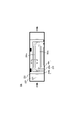
- FIG. 1 is a diagram showing a configuration of an optical modulator according to an embodiment of the present invention.
- FIG. 2 is a diagram showing a configuration of a light modulation element used in the light modulator shown in FIG.
- FIG. 3 is a cross-sectional view taken along the line III-III of the light modulation element shown in FIG.
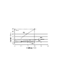
- FIG. 4 is a diagram showing simulation results of light absorption loss when various metals are used for the base layer of the electrode.
- FIG. 5 is a diagram showing the evaluation results of the adhesion strength of the electrode to the substrate when various metals are used for the base layer of the electrode.
- FIG. 6 is a diagram showing the results of composition analysis in the cross section of the electrode constituent portion when the electrode including the base layer of Nb is configured on the substrate.
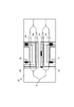
- FIG. 7 is a diagram showing another example of the light modulation element according to the present invention.
- the optical waveguide element according to the embodiment shown below is a light modulation element configured by using an LN substrate, but the optical waveguide element according to the present invention is not limited to this.
- the present invention can be similarly applied to an optical waveguide element using a substrate other than the LN substrate and an optical waveguide element having a function other than optical modulation.
- FIG. 1 is a diagram showing a configuration of an optical modulation element, which is an optical waveguide element according to an embodiment of the present invention, and an optical modulator.
- the optical waveguide element is an optical modulation element 102 that performs optical modulation using the Machzenda optical waveguide.
- the light modulator 100 accommodates the light modulation element 102 inside the housing 104.
- a cover (not shown), which is a plate body, is fixed to the opening of the housing 104, and the inside thereof is hermetically sealed.
- the light modulator 100 has an input optical fiber 106 for inputting light into the housing 104, and an output optical fiber 108 for guiding the light modulated by the light modulation element 102 to the outside of the housing 104.
- the light modulator 100 also has a connector 110 for receiving a high frequency electric signal for causing the light modulation element 102 to perform an optical modulation operation from the outside, and a high frequency electric signal received by the connector 110 of the light modulation element 102.
- a relay board 112 for relaying to one end of an electrode (for example, a signal electrode) is provided.
- the light modulator 100 includes a terminator 114 having a predetermined impedance, which is connected to the other end of the electrode of the light modulation element 102.
- the electrodes of the light modulation element 102 and the relay board 112 and the terminator 114 are electrically connected by bonding, for example, a metal wire.
- FIG. 2 is a diagram showing the configuration of the light modulation element 102, which is an optical waveguide element housed in the housing 104 of the light modulator 100 shown in FIG.
- the light modulation element 102 is composed of an optical waveguide 224 formed on the substrate 220.
- the substrate 220 is, for example, an X-cut LN substrate having an electro-optic effect, which is processed to a thickness of 20 ⁇ m or less (for example, 2 ⁇ m) and thinned.
- the optical waveguide is a convex optical waveguide (for example, a rib-type optical waveguide or a ridge-type optical waveguide) formed on the surface of a thin-film substrate 220 and composed of convex portions extending in a band shape.
- a convex optical waveguide for example, a rib-type optical waveguide or a ridge-type optical waveguide
- glass is generally provided via an adhesive layer 350 (described later) in order to reinforce the mechanical strength of the entire substrate. Etc. are adhered to the support plate 222.
- the optical waveguide 224 is, for example, a Machzenda optical waveguide, which includes two branch portions and two parallel waveguides 226a and 226b extending in parallel with each other. Electrodes 230a, 230b, 230c are also provided on the substrate 220 to control the light waves propagating in the parallel waveguides 226a and 226b by changing the refractive index of the parallel waveguides 226a and 226b.
- the electrodes 230a, 230b, and 230c are collectively referred to as an electrode 230.
- the electrode 230 constitutes, for example, a coplanar transmission line having a predetermined impedance according to the prior art.
- the electrode 230a is a center electrode, and is formed at a position sandwiched between the parallel waveguides along the parallel waveguides 226a and 226b in the plane of the substrate 220.
- the electrodes 230b and 230c are ground electrodes, and are formed along the parallel waveguides at positions facing the electrodes 230a with the parallel waveguides 226a and 226b, respectively.
- the electrode 230 Since the lower right end of the substrate 220 is terminated by the terminator 114, the electrode 230 transmits a high frequency signal input from the lower left end of the board 220 via the connector 110 from the left to the right in the figure. Propagate as a traveling wave. As a result, the electrode 230 constitutes a signal line that controls the light wave propagating from the left side to the right side of the parallel waveguides 226a and 226b.
- FIG. 3 is a sectional view taken along line III-III of the light modulation element 102 shown in FIG.
- the substrate 220 is adhered to a support plate 222, which is glass, for example, via an adhesive layer 350.
- the parallel waveguide 226a which is a convex optical waveguide, is composed of a convex portion 300 formed on the substrate 220.
- the height t1 of the convex portion 300 measured from the surface of the substrate 220 is 10 ⁇ m or less (for example, 1 ⁇ m).
- Electrodes 230a and 230b are arranged on the substrate 220 with the parallel waveguide 226a interposed therebetween. Both the electrode 230a and the electrode 230b are formed on the substrate 220 at a height t2. The height t2 is set so that the electrode 230 has a predetermined impedance and the traveling wave of the high-frequency electric signal propagating through the electrode 230 propagates at a predetermined speed with a loss within a predetermined range.
- the distance w2 between the electrode 230a and the electrode 230b, whichever is closer to the parallel waveguide 226a (the electrode 230a in this embodiment), and the parallel waveguide 226a is, for example, 0.5 times or more and twice or less the w1. (That is, 0.5w1 ⁇ w2 ⁇ 2w1).
- the electrode 230a and the electrode 230b are configured around the parallel waveguide 226a, the distance between the electrodes 230a and 230b and the parallel waveguide 226a is set to be different.
- the intervals w2 are the same as each other.
- the electrodes 230a and 230b have similar configurations to each other, and are composed of upper layers 302a and 302b and base layers 304a and 304b, respectively.
- the electrode 230c is not shown in FIG. 3, it should be understood that the electrode 230c is also composed of an upper layer and a base layer similar to the electrodes 230a and 230b.
- the upper layers 302a and 302b and the upper layer of the electrode 230c are collectively referred to as an upper layer 302
- the base layers 304a and 304b and the base layer of the electrode 230c are collectively referred to as a base layer 304.
- the electrode 230 is composed of an upper layer 302 and a base layer 304.
- the upper layer 302 is made of, for example, Au (gold), as in the prior art.
- Au constituting the upper layer 302 does not have sufficient adhesive strength to the substrate 220 when it is directly formed on the substrate 220, and therefore is formed on the substrate 220 via the base layer 304.
- the base layer provided to secure the adhesion strength to the substrate is generally composed of Ti (titanium).
- Ti titanium
- the inventor of the present invention absorbs the light propagating through the convex optical waveguide by the metal constituting the base layer of the electrode, thereby absorbing the convex optical waveguide. It was found that a loss (light absorption loss) occurs in the propagating light of.
- the inventor of the present invention causes such a light absorption loss as the operating light wavelength of the optical modulation element (for example, the light wavelength of 1.55 ⁇ m used for optical communication and / or) in the light absorption spectrum of the metal of the underlying layer. It was found that 1.3 ⁇ m) exists in the light absorption region, and that a part of the mode field of the propagating light propagating in the convex optical waveguide extends to the substrate part near the convex waveguide. rice field.
- the operating light wavelength of the optical modulation element for example, the light wavelength of 1.55 ⁇ m used for optical communication and / or
- the underlying layer needs to be made of a metal having good adhesion strength and not including the operating light wavelength in the light absorption region, and to be formed with a thickness capable of suppressing the light absorption loss to a certain level or less. be.
- the inventor of the present invention has repeatedly studied the material and thickness of the base layer, and as a solution for suppressing the light absorption loss as described above while maintaining the adhesion strength to the substrate at a practical level, a metal for the base layer. It was found that it is effective to use Nb (niobium) instead of Ti which has been conventionally used.
- the base layer 304 is composed of Nb having a film thickness of t3.
- the formation of the base layer and the upper layer on the substrate 220 can be performed by, for example, electron beam vapor deposition (EB vapor deposition).
- EB vapor deposition electron beam vapor deposition
- FIG. 4 is a part of the simulation result of the amount of increase in light absorption loss with respect to the thickness of the base layer 304 when various metals are used as the base layer 304.
- FIG. 4 shows the calculation results when Ti, Al (aluminum), and Nb are used as the base layer 304 in addition to the case where the base layer 304 is not used (in the case of Au (upper layer 302) single film). Has been done.
- the horizontal axis is the thickness t3 of the base layer 304
- the vertical axis is the amount of light absorption loss when propagating the unit length (1 cm) of the parallel waveguide 226a.
- the model used for the simulation is the same as the configuration shown in FIG.
- the light absorption loss ⁇ 0 in the case of the Au single film shown in line 400 is the light absorption loss as a background in the above configuration, and the increase in the light absorption loss from this reference line is used.
- the light absorption loss in the base layer 304 can be evaluated.
- Lines 402, 404, and 406 show the light absorption loss when the metal constituting the base layer 304 is composed of Ti, Al, and Nb, respectively.
- Ti shown by line 402 has the largest light absorption loss, and the light absorption loss increases greatly with the film thickness.
- the light absorption loss can be significantly reduced as compared with the case of Ti (line 402). I understand.
- the base layer 304 is Al (line 404)
- the light absorption loss is the smallest, and the light absorption loss is substantially constant with respect to the thickness of the base layer.
- Al has a low adhesion strength to the substrate.
- FIG. 5 is a table showing the results of evaluating the adhesion strength of the electrode to the LN substrate when various metals are used as the base layer.
- the upper layer was Au with a thickness of 100 nm.
- the evaluation of the adhesive strength was in accordance with Japanese Industrial Standards JIS K 5600-5-6: 1999. That is, after forming a layer of electrodes on the entire substrate surface of the LN substrate, a cutter is used to make a cut in the electrodes to form 10 ⁇ 10 (100 in total) rectangular samples of the same size on the plane of the LN substrate. do.
- an adhesive tape having the adhesiveness specified in the above standard is attached onto the above 100 samples, and when the tape is peeled off from the LN substrate, it is fixed by the number of samples remaining on the LN substrate. The strength was evaluated.
- the base layer and the upper layer were formed on the LN substrate by using EB vapor deposition.
- the sample 01 shown in FIG. 5 is a sample of an Au single film (no base layer, only the upper layer), and the adhesion rate is 0%.
- Samples 02 to 04 are samples using conventional Ti as the base layer, and have an adhesion rate of 100% when the thickness of the base layer is 1 ⁇ m or more.
- the adhesion rate is less than 100% at any thickness, and the fixing strength at a level that can withstand practical use cannot be obtained.
- the adhesion rate is 100% at a thickness of 1 ⁇ m or more, and it can be seen that a practically sufficient fixing strength can be obtained.
- FIG. 6 is a result of cross-sectional composition analysis of the portion where these electrodes are formed in the sample in which the base layer of Nb and the upper layer of Au are formed on the LN substrate. Similar to the evaluation in FIG. 5, the base layer and the upper layer are formed by using EB vapor deposition. The horizontal axis of FIG. 6 is the position, and the vertical axis is the composition ratio (atomic percent). Further, in FIG. 6, lines 610, 612, and 614 show position changes in the composition ratios of oxygen, Nb, and Au, respectively.
- the elemental ratio Nb / O of Nb to oxygen in the base layer of Nb is 1.2.
- the Nb oxide can take various forms such as NbO and NbO 2
- the element ratio Nb / O in the base layer of Nb may be substantially 1.0 or more. .2 or more is considered preferable.
- the oxygen present in the vicinity of the interface 602 in the underlayer of Nb is due to the permeation of oxygen from the LN substrate or the permeation of oxygen existing in the environmental atmosphere into the underlayer. ..
- the base layer 304 is composed of Nb, and the elemental ratio of Nb to oxygen in the base layer 304 is 1.2.
- the thickness of the base layer composed of Nb is 30 nm or less. If the thickness of the underlayer of Nb is within this range, the light absorption loss is 2 ⁇ 0 or less, which is twice the value of ⁇ 0 for Au single film, or the value for the underlayer using conventional Ti. It can be suppressed to a value of 1/3 or less with respect to about 6 ⁇ 0 .
- w2 2.0 ⁇ m
- the thickness t3 of the base layer 304 composed of Nb is, for example, 10 nm. At this time, the light absorption loss in the parallel waveguide 226a is 6.0 dB / cm.
- the adhesion strength of the electrode 230 to the substrate 220 is practically used. It is possible to effectively suppress the light absorption loss in the parallel waveguide 226a to 1/3 or less as compared with the conventional optical waveguide element using Ti as the base layer while maintaining the level that can withstand the above.
- the present invention is not limited to the configuration of the above embodiment and its modifications, and can be implemented in various embodiments without departing from the gist thereof.
- the substrate 220 is an LN substrate, but the material of the substrate 220 is not limited to the LN.
- the substrate 220 on which the base layer 304 composed of Nb is formed may be composed of a material containing oxygen in its composition, for example, lithium tantalate (LiTaO 3 ).
- the substrate 220 may be a semiconductor such as InP or so-called silicon photonics.
- -It may be a Si substrate used for the device.
- the base layer 304 and the upper layer 302 of the electrode 230 are formed by EB vapor deposition, but the means for forming the electrode 230 is not limited to EB vapor deposition.
- the base layer 304 and the upper layer 302 of the electrode 230 may be formed by a vapor deposition method other than EB vapor deposition, a sputtering method, or the like.
- the light modulation element 102 an optical modulation element in which the optical modulation operation is performed by the optical waveguide 224 constituting a single Machzenda optical waveguide including a pair of parallel waveguides 226a and 226b is shown.
- the configuration of the electrode shown as an example in the electrode 230 is not limited to the light modulation element composed of a single Machzenda optical waveguide.
- the electrode having the same base layer 304 as the above-mentioned electrode 230 shown in FIG. 3 is a light for DP-QPSK modulation, which is configured by using two so-called nested Machzenda optical waveguides as shown in FIG. 7, for example. It can be similarly used for the modulation element 702.
- the electrodes 730a extending along the parallel waveguides 726a, 726b, 726c, 726d (dashed line in the figure), which are convex optical waveguides formed on the substrate 720 similar to the substrate 220, respectively.
- the 730b, 730c, and 730d can be composed of an upper layer 302 and a base layer 304 similar to the electrode 230 shown in FIG. As a result, even in the light modulation element that performs such DP-QPSK modulation, the light absorption loss in the parallel waveguide 726a or the like can be reduced, and good modulation characteristics can be obtained.
- the light modulation element 102 which is the optical waveguide element shown in the present embodiment, is a light wave propagating through the substrate 220 on which the optical waveguide 224 is formed and the optical waveguide 224 formed on the substrate 220. It has an electrode 230 for controlling the above.
- the optical waveguide 224 is composed of a convex portion (for example, a convex portion 300) extending on the substrate 220.
- the electrode 230 is composed of a base layer 304 formed of Nb between the electrode 230 and the substrate 220, and an upper layer 302 formed on the base layer 304.
- the light absorption loss due to the presence of the electrode 230 is effectively reduced in the optical waveguide 224 (for example, the parallel waveguide 226a) which is a convex optical waveguide. Can be reduced.
- the base layer 304 has a thickness of 30 nm or less. According to this configuration, the light absorption loss generated in the optical waveguide 224 due to the presence of the electrode 230 can be reduced to 1/3 as compared with the conventional configuration using the Ti base layer.
- the base layer 304 is formed on the substrate 220 containing oxygen atoms, or is formed on the oxide film formed on the substrate 220. According to this configuration, it is possible to secure a level of fixing force that can withstand practical use between the base layer 304 made of Nb and the substrate made of LN or the like.
- the base layer 304 contains oxygen atoms, and the element ratio Nb / O of Nb to oxygen is 1.0 or more. According to this configuration, it is possible to more reliably secure a level of fixing force that can withstand practical use between the base layer 304 made of Nb and the substrate made of LN or the like.
- the electrodes 230 are a plurality of (for example, two) electrodes 230a and 230b arranged along the parallel waveguide 226a on the substrate 220 at positions sandwiching the parallel waveguide 226a constituting the optical waveguide 224, for example. It is composed. According to this configuration, it is possible to effectively suppress the occurrence of light absorption loss in the propagating light of the parallel waveguide 226a due to the electrodes arranged close to each other with the parallel waveguide 226a interposed therebetween.
- the light modulation element 102 which is an optical waveguide element
- the housing 104 accommodating the light modulation element 102
- the input optical fiber 106 which inputs light to the light modulation element 102
- the housing 104 which outputs the light output by the light modulation element 102.
- the light modulator 100 can be configured by the output optical fiber 108 that leads to the outside of the above.
- the light modulator 100 configured in this way uses the light modulation element 102 in which the light absorption loss in the convex optical waveguide (for example, the parallel waveguide 226a) that may occur due to the presence of the electrode 230 is suppressed. Therefore, good optical modulation characteristics and optical transmission characteristics can be realized.
Landscapes
- Physics & Mathematics (AREA)
- Nonlinear Science (AREA)
- General Physics & Mathematics (AREA)
- Optics & Photonics (AREA)
- Electromagnetism (AREA)
- Chemical & Material Sciences (AREA)
- Engineering & Computer Science (AREA)
- Ceramic Engineering (AREA)
- Crystallography & Structural Chemistry (AREA)
- Optical Modulation, Optical Deflection, Nonlinear Optics, Optical Demodulation, Optical Logic Elements (AREA)
- Optical Integrated Circuits (AREA)
Abstract
本発明は、凸状光導波路を用いる光導波路素子において、伝搬光を制御する電極の存在により伝搬光に損失が発生するのを効果的に抑制することを目的とする。 本発明の光導波路素子は、光導波路(226a)が形成された基板(220)と、基板の上に形成された、光導波路を伝搬する光波を制御する電極(230a、230b)と、を有する光導波路素子であって、上記光導波路(226a)は基板上に延在する凸部(300)により構成され、電極(230a、230b)は、上記基板との間にNbで構成される下地層(304a、304b)と、下地層の上に形成された上部層(302a、302b)と、で構成されている。
Description
本発明は、光導波路を用いた機能素子である光導波路素子、及び光導波路素子である光変調素子を用いた光変調器に関する。
高速/大容量光ファイバ通信システムにおいては、導波路型の光変調器を組み込んだ光送信装置が多く用いられている。中でも、電気光学効果を有するLiNbO3(以下、LNともいう)を基板に用いた光変調素子は、インジウムリン(InP)、シリコン(Si)、あるいはガリウム砒素(GaAs)などの半導体系材料を用いた光変調素子に比べて、光の損失が少なく且つ広帯域な光変調特性を実現し得ることから、高速/大容量光ファイバ通信システムに広く用いられている。
一方、光ファイバ通信システムにおける変調方式は、近年の伝送容量の増大化の流れを受け、QPSK(Quadrature Phase Shift Keying)やDP-QPSK(Dual Polarization - Quadrature Phase Shift Keying)等、多値変調や、多値変調に偏波多重を取り入れた伝送フォーマットが主流となっている。
近年のインターネットサービスの普及加速は通信トラフィックのより一層の増大を招き、光変調素子の更なる小型化、広帯域化、省電力化の検討が今も進められている。
そのような光変調素子の小型化、広帯域化、省電力化の一つの策として、基板中における信号電界と導波光との相互作用をより強めるべく(すなわち、電界効率を高めるべく)薄膜化したLN基板(例えば、厚さ20μm以下)の表面に帯状の凸部を形成することで構成されるリブ型光導波路またはリッジ型光導波路(以下、総称して凸状光導波路という)を用いた光変調器も実用化されつつある(例えば、特許文献1、2)。
現在では、さらなる高速化のため、電界効率を更に高めるべく、凸状光導波路の位置により近接して電極を設ける検討も進められている。電極の構造としてはAu(金)が主に用いられるが、Auは、LN基板に対する密着性が低く、実用上十分な固着強度を得られないことから、一般的には、電極の下地層としてTi(チタン)の膜を形成することで、基板に対する電極の固着強度が確保される。
しかしながら、本発明の発明者の知見では、上記の構成を有する従来の電極をリブ型光導波路の位置により近接して設けた場合には、凸状光導波路を伝搬する光波に顕著な光損失が発生し得る。
上記背景より、リブ型光導波路やリッジ型光導波路等の凸状光導波路を用いる光導波路素子において、凸状光導波路に近接して設けられた電極により伝搬光に損失が発生するのを抑制することが求められている。
本発明の一の態様は、光導波路が形成された基板と、前記基板の上に形成された、前記光導波路を伝搬する光波を制御する電極と、を有する光導波路素子であって、前記光導波路は、前記基板上に延在する凸部により構成され、前記電極は、前記基板との間にNbで構成される下地層と、下地層の上に形成された上部層と、で構成されている。
本発明の他の態様によると、前記下地層は、30nm以下の厚さである。
本発明の他の態様によると、前記下地層は、酸素原子を含む前記基板上に形成されるか、または前記基板上に形成された酸化物の膜の上に形成される。
本発明の他の態様によると、前記下地層は、酸素原子を含み、酸素に対するNbの元素比率Nb/Oが1.0以上である。
本発明の他の態様によると、前記電極は、前記基板上において、前記光導波路を挟む位置に当該光導波路に沿って配された複数の電極で構成される。
本発明の他の態様は、光の変調を行う光変調素子である上記いずれかの光導波路素子と、光導波路素子を収容する筺体と、前記光導波路素子に光を入力する光ファイバと、前記光導波路素子が出力する光を前記筺体の外部へ導く光ファイバと、を備える光変調器である。
なお、この明細書には、2020年9月30日に出願された日本国特許出願・特願2020-164627号の全ての内容が含まれるものとする。
本発明の他の態様によると、前記下地層は、30nm以下の厚さである。
本発明の他の態様によると、前記下地層は、酸素原子を含む前記基板上に形成されるか、または前記基板上に形成された酸化物の膜の上に形成される。
本発明の他の態様によると、前記下地層は、酸素原子を含み、酸素に対するNbの元素比率Nb/Oが1.0以上である。
本発明の他の態様によると、前記電極は、前記基板上において、前記光導波路を挟む位置に当該光導波路に沿って配された複数の電極で構成される。
本発明の他の態様は、光の変調を行う光変調素子である上記いずれかの光導波路素子と、光導波路素子を収容する筺体と、前記光導波路素子に光を入力する光ファイバと、前記光導波路素子が出力する光を前記筺体の外部へ導く光ファイバと、を備える光変調器である。
なお、この明細書には、2020年9月30日に出願された日本国特許出願・特願2020-164627号の全ての内容が含まれるものとする。
本発明によれば、リブ型光導波路やリッジ型光導波路等の凸状光導波路を用いる光導波路素子において、凸状光導波路に近接して設けられた電極により伝搬光に損失が発生するのを効果的に抑制することができる。
以下、本発明の実施形態について、図面を参照して説明する。なお、以下に示す実施形態に係る光導波路素子は、LN基板を用いて構成される光変調素子であるが、本発明に係る光導波路素子は、これには限られない。本発明は、LN基板以外の基板を用いる光導波路素子や、光変調以外の機能を有する光導波路素子にも、同様に適用することができる。
図1は、本発明の一実施形態に係る光導波路素子である光変調素子、および光変調器の構成を示す図である。本実施形態では、光導波路素子はマッハツェンダ光導波路を用いて光変調を行う光変調素子102である。
光変調器100は、筺体104の内部に光変調素子102を収容する。なお、筺体104は、最終的にはその開口部に板体であるカバー(不図示)が固定されて、その内部が気密封止される。
光変調器100は、筺体104内に光を入力するための入力光ファイバ106と、光変調素子102により変調された光を筺体104の外部へ導く出力光ファイバ108と、を有する。
光変調器100は、また、光変調素子102に光変調動作を行わせるための高周波電気信号を外部から受信するためのコネクタ110と、当該コネクタ110が受信した高周波電気信号を光変調素子102の電極(例えば、信号用電極)の一端へと中継するための中継基板112を備える。また、光変調器100は、光変調素子102の電極の他端に接続される、所定のインピーダンスを有する終端器114を備える。ここで、光変調素子102の電極と、中継基板112及び終端器114と、の間は、例えば金属ワイヤ等のボンディングにより電気的に接続される。
図2は、図1に示す光変調器100の筺体104に収容される光導波路素子である光変調素子102の構成を示す図である。光変調素子102は、基板220上に形成された光導波路224で構成されている。基板220は、例えば、20μm以下(例えば2μm)の厚さに加工され薄膜化された、電気光学効果を有するXカットのLN基板である。
光導波路は、薄膜化された基板220の表面に形成された、帯状に延在する凸部で構成された凸状光導波路(例えば、リブ型光導波路又はリッジ型光導波路)である。ここで、LN基板は、応力が加わると光弾性効果により屈折率が局所的に変化し得るため、基板全体の機械強度を補強すべく、一般的には接着層350(後述)を介してガラス等の支持板222に接着されている。
光導波路224は、例えばマッハツェンダ光導波路であり、2つの分岐部と、互いに並行に延在する2本の並行導波路226a、226bとを含む。基板220上には、また、並行導波路226a、226bの屈折率を変化させて当該並行導波路226a、226bを伝搬する光波を制御する電極230a、230b、230cが設けられている。以下、電極230a、230b、230cを総称して電極230ともいう。
電極230は、従来技術に従い、例えば、所定のインピーダンスを有するコプレーナ伝送線路を構成している。具体的には、電極230aは、中心電極であり、基板220の面内において並行導波路226a、226bに沿うように、これら並行導波路の間に挟まれる位置に形成されている。また、電極230bおよび230cは、接地電極であり、それぞれ、並行導波路226a及び226bを挟んで電極230aと対向する位置に、これら並行導波路に沿って形成されている。
電極230は、基板220の図示右下の末端が終端器114で終端されていることにより、コネクタ110を介して基板220の図示左下の末端から入力される高周波信号を、図示左方から右方へ進行波として伝搬させる。これにより、電極230は、並行導波路226a、226bを図示左方から右方へ伝搬する光波を制御する信号線路を構成する。
図3は、図2に示す光変調素子102のIII-III断面矢視図である。基板220は、接着層350を介して、例えばガラスである支持板222に接着されている。凸状光導波路である並行導波路226aは、基板220に形成された凸部300により構成されている。基板220の面から測った凸部300の高さt1は、10μm以下(例えば1μm)である。
基板220上には、並行導波路226aを挟んで電極230a及び230bが配されている。電極230aおよび電極230bは、共に、基板220上に高さt2で形成されている。この高さt2は、電極230が所定のインピーダンスを持つように、及び電極230を伝搬する高周波電気信号の進行波が所定範囲内の損失で且つ所定の速度で伝搬するように、設定される。
電極230a及び電極230bのうち、いずれか並行導波路226aに近い方の電極(本実施形態では電極230a)と、並行導波路226aとの間隔w2は、例えばw1の0.5倍以上2倍以下(すなわち、0.5w1≦w2≦2w1)である。なお、当然ながら、電極230aと電極230bとが並行導波路226aを中心として対象に構成されている場合には、電極230a及び電極230bと、並行導波路226aと、の間のそれぞれの間隔は、互いに同じ間隔w2となる。
電極230a及び電極230bは、互いに同様の構成を有しており、それぞれ、上部層302a及び302bと、下地層304a及び304bと、により構成されている。ここで、図3には、電極230cは示されていないが、電極230cも、電極230a及び電極230bと同様の上部層及び下地層で構成されているものと理解されたい。
以下、上部層302a、302b及び図示しない電極230cの上部層を総称して上部層302ともいい、下地層304a、304b及び図示しない電極230cの下地層を総称して下地層304ともいうものとする。すなわち、電極230は、上部層302と、下地層304と、で構成されている。
上部層302は、従来技術と同様に、例えばAu(金)で構成される。上部層302を構成するAuは、基板220上に直接形成した場合には基板220に対して実用上十分な固着強度を持たないことから、下地層304を介して基板220上に形成される。
従来、基板との固着強度を確保するために設けられる下地層は、一般的にはTi(チタン)で構成される。本発明の発明者は、凸状光導波路の近傍に電極が設けられる場合、その電極の下地層を構成する金属により、凸状光導波路を伝搬する光が吸収されることにより、凸状光導波路の伝搬光に損失(光吸収損失)が発生することを見出した。
そして、本発明の発明者は、このような光吸収損失の原因として、下地層の金属の光吸収スペクトルにおいて光変調素子の動作光波長(例えば、光通信に用いられる光波長1.55μm及び又は1.3μm)が光吸収域に存在すること、及び凸状光導波路を伝搬する伝搬光のモードフィールドの一部が凸状導波路近傍の基板部分へ広がっていることによるものとの知見を得た。
下地層の厚さは、また、厚いほど大きな光吸収損失を生じ得る。従い、下地層は、固着強度が良好であって動作光波長を光吸収域に含まない金属で構成され、且つ光吸収損失を一定レベル以下に抑制し得る厚さで形成されることが必要である。
本発明の発明者は、下地層の素材および厚さについての検討を重ね、基板に対する固着強度を実用水準に維持しつつ上記のような光吸収損失を抑制する解決策として、下地層用の金属として従来用いられていたTiに代えてNb(ニオブ)を用いることが有効であるとの知見を得た。
上記知見に従い、本実施形態では、特に、下地層304が、膜厚t3のNbで構成されている。基板220上における下地層および上部層の形成は、例えば電子ビーム蒸着(EB蒸着)により行われ得る。
図4は、種々の金属を下地層304とした場合の、下地層304の厚さに対する光吸収損失増加量のシミュレーション結果の一部である。図4には、下地層304を用いない場合(Au(上部層302)単膜の場合)に加えて、下地層304としてTi、Al(アルミニウム)、及びNbを用いた場合の計算結果が示されている。図4において、横軸は下地層304の厚さt3、縦軸は並行導波路226aの単位長さ(1cm)を伝搬する際の光吸収損失量である。シミュレーションに用いたモデルは、図3に示す構成と同様であり、w1=0.9μm、w2=0.55μm、t1=0.4μm、t2=1.0μm、t4=0.6μm、θ=65°であって、上部層302としてAu、動作光波長として1.55μmを仮定した。ここで、t4は、基板220の裏面から測った凸部300の高さであり、θは、基板220の面に対する凸部300の側面の立ち上がり角度である。また、光吸収損失の算出に際し、Ti、Al、及びNbの光吸収スペクトルから得られる各金属の動作波長1.55μmでの光吸収量を用いた。
ライン400で示すAu単膜の(下地層が存在しない)場合の光吸収損失α0は、上記構成におけるバックグラウンドとしての光吸収損失であり、この基準ラインからの光吸収損失の増加分として、下地層304における光吸収損失を評価し得る。
ライン402、404、及び406は、それぞれ、下地層304を構成する金属をTi、Al、及びNbで構成した場合の光吸収損失を示している。これらの金属においては、ライン402で示すTiが最も光吸収損失が大きく、その膜厚と共に光吸収損失が大きく増加していく。
一方、動作波長を光吸収域に含まないAl及びNbを下地層304とした場合を示すライン404、406は、Tiの場合(ライン402)に比べて光吸収損失が大幅に軽減されることが判る。図4に示す評価結果の範囲では、下地層304がAlの場合(ライン404)において最も光吸収損失が小さく、且つ下地層の厚さに対して光吸収損失はほぼ一定である。しかしながら、Alは、一般的には基板への固着強度は低いことが知られている。
図5は、種々の金属を下地層とした場合の、LN基板に対する電極の固着強度を評価した結果を示す表である。この評価において、上部層は、厚さ100nmのAuとした。固着強度の評価は、日本工業規格JIS K 5600-5-6:1999に従った。すなわち、LN基板の基板面全体に電極の層を形成した後、カッターを用いて当該電極に切れ目を入れ、LN基板平面において10個×10個(合計100個)の同じサイズの矩形試料を構成する。次に、上記規格で指定されている粘着性を持った粘着テープを上記100個の試料上に張り付け、当該テープをLN基板から剥がしたときに、LN基板上に残った試料の数により、固着強度を評価した。なお、下地層及び上部層は、EB蒸着を用いてLN基板上に形成した。
図5に示す試料01は、Au単膜(下地層なし、上部層のみ)の試料であり、付着率は0%である。試料02ないし04は、下地層として従来のTiを用いた試料であり、下地層の厚さ1μm以上において付着率100%である。これに対し、下地層としてAlを用いた試料05ないし07では、いずれの厚さでも付着率は100%を下回り、実用に耐え得るレベルの固着強度は得られない。
一方、下地層としてNbを用いた試料08-11では、厚さ1μm以上で付着率は100%であり、実用上十分な固着強度を得られることが判る。
図6は、LN基板上にNbの下地層とAuの上部層とを形成した試料における、これら電極を形成した部分の断面組成分析の結果である。図5における評価と同様に、下地層及び上部層は、EB蒸着を用いて形成されている。図6の横軸は位置、縦軸は組成比(原子パーセント)である。また、図6において、ライン610、612、及び614は、それぞれ、酸素、Nb、及びAuの組成比の位置変化を示している。
図6において、LN基板と下地層との界面600の近傍では、LN基板の酸素は減少し、下地層ではNbに加えて酸素が存在する。一方で、下地層と上部層との界面602では、下地層にはAuが存在し、上部層にはNbが存在する。このことから、LN基板とNbの下地層との間の固着力は、酸素を介したLNとNbとの結合によるものであり、Nbの下地層とAuの上部層との間の固着力は、NbとAuの合金化による結合によるものと考えられる。
図6において、Nbの下地層における、酸素に対するNbの元素比率Nb/Oは、1.2である。Nb酸化物は、NbO、NbO2等の種々の形態をとり得ることを考慮すると、実質的には、Nbの下地層中における元素比率Nb/Oは、1.0以上であればよく、1.2以上であれば好ましいものと考えられる。
なお、Nbの下地層において界面602の近傍にまで酸素が存在するのは、LN基板からの酸素が浸透したものか、あるいは、環境雰囲気中に存在する酸素が下地層に浸透したものと考えられる。
図3を参照し、本実施形態では、従い、下地層304はNbで構成されており、下地層304における、酸素に対するNbの元素比率は1.2である。
また、図4のライン406及び400より、Nbで構成される下地層の厚さは、30nm以下であることが望ましい。Nbの下地層の厚さがこの範囲であれば、光吸収損失を、Au単膜での値α0に対し2倍の2α0以下、または従来のTiを用いた下地層の場合の値、約6α0に対し、1/3以下の値に抑制することができる。本実施形態では、w2=2.0μmであり、Nbで構成される下地層304の厚さt3は、例えば10nmである。このときの、並行導波路226aにおける光吸収損失は、6.0dB/cmである。
上記の構成を有する光変調素子102は、凸状光導波路である並行導波路226aの光波を制御する電極230の下地層がNbで構成されているため、基板220に対する電極230の固着強度を実用に耐え得る水準に維持しつつ、従来のTiを下地層として用いる光導波路素子に比べて、並行導波路226aにおける光吸収損失を1/3以下まで効果的に抑制することができる。
なお、本発明は上記実施形態およびその変形例の構成に限られるものではなく、その要旨を逸脱しない範囲において種々の態様において実施することが可能である。
例えば、上述の実施形態では、基板220はLN基板であるものとしたが、基板220の材料はLNには限られない。Nbで構成される下地層304が形成される基板220は、その組成に酸素を含む材料、例えばタンタル酸リチウム(LiTaO3)で構成されていてもよい。あるいは、下地層304が、基板220上に形成された酸化物の被膜、例えばSiO2から成るバッファ層の上に形成される場合には、基板220は、InP等の半導体や、いわゆるシリコン・フォトニクス・デバイスに用いられるSi基板であってもよい。
また、上述の実施形態では、電極230の下地層304及び上部層302はEB蒸着で形成されるものとしたが、電極230の形成手段はEB蒸着には限られない。例えば、電極230の下地層304及び上部層302は、EB蒸着以外の蒸着法またはスパッタリング法等で形成されてもよい。
また、本実施形態では、光変調素子102として、一対の並行導波路226a、226bを含む単一のマッハツェンダ光導波路を構成する光導波路224により光変調動作が行われる光変調素子を示したが、電極230に一例として示す電極の構成は、単一のマッハツェンダ光導波路で構成される光変調素子には限られない。図3に示す上述した電極230と同様の下地層304を有する電極は、例えば、図7に示すような、いわゆるネスト型マッハツェンダ光導波路を2つ用いて構成される、DP-QPSK変調を行う光変調素子702にも同様に用いることができる。このようなDP-QPSK変調を行う光変調素子においては、更なる小型化、広帯域化、省電力化が求められる一方で、基板720上の並行導波路や電極の設置面積に制限により、導波路と電極との間隔が更に狭くなることから光吸収損失の課題がより顕在化する。
光変調素子702では、例えば、基板220と同様の基板720上に形成された凸状光導波路である並行導波路726a、726b、726c、726d(図示破線)に沿ってそれぞれ延在する電極730a、730b、730c、730dを、図3に示す電極230と同様の上部層302及び下地層304により構成するものとすることができる。これにより、このようなDP-QPSK変調を行う光変調素子においても、並行導波路726a等における光吸収損失を低減して、良好な変調特性を得ることができる。
以上、説明したように、本実施形態に示す光導波路素子である光変調素子102は、光導波路224が形成された基板220と、基板220の上に形成された、光導波路224を伝搬する光波を制御する電極230と、を有する。ここで、光導波路224は、基板220上に延在する凸部(例えば、凸部300)により構成される。そして、電極230は、基板220との間にNbで構成される下地層304と、下地層304の上に形成された上部層302と、で構成されている。
この構成によれば、電極230の下地層としてNbを用いることにより、凸状光導波路である光導波路224(例えば並行導波路226a)において、電極230の存在に起因する光吸収損失を効果的に低減することができる。
また、下地層304は、30nm以下の厚さである。この構成によれば、電極230の存在に起因して光導波路224に発生する光吸収損失を、従来のTiの下地層を用いる構成に比べて1/3に低減することができる。
また、下地層304は、酸素原子を含む基板220上に形成されるか、または基板220上に形成された酸化物の膜の上に形成される。この構成によれば、Nbで構成される下地層304とLN等により構成される基板との間において、実用に耐え得る水準の固着力を確保することができる。
また、下地層304は、酸素原子を含み、酸素に対するNbの元素比率Nb/Oが1.0以上である。この構成によれば、Nbで構成される下地層304とLN等により構成される基板との間において、実用に耐え得る水準の固着力をより確実に確保することができる。
また、電極230は、基板220上において、例えば光導波路224を構成する並行導波路226aを挟む位置に当該並行導波路226aに沿って配された複数の(例えば2つ)の電極230a、230bで構成される。この構成によれば、並行導波路226aを挟んで近接して配置される電極によって当該並行導波路226aの伝搬光に光吸収損失が発生するのを効果的に抑制することができる。
また、光導波路素子である光変調素子102と、光変調素子102を収容する筺体104と、光変調素子102に光を入力する入力光ファイバ106と、光変調素子102が出力する光を筺体104の外部へ導く出力光ファイバ108と、により光変調器100を構成し得る。このように構成される光変調器100は、電極230の存在に起因して発生し得る凸状光導波路(例えば並行導波路226a)における光吸収損失が抑制された光変調素子102を用いているので、良好な光変調特性及び光伝送特性を実現し得る。
100…光変調器、102、702…光変調素子、104…筺体、106…入力光ファイバ、108…出力光ファイバ、110…コネクタ、112…中継基板、114…終端器、220、720…基板、222…支持板、224、724…光導波路、226a、226b、726a、726b、726c、726d…並行導波路、230、230a、230b、230c、730a、730b、730c、730d…電極、300…凸部、302、302a、302b…上部層、304、304a、304b…下地層、350…接着層、600、602…界面。
Claims (6)
- 光導波路が形成された基板と、
前記基板の上に形成された、前記光導波路を伝搬する光波を制御する電極と、
を有する光導波路素子であって、
前記光導波路は、前記基板上に延在する凸部により構成され、
前記電極は、前記基板との間にNbで構成される下地層と、下地層の上に形成された上部層と、で構成されている、
光導波路素子。 - 前記下地層は、30nm以下の厚さである、
請求項1に記載の光導波路素子。 - 前記下地層は、酸素原子を含む前記基板上に形成されるか、または前記基板上に形成された酸化物の膜の上に形成される、
請求項1または2に記載の光導波路素子。 - 前記下地層は、酸素原子を含み、酸素に対するNbの元素比率Nb/Oが1.0以上である、
請求項1ないし3のいずれか一項に記載の光導波路素子。 - 前記電極は、前記基板上において、前記光導波路を挟む位置に当該光導波路に沿って配された複数の電極で構成される、
請求項1ないし3のいずれか一項に記載の光導波路素子。 - 光の変調を行う光変調素子である請求項1ないし5のいずれか一項に記載の光導波路素子と、
前記光導波路素子を収容する筺体と、
前記光導波路素子に光を入力する光ファイバと、
前記光導波路素子が出力する光を前記筺体の外部へ導く光ファイバと、
を備える光変調器。
Priority Applications (2)
| Application Number | Priority Date | Filing Date | Title |
|---|---|---|---|
| CN202180055009.0A CN116018547B (zh) | 2020-09-30 | 2021-09-28 | 光波导元件及光调制器 |
| US18/246,358 US12399413B2 (en) | 2020-09-30 | 2021-09-28 | Optical waveguide element and optical modulator |
Applications Claiming Priority (2)
| Application Number | Priority Date | Filing Date | Title |
|---|---|---|---|
| JP2020164627A JP7505353B2 (ja) | 2020-09-30 | 2020-09-30 | 光導波路素子、および光変調器 |
| JP2020-164627 | 2020-09-30 |
Publications (1)
| Publication Number | Publication Date |
|---|---|
| WO2022071309A1 true WO2022071309A1 (ja) | 2022-04-07 |
Family
ID=80949165
Family Applications (1)
| Application Number | Title | Priority Date | Filing Date |
|---|---|---|---|
| PCT/JP2021/035616 Ceased WO2022071309A1 (ja) | 2020-09-30 | 2021-09-28 | 光導波路素子、および光変調器 |
Country Status (4)
| Country | Link |
|---|---|
| US (1) | US12399413B2 (ja) |
| JP (1) | JP7505353B2 (ja) |
| CN (1) | CN116018547B (ja) |
| WO (1) | WO2022071309A1 (ja) |
Families Citing this family (1)
| Publication number | Priority date | Publication date | Assignee | Title |
|---|---|---|---|---|
| WO2024075277A1 (ja) * | 2022-10-07 | 2024-04-11 | 住友大阪セメント株式会社 | 光導波路素子及びそれを用いた光変調器並びに光送信装置 |
Citations (4)
| Publication number | Priority date | Publication date | Assignee | Title |
|---|---|---|---|---|
| JPH10104559A (ja) * | 1996-09-30 | 1998-04-24 | Kyocera Corp | 光導波路デバイス |
| US20120099812A1 (en) * | 2010-10-22 | 2012-04-26 | Jds Uniphase Corporation | Electro-optic device |
| WO2019155679A1 (ja) * | 2018-02-09 | 2019-08-15 | 三菱電機株式会社 | 光半導体素子およびその製造方法 |
| WO2019224908A1 (ja) * | 2018-05-22 | 2019-11-28 | 日本碍子株式会社 | 電気光学素子のための複合基板とその製造方法 |
Family Cites Families (9)
| Publication number | Priority date | Publication date | Assignee | Title |
|---|---|---|---|---|
| JPH06300995A (ja) * | 1993-04-14 | 1994-10-28 | Tdk Corp | リッジ型光導波路デバイスおよび光変調器 |
| US5436758A (en) * | 1994-06-17 | 1995-07-25 | Eastman Kodak Company | Quasi-phasematched frequency converters |
| JP4847177B2 (ja) | 2006-03-30 | 2011-12-28 | 住友大阪セメント株式会社 | 光変調素子 |
| JP4850792B2 (ja) * | 2007-07-19 | 2012-01-11 | キヤノン株式会社 | 光変調素子及びそれを有する光変調装置 |
| JP6137023B2 (ja) * | 2014-03-31 | 2017-05-31 | 住友大阪セメント株式会社 | 光導波路素子 |
| JP6107867B2 (ja) * | 2015-03-31 | 2017-04-05 | 住友大阪セメント株式会社 | 導波路型光素子 |
| WO2018031916A1 (en) | 2016-08-12 | 2018-02-15 | President And Fellows Of Harvard College | Micro-machined thin film lithium niobate electro-optic devices |
| JP6561383B2 (ja) * | 2017-03-31 | 2019-08-21 | 住友大阪セメント株式会社 | 光変調素子 |
| JP2019174538A (ja) * | 2018-03-27 | 2019-10-10 | パナソニックIpマネジメント株式会社 | 光デバイス |
-
2020
- 2020-09-30 JP JP2020164627A patent/JP7505353B2/ja active Active
-
2021
- 2021-09-28 WO PCT/JP2021/035616 patent/WO2022071309A1/ja not_active Ceased
- 2021-09-28 CN CN202180055009.0A patent/CN116018547B/zh active Active
- 2021-09-28 US US18/246,358 patent/US12399413B2/en active Active
Patent Citations (4)
| Publication number | Priority date | Publication date | Assignee | Title |
|---|---|---|---|---|
| JPH10104559A (ja) * | 1996-09-30 | 1998-04-24 | Kyocera Corp | 光導波路デバイス |
| US20120099812A1 (en) * | 2010-10-22 | 2012-04-26 | Jds Uniphase Corporation | Electro-optic device |
| WO2019155679A1 (ja) * | 2018-02-09 | 2019-08-15 | 三菱電機株式会社 | 光半導体素子およびその製造方法 |
| WO2019224908A1 (ja) * | 2018-05-22 | 2019-11-28 | 日本碍子株式会社 | 電気光学素子のための複合基板とその製造方法 |
Also Published As
| Publication number | Publication date |
|---|---|
| JP2022056727A (ja) | 2022-04-11 |
| CN116018547A (zh) | 2023-04-25 |
| US12399413B2 (en) | 2025-08-26 |
| JP7505353B2 (ja) | 2024-06-25 |
| US20230367170A1 (en) | 2023-11-16 |
| CN116018547B (zh) | 2026-02-03 |
Similar Documents
| Publication | Publication Date | Title |
|---|---|---|
| JP5056040B2 (ja) | 光変調器 | |
| WO2020202608A1 (ja) | 光導波路素子、及び光導波路デバイス | |
| US11719964B2 (en) | Optical device and optical communication device | |
| WO2007007604A1 (ja) | 光変調器 | |
| CN115718381A (zh) | 铌酸锂光收发器及其形成方法 | |
| CN217404665U (zh) | 光波导元件、光调制器、光调制模块及光发送装置 | |
| JP2022083779A (ja) | 光デバイス、光通信装置及び光デバイスの製造方法 | |
| US20240337871A1 (en) | Waveguide line electrode structure and electro-optic modulator | |
| US20100158428A1 (en) | Optical modulator | |
| US20240319558A1 (en) | Optical waveguide element, optical modulator, optical modulation module, and optical transmission device | |
| WO2022071309A1 (ja) | 光導波路素子、および光変調器 | |
| WO2007020924A1 (ja) | 光変調器 | |
| US20220390775A1 (en) | Optical device and optical communication apparatus | |
| JP2013246320A (ja) | 半導体光素子、及び光モジュール | |
| US6885780B2 (en) | Suppression of high frequency resonance in an electro-optical modulator | |
| US12332534B2 (en) | Optical waveguide device, optical modulator, optical modulation module, and optical transmission apparatus | |
| JP4429711B2 (ja) | 光変調器 | |
| CN115769133A (zh) | 半导体光集成元件 | |
| US20240152021A1 (en) | Optical waveguide element, optical modulator, optical modulation module, and optical transmission device | |
| US20260086397A1 (en) | Optical waveguide element, optical modulator, and optical transmission apparatus | |
| CN116897312A (zh) | 光波导元件及使用了该光波导元件的光调制器件、以及光发送装置 | |
| US20260036866A1 (en) | Optical waveguide element, optical modulator, optical modulation module, and optical transmission device | |
| JP4920212B2 (ja) | 光変調器 | |
| WO2024069977A1 (ja) | 光導波路素子及びそれを用いた光変調デバイス並びに光送信装置 | |
| CN121444002A (zh) | 光波导元件、光调制器及光发送装置 |
Legal Events
| Date | Code | Title | Description |
|---|---|---|---|
| 121 | Ep: the epo has been informed by wipo that ep was designated in this application |
Ref document number: 21875610 Country of ref document: EP Kind code of ref document: A1 |
|
| NENP | Non-entry into the national phase |
Ref country code: DE |
|
| 122 | Ep: pct application non-entry in european phase |
Ref document number: 21875610 Country of ref document: EP Kind code of ref document: A1 |
|
| WWG | Wipo information: grant in national office |
Ref document number: 18246358 Country of ref document: US |