WO2022071222A1 - デジタル制御レギュレータ - Google Patents
デジタル制御レギュレータ Download PDFInfo
- Publication number
- WO2022071222A1 WO2022071222A1 PCT/JP2021/035375 JP2021035375W WO2022071222A1 WO 2022071222 A1 WO2022071222 A1 WO 2022071222A1 JP 2021035375 W JP2021035375 W JP 2021035375W WO 2022071222 A1 WO2022071222 A1 WO 2022071222A1
- Authority
- WO
- WIPO (PCT)
- Prior art keywords
- circuit
- voltage
- replica
- control
- output
- Prior art date
- Legal status (The legal status is an assumption and is not a legal conclusion. Google has not performed a legal analysis and makes no representation as to the accuracy of the status listed.)
- Ceased
Links
Images







Classifications
-
- G—PHYSICS
- G05—CONTROLLING; REGULATING
- G05F—SYSTEMS FOR REGULATING ELECTRIC OR MAGNETIC VARIABLES
- G05F1/00—Automatic systems in which deviations of an electric quantity from one or more predetermined values are detected at the output of the system and fed back to a device within the system to restore the detected quantity to its predetermined value or values, i.e. retroactive systems
- G05F1/10—Regulating voltage or current
- G05F1/46—Regulating voltage or current wherein the variable actually regulated by the final control device is DC
- G05F1/56—Regulating voltage or current wherein the variable actually regulated by the final control device is DC using semiconductor devices in series with the load as final control devices
- G05F1/59—Regulating voltage or current wherein the variable actually regulated by the final control device is DC using semiconductor devices in series with the load as final control devices including plural semiconductor devices as final control devices for a single load
-
- H—ELECTRICITY
- H03—ELECTRONIC CIRCUITRY
- H03M—CODING; DECODING; CODE CONVERSION IN GENERAL
- H03M1/00—Analogue/digital conversion; Digital/analogue conversion
- H03M1/12—Analogue/digital converters
- H03M1/18—Automatic control for modifying the range of signals the converter can handle, e.g. gain ranging
- H03M1/181—Automatic control for modifying the range of signals the converter can handle, e.g. gain ranging in feedback mode, i.e. by determining the range to be selected from one or more previous digital output values
-
- G—PHYSICS
- G05—CONTROLLING; REGULATING
- G05F—SYSTEMS FOR REGULATING ELECTRIC OR MAGNETIC VARIABLES
- G05F1/00—Automatic systems in which deviations of an electric quantity from one or more predetermined values are detected at the output of the system and fed back to a device within the system to restore the detected quantity to its predetermined value or values, i.e. retroactive systems
- G05F1/10—Regulating voltage or current
- G05F1/46—Regulating voltage or current wherein the variable actually regulated by the final control device is DC
- G05F1/56—Regulating voltage or current wherein the variable actually regulated by the final control device is DC using semiconductor devices in series with the load as final control devices
- G05F1/575—Regulating voltage or current wherein the variable actually regulated by the final control device is DC using semiconductor devices in series with the load as final control devices characterised by the feedback circuit
-
- H—ELECTRICITY
- H03—ELECTRONIC CIRCUITRY
- H03M—CODING; DECODING; CODE CONVERSION IN GENERAL
- H03M1/00—Analogue/digital conversion; Digital/analogue conversion
- H03M1/12—Analogue/digital converters
- H03M1/1205—Multiplexed conversion systems
-
- H—ELECTRICITY
- H03—ELECTRONIC CIRCUITRY
- H03M—CODING; DECODING; CODE CONVERSION IN GENERAL
- H03M1/00—Analogue/digital conversion; Digital/analogue conversion
- H03M1/12—Analogue/digital converters
- H03M1/34—Analogue value compared with reference values
Definitions
- This disclosure relates to digital control regulators.
- Typical control circuits include (1) a digital LDO with multiple loop control equipped with a capacity correction function, (2) a digital control capacity correction circuit, and (3) an analog control capacity correction circuit.
- the above-mentioned digital LDO in (1) has a problem that the capacity cannot be corrected unless the output changes, and a problem that it is difficult to secure stability because of multiple loop control.
- a configuration in which a loop controlled by an analog voltage is mounted requires a large area and causes an increase in power consumption.
- the above-mentioned digital control capability correction circuit (2) cannot be adjusted according to the input voltage (or input / output potential difference), adjusted in consideration of the skew of the transistor, and adjusted according to the temperature.
- the correction accuracy may deteriorate.
- the above-mentioned analog control capability correction circuit (3) causes an increase in area and power, and is not suitable for low voltage operation.
- the present disclosure provides a digital control regulator that can improve stability, reduce variations in ripple voltage and droop characteristics, and can be miniaturized at a low voltage.
- a first AD converter that generates a first digital signal corresponding to a difference voltage between an output voltage and a first reference voltage
- a first AD converter that generates a first digital signal corresponding to a difference voltage between an output voltage and a first reference voltage
- the output stage circuit that generates the output voltage and A replica circuit having the same circuit configuration as the output stage circuit and outputting a replica voltage related to the output voltage
- a second AD converter that generates a second digital signal according to the difference voltage between the replica voltage and the second reference voltage
- a digital control regulator including a control circuit that generates a control signal for controlling a gain of the output stage circuit based on the first digital signal and the second digital signal.
- the output stage circuit and the replica circuit may be circuits having the same circuit configuration including transistors of the same conductivity type and the same size.
- the output stage circuit and the replica circuit may be circuits having the same circuit configuration including resistance elements having the same resistance value.
- the second digital signal may include capability information of the replica circuit.
- the control circuit may generate the control signal so that the output voltage is not affected by the capability information of the output stage circuit.
- the capability information may include at least one piece of information about the input voltage, output voltage, manufacturing process, and temperature of the replica circuit or the output stage circuit.
- the second digital signal may include on-resistance information of the replica circuit.
- the control circuit may generate the control signal based on the second digital signal so that the on-resistance of the output stage circuit matches the on-resistance of the replica circuit.
- the replica circuit outputs the replica voltage before the output stage circuit and the control circuit start the feedback control of the output voltage, or in synchronization with the start timing of the feedback control. Even if the second AD converter generates the second digital signal before the output stage circuit and the control circuit start the feedback control of the output voltage, or in synchronization with the start timing of the feedback control. good.
- the replica circuit outputs the replica voltage in synchronization with the timing at which the voltage level of the output voltage is switched while the output stage circuit and the control circuit are performing feedback control of the output voltage.
- the second AD converter synchronizes with the timing at which the voltage level of the output voltage is switched while the output stage circuit and the control circuit are performing feedback control of the output voltage, and the second digital signal. May be generated.
- the replica circuit outputs the replica voltage a predetermined period before the timing of switching the voltage level of the output voltage while the output stage circuit and the control circuit are performing feedback control of the output voltage.
- the second AD converter outputs the second digital signal at the timing when the voltage level of the output voltage is switched while the output stage circuit and the control circuit are performing feedback control of the output voltage. It may be generated.
- the replica circuit intermittently outputs the replica voltage while the output stage circuit and the control circuit are performing feedback control of the output voltage.
- the second AD converter may intermittently generate the second digital signal while the output stage circuit and the control circuit are performing feedback control of the output voltage.
- the replica circuit continuously outputs the replica voltage while the output stage circuit and the control circuit are performing feedback control of the output voltage.
- the second AD converter may continuously generate the second digital signal while the output stage circuit and the control circuit are performing feedback control of the output voltage.
- the replica circuit may output the replica voltage when the enable signal has a predetermined logic, and may stop the output of the replica voltage when the enable signal has a logic other than the predetermined logic.
- the second reference voltage may be input to the second AD converter at the timing when the enable signal becomes the predetermined logic.
- the second AD converter is A comparator that outputs a signal corresponding to the difference voltage between the replica voltage and the second reference voltage, and A variable load circuit that controls the voltage level of the replica voltage by adjusting the current flowing through the output node of the replica circuit. Based on the output signal of the comparator, the current flowing through the output node to the variable load circuit is adjusted, and the on-resistance information of the replica circuit for matching the replica voltage with the second reference voltage is obtained. It may have a control unit for generating the second digital signal including the second digital signal.
- the second AD converter is A comparator that outputs a signal corresponding to the difference voltage between the replica voltage and the second reference voltage, and Based on the output signal of the comparator, the number of connection stages of the transistor or the resistance element in the replica circuit is adjusted, and the on-resistance information of the replica circuit for matching the replica voltage with the second reference voltage is included. It may have a control unit for generating the second digital signal.
- the output stage circuit can adjust the number of connection stages of transistors or resistance elements.
- the number of connection stages of the transistor or the resistance element in the output stage circuit may be the same as the number of connection stages of the transistor or the resistance element in the replica circuit based on the second digital signal.
- the control circuit feedback controls so that the output voltage becomes equal to the first reference voltage.
- the first reference voltage and the second reference voltage may have the same voltage level.
- the control circuit feedback-controls the output voltage so that the voltage divided by 1 / A (A is a real number larger than 1) times equal to the first reference voltage.
- the second reference voltage is set to the same voltage level as the first reference voltage.
- the second AD converter may compare the replica voltage with the voltage obtained by multiplying the second reference voltage by A.
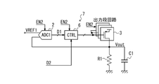
- the block diagram of the digital control regulator by one Embodiment A block diagram showing an example of a circuit configuration in an output stage circuit. The figure which shows the characteristic of a transistor in an output stage circuit. The figure which shows the fluctuation amount of the output voltage by the fluctuation of a load current.
- the block diagram which shows the 1st specific example of a digital control regulator.
- the block diagram which shows the 2nd specific example of a digital control regulator.
- the block diagram which shows the 4th specific example of a digital control regulator The block diagram which shows the 5th specific example of a digital control regulator.
- Timing diagram when capacity correction is performed only at startup A timing diagram in which the capacity correction circuit corrects the capacity according to the start of the digital LDO operation.
- Timing diagram when capacity correction is performed intermittently Timing diagram for performing capacity correction before switching the voltage level of the output voltage.
- Timing diagram when capacity correction is continuously performed before the digital LDO operation is started.
- the block diagram which shows an example of the schematic structure of the digital control regulator by this embodiment. A block diagram of a digital control regulator according to a modified example.
- FIG. 1 is a block diagram of a digital control regulator 1 according to an embodiment.
- the digital control regulator 1 of FIG. 1 is also called a digital control LDO.
- the digital control regulator 1 of FIG. 1 includes a first AD converter (hereinafter, ADC 1 or first ADC) 2, an output stage circuit 3, a replica circuit 4, and a second AD converter (hereinafter, ADC 2 or second ADC). ) 5 and a control circuit (CTRL) 6.
- ADC 1 or first ADC an AD converter
- ADC 2 or second ADC second AD converter
- CTRL control circuit
- the first ADC 2 generates a first digital signal D1 corresponding to the difference voltage between the output voltage Vout and the first reference voltage VREF1.
- the first digital signal D1 is input to the control circuit 6.
- the first ADC 2 performs an AD conversion operation when the first reference voltage VREF1 and the output voltage Vout are input.
- the output stage circuit 3 generates an output voltage Vout.
- a resistance element R1 and a capacitor C1 are connected in parallel between the output node and the ground node of the output stage circuit 3.
- the output stage circuit 3 is controlled by the control circuit 6.
- the output stage circuit 3, the first ADC 2, and the control circuit 6 constitute a digital LDO circuit 7.
- the digital LDO circuit 7 feedback controls so that the output voltage Vout matches the first reference voltage VREF1.
- the replica circuit 4 has the same circuit configuration as the output stage circuit 3 and outputs the replica voltage related to the output voltage Vout.
- the replica voltage has the same voltage level as the output voltage Vout when there is no load fluctuation.
- the replica circuit 4 and the second ADC 5 form a capability correction circuit 8 that corrects the capability of the output stage circuit 3.
- the replica circuit 4 may be enabled and output the replica voltage when the first enable signal EN1 has a predetermined logic. In this case, since the replica circuit 4 stops the output of the replica voltage when the first enable signal EN1 is other than the predetermined logic, the power consumption of the replica circuit 4 can be reduced.
- the second ADC 5 generates a second digital signal D2 according to the difference voltage between the replica voltage and the second reference voltage VREF2.
- the second digital signal D2 includes the capability information of the replica circuit 4.
- the capability information of the replica circuit 4 includes, for example, at least one information of the input voltage, the output voltage Vout, the manufacturing process, and the temperature of the replica circuit 4.
- the capability information of the replica circuit 4 is substantially the same as the capability information of the output stage circuit 3.
- the second digital signal D2 includes the on-resistance information of the replica circuit 4.
- the second ADC 5 performs an AD conversion operation when the replica voltage and the second reference voltage VREF2 are input.
- the second ADC 5 is enabled when the first enable signal EN1 has a predetermined logic, and generates the second digital signal D2.
- the second reference voltage VFEF2 is input to the second ADC 5 at the timing when the first enable signal EN1 becomes a predetermined logic. Power consumption can be reduced by limiting the period for inputting the second reference voltage VREF2 to the second ADC5 and performing the A / D conversion operation on the second ADC5 only when the first enable signal EN1 has a predetermined logic.
- the control circuit 6 generates a control signal for controlling the gain of the output stage circuit 3 based on the first digital signal D1 and the second digital signal D2.
- the control circuit 6 generates a control signal so that the output voltage Vout is not affected by the capability information of the output stage circuit 3.
- the control circuit 6 generates a control signal based on the second digital signal D2 so that the on-resistance of the output stage circuit 3 matches the on-resistance of the replica circuit 4.
- the output voltage Vout is fed back to the first ADC2, and the first digital signal D1 corresponding to the difference voltage from the first reference voltage VREF1 is generated.
- the control circuit 6 generates a control signal for controlling the gain of the output stage circuit 3 based on the first digital signal D1 and the second digital signal D2 from the second ADC 5. Since this feedback loop does not have a double loop structure, stability design can be easily performed.
- the output stage circuit 3 can adjust the on-resistance by the control signal output from the control circuit 6, and the output voltage Vout can be controlled by adjusting the on-resistance.
- the specific circuit configuration for adjusting the on-resistance in the output stage circuit 3 is arbitrary.
- the output stage circuit 3 may output the output voltage Vout when the second enable signal EN2 has a predetermined logic. Further, the second enable signal EN2 may be input to the first ADC 2 and the control circuit 6. In this case, when the second enable signal EN2 is other than the predetermined logic, the entire operation of the digital LDO circuit 7 having the first ADC2, the control circuit 6, and the output stage circuit 3 can be stopped, and the power consumption can be reduced. ..
- the output stage circuit 3 and the replica circuit 4 are, for example, circuits having the same circuit configuration including transistors of the same conductivity type and the same size.
- the output stage circuit 3 and the replica circuit 4 may be circuits having the same circuit configuration including resistance elements having the same resistance value.
- the replica circuit 4 may output the replica voltage before the output stage circuit 3 and the control circuit 6 start the feedback control of the output voltage Vout, or in synchronization with the start timing of the feedback control.
- the second ADC 5 generates the second digital signal D2 before the output stage circuit 3 and the control circuit 6 start the feedback control of the output voltage Vout, or in synchronization with the start timing of the feedback control. In this way, by correcting the capacity of the output stage circuit 3 before starting the digital LDO operation, the digital LDO operation can be performed independently of the variation in the capacity of the output stage circuit 3.
- the replica circuit 4 may output the replica voltage in synchronization with the timing at which the voltage level of the output voltage Vout is switched while the output stage circuit 3 and the control circuit 6 are performing feedback control of the output voltage Vout. good.
- the second ADC 5 generates the second digital signal D2 in synchronization with the timing at which the voltage level of the output voltage Vout is switched while the output stage circuit 3 and the control circuit 6 are performing feedback control of the output voltage Vout. do.
- the capacity correction of the output stage circuit 3 is performed again according to the timing when the voltage level of the output voltage Vout changes. By doing so, the droop characteristics, ripple characteristics, etc. can be improved.
- the replica circuit 4 may output the replica voltage a predetermined period before the timing of switching the voltage level of the output voltage Vout while the output stage circuit 3 and the control circuit 6 are performing feedback control of the output voltage Vout. good.
- the second ADC 5 generates the second digital signal D2 at the timing when the voltage level of the output voltage Vout is switched while the output stage circuit 3 and the control circuit 6 are performing feedback control of the output voltage Vout. ..
- the second digital signal including the capacity information of the replica circuit 4 is input from the second ADC 5 before the timing when the output voltage Vout is switched. It is necessary to output D2. As a result, the capacity of the output stage circuit 3 can be corrected from the timing when the output voltage Vout is switched.
- the replica circuit 4 may intermittently output the replica voltage while the output stage circuit 3 and the control circuit 6 are performing feedback control of the output voltage Vout.
- the second ADC 5 intermittently generates the second digital signal D2 while the output stage circuit 3 and the control circuit 6 are performing feedback control of the output voltage Vout.
- the replica circuit 4 may continuously output the replica voltage while the output stage circuit 3 and the control circuit 6 are performing feedback control of the output voltage Vout.
- the second ADC 5 continuously generates the second digital signal D2 while the output stage circuit 3 and the control circuit 6 are performing feedback control of the output voltage Vout.
- the replica circuit 4 may output the replica voltage when the first enable signal EN1 has a predetermined logic, and may stop the output of the replica voltage when the first enable signal EN1 has a logic other than the predetermined logic. In this way, by operating the replica circuit 4 only when necessary, the power consumption of the replica circuit 4 can be reduced.
- the second ADC 5 performs an A / D conversion operation only when the first enable signal EN1 has a predetermined logic. Further, the second reference voltage VREF2 is input to the second ADC 5 at the timing when the first enable signal EN1 becomes a predetermined logic. As a result, the power consumption of the second ADC 5 can also be reduced.
- FIG. 2 is a block diagram showing an example of the circuit configuration in the output stage circuit 3.
- a p-type MOS transistor hereinafter, simply referred to as a transistor
- the control circuit 6 outputs a control signal for controlling the number of transistors in the output stage circuit 3 to be turned on.
- the number of transistors to be turned on changes depending on the control signal, and the on-resistance of the output stage circuit 3 changes.
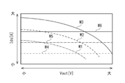
- FIG. 3A is a diagram showing the characteristics of the transistor in the output stage circuit 3.
- the horizontal axis of FIG. 3A is the output voltage Vout
- the vertical axis is the drain current of the transistor in the output stage circuit 3.
- the curves W1 to W3 in FIG. 3A show the correspondence between the output voltage Vout and the drain current when the gate-source voltage Vgs of the transistor in the output stage circuit 3 is changed in three ways (when the power supply voltage is different). Shows.
- the larger the gate-source voltage the larger the drain current and the higher the capacity of the transistor.
- FIG. 3A shows three drain current straight lines W4 to W6 having different current values.
- the order of the magnitudes of the drain currents is W4 ⁇ W5 ⁇ W6.
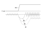
- FIG. 3B is a diagram showing the amount of fluctuation of the output voltage Vout due to the fluctuation of the load current.
- the curves W7 to W9 in FIG. 3B correspond to the straight lines W4 to W6 in FIG. 3A, respectively.
- the degree to which the output voltage Vout temporarily drops when the load current suddenly increases is called the droop characteristic.
- the smaller the Vgs, the larger the drop in the output voltage Vout, and the droop characteristic is Deteriorate.
- the higher the transistor capacity in the output stage circuit 3 the better the droop characteristics, but the circuit operation becomes unstable, the ripple voltage increases, and the noise characteristics may decrease.
- a replica circuit 4 having the same circuit configuration as the output stage circuit 3 is provided, and a second voltage corresponding to the difference voltage between the replica voltage output from the replica circuit 4 and the second reference voltage VREF2 is provided.
- the digital signal D2 is generated by the second ADC 5.
- the second digital signal D2 is a signal including the capability information of the replica circuit 4.
- the control circuit 6 controls the gain of the output stage circuit 3 based on the first digital signal D1 and the second digital signal D2 corresponding to the difference voltage between the output voltage Vout and the first reference voltage VREF1.
- control circuit 6 can control the gain of the output stage circuit 3 in consideration of the capacity information such as the input voltage, the output voltage Vout, the manufacturing process, and the temperature of the output stage circuit 3, and is originally a trade. Both the stability in the off relationship and the transient response and ripple characteristics can be improved.
- the output stage circuit 3 and the replica circuit 4 in FIG. 1 have the same circuit configuration, but various modifications can be considered for the specific circuit configurations of the output stage circuit 3 and the replica circuit 4. ..
- FIG. 4 is a block diagram showing a first specific example of the digital control regulator 1a.
- the output stage circuit 3 and the replica circuit 4 in the digital control regulator 1a of FIG. 4 have an n-type MOS transistor (hereinafter referred to as a transistor).
- the output stage circuit 3 has, for example, a plurality of transistors connected in parallel between the power supply voltage node and the output node. Although only one transistor may exist in the output stage circuit 3, an example in which a plurality of transistors are connected in parallel will be described below.
- a control signal is supplied from the control circuit 6 to the gates of the plurality of transistors in the output stage circuit 3. The on-resistance of the output stage circuit 3 is controlled by this control signal.
- the replica circuit 4 has only one transistor which is the same as the transistor connected in parallel in the output stage circuit 3.
- the replica circuit 4 outputs the replica voltage only when the first enable signal EN1 has a predetermined logic.
- the output stage circuit 3 outputs the output voltage Vout only when the second enable signal EN2 has a predetermined logic.
- the first enable signal EN1 and the second enable signal EN2 are not always indispensable, but by providing the first enable signal EN1 and the second enable signal EN2, the capability correction circuit 8 having the replica circuit 4 and the second ADC 5 and the first ADC 2 are provided. , The power consumption of the digital LDO circuit 7 having the control circuit 6 and the output stage circuit 3 can be reduced.
- the second ADC 5 has a comparator 11, a variable current source 12, and a control unit 13.
- the comparator 11 outputs a signal corresponding to the difference voltage between the replica voltage and the second reference voltage VREF2.
- the variable current source 12 controls the voltage level of the replica voltage by adjusting the current flowing through the output node of the replica circuit 4.
- the variable current source 12 is connected between the output node and the ground node in the replica circuit 4. More specifically, the variable current source 12 is connected between the source of the transistor and the grounded node in the replica circuit 4.
- the control unit 13 adjusts the current flowing through the output node to the variable current source 12 based on the output signal of the comparator 11, and turns on the replica circuit 4 for matching the replica voltage with the second reference voltage VREF2.
- a second digital signal D2 including resistance information is generated. More specifically, the control unit 13 generates an adjustment signal for adjusting the current of the variable current source 12 based on the signal output from the comparator 11. For example, if the replica voltage is lower than the second reference voltage VREF2, the control unit 13 generates an adjustment signal so as to reduce the current flowing through the variable current source 12.
- the control circuit 6 is a control signal for controlling the gain of the output stage circuit 3 based on the first digital signal D1 output from the first ADC 2 and the second digital signal D2 including the on-resistance information of the replica circuit 4. To generate.
- the on-resistance of the output stage circuit 3 can be controlled by this control signal.
- the on-resistance of the output stage circuit 3 changes depending on the capacity information such as the input voltage, output voltage Vout, manufacturing process, and temperature of the output stage circuit 3, and when the on-resistance changes, the drain current and output voltage Vout are affected. ..
- the replica circuit 4 having the same circuit configuration as the output stage circuit 3 is used, and the on-resistance information of the replica circuit 4 is detected by the second ADC 5 and supplied to the control circuit 6.
- the control circuit 6 can control the on-resistance of the output stage circuit 3 in consideration of the capability information of the output stage circuit 3.
- FIG. 5 is a block diagram showing a second specific example of the digital control regulator 1b.
- the output stage circuit 3 and the replica circuit 4 in the digital control regulator 1b of FIG. 5 have a resistance element. More specifically, it has a resistance element 4a and a switch 4b connected in series between the power supply voltage node and the output node.
- the switch 4b is for switching whether or not to use the resistance element 4a.
- a plurality of sets including a resistance element 3a and a switch 3b connected in series are connected in parallel. Any set of resistance elements 3a among a plurality of sets can be selected by the switch 3b.
- the replica circuit 4 has the same resistance element 4a and switch 4b as in the output stage circuit 3.
- the second ADC 5 has a comparator 11, a variable current source 12, and a control unit 13 as in FIG. 4.
- the variable current source 12 is connected between the output node and the ground node of the replica circuit 4.
- the control unit 13 operates in the same manner as the control unit 13 of FIG. That is, the control unit 13 adjusts the current flowing through the output node to the variable current source 12 based on the output signal of the comparator 11, and the replica circuit 4 for matching the replica voltage with the second reference voltage VREF2.
- the second digital signal D2 including the on-resistance information of is generated.
- FIG. 6 is a block diagram showing a third specific example of the digital control regulator 1c.
- the output stage circuit 3 and the replica circuit 4 in the digital control regulator 1c of FIG. 6 have a p-type MOS transistor.
- the digital control regulator 1c in FIG. 6 has different conductive types of the transistors in the output stage circuit 3 and the replica circuit 4 as compared with the digital control regulator 1a in FIG. 4, and is controlled accordingly.
- the logic of the control signal output from the circuit 6 is reversed, but the circuit operations of the digital control regulators 1a and 1c are common.
- the digital control regulator 1c of FIG. 6 is provided with a variable resistor 12a instead of the variable current source 12.
- the resistance value of the variable resistor 12a is adjusted by the adjustment signal from the control unit 13, whereby the replica voltage output from the replica circuit 4 is controlled.
- the control unit 13 in the second ADC 5 supplies the second digital signal D2 including the on-resistance information of the replica circuit 4 to the control circuit 6.
- the control circuit 6 can generate a control signal in consideration of the on-resistance information of the replica circuit 4.
- variable current source 12 is provided in the second ADC 5 and the current flowing through the variable current source 12 is controlled by the control unit 13 so that the replica voltage becomes equal to the second reference voltage VREF2.
- a constant current source that allows a constant current to flow is provided, and the number of connection stages of transistors and resistors in the output stage circuit 3 and replica circuit 4 is varied to provide information on the number of connection stages. It may be included in the second digital signal D2 as on-resistance information and supplied to the control circuit 6.
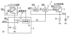
- FIG. 7 is a block diagram showing a fourth specific example of the digital control regulator 1d.
- the output stage circuit 3 and the replica circuit 4 in the digital control regulator 1d of FIG. 7 each have a plurality of p-type MO transistors (hereinafter, simply referred to as transistors) whose number of connection stages can be changed. Each transistor is connected between the power supply voltage node and the output node. As the number of connection stages of the transistors in the output stage circuit 3 and the replica circuit 4 is increased, the on-resistance of the output stage circuit 3 and the replica circuit 4 becomes smaller.
- the second ADC 5 has a comparator 11, a constant current source 12b, and a control unit 13.
- the comparator 11 outputs a signal corresponding to the difference voltage between the replica voltage and the second reference voltage VREF2.
- the constant current source 12b is connected between the output node and the ground node of the replica circuit 4, and causes a constant current to flow.
- the control unit 13 adjusts the number of connection stages of the transistors in the replica circuit 4 based on the output signal of the comparator 11, and also provides on-resistance information of the replica circuit 4 for matching the replica voltage with the second reference voltage VREF2. Generates a second digital signal D2 that includes. More specifically, the control unit 13 generates an adjustment signal so that the replica voltage matches the second reference voltage VREF2. This adjustment signal is supplied to the replica circuit 4.
- the replica circuit 4 adjusts the number of connection stages of the transistors in the replica circuit 4 based on the adjustment signal. Each transistor in the replica circuit 4 is always on, and the replica circuit 4 adjusts the number of connection stages of the transistors in the on state by the adjustment signal. For example, when the replica voltage is lower than the second reference voltage VREF2, the control unit 13 increases the number of connection stages of the transistors in the replica circuit 4. As a result, the on-resistance of the replica circuit 4 becomes smaller and the replica voltage becomes higher.
- the on-resistance of the replica circuit 4 changes depending on the number of connection stages of the transistors in the replica circuit 4.
- the control unit 13 supplies the second digital signal D2 including the on-resistance information of the replica circuit 4 to the control circuit 6.
- the control circuit 6 generates a control signal based on the first digital signal D1 and the second digital signal D2, and controls the number of connection stages of the transistors in the output stage circuit 3.
- FIG. 8 is a block diagram showing a fifth specific example of the digital control regulator 1e.
- the output stage circuit 3 and the replica circuit 4 in the digital control regulator 1e of FIG. 8 each have a plurality of n-type MOS transistors (hereinafter, simply referred to as transistors) whose number of connection stages can be changed. That is, in the digital control regulator 1e of FIGS. 7 and 8, the conductive types of the transistors in the output stage circuit 3 and the replica circuit 4 are different, and the logic of the control signal output by the control circuit 6 also changes accordingly. ..
- transistors n-type MOS transistors
- control unit 13 in the second ADC 5 supplies the second digital signal D2 including the on-resistance information of the replica circuit 4 to the control circuit 6.
- the control circuit 6 controls the number of connection stages of the transistors in the output stage circuit 3 based on the first digital signal D1 and the second digital signal D2.
- FIG. 9 is a block diagram showing a sixth specific example of the digital control regulator 1f.
- the digital control regulator 1f of FIG. 9 is provided with a plurality of resistance circuits in which the number of connection stages can be changed in the output stage circuit 3 and the replica circuit 4.
- Each resistance circuit has resistance elements 3a and 4a and switches 3b and 4b connected in series between the power supply voltage node and the output node. By turning on the switches 3b and 4b, the resistance elements 3a and 4a connected to these switches 3b and 4b can be selected. By turning on or off the switches 3b and 4b for each resistance circuit, the number of resistance elements 3a and 4a connected in parallel between the power supply voltage node and the output node can be controlled.
- the control unit 13 in the second ADC 5 supplies the second digital signal D2 including the on-resistance information of the replica circuit 4 to the control circuit 6.
- FIG. 10 is a block diagram showing a seventh specific example of the digital control regulator 1 g.
- the digital control regulator 1g of FIG. 10 has a constant current source in the digital control regulator 1d of FIG. 7 replaced with a resistance element, and other than that, it has the same circuit configuration as the digital control regulator 1d of FIG.
- the second ADC 5 transfers the on-resistance information of the replica circuit 4 to the second digital, as in the digital control regulators 1a, 1b, and 1c of FIGS. 4 to 6. It is included in the signal D2 and supplied to the control circuit 6.
- the control circuit 6 generates a control signal for controlling the gain of the output stage circuit 3 based on the first digital signal D1 and the second digital signal D2. Thereby, the output voltage Vout can be controlled in consideration of the capacity information of the output stage circuit 3.
- the replica circuit 4 and the second ADC 5 in the above-mentioned digital control regulators 1, 1a, 1b, 1c, 1d, 1e, 1f, and 1g of FIGS. 1 and 4 to 10 have a capability correction for correcting the capability of the output stage circuit 3. It constitutes a circuit 8.
- the output stage circuit 3, the first ADC 2, and the control circuit 6 constitute a digital LDO circuit.
- the digital LDO circuit performs feedback control by the first ADC 2 and the control circuit 6 so that the output voltage Vout matches the first reference voltage VREF1.
- the capacity correction circuit 8 generates the capacity information of the replica circuit 4.
- the control circuit 6 may correct the capability of the output stage circuit 3 by generating a control signal in consideration of not only the first digital signal D1 but also the second digital signal D2 output from the second ADC 5. can.
- FIG. 11 is a flowchart showing an example of a processing procedure for performing digital LDO operation and capacity correction of the output stage circuit 3.
- FIG. 11 shows a processing procedure performed by the digital control regulators 1, 1a, 1b, 1c, 1d, 1e, 1f, and 1g according to any one of FIGS. 1, 4 to 10.
- step S1 capacity correction is performed before starting the digital LDO operation (step S1).
- step S2 it is determined whether or not the capacity correction is performed only when the digital LDO operation is activated (step S3). If it is determined that the capacity correction is performed only at the time of startup, the operation of the capacity correction circuit 8 having the replica circuit 4 and the second ADC 5 is stopped (step S4), and the digital LDO operation is started (step S5).
- step S4 for example, the replica circuit 4 is disabled to prevent the replica voltage from being output from the replica circuit 4. Alternatively, the supply of the power supply voltage to the replica circuit 4 and the second ADC 5 may be cut off. As a result, the power consumption in the replica circuit 4 and the second ADC 5 can be suppressed.
- step S6 it is determined whether or not to perform capacity correction intermittently.
- step S6 it is determined whether or not to perform capacity correction intermittently.
- step S6 it is determined whether or not the capacity correction is performed intermittently, the operation of the capacity correction circuit 8 is stopped (step S7), and the digital LDO operation is started (step S8).
- step S9 it is determined whether or not the timing for intermittently performing capacity correction has been reached again (step S9), and when the timing for performing capacity correction comes, the capacity correction circuit 8 is operated (step S10), and the second ADC 5 to the second ADC 5 are performed. 2
- the digital signal D2 is output (step S11).
- step S11 the second digital signal D2 is updated every time the capability is corrected intermittently.
- step S7 and subsequent steps are repeated. If NO is determined in step S6, the capacity correction is continuously performed during the digital LDO operation (steps S12 and S13).
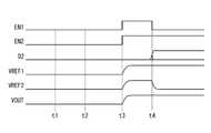
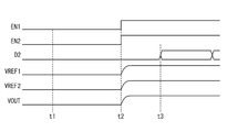
- FIG. 12 is a timing diagram in the case of YES in step S3 of FIG. 11, that is, the case where the ability correction is performed only at the time of activation.
- the first enable signal EN1 of the capability correction circuit 8 having the replica circuit 4 and the second ADC5 and the second enable signal EN2 of the digital LDO circuit 7 having the first ADC2, the control unit 13 circuit, and the output stage circuit 3 are shown.
- the signal waveforms of the second digital signal D2, the first reference voltage VREF1, the second reference voltage VREF2, and the output voltage Vout are shown.
- the time t1 to t3 in FIG. 12 is before the start of the digital LDO operation, and the first enable signal EN1 input to the replica circuit 4 becomes high within the period from time t1 to t2.
- the capacity correction circuit 8 having the replica circuit 4 and the second ADC 5 performs the capacity correction process.
- the second reference voltage VREF2 is input to the second ADC 5 within the period from time t1 to t2.
- the second ADC 5 outputs the second digital signal D2 including the on-resistance information of the replica circuit 4 at time t2.
- the replica circuit 4 is disabled at time t2, and the second reference voltage VREF2 is not input to the second ADC 5, but the second ADC 5 holds the second digital signal D2 output at time t2.
- the control circuit 6 After that, the first reference voltage VREF1 is input to the first ADC2 during the period after the time t3, and the digital LDO operation is performed. At this time, the control circuit 6 generates a control signal based on the first digital signal D1 and the second digital signal D2. This control signal is a signal in which the capability correction of the output stage circuit 3 is added to the digital LDO operation. As a result, the output stage circuit 3 outputs the output voltage Vout with the capacity corrected of the output stage circuit 3.
- the timing at which the capacity correction circuit 8 having the replica circuit 4 and the second ADC 5 performs the capacity correction may not be before the digital LDO operation is performed, but may be a timing that coincides with the start of the digital LDO operation.
- FIG. 13 is a timing diagram in which the capacity correction circuit 8 performs capacity correction in accordance with the start of the digital LDO operation.
- the first enable signal EN1 of the replica circuit 4 becomes high, and the second reference voltage VREF2 is input to the second ADC5. Therefore, after the time t3, the output voltage Vout in which the digital LDO operation is performed is output. Further, at time t4, the second ADC 5 outputs a second digital signal D2 including the on-resistance information of the replica circuit 4.
- the control signal including the capacity correction of the output stage circuit 3 is output from the control unit 13. Therefore, the output stage circuit 3 outputs the output voltage Vout after the capacity correction of the output stage circuit 3 is performed after the time t4.
- the above-mentioned digital control regulators 1 to 1 g may intermittently perform capacity correction by the capacity correction circuit 8.
- FIG. 14 is a timing diagram when capacity correction is performed intermittently.
- the capacity correction circuit 8 corrects the capacity of the output stage circuit 3 during the period from time t1 to t2 before the digital LDO operation is started and the time t4 to t5 after the digital LDO operation is started. Although omitted in FIG. 14, the capability correction circuit 8 intermittently performs capability correction during the digital LDO operation period even after the time t5.
- FIG. 14 shows an example in which the output stage circuit 3 switches the voltage level of the output voltage Vout at time t4, and the capacity correction circuit 8 performs capacity correction according to the timing at which the voltage level of the output voltage Vout is switched. This is because when the output voltage Vout of the output stage circuit 3 changes, the droop characteristics, ripple characteristics, and the like change.
- the first enable signal EN1 of the replica circuit 4 becomes high and becomes the enable state within the period from the time t4 to t5.
- the second reference voltage VREF2 is input to the second ADC 5 within the period from time t4 to t5.
- the second ADC 5 outputs the second digital signal D2 including the capability information of the replica circuit 4 at time t5, and after the time t5, the output stage circuit 3 outputs the output voltage Vout including the capability correction of the output stage circuit 3. do.
- capacity correction may be performed at regular time intervals, and as shown at time t4 in FIG. 14, after the digital LDO operation is started, the output voltage Vout of the output stage circuit 3
- the capacity correction may be performed only when the voltage level changes.
- the capacity is corrected when the voltage level of the output voltage Vout is switched, but as shown in the timing diagram of FIG. 15, the capacity is corrected prior to the timing of switching the voltage level of the output voltage Vout. You may.
- the capacity is corrected within the period from time t1 to t2 before the digital LDO operation is disclosed, and the time t4 immediately before the time t5 when the voltage level of the output voltage Vout is switched after the digital LDO operation is started.
- An example of performing capacity correction within the period of ⁇ t5 is shown.
- the digital control regulators 1 to 1 g know the timing of switching the voltage level of the output voltage Vout, it is possible to perform the capacity correction within the period of time t4 to t5 immediately before switching the voltage level of the output voltage Vout. be.
- the second digital signal D2 including the capability information of the replica circuit 4 can be output from the second ADC 5. Therefore, after the time t5 when the voltage level of the output voltage Vout is switched, the output voltage Vout corrected for the capacity of the output stage circuit 3 can be output. That is, when switching the voltage level of the output voltage Vout, the output voltage Vout with the capacity corrected can be output from the time of switching.
- the above-mentioned digital control regulators 1 to 1 g may continuously perform capacity correction by the capacity correction circuit 8.
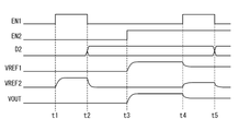
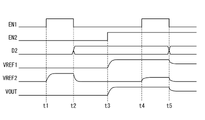
- 16 and 17 are timing diagrams in the case of continuous capacity correction.
- FIG. 16 shows a timing diagram when capacity correction is continuously performed before the digital LDO operation is started.
- FIG. 17 shows an example in which the capacity correction is continuously performed according to the timing at which the digital LDO operation is started.
- the first enable signal EN1 input to the replica circuit 4 becomes high and is in the enable state.
- the first enable signal EN1 maintains a high level after time t1.
- the second reference voltage VREF2 is continuously input to the second ADC5.
- the second ADC 5 outputs a second digital signal D2 including the capability information of the replica circuit 4. Since the second ADC 5 continues to operate after the time t2, the second digital signal D2 is updated at any time according to the capability information of the replica circuit 4.
- the second enable signal EN2 input to the output stage circuit 3 becomes high and becomes an enable state. Further, after the time t3, the first reference voltage VREF1 is continuously input to the first ADC2.
- the control circuit 6 generates a control signal based on the first digital signal D1 output from the first ADC 2 and the second digital signal D2 output from the second ADC 5.
- the output stage circuit 3 outputs the output voltage Vout to which the capacity correction of the output stage circuit 3 is added based on the control signal after the time t3.
- the first enable signal EN1 input to the replica circuit 4 and the second enable signal EN2 input to the output stage circuit 3 are both high, and the replica circuit 4 and the output stage circuit 3 are set to high. It will continue to be enabled after time t2.
- the first reference voltage VREF1 is input to the first ADC2
- the second reference voltage VREF2 is input to the second ADC5.
- the first reference voltage VREF1 and the second reference voltage VREF2 are continuously input to the first ADC2 and the second ADC5 after the time t2, respectively.
- the second ADC 5 outputs the second digital signal D2 including the on-resistance information of the replica circuit 4 after the time t3.
- the second digital signal D2 is continuously updated after the time t3 based on the latest on-resistance information of the replica circuit 4.
- the output stage circuit 3 continuously outputs the output voltage Vout in consideration of the capacity correction of the output stage circuit 3 after the time t3.
- the output voltage Vout output from the output stage circuit 3, the first reference voltage VREF1 input to the first ADC2, and the second reference voltage VREF2 input to the second ADC5 have related voltage levels, respectively. ..
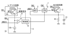
- FIG. 18 is a block diagram showing an example of a schematic configuration of the digital control regulator 1h according to the present embodiment.
- the digital control regulator 1h of FIG. 18 has a configuration in which the digital control regulator 1 of FIG. 1 is more embodied.
- the same components as those in FIG. 1 are designated by the same reference numerals, and the differences will be mainly described below.
- the digital control regulator 1h of FIG. 18 includes a first reference voltage generation circuit 14 that generates a first reference voltage VREF1 and a second reference voltage generation circuit 15 that generates a second reference voltage VREF2.
- a variable load circuit 16 is provided.
- the first reference voltage generation circuit 14 has a first current source 17 and a first variable resistor 18 connected in series between a power supply voltage node and a ground node.
- the second reference voltage generation circuit 15 has a second current source 19 and a second variable resistor 20 connected in series between the power supply voltage node and the ground node.
- variable load circuit 16 is connected between the output node and the ground node of the replica circuit 4, and the resistance value is variably controlled by the adjustment signal from the second ADC 5.
- a specific example of the variable load circuit 16 is the variable current source 12 and the variable resistor shown in FIGS. 4 to 6.
- the control circuit 6 performs feedback control so that the output voltage Vout matches the first reference voltage VREF1.
- FIG. 19 is a block diagram of a digital control regulator 1i according to a modified example.
- FIG. 19 includes a resistance voltage divider circuit 21 and a voltage amplifier 22 in addition to the circuit configuration of FIG.
- the resistance voltage dividing circuit 21 is connected between the output node and the ground node of the output stage circuit 3 and divides the output voltage Vout.
- the voltage divided voltage divided by the resistance voltage dividing circuit 21 is input to the first ADC 2.
- the resistance voltage divider circuit 21 generates a voltage divider voltage obtained by multiplying the output voltage Vout by 1 / A.
- the first ADC 2 generates a first digital signal D1 corresponding to the difference voltage between the voltage dividing voltage and the first reference voltage VREF1.
- the feedback control is performed so that the divided voltage becomes the same as the first reference voltage VREF1, the voltage level of the first reference voltage VREF1 can be lowered.
- the replica circuit 4 outputs a replica voltage having a voltage level similar to that of the output stage circuit 3.
- the second reference voltage VREF2 is set to the same voltage level as the first reference voltage VREF1. Therefore, the second reference voltage VREF2 is multiplied by A by the voltage amplifier 22 to be about the same as the voltage level of the replica voltage.
- the replica circuit 4 having the same circuit configuration as the output stage circuit 3 is provided, and the second digital signal D2 including the capability information of the replica circuit 4 is supplied to the control circuit 6, so that the control circuit 6 is used.
- the fluctuation of the ripple voltage and the fluctuation of the droop characteristic can be suppressed.
- the present embodiment since the influence of the capacity variation of the output stage circuit 3 is reduced, it is not necessary to complicate the circuit configuration inside the digital control regulators 1 to 1i, and the stability can be improved. More specifically, the present embodiment does not require a multiple loop configuration for digital LDO operation, which facilitates control and improves stability.
- a circuit having a low voltage and a small area can be configured, and integration is easy, so that the manufacturing cost can be reduced.
- the present technology can have the following configurations.
- a first AD converter that generates a first digital signal according to the difference voltage between the output voltage and the first reference voltage, and The output stage circuit that generates the output voltage and A replica circuit having the same circuit configuration as the output stage circuit and outputting a replica voltage related to the output voltage
- a second AD converter that generates a second digital signal according to the difference voltage between the replica voltage and the second reference voltage
- a digital control regulator comprising a control circuit for generating a control signal for controlling a gain of the output stage circuit based on the first digital signal and the second digital signal.
- the digital control regulator according to (1), wherein the output stage circuit and the replica circuit are circuits having the same circuit configuration including resistance elements having the same resistance value.
- the second digital signal includes capability information of the replica circuit.
- the control circuit generates the control signal so that the output voltage is not affected by the capability information of the output stage circuit.
- the capability information includes at least one information of an input voltage, an output voltage, a manufacturing process, and a temperature of the replica circuit or the output stage circuit.
- the second digital signal includes on-resistance information of the replica circuit.
- Control regulator. (9)
- the replica circuit outputs the replica voltage before the output stage circuit and the control circuit start the feedback control of the output voltage, or in synchronization with the start timing of the feedback control.
- the second AD converter generates the second digital signal before the output stage circuit and the control circuit start the feedback control of the output voltage, or in synchronization with the start timing of the feedback control.
- the digital control regulator according to any one of 1) to (8).
- the replica circuit outputs the replica voltage in synchronization with the timing at which the voltage level of the output voltage is switched while the output stage circuit and the control circuit are performing feedback control of the output voltage.
- the second AD converter synchronizes with the timing at which the voltage level of the output voltage is switched while the output stage circuit and the control circuit are performing feedback control of the output voltage, and the second digital signal.
- the digital control regulator according to (9).
- (11) The replica circuit outputs the replica voltage a predetermined period before the timing of switching the voltage level of the output voltage while the output stage circuit and the control circuit are performing feedback control of the output voltage.
- the second AD converter outputs the second digital signal at the timing when the voltage level of the output voltage is switched while the output stage circuit and the control circuit are performing feedback control of the output voltage.
- the digital control regulator according to (9) or (10) to be generated.
- the replica circuit intermittently outputs the replica voltage while the output stage circuit and the control circuit are performing feedback control of the output voltage.
- the second AD converter intermittently generates the second digital signal while the output stage circuit and the control circuit are performing feedback control of the output voltage, (1) to (8).
- the digital control regulator according to any one of the above.
- the replica circuit continuously outputs the replica voltage while the output stage circuit and the control circuit are performing feedback control of the output voltage.
- the second AD converter continuously generates the second digital signal while the output stage circuit and the control circuit are performing feedback control of the output voltage, (1) to (8).
- the digital control regulator according to any one of the above.
- the replica circuit outputs the replica voltage when the enable signal has a predetermined logic, and stops the output of the replica voltage when the enable signal has a logic other than the predetermined logic, (9) to The digital control regulator according to any one of (13).
- the second AD converter is A comparator that outputs a signal corresponding to the difference voltage between the replica voltage and the second reference voltage, and A variable load circuit that controls the voltage level of the replica voltage by adjusting the current flowing through the output node of the replica circuit.
- the digital control regulator according to any one of (1) to (15), comprising a control unit for generating the second digital signal including the second digital signal. (17) In the replica circuit, the number of connection stages of a transistor or a resistance element can be adjusted.
- the second AD converter is A comparator that outputs a signal corresponding to the difference voltage between the replica voltage and the second reference voltage, and Based on the output signal of the comparator, the number of connection stages of the transistor or the resistance element in the replica circuit is adjusted, and the on-resistance information of the replica circuit for matching the replica voltage with the second reference voltage is included.
- the digital control regulator according to any one of (1) to (15), comprising a control unit for generating the second digital signal. (18) In the output stage circuit, the number of connection stages of a transistor or a resistance element can be adjusted.
- the control circuit Based on the second digital signal, the control circuit makes the number of connection stages of transistors or resistance elements in the output stage circuit the same as the number of connection stages of transistors or resistance elements in the replica circuit, (1) to The digital control regulator according to any one of (17).
- the control circuit feedback controls so that the output voltage becomes equal to the first reference voltage.
- the control circuit feedback-controls the output voltage so that the voltage divided by 1 / A (A is a real number larger than 1) times equal to the first reference voltage.
- the second reference voltage is set to the same voltage level as the first reference voltage.
- the digital control regulator according to any one of (1) to (18), wherein the second AD converter compares the replica voltage with a voltage obtained by multiplying the second reference voltage by A.
Landscapes
- Engineering & Computer Science (AREA)
- Theoretical Computer Science (AREA)
- Physics & Mathematics (AREA)
- Electromagnetism (AREA)
- General Physics & Mathematics (AREA)
- Radar, Positioning & Navigation (AREA)
- Automation & Control Theory (AREA)
- Continuous-Control Power Sources That Use Transistors (AREA)
Abstract
Description
前記出力電圧を生成する出力段回路と、
前記出力段回路と同じ回路構成を有し、前記出力電圧に関連するレプリカ電圧を出力するレプリカ回路と、
前記レプリカ電圧と第2基準電圧との差分電圧に応じた第2デジタル信号を生成する第2のAD変換器と、
前記第1デジタル信号及び前記第2デジタル信号に基づいて、前記出力段回路のゲインを制御する制御信号を生成する制御回路と、を備える、デジタル制御レギュレータが提供される。
前記第2のAD変換器は、前記出力段回路及び前記制御回路が前記出力電圧の帰還制御を開始する前、又は前記帰還制御の開始タイミングに同期させて前記第2デジタル信号を生成してもよい。
前記第2のAD変換器は、前記出力段回路及び前記制御回路が前記出力電圧の帰還制御を行っている最中に前記出力電圧の電圧レベルを切り替えたタイミングに同期させて前記第2デジタル信号を生成してもよい。
前記第2のAD変換器は、前記出力段回路及び前記制御回路が前記出力電圧の帰還制御を行っている最中に前記出力電圧の電圧レベルを切り替えたタイミングに合わせて前記第2デジタル信号を生成してもよい。
前記第2のAD変換器は、前記出力段回路及び前記制御回路が前記出力電圧の帰還制御を行っている最中に間欠的に前記第2デジタル信号を生成してもよい。
前記第2のAD変換器は、前記出力段回路及び前記制御回路が前記出力電圧の帰還制御を行っている最中に継続して前記第2デジタル信号を生成してもよい。
前記レプリカ電圧と前記第2基準電圧との差分電圧に応じた信号を出力する比較器と、
前記レプリカ回路の出力ノードに流れる電流を調整することにより、前記レプリカ電圧の電圧レベルを制御する可変負荷回路と、
前記比較器の出力信号に基づいて、前記出力ノードを通って前記可変負荷回路に流れる電流を調整するとともに、前記レプリカ電圧を前記第2基準電圧に一致させるための前記レプリカ回路のオン抵抗情報を含む前記第2デジタル信号を生成する制御部と、を有してもよい。
前記第2のAD変換器は、
前記レプリカ電圧と前記第2基準電圧との差分電圧に応じた信号を出力する比較器と、
前記比較器の出力信号に基づいて、前記レプリカ回路内のトランジスタ又は抵抗素子の接続段数を調整するとともに、前記レプリカ電圧を前記第2基準電圧に一致させるための前記レプリカ回路のオン抵抗情報を含む前記第2デジタル信号を生成する制御部と、を有してもよい。
前記制御回路は、前記第2デジタル信号に基づいて、前記出力段回路内のトランジスタ又は抵抗素子の接続段数を、前記レプリカ回路内のトランジスタ又は抵抗素子の接続段数と同一にしてもよい。
前記第1基準電圧と前記第2基準電圧とは、同一の電圧レベルであってもよい。
前記第2基準電圧は、前記第1基準電圧と同一の電圧レベルに設定され、
前記第2のAD変換器は、前記レプリカ電圧と前記第2基準電圧をA倍した電圧とを比較してもよい。
(1)出力電圧と第1基準電圧との差分電圧に応じた第1デジタル信号を生成する第1のAD変換器と、
前記出力電圧を生成する出力段回路と、
前記出力段回路と同じ回路構成を有し、前記出力電圧に関連するレプリカ電圧を出力するレプリカ回路と、
前記レプリカ電圧と第2基準電圧との差分電圧に応じた第2デジタル信号を生成する第2のAD変換器と、
前記第1デジタル信号及び前記第2デジタル信号に基づいて、前記出力段回路のゲインを制御する制御信号を生成する制御回路と、を備える、デジタル制御レギュレータ。
(2)前記出力段回路及び前記レプリカ回路は、同一導電型かつ同一サイズのトランジスタを含む同一回路構成の回路である、(1)に記載のデジタル制御レギュレータ。
(3)前記出力段回路及び前記レプリカ回路は、同一抵抗値の抵抗素子を含む同一回路構成の回路である、(1)に記載のデジタル制御レギュレータ。
(4)前記第2デジタル信号は、前記レプリカ回路の能力情報を含む、(1)乃至(3)のいずれか一項に記載のデジタル制御レギュレータ。
(5)前記制御回路は、前記出力電圧が前記出力段回路の能力情報による変動を受けないように、前記制御信号を生成する、(4)に記載のデジタル制御レギュレータ。
(6)前記能力情報は、前記レプリカ回路又は前記出力段回路の入力電圧、出力電圧、製造プロセス、及び温度の少なくとも一つの情報を含む、(4)又は(5)に記載のデジタル制御レギュレータ。
(7)前記第2デジタル信号は、前記レプリカ回路のオン抵抗情報を含む、(1)乃至(6)のいずれか一項に記載のデジタル制御レギュレータ。
(8)前記制御回路は、前記第2デジタル信号に基づいて、前記出力段回路のオン抵抗が前記レプリカ回路のオン抵抗に一致するように前記制御信号を生成する、(7)に記載のデジタル制御レギュレータ。
(9)前記レプリカ回路は、前記出力段回路及び前記制御回路が前記出力電圧の帰還制御を開始する前、又は前記帰還制御の開始タイミングに同期させて前記レプリカ電圧を出力し、
前記第2のAD変換器は、前記出力段回路及び前記制御回路が前記出力電圧の帰還制御を開始する前、又は前記帰還制御の開始タイミングに同期させて前記第2デジタル信号を生成する、(1)乃至(8)のいずれか一項に記載のデジタル制御レギュレータ。
(10)前記レプリカ回路は、前記出力段回路及び前記制御回路が前記出力電圧の帰還制御を行っている最中に前記出力電圧の電圧レベルを切り替えたタイミングに同期させて前記レプリカ電圧を出力し、
前記第2のAD変換器は、前記出力段回路及び前記制御回路が前記出力電圧の帰還制御を行っている最中に前記出力電圧の電圧レベルを切り替えたタイミングに同期させて前記第2デジタル信号を生成する、(9)に記載のデジタル制御レギュレータ。
(11)前記レプリカ回路は、前記出力段回路及び前記制御回路が前記出力電圧の帰還制御を行っている最中に前記出力電圧の電圧レベルを切り替えるタイミングより所定期間前に前記レプリカ電圧を出力し、
前記第2のAD変換器は、前記出力段回路及び前記制御回路が前記出力電圧の帰還制御を行っている最中に前記出力電圧の電圧レベルを切り替えたタイミングに合わせて前記第2デジタル信号を生成する、(9)又は(10)に記載のデジタル制御レギュレータ。
(12)前記レプリカ回路は、前記出力段回路及び前記制御回路が前記出力電圧の帰還制御を行っている最中に間欠的に前記レプリカ電圧を出力し、
前記第2のAD変換器は、前記出力段回路及び前記制御回路が前記出力電圧の帰還制御を行っている最中に間欠的に前記第2デジタル信号を生成する、(1)乃至(8)のいずれか一項に記載のデジタル制御レギュレータ。
(13)前記レプリカ回路は、前記出力段回路及び前記制御回路が前記出力電圧の帰還制御を行っている最中に継続して前記レプリカ電圧を出力し、
前記第2のAD変換器は、前記出力段回路及び前記制御回路が前記出力電圧の帰還制御を行っている最中に継続して前記第2デジタル信号を生成する、(1)乃至(8)のいずれか一項に記載のデジタル制御レギュレータ。
(14)前記レプリカ回路は、イネーブル信号が所定の論理のときに前記レプリカ電圧を出力し、前記イネーブル信号が前記所定の論理以外の論理のときには前記レプリカ電圧の出力を停止する、(9)乃至(13)のいずれか一項に記載のデジタル制御レギュレータ。
(15)前記イネーブル信号が前記所定の論理になるタイミングに合わせて、前記第2基準電圧が前記第2のAD変換器に入力される、(14)に記載のデジタル制御レギュレータ。
(16)前記第2のAD変換器は、
前記レプリカ電圧と前記第2基準電圧との差分電圧に応じた信号を出力する比較器と、
前記レプリカ回路の出力ノードに流れる電流を調整することにより、前記レプリカ電圧の電圧レベルを制御する可変負荷回路と、
前記比較器の出力信号に基づいて、前記出力ノードを通って前記可変負荷回路に流れる電流を調整するとともに、前記レプリカ電圧を前記第2基準電圧に一致させるための前記レプリカ回路のオン抵抗情報を含む前記第2デジタル信号を生成する制御部と、を有する、(1)乃至(15)のいずれか一項に記載のデジタル制御レギュレータ。
(17)前記レプリカ回路は、トランジスタ又は抵抗素子の接続段数を調整可能であり、
前記第2のAD変換器は、
前記レプリカ電圧と前記第2基準電圧との差分電圧に応じた信号を出力する比較器と、
前記比較器の出力信号に基づいて、前記レプリカ回路内のトランジスタ又は抵抗素子の接続段数を調整するとともに、前記レプリカ電圧を前記第2基準電圧に一致させるための前記レプリカ回路のオン抵抗情報を含む前記第2デジタル信号を生成する制御部と、を有する、(1)乃至(15)のいずれか一項に記載のデジタル制御レギュレータ。
(18)前記出力段回路は、トランジスタ又は抵抗素子の接続段数を調整可能であり、
前記制御回路は、前記第2デジタル信号に基づいて、前記出力段回路内のトランジスタ又は抵抗素子の接続段数を、前記レプリカ回路内のトランジスタ又は抵抗素子の接続段数と同一にする、(1)乃至(17)のいずれか一項に記載のデジタル制御レギュレータ。
(19)前記制御回路は、前記出力電圧が前記第1基準電圧と等しくなるように帰還制御し、
前記第1基準電圧と前記第2基準電圧とは、同一の電圧レベルである、(1)乃至(18)のいずれか一項に記載のデジタル制御レギュレータ。
(20)前記制御回路は、前記出力電圧を1/A(Aは1より大きい実数)倍に分圧した電圧が前記第1基準電圧と等しくなるように帰還制御し、
前記第2基準電圧は、前記第1基準電圧と同一の電圧レベルに設定され、
前記第2のAD変換器は、前記レプリカ電圧と前記第2基準電圧をA倍した電圧とを比較する、(1)乃至(18)のいずれか一項に記載のデジタル制御レギュレータ。
Claims (20)
- 出力電圧と第1基準電圧との差分電圧に応じた第1デジタル信号を生成する第1のAD変換器と、
前記出力電圧を生成する出力段回路と、
前記出力段回路と同じ回路構成を有し、前記出力電圧に関連するレプリカ電圧を出力するレプリカ回路と、
前記レプリカ電圧と第2基準電圧との差分電圧に応じた第2デジタル信号を生成する第2のAD変換器と、
前記第1デジタル信号及び前記第2デジタル信号に基づいて、前記出力段回路のゲインを制御する制御信号を生成する制御回路と、を備える、デジタル制御レギュレータ。 - 前記出力段回路及び前記レプリカ回路は、同一導電型かつ同一サイズのトランジスタを含む同一回路構成の回路である、請求項1に記載のデジタル制御レギュレータ。
- 前記出力段回路及び前記レプリカ回路は、同一抵抗値の抵抗素子を含む同一回路構成の回路である、請求項1に記載のデジタル制御レギュレータ。
- 前記第2デジタル信号は、前記レプリカ回路の能力情報を含む、請求項1に記載のデジタル制御レギュレータ。
- 前記制御回路は、前記出力電圧が前記出力段回路の能力情報による変動を受けないように、前記制御信号を生成する、請求項4に記載のデジタル制御レギュレータ。
- 前記能力情報は、前記レプリカ回路又は前記出力段回路の入力電圧、出力電圧、製造プロセス、及び温度の少なくとも一つの情報を含む、請求項4に記載のデジタル制御レギュレータ。
- 前記第2デジタル信号は、前記レプリカ回路のオン抵抗情報を含む、請求項1に記載のデジタル制御レギュレータ。
- 前記制御回路は、前記第2デジタル信号に基づいて、前記出力段回路のオン抵抗が前記レプリカ回路のオン抵抗に一致するように前記制御信号を生成する、請求項7に記載のデジタル制御レギュレータ。
- 前記レプリカ回路は、前記出力段回路及び前記制御回路が前記出力電圧の帰還制御を開始する前、又は前記帰還制御の開始タイミングに同期させて前記レプリカ電圧を出力し、
前記第2のAD変換器は、前記出力段回路及び前記制御回路が前記出力電圧の帰還制御を開始する前、又は前記帰還制御の開始タイミングに同期させて前記第2デジタル信号を生成する、請求項1に記載のデジタル制御レギュレータ。 - 前記レプリカ回路は、前記出力段回路及び前記制御回路が前記出力電圧の帰還制御を行っている最中に前記出力電圧の電圧レベルを切り替えたタイミングに同期させて前記レプリカ電圧を出力し、
前記第2のAD変換器は、前記出力段回路及び前記制御回路が前記出力電圧の帰還制御を行っている最中に前記出力電圧の電圧レベルを切り替えたタイミングに同期させて前記第2デジタル信号を生成する、請求項9に記載のデジタル制御レギュレータ。 - 前記レプリカ回路は、前記出力段回路及び前記制御回路が前記出力電圧の帰還制御を行っている最中に前記出力電圧の電圧レベルを切り替えるタイミングより所定期間前に前記レプリカ電圧を出力し、
前記第2のAD変換器は、前記出力段回路及び前記制御回路が前記出力電圧の帰還制御を行っている最中に前記出力電圧の電圧レベルを切り替えたタイミングに合わせて前記第2デジタル信号を生成する、請求項9に記載のデジタル制御レギュレータ。 - 前記レプリカ回路は、前記出力段回路及び前記制御回路が前記出力電圧の帰還制御を行っている最中に間欠的に前記レプリカ電圧を出力し、
前記第2のAD変換器は、前記出力段回路及び前記制御回路が前記出力電圧の帰還制御を行っている最中に間欠的に前記第2デジタル信号を生成する、請求項1に記載のデジタル制御レギュレータ。 - 前記レプリカ回路は、前記出力段回路及び前記制御回路が前記出力電圧の帰還制御を行っている最中に継続して前記レプリカ電圧を出力し、
前記第2のAD変換器は、前記出力段回路及び前記制御回路が前記出力電圧の帰還制御を行っている最中に継続して前記第2デジタル信号を生成する、請求項1に記載のデジタル制御レギュレータ。 - 前記レプリカ回路は、イネーブル信号が所定の論理のときに前記レプリカ電圧を出力し、前記イネーブル信号が前記所定の論理以外の論理のときには前記レプリカ電圧の出力を停止する、請求項9に記載のデジタル制御レギュレータ。
- 前記イネーブル信号が前記所定の論理になるタイミングに合わせて、前記第2基準電圧が前記第2のAD変換器に入力される、請求項14に記載のデジタル制御レギュレータ。
- 前記第2のAD変換器は、
前記レプリカ電圧と前記第2基準電圧との差分電圧に応じた信号を出力する比較器と、
前記レプリカ回路の出力ノードに流れる電流を調整することにより、前記レプリカ電圧の電圧レベルを制御する可変負荷回路と、
前記比較器の出力信号に基づいて、前記出力ノードを通って前記可変負荷回路に流れる電流を調整するとともに、前記レプリカ電圧を前記第2基準電圧に一致させるための前記レプリカ回路のオン抵抗情報を含む前記第2デジタル信号を生成する制御部と、を有する、請求項1に記載のデジタル制御レギュレータ。 - 前記レプリカ回路は、トランジスタ又は抵抗素子の接続段数を調整可能であり、
前記第2のAD変換器は、
前記レプリカ電圧と前記第2基準電圧との差分電圧に応じた信号を出力する比較器と、
前記比較器の出力信号に基づいて、前記レプリカ回路内のトランジスタ又は抵抗素子の接続段数を調整するとともに、前記レプリカ電圧を前記第2基準電圧に一致させるための前記レプリカ回路のオン抵抗情報を含む前記第2デジタル信号を生成する制御部と、を有する、請求項1に記載のデジタル制御レギュレータ。 - 前記出力段回路は、トランジスタ又は抵抗素子の接続段数を調整可能であり、
前記制御回路は、前記第2デジタル信号に基づいて、前記出力段回路内のトランジスタ又は抵抗素子の接続段数を、前記レプリカ回路内のトランジスタ又は抵抗素子の接続段数と同一にする、請求項1に記載のデジタル制御レギュレータ。 - 前記制御回路は、前記出力電圧が前記第1基準電圧と等しくなるように帰還制御し、
前記第1基準電圧と前記第2基準電圧とは、同一の電圧レベルである、請求項1に記載のデジタル制御レギュレータ。 - 前記制御回路は、前記出力電圧を1/A(Aは1より大きい実数)倍に分圧した電圧が前記第1基準電圧と等しくなるように帰還制御し、
前記第2基準電圧は、前記第1基準電圧と同一の電圧レベルに設定され、
前記第2のAD変換器は、前記レプリカ電圧と前記第2基準電圧をA倍した電圧とを比較する、請求項1に記載のデジタル制御レギュレータ。
Priority Applications (2)
| Application Number | Priority Date | Filing Date | Title |
|---|---|---|---|
| JP2022553951A JP7744917B2 (ja) | 2020-09-30 | 2021-09-27 | デジタル制御レギュレータ |
| US18/245,870 US12407361B2 (en) | 2020-09-30 | 2021-09-27 | Digital control regulator |
Applications Claiming Priority (2)
| Application Number | Priority Date | Filing Date | Title |
|---|---|---|---|
| JP2020-165473 | 2020-09-30 | ||
| JP2020165473 | 2020-09-30 |
Publications (1)
| Publication Number | Publication Date |
|---|---|
| WO2022071222A1 true WO2022071222A1 (ja) | 2022-04-07 |
Family
ID=80951636
Family Applications (1)
| Application Number | Title | Priority Date | Filing Date |
|---|---|---|---|
| PCT/JP2021/035375 Ceased WO2022071222A1 (ja) | 2020-09-30 | 2021-09-27 | デジタル制御レギュレータ |
Country Status (3)
| Country | Link |
|---|---|
| US (1) | US12407361B2 (ja) |
| JP (1) | JP7744917B2 (ja) |
| WO (1) | WO2022071222A1 (ja) |
Cited By (1)
| Publication number | Priority date | Publication date | Assignee | Title |
|---|---|---|---|---|
| EP4439226A1 (en) * | 2023-03-29 | 2024-10-02 | INTEL Corporation | A bias-less technique for design of a digital linear voltage regulator |
Citations (2)
| Publication number | Priority date | Publication date | Assignee | Title |
|---|---|---|---|---|
| JP2013225306A (ja) * | 2012-04-23 | 2013-10-31 | Samsung Electro-Mechanics Co Ltd | 位相マージン補償手段を有するldo及びそれを用いた位相マージン補償方法 |
| JP2020516978A (ja) * | 2017-04-11 | 2020-06-11 | インテル コーポレイション | 線形及び非線形制御メカニズムを含む適応デジタルコントローラ |
Family Cites Families (12)
| Publication number | Priority date | Publication date | Assignee | Title |
|---|---|---|---|---|
| US7521913B2 (en) * | 2004-09-10 | 2009-04-21 | Primarion Corporation | Active transient response circuits, system and method for digital multiphase pulse width modulated regulators |
| US8305061B1 (en) * | 2008-06-04 | 2012-11-06 | National Semiconductor Corporation | Apparatus and method for digitally controlled buck-boost switching regulator |
| US7619402B1 (en) * | 2008-09-26 | 2009-11-17 | Hong Kong Applied Science And Technology Research Institute Co., Ltd. | Low dropout voltage regulator with programmable on-chip output voltage for mixed signal embedded applications |
| US9417643B2 (en) | 2013-03-15 | 2016-08-16 | Qualcomm Incorporated | Voltage regulator with variable impedance element |
| US9841775B2 (en) * | 2014-12-11 | 2017-12-12 | Honeywell International Inc. | Systems and methods for ultra-precision regulated voltage |
| US10216209B1 (en) * | 2018-06-11 | 2019-02-26 | SK Hynix Inc. | Digital low drop-out regulator and operation method thereof |
| JP2020201730A (ja) * | 2019-06-11 | 2020-12-17 | ソニーセミコンダクタソリューションズ株式会社 | デジタル制御低ドロップアウトレギュレータ |
| TWI753548B (zh) * | 2020-08-26 | 2022-01-21 | 華邦電子股份有限公司 | 低壓差穩壓器 |
| KR20220044019A (ko) * | 2020-09-29 | 2022-04-06 | 삼성전자주식회사 | 로우 드롭아웃 레귤레이터들을 포함하는 전자 장치 |
| US12079019B2 (en) * | 2021-05-18 | 2024-09-03 | Texas Instruments Incorporated | Digital LDO passgate rotation |
| TWI825515B (zh) * | 2021-11-26 | 2023-12-11 | 瑞昱半導體股份有限公司 | 數位低壓差穩壓器及其控制方法 |
| US12481299B2 (en) * | 2021-12-23 | 2025-11-25 | Intel Corporation | Digital voltage regulator including mixed-stack power stage |
-
2021
- 2021-09-27 US US18/245,870 patent/US12407361B2/en active Active
- 2021-09-27 WO PCT/JP2021/035375 patent/WO2022071222A1/ja not_active Ceased
- 2021-09-27 JP JP2022553951A patent/JP7744917B2/ja active Active
Patent Citations (2)
| Publication number | Priority date | Publication date | Assignee | Title |
|---|---|---|---|---|
| JP2013225306A (ja) * | 2012-04-23 | 2013-10-31 | Samsung Electro-Mechanics Co Ltd | 位相マージン補償手段を有するldo及びそれを用いた位相マージン補償方法 |
| JP2020516978A (ja) * | 2017-04-11 | 2020-06-11 | インテル コーポレイション | 線形及び非線形制御メカニズムを含む適応デジタルコントローラ |
Cited By (1)
| Publication number | Priority date | Publication date | Assignee | Title |
|---|---|---|---|---|
| EP4439226A1 (en) * | 2023-03-29 | 2024-10-02 | INTEL Corporation | A bias-less technique for design of a digital linear voltage regulator |
Also Published As
| Publication number | Publication date |
|---|---|
| US20230361782A1 (en) | 2023-11-09 |
| US12407361B2 (en) | 2025-09-02 |
| JP7744917B2 (ja) | 2025-09-26 |
| JPWO2022071222A1 (ja) | 2022-04-07 |
Similar Documents
| Publication | Publication Date | Title |
|---|---|---|
| KR101939845B1 (ko) | 전압 레귤레이터 | |
| US20050007167A1 (en) | PWM switching regulator control circuit | |
| US10459470B2 (en) | Voltage regulator and method for providing an output voltage with reduced voltage ripple | |
| US20010011886A1 (en) | Internal supply voltage generating circuit and method of generating internal supply voltage | |
| KR101387300B1 (ko) | 위상 마진 보상 수단을 갖는 ldo 및 그를 이용한 위상 마진 보상 방법 | |
| JP5596200B2 (ja) | 可変電源の温度補償電源電圧の出力回路及びその方法 | |
| JP2011039887A (ja) | バンドギャップレファレンス回路 | |
| US20040135567A1 (en) | Switching regulator and slope correcting circuit | |
| JP2009277233A (ja) | 電圧調整装置 | |
| US8872489B2 (en) | Regulator and high voltage generator including the same | |
| JP2007280025A (ja) | 電源装置 | |
| US7786713B2 (en) | Series regulator circuit with high current mode activating parallel charging path | |
| JP2015184983A (ja) | ボルテージレギュレータ | |
| US20140176096A1 (en) | Semiconductor device and power supply system including the same | |
| US20230280774A1 (en) | Ldo output power-on glitch removal circuit | |
| US11442481B2 (en) | Digital regulator system and control method thereof | |
| US9276464B2 (en) | Voltage generation circuit using single and double regulation modes | |
| JP2019125082A (ja) | 逆流防止回路及び電源回路 | |
| JP7744917B2 (ja) | デジタル制御レギュレータ | |
| JP6827112B2 (ja) | 制御回路、及び理想ダイオード回路 | |
| WO2020250522A1 (ja) | デジタル制御低ドロップアウトレギュレータ | |
| CN108664065B (zh) | 偏置电流产生电路 | |
| JP2015191345A (ja) | ボルテージレギュレータ及びその製造方法 | |
| CN116414173B (zh) | 减小ldo输出纹波的方法和电路 | |
| JP2019022295A (ja) | スイッチングレギュレータ |
Legal Events
| Date | Code | Title | Description |
|---|---|---|---|
| 121 | Ep: the epo has been informed by wipo that ep was designated in this application |
Ref document number: 21875524 Country of ref document: EP Kind code of ref document: A1 |
|
| ENP | Entry into the national phase |
Ref document number: 2022553951 Country of ref document: JP Kind code of ref document: A |
|
| NENP | Non-entry into the national phase |
Ref country code: DE |
|
| 122 | Ep: pct application non-entry in european phase |
Ref document number: 21875524 Country of ref document: EP Kind code of ref document: A1 |
|
| WWG | Wipo information: grant in national office |
Ref document number: 18245870 Country of ref document: US |