WO2022070329A1 - 電磁場解析プログラム、電磁場解析装置及び電磁場解析方法 - Google Patents
電磁場解析プログラム、電磁場解析装置及び電磁場解析方法 Download PDFInfo
- Publication number
- WO2022070329A1 WO2022070329A1 PCT/JP2020/037206 JP2020037206W WO2022070329A1 WO 2022070329 A1 WO2022070329 A1 WO 2022070329A1 JP 2020037206 W JP2020037206 W JP 2020037206W WO 2022070329 A1 WO2022070329 A1 WO 2022070329A1
- Authority
- WO
- WIPO (PCT)
- Prior art keywords
- size
- width
- thickness
- information
- electromagnetic field
- Prior art date
- Legal status (The legal status is an assumption and is not a legal conclusion. Google has not performed a legal analysis and makes no representation as to the accuracy of the status listed.)
- Ceased
Links
Images


Classifications
-
- G—PHYSICS
- G01—MEASURING; TESTING
- G01R—MEASURING ELECTRIC VARIABLES; MEASURING MAGNETIC VARIABLES
- G01R31/00—Arrangements for testing electric properties; Arrangements for locating electric faults; Arrangements for electrical testing characterised by what is being tested not provided for elsewhere
- G01R31/28—Testing of electronic circuits, e.g. by signal tracer
- G01R31/2801—Testing of printed circuits, backplanes, motherboards, hybrid circuits or carriers for multichip packages [MCP]
-
- G—PHYSICS
- G06—COMPUTING OR CALCULATING; COUNTING
- G06F—ELECTRIC DIGITAL DATA PROCESSING
- G06F30/00—Computer-aided design [CAD]
- G06F30/20—Design optimisation, verification or simulation
- G06F30/27—Design optimisation, verification or simulation using machine learning, e.g. artificial intelligence, neural networks, support vector machines [SVM] or training a model
-
- G—PHYSICS
- G06—COMPUTING OR CALCULATING; COUNTING
- G06F—ELECTRIC DIGITAL DATA PROCESSING
- G06F30/00—Computer-aided design [CAD]
- G06F30/30—Circuit design
- G06F30/36—Circuit design at the analogue level
- G06F30/367—Design verification, e.g. using simulation, simulation program with integrated circuit emphasis [SPICE], direct methods or relaxation methods
-
- G—PHYSICS
- G06—COMPUTING OR CALCULATING; COUNTING
- G06F—ELECTRIC DIGITAL DATA PROCESSING
- G06F30/00—Computer-aided design [CAD]
- G06F30/30—Circuit design
- G06F30/39—Circuit design at the physical level
- G06F30/398—Design verification or optimisation, e.g. using design rule check [DRC], layout versus schematics [LVS] or finite element methods [FEM]
-
- G—PHYSICS
- G06—COMPUTING OR CALCULATING; COUNTING
- G06F—ELECTRIC DIGITAL DATA PROCESSING
- G06F2115/00—Details relating to the type of the circuit
- G06F2115/12—Printed circuit boards [PCB] or multi-chip modules [MCM]
-
- G—PHYSICS
- G06—COMPUTING OR CALCULATING; COUNTING
- G06F—ELECTRIC DIGITAL DATA PROCESSING
- G06F2119/00—Details relating to the type or aim of the analysis or the optimisation
- G06F2119/06—Power analysis or power optimisation
-
- G—PHYSICS
- G06—COMPUTING OR CALCULATING; COUNTING
- G06F—ELECTRIC DIGITAL DATA PROCESSING
- G06F2119/00—Details relating to the type or aim of the analysis or the optimisation
- G06F2119/10—Noise analysis or noise optimisation
Definitions
- the present invention relates to an electromagnetic field analysis technique.
- FDTD method Finite Difference Time Domain method
- spectral method a finite difference time domain method
- the governing equation is hyperbolic, so that the worker who performs the electromagnetic field analysis (hereinafter, also simply referred to as the worker) is stable in the numerical calculation.
- the discretized step width of time is determined according to the CFL (Courant-Friedrichs-Lewy) condition. Specifically, in this case, the worker disperses the time so that the discretized step in time is smaller than the time constant calculated by dividing the minimum discretized step in space by the speed of light. Make a decision.
- the electronic circuit board as described above is generally in the direction perpendicular to the in-plane of the electronic circuit board (hereinafter, also simply the vertical direction) rather than the minimum length scale in the wiring shape in the in-plane of the electronic circuit board.
- the minimum length scale in the wiring shape (called) is smaller. Therefore, in the electromagnetic field analysis as described above, the minimum discretized step size of space is determined, for example, by the size of the width and thickness of the wiring corresponding to the minimum length scale in the vertical wiring shape of the electronic circuit board. Ru.
- the minimum length scale in the in -plane wiring shape of an electronic circuit board is on the order of 100 (mm) to 10 -1 ( mm), whereas the minimum length in the vertical direction of the electronic circuit board.
- the minimum length scale in the wiring shape in each direction may differ greatly, as in the case where the scale is on the order of about 10-2 (mm). Therefore, when the circuit included in the electronic circuit board is discretized (mesh division), the minimum discretization step width of the space may become extremely small depending on the width and thickness of the wiring. In this case, the discretization step width of time may be reduced due to the necessity of satisfying the CFL condition, and the amount of calculation required for performing the electromagnetic field analysis may be increased.
- the size of the width and the size of the thickness of the wiring included in the first circuit information are specified, and the size of the width is based on the ratio of the size of the width to the size of the thickness.
- the computer executes a process of generating a second circuit information in which one of the thicknesses is changed to zero and performing an electromagnetic field analysis based on the second circuit information.
- FIG. 1 is a diagram showing a configuration of an information processing system 10.
- FIG. 2 is a diagram illustrating a specific example of the electronic circuit board to be analyzed.
- FIG. 3 is a diagram illustrating a specific example of the electronic circuit board to be analyzed.
- FIG. 4 is a diagram showing a hardware configuration of the information processing device 1.
- FIG. 5 is a block diagram of the function of the information processing apparatus 1.
- FIG. 6 is a flowchart showing an outline of the electromagnetic field analysis process according to the first embodiment.
- FIG. 7 is a flowchart showing the details of the electromagnetic field analysis process according to the first embodiment.
- FIG. 8 is a flowchart showing the details of the electromagnetic field analysis process according to the first embodiment.
- FIG. 1 is a diagram showing a configuration of an information processing system 10.
- FIG. 2 is a diagram illustrating a specific example of the electronic circuit board to be analyzed.
- FIG. 3 is a diagram illustrating a specific example of the electronic circuit board to be analyzed.
- FIG. 9 is a flowchart showing the details of the electromagnetic field analysis process according to the first embodiment.
- FIG. 10 is a diagram showing a specific example of the circuit information 131.
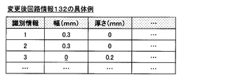
- FIG. 11 is a diagram showing a specific example of the changed circuit information 132.
- FIG. 12 is a diagram showing a specific example of the circuit information 131.
- FIG. 13 is a diagram showing details of the electromagnetic field analysis process according to the first embodiment.
- FIG. 14 is a diagram showing details of the electromagnetic field analysis process in the first embodiment.
- FIG. 15 is a diagram showing details of the electromagnetic field analysis process in the first embodiment.
- FIG. 16 is a diagram showing details of the electromagnetic field analysis process according to the first embodiment.
- FIG. 1 is a diagram showing a configuration of an information processing system 10.
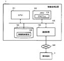
- the information processing system 10 shown in FIG. 1 has an information processing device 1 and an operation terminal 2.
- the operation terminal 2 is a terminal that can access the information processing device 1 via the network NW, and may be, for example, a PC (Personal Computer) or the like in which the developer inputs necessary information.
- a PC Personal Computer
- the information processing device 1 is, for example, one or more physical machines. Specifically, the information processing apparatus 1 performs electromagnetic field analysis on the wiring (for example, a line, a surface pattern, etc.) included in the electronic circuit board to be analyzed.
- the wiring for example, a line, a surface pattern, etc.
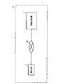
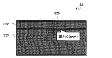
- FIG. 2 and 3 are diagrams illustrating a specific example of the electronic circuit board to be analyzed.
- FIG. 2 is a vertical cross-sectional view of the electronic circuit board S1
- FIG. 3 is a vertical cross-sectional view of the electronic circuit board S2.
- the electronic circuit board S1 and the electronic circuit board S2 are collectively referred to as the electronic circuit board S.
- the line S11 is arranged on the surface of the dielectric S12.
- the line S21 is arranged at a position sandwiched between the dielectric S22 and the dielectric S23 from above and below.
- the size of the width of the line S11 shown in FIG. 2 (the size of the line S11 in FIG. 2 in the left-right direction) and the size of the thickness of the line S11 (the size of the line S11 in FIG. 2 in the vertical direction).
- the minimum length scale for the geometric structure of the electronic circuit board S1 is the large width or thickness of the line S11. Determined by the track.
- the size of the width of the line S21 shown in FIG. 3 (the size of the line S21 in FIG. 3 in the left-right direction) and the size of the thickness of the line S21 (the size of the line S21 in FIG. 3 in the vertical direction).
- the minimum length scale for the geometric structure of the electronic circuit board S2 is the size of the width or thickness of the line S21. Determined by the track.
- the minimum in -plane length scale of the electronic circuit board S is on the order of 100 (mm) to 10 -1 ( mm), whereas the minimum in the plane of the electronic circuit board S is the minimum.
- the minimum length scale in the wiring shape in each direction may differ greatly, as in the case where the length scale of is on the order of about 10-2 (mm). Therefore, when the circuit included in the electronic circuit board S is discretized (mesh division), the minimum discretization step width of the space may become extremely small depending on the width and thickness of the line. In this case, the discretization step width of time may be reduced due to the necessity of satisfying the CFL condition, and the amount of calculation required for performing the electromagnetic field analysis may be increased.
- the information processing apparatus 1 in the present embodiment refers to, for example, circuit information about the circuit included in the electronic circuit board S (hereinafter, also referred to as first circuit information), and the width of the line included in the circuit information. Identify the size and thickness of the. Then, the information processing apparatus 1 changes one of the specified width size and the thickness size to zero based on the ratio of the specified width size and the thickness size (hereinafter, changed circuit information). Second circuit information) is generated. After that, the information processing apparatus 1 executes the electromagnetic field analysis based on the generated second circuit information.
- the characteristics of the circuit included in the electronic circuit board S are determined by, for example, the size of the width and thickness of the line, the size of the thickness of the layers constituting the electronic circuit board S, and the characteristic impedance based on the relative permittivity. Will be done. Therefore, for example, when the size of the thickness of the line and the size of the width of the line are significantly different, it can be determined that the smaller size of the thickness and width of the line has a small effect on the characteristic impedance.
- the size of the line thickness is sufficiently smaller than the size of the line width, even if the size of the line thickness is changed to a smaller size, after the discretization has been performed. It can be judged that the influence on the characteristics of the circuit is small.
- the size of the width of the line is sufficiently smaller than the size of the thickness of the line, even if the size of the width of the line is changed to a smaller size, the circuit after the discretization is performed. It can be judged that the influence on the characteristics of is small.
- the information processing apparatus 1 in the present embodiment replaces the line with a two-dimensional PEC (Perfect Electrical Controller). After changing the size of the thickness to zero, the circuit included in the electronic circuit board S is dissociated. Further, in the information processing apparatus 1 in the present embodiment, when the size of the width of the line is sufficiently smaller than the size of the thickness of the line, the size of the width of the line is increased by replacing the line with a two-dimensional PEC. Is changed to zero, and then the circuit included in the electronic circuit board S is discretized.
- PEC Perfect Electrical Controller
- the information processing apparatus 1 in the present embodiment can prevent the minimum length scale for the electronic circuit board S from being determined by the smaller size of the width and the thickness of the wiring. become. Therefore, the information processing apparatus 1 can prevent the minimum discretization step width of the space from becoming extremely small when the circuit included in the electronic circuit board S is discretized.
- the information processing apparatus 1 can prevent the discretized step width of the time determined by the CFL condition from becoming smaller by increasing the minimum discretized step width of the space.
- the information processing apparatus 1 can suppress the problem size when performing electromagnetic field analysis, and can suppress an increase in the amount of calculation required for electromagnetic field analysis.
- FIG. 4 is a diagram showing a hardware configuration of the information processing device 1.
- the information processing device 1 has a CPU 101 which is a processor, a memory 102, a communication device 103, and a storage medium 104.
- the parts are connected to each other via the bus 105.
- the storage medium 104 has, for example, a program storage area (not shown) for storing a program 110 for performing a process of performing an electromagnetic field analysis on a circuit included in the electronic circuit board S (hereinafter, also referred to as an electromagnetic field analysis process). Further, the storage medium 104 has, for example, an information storage area 130 for storing information used when performing electromagnetic field analysis processing.
- the storage medium 104 may be, for example, an HDD (Hard Disk Drive) or an SSD (Solid State Drive).
- the CPU 101 executes the program 110 loaded from the storage medium 104 into the memory 102 to perform electromagnetic field analysis processing.
- the communication device 103 communicates with the operation terminal 2 via, for example, the network NW.
- FIG. 5 is a block diagram of the function of the information processing apparatus 1.
- the information processing apparatus for example, hardware such as a CPU 101 and a memory 102 and a program 110 organically cooperate with each other to form an information receiving unit 111, an information management unit 112, and information.
- Various functions including the generation unit 113 and the analysis execution unit 114 are realized.
- the information processing apparatus 1 stores, for example, the circuit information 131 and the changed circuit information 132 in the information storage area 130, as shown in FIG.
- the information receiving unit 111 receives, for example, the circuit information 131 transmitted by the developer via the operation terminal 2. Then, the information management unit 112 stores, for example, the circuit information 131 received by the information receiving unit 111 in the information storage area 130.
- the information generation unit 113 refers to, for example, the circuit information 131 stored in the information storage area 130, and specifies the size of the width and the size of the thickness of the line included in the electronic circuit board S. Then, the information generation unit 113 is the circuit information 131 in which one of the specified width size and the thickness size is changed to zero based on the ratio of the specified width size and the thickness size. Generate circuit information 132. Then, the information management unit 112 stores, for example, the changed circuit information 132 generated by the information generation unit 113 in the information storage area 130.
- the analysis execution unit 114 refers to, for example, the changed circuit information 132 stored in the information storage area 130, and performs electromagnetic field analysis included in the electronic circuit board to be analyzed.
- FIG. 6 is a flowchart showing an outline of the electromagnetic field analysis process according to the first embodiment.
- the information processing apparatus 1 waits until the analysis timing is reached (NO in S101).
- the analysis timing may be, for example, the timing at which the developer inputs information to the effect that the electromagnetic field analysis is started via the operation terminal 2.
- the information processing apparatus 1 specifies the size of the width and the size of the thickness of the line included in the circuit information 131 (S102).
- the information processing apparatus 1 sets one of the width size or the thickness size specified in the processing of S102 to zero based on the ratio of the width size and the thickness size specified in the processing of S102.
- the changed circuit information 132 after the change is generated (S103).
- the information processing apparatus 1 executes the electromagnetic field analysis based on the changed circuit information 132 generated in the process of S103 (S104).
- the information processing apparatus 1 in the present embodiment can prevent the minimum length scale for the electronic circuit board S from being determined by the smaller size of the width and the thickness of the wiring. become. Therefore, the information processing apparatus 1 can prevent the minimum discretization step width of the space from becoming extremely small when the circuit included in the electronic circuit board S is discretized.
- the information processing apparatus 1 can prevent the discretized step width of the time determined by the CFL condition from becoming smaller by increasing the minimum discretized step width of the space.
- the information processing apparatus 1 can suppress the problem size when performing electromagnetic field analysis, and can suppress an increase in the amount of calculation required for electromagnetic field analysis.
- FIGS. 10 to 16 are diagrams showing details of the electromagnetic field analysis process in the first embodiment.
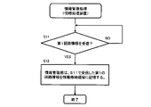
- FIG. 7 is a flowchart illustrating the information management process.
- the information receiving unit 111 of the information processing apparatus 1 waits until the circuit information 131 is received (NO in S11). Specifically, the information receiving unit 111 waits until, for example, the circuit information 131 input by the developer via the operation terminal 2 is received.
- the information management unit 112 of the information processing apparatus 1 stores the circuit information 131 received in the process of S11 in the information storage area 130 (S12).
- FIG. 10 is a diagram showing a specific example of the circuit information 131.
- the circuit information 131 shown in FIG. 10 includes, for example, "identification information” for identifying each line including the electronic circuit board S, "width” in which the width of each line is set, and the thickness of each line. It has a “thickness” in which the size of is set as an item.
- the information on the first line in the circuit information 131 shown in FIG. 10 will be described as being information corresponding to the line S11 arranged on the electronic circuit board S1 described with reference to FIG. Further, the information on the second line in the circuit information 131 shown in FIG. 10 will be described as being information corresponding to the line S21 arranged on the electronic circuit board S2 described with reference to FIG. That is, hereinafter, it is assumed that the width and thickness of the line S11 described with reference to FIG. 2 are "0.3 (mm)” and “0.035 (mm)”. Further, it is assumed that the width and thickness of the line S21 described with reference to FIG. 3 are "0.3 (mm)” and "0.018 (mm)”.
- the circuit information 131 is, for example, a surface arranged on the electronic circuit board S. It may include information about the pattern (width and thickness of the surface pattern, etc.).
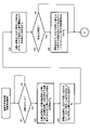
- the information generation unit 113 of the information processing apparatus 1 waits until the analysis timing is reached (NO in S21).
- the analysis timing may be, for example, the timing at which the developer inputs information to the effect that the electromagnetic field analysis is started via the operation terminal 2.
- the information generation unit 113 specifies a combination of the width and thickness of the line containing the information in the circuit information 131 stored in the information storage area 130. (S22).
- the circuit information 131 shown in FIG. 10 includes, for example, information about a line whose "identification information” is “1" (information on the first line) and a line whose "identification information” is “2". (Information on the second line) and information about. Therefore, the information generation unit 113 is, for example, "0.3 (mm)" and "0" which are the information set in the "width” and the “thickness” of the information in which "1" is set in the "identification information”. Specify the combination of ".035 (mm)”.
- the information generation unit 113 has, for example, "0.3 (mm)" and "0.” Which are information set in “width” and “thickness” of information in which "2" is set in “identification information”. 018 (mm) ”combination is specified.
- the information generation unit 113 also specifies the combination of the width size and the thickness size of the surface pattern. May be good.
- the information processing apparatus 1 may also perform the processing for the surface pattern in the processing after S23.
- the information generation unit 113 divides, for example, the size of the width specified in the process of S22 by the size of the thickness specified in the process of S22 for each combination specified in the process of S22 (S23).
- the information generation unit 113 specifies, for example, a combination whose value calculated in the process of S23 is equal to or greater than the threshold value among the combinations specified in the process of S22 (S24).
- the information generation unit 113 is among the information included in the circuit information 131 stored in the information storage area 130.
- the changed circuit information 132 is generated by setting the size of the thickness of the line corresponding to the combination specified in the process of S24 to zero (S26).
- the information generation unit 113 does not perform the process of S26.
- FIG. 11 is a diagram showing a specific example of the changed circuit information 132.
- the changed circuit information 132 shown in FIG. 11 is information generated by changing the circuit information 131 shown in FIG.
- the non-thick line S14 is arranged on the electronic circuit board S1 instead of the thick line S11. Is shown. Further, as for the information in the second line in the changed circuit information 132 shown in FIG. 11, as shown in FIG. 13, the non-thick line S25 is arranged on the electronic circuit board S2 instead of the thick line S21. Is shown.
- the information generation unit 113 specifies, for example, a combination specified in the process of S22 in which the reciprocal of the value calculated in the process of S23 is equal to or greater than the threshold value (S31).
- the information generation unit 113 contains information contained in the circuit information 131 stored in the information storage area 130.
- the changed circuit information 132 is generated by setting the size of the width of the line corresponding to the combination specified in the process of S31 to zero (S33).
- the information generation unit 113 does not perform the processing in S33.
- FIG. 14 is a diagram showing a specific example of the changed circuit information 132.
- the changed circuit information 132 shown in FIG. 14 is information generated by changing the circuit information 131 shown in FIG.
- the information generation unit 113 sets the size of the width of the line corresponding to the information whose "identification information” is "3" to zero. decide.
- the information generation unit 113 sets the “thickness” of the information (information in the third line) in which the “identification information” is “3” to “0 (). mm) ”.
- the analysis execution unit 114 of the information processing apparatus 1 refers to the changed circuit information 132 stored in the information storage area 130, and discretizes each line containing the information in the changed circuit information 132. (S34).
- the analysis execution unit 114 refers to the changed circuit information 132 stored in the information storage area 130, and for example, zero of the width and thickness of the line included in the electronic circuit board S is zero.
- the unset size is determined as the minimum discretized step size in space.
- the analysis execution unit 114 performs mesh division for the three-dimensional space including the electronic circuit board S so that the minimum discretized step width of the determined space becomes the mesh width, for example.
- the analysis execution unit 114 performs an electromagnetic field analysis for each line that has been discretized by the processing of S34 (S35).
- the analysis execution unit 114 calculates the discrete step size of time from the minimum discrete step size of the space determined in the process of S34. More specifically, the analysis execution unit 114 sets the discretization step width of time to be smaller than the time constant calculated by dividing the minimum discretization step width of space by the speed of light according to the CFL condition. The discretized step size is calculated. Then, the analysis execution unit 114 performs electromagnetic field analysis on the electronic circuit board S by using the discretized step size of the calculated time.
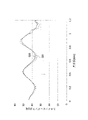
- FIGS. 15 and 16 are diagrams showing the effect of changing the thickness of the line included in the electronic circuit board S.
- FIG. 15 is a diagram showing the effect of changing the line S11 included in the electronic circuit board S1 described with reference to the line S14
- FIG. 16 is a diagram showing the influence of changing the line S11 to the line S14
- FIG. 16 is a diagram showing the effect of changing the line S11 included in the electronic circuit board S2 described with reference to FIG. It is a figure which shows the influence by changing S21 to the line S25.
- the horizontal axis and the vertical axis in FIGS. 15 and 16 indicate the frequency and the input impedance, respectively.
- the vertical size (layer thickness) of the dielectric S12 in FIG. 2 is “0.166 (mm)”
- the vertical size of the dielectric S22 in FIG. 3 is “0.216 (”. mm) ”
- it is assumed that the vertical size of the dielectric S23 in FIG. 3 is“ 0.784 (mm) ”.
- the input impedance when the line S11 is used (that is, the input impedance in the state of FIG. 2) and the input impedance when the line S14 is used (that is, in the state of FIG. 12). It shows that the difference from the input impedance) is about 2 ( ⁇ ) at the maximum.
- the input impedance when the line S21 is used (that is, the input impedance in the state of FIG. 3) and the input impedance when the line S25 is used (that is, the input impedance in the state of FIG. 13) are shown.
- the examples shown in FIGS. 15 and 16 show that the outlines of the graphs match in a broad sense. Further, in the examples shown in FIGS. 15 and 16, the difference in input impedance in each graph is about 2 to 3 ( ⁇ ), which is sufficient for the average value of input impedance (about 45 ( ⁇ )) in each graph. It shows that it is small. Therefore, it can be determined that the examples shown in FIGS. 15 and 16 show that the influence on the characteristic impedance is small even when the thickness of the line arranged on the electronic circuit board S is changed to zero.
- the information processing apparatus 1 in the present embodiment refers to the circuit information 131 about the circuit included in the electronic circuit board (not shown) to be analyzed, and the width of the wiring in which the information is included in the circuit information 131. Specify the size and thickness. Then, the information processing apparatus 1 generates the changed circuit information 132 in which one of the specified width size and the thickness size is changed to zero based on the ratio of the specified width size and the thickness size. do. After that, the information processing apparatus 1 executes the electromagnetic field analysis based on the generated second circuit information.
- the characteristics of the circuit included in the electronic circuit board S are determined by, for example, the size of the width and thickness of the line, the size of the thickness of the layers constituting the electronic circuit board S, and the characteristic impedance based on the relative permittivity. Will be done. Therefore, for example, when the size of the thickness of the line and the size of the width of the line are significantly different, it can be determined that the smaller size of the thickness and width of the line has a small effect on the characteristic impedance.
- the size of the line thickness is sufficiently smaller than the size of the line width, even if the size of the line thickness is changed to a smaller size, after the discretization has been performed. It can be judged that the influence on the characteristics of the circuit is small.
- the size of the width of the line is sufficiently smaller than the size of the thickness of the line, even if the size of the width of the line is changed to a smaller size, the circuit after the discretization is performed. It can be judged that the influence on the characteristics of is small.
- the information processing apparatus 1 in the present embodiment replaces the line with a two-dimensional PEC to increase the thickness of the line. After changing the value to zero, the circuit included in the electronic circuit board S is discretized. Further, in the information processing apparatus 1 in the present embodiment, when the size of the width of the line is sufficiently smaller than the size of the thickness of the line, the size of the width of the line is increased by replacing the line with a two-dimensional PEC. Is changed to zero, and then the circuit included in the electronic circuit board S is discretized.
- the information processing apparatus 1 in the present embodiment can prevent the minimum length scale for the electronic circuit board S from being determined by the smaller size of the width and the thickness of the wiring. become. Therefore, the information processing apparatus 1 can prevent the minimum discretization step width of the space from becoming extremely small when the circuit included in the electronic circuit board S is discretized.
- the total number of grids can be suppressed, and the minimum discretization step width of the space can be increased.
- mesh division is performed to make the grid spacing uneven, the spacing between adjacent grids cannot be changed significantly, but even in this case, the total number of grids can be suppressed, and the space is minimized. It is possible to increase the discretization step size.
- the information processing apparatus 1 can prevent the discretized step width of the time determined by the CFL condition from becoming smaller by increasing the minimum discretized step width of the space.
- the information processing apparatus 1 can suppress the problem size when performing electromagnetic field analysis, and can suppress an increase in the amount of calculation required for electromagnetic field analysis.
- the information processing apparatus 1 in the present embodiment uses, for example, the current distribution of the circuit specified in the electromagnetic field analysis in the present embodiment as a feature amount, so that the training data used for generating the above machine learning model can be generated. It may be one that performs generation.
- Information processing device 2 Operation terminal 10: Information processing system NW: Network
Landscapes
- Engineering & Computer Science (AREA)
- Computer Hardware Design (AREA)
- Physics & Mathematics (AREA)
- Theoretical Computer Science (AREA)
- General Engineering & Computer Science (AREA)
- General Physics & Mathematics (AREA)
- Evolutionary Computation (AREA)
- Geometry (AREA)
- Microelectronics & Electronic Packaging (AREA)
- Software Systems (AREA)
- Medical Informatics (AREA)
- Computer Vision & Pattern Recognition (AREA)
- Artificial Intelligence (AREA)
- Design And Manufacture Of Integrated Circuits (AREA)
Priority Applications (4)
| Application Number | Priority Date | Filing Date | Title |
|---|---|---|---|
| JP2022553323A JP7364969B2 (ja) | 2020-09-30 | 2020-09-30 | 電磁場解析プログラム、電磁場解析装置及び電磁場解析方法 |
| EP20956257.8A EP4224357A4 (en) | 2020-09-30 | 2020-09-30 | ELECTROMAGNETIC FIELD ANALYSIS PROGRAM, ELECTROMAGNETIC FIELD ANALYSIS DEVICE, AND ELECTROMAGNETIC FIELD ANALYSIS METHOD |
| PCT/JP2020/037206 WO2022070329A1 (ja) | 2020-09-30 | 2020-09-30 | 電磁場解析プログラム、電磁場解析装置及び電磁場解析方法 |
| US18/176,875 US20230204650A1 (en) | 2020-09-30 | 2023-03-01 | Storage medium, electromagnetic field analysis device, and electromagnetic field analysis method |
Applications Claiming Priority (1)
| Application Number | Priority Date | Filing Date | Title |
|---|---|---|---|
| PCT/JP2020/037206 WO2022070329A1 (ja) | 2020-09-30 | 2020-09-30 | 電磁場解析プログラム、電磁場解析装置及び電磁場解析方法 |
Related Child Applications (1)
| Application Number | Title | Priority Date | Filing Date |
|---|---|---|---|
| US18/176,875 Continuation US20230204650A1 (en) | 2020-09-30 | 2023-03-01 | Storage medium, electromagnetic field analysis device, and electromagnetic field analysis method |
Publications (1)
| Publication Number | Publication Date |
|---|---|
| WO2022070329A1 true WO2022070329A1 (ja) | 2022-04-07 |
Family
ID=80949959
Family Applications (1)
| Application Number | Title | Priority Date | Filing Date |
|---|---|---|---|
| PCT/JP2020/037206 Ceased WO2022070329A1 (ja) | 2020-09-30 | 2020-09-30 | 電磁場解析プログラム、電磁場解析装置及び電磁場解析方法 |
Country Status (4)
| Country | Link |
|---|---|
| US (1) | US20230204650A1 (https=) |
| EP (1) | EP4224357A4 (https=) |
| JP (1) | JP7364969B2 (https=) |
| WO (1) | WO2022070329A1 (https=) |
Citations (4)
| Publication number | Priority date | Publication date | Assignee | Title |
|---|---|---|---|---|
| JP2003076741A (ja) * | 2001-06-20 | 2003-03-14 | Nec Corp | プリント回路基板設計支援装置、方法およびプログラム |
| JP2005107870A (ja) * | 2003-09-30 | 2005-04-21 | Fujitsu Ltd | 解析モデル作成装置 |
| JP2006040308A (ja) | 2001-06-20 | 2006-02-09 | Nec Corp | プリント回路基板設計支援装置、方法およびプログラム |
| JP2006053908A (ja) | 2004-07-15 | 2006-02-23 | Fujitsu Ltd | シミュレーション手法 |
Family Cites Families (2)
| Publication number | Priority date | Publication date | Assignee | Title |
|---|---|---|---|---|
| US7093206B2 (en) * | 2003-10-21 | 2006-08-15 | International Business Machines Corp. | Computer aided design method and apparatus for modeling and analyzing on-chip interconnect structures |
| JP2013171361A (ja) * | 2012-02-20 | 2013-09-02 | Elpida Memory Inc | 電気特性評価解析システム、等価回路モデル抽出方法、並びに、それらのプログラム及び記録媒体 |
-
2020
- 2020-09-30 EP EP20956257.8A patent/EP4224357A4/en active Pending
- 2020-09-30 JP JP2022553323A patent/JP7364969B2/ja active Active
- 2020-09-30 WO PCT/JP2020/037206 patent/WO2022070329A1/ja not_active Ceased
-
2023
- 2023-03-01 US US18/176,875 patent/US20230204650A1/en active Pending
Patent Citations (4)
| Publication number | Priority date | Publication date | Assignee | Title |
|---|---|---|---|---|
| JP2003076741A (ja) * | 2001-06-20 | 2003-03-14 | Nec Corp | プリント回路基板設計支援装置、方法およびプログラム |
| JP2006040308A (ja) | 2001-06-20 | 2006-02-09 | Nec Corp | プリント回路基板設計支援装置、方法およびプログラム |
| JP2005107870A (ja) * | 2003-09-30 | 2005-04-21 | Fujitsu Ltd | 解析モデル作成装置 |
| JP2006053908A (ja) | 2004-07-15 | 2006-02-23 | Fujitsu Ltd | シミュレーション手法 |
Also Published As
| Publication number | Publication date |
|---|---|
| EP4224357A1 (en) | 2023-08-09 |
| US20230204650A1 (en) | 2023-06-29 |
| JP7364969B2 (ja) | 2023-10-19 |
| JPWO2022070329A1 (https=) | 2022-04-07 |
| EP4224357A4 (en) | 2023-11-15 |
Similar Documents
| Publication | Publication Date | Title |
|---|---|---|
| JP5320101B2 (ja) | プリント基板の設計方法及びプリント基板の設計支援装置 | |
| TWI384379B (zh) | 用於評估在實體系統中所產生之波傳播的電腦實施方法和裝置及電腦可讀儲存媒體 | |
| US8601428B2 (en) | System and method for use case-based thermal analysis of heuristically determined component combinations and layouts in a portable computing device | |
| US9129075B2 (en) | Mesh generation system | |
| JPWO2020095362A1 (ja) | 設計支援装置、設計支援方法および機械学習装置 | |
| US9715571B1 (en) | Systems and methods for simulations of reliability in printed circuit boards | |
| JP5359226B2 (ja) | 物理的システムで生ずる波動伝播を評価する方法及び装置 | |
| CN114491983A (zh) | 电磁干扰屏蔽罩缝隙设计方法、装置、设备及存储介质 | |
| US10140399B2 (en) | Corner database generator | |
| US20160117199A1 (en) | Computing system with thermal mechanism and method of operation thereof | |
| de Carvalho et al. | Similarity‐based clustering for patterns of extreme values | |
| US10089151B2 (en) | Apparatus, method, and program medium for parallel-processing parameter determination | |
| US20100014569A1 (en) | Identifying An Optimized Test Bit Pattern For Analyzing Electrical Communications Channel Topologies | |
| JP7364969B2 (ja) | 電磁場解析プログラム、電磁場解析装置及び電磁場解析方法 | |
| US20250225290A1 (en) | Method, apparatus, device and storage medium for evaluating power supply design | |
| WO2023103678A1 (zh) | 时钟信号电路设计方法、装置、存储介质及电子设备 | |
| WO2013114911A1 (ja) | リスク評価システム、リスク評価方法、及びプログラム | |
| KR20210087594A (ko) | 고전압 정션 블록의 emi 차폐 성능 시뮬레이션 장치 및 방법 | |
| US10929177B2 (en) | Managing resources for multiple trial distributed processing tasks | |
| US20230205975A1 (en) | Storage medium, equivalent circuit analysis apparatus, and equivalent circuit analysis method | |
| JP2015090628A (ja) | 機器配置自動算出装置 | |
| US20250193198A1 (en) | Resource access security | |
| JP6421447B2 (ja) | 解析装置、解析プログラム、および解析方法 | |
| JP2025087438A (ja) | Emc対策システム及びemc対策方法 | |
| CN121658227A (zh) | 一种容量规划方法、装置、设备和存储介质 |
Legal Events
| Date | Code | Title | Description |
|---|---|---|---|
| 121 | Ep: the epo has been informed by wipo that ep was designated in this application |
Ref document number: 20956257 Country of ref document: EP Kind code of ref document: A1 |
|
| ENP | Entry into the national phase |
Ref document number: 2022553323 Country of ref document: JP Kind code of ref document: A |
|
| NENP | Non-entry into the national phase |
Ref country code: DE |
|
| ENP | Entry into the national phase |
Ref document number: 2020956257 Country of ref document: EP Effective date: 20230502 |