WO2022049752A1 - ヘテロ接合バイポーラトランジスタおよびその製造方法 - Google Patents
ヘテロ接合バイポーラトランジスタおよびその製造方法 Download PDFInfo
- Publication number
- WO2022049752A1 WO2022049752A1 PCT/JP2020/033722 JP2020033722W WO2022049752A1 WO 2022049752 A1 WO2022049752 A1 WO 2022049752A1 JP 2020033722 W JP2020033722 W JP 2020033722W WO 2022049752 A1 WO2022049752 A1 WO 2022049752A1
- Authority
- WO
- WIPO (PCT)
- Prior art keywords
- layer
- collector
- electrode
- base
- emitter
- Prior art date
- Legal status (The legal status is an assumption and is not a legal conclusion. Google has not performed a legal analysis and makes no representation as to the accuracy of the status listed.)
- Ceased
Links
Images





Classifications
-
- H—ELECTRICITY
- H10—SEMICONDUCTOR DEVICES; ELECTRIC SOLID-STATE DEVICES NOT OTHERWISE PROVIDED FOR
- H10D—INORGANIC ELECTRIC SEMICONDUCTOR DEVICES
- H10D10/00—Bipolar junction transistors [BJT]
- H10D10/80—Heterojunction BJTs
- H10D10/821—Vertical heterojunction BJTs
-
- H—ELECTRICITY
- H10—SEMICONDUCTOR DEVICES; ELECTRIC SOLID-STATE DEVICES NOT OTHERWISE PROVIDED FOR
- H10D—INORGANIC ELECTRIC SEMICONDUCTOR DEVICES
- H10D64/00—Electrodes of devices having potential barriers
- H10D64/20—Electrodes characterised by their shapes, relative sizes or dispositions
- H10D64/27—Electrodes not carrying the current to be rectified, amplified, oscillated or switched, e.g. gates
- H10D64/281—Base electrodes for bipolar transistors
-
- H—ELECTRICITY
- H10—SEMICONDUCTOR DEVICES; ELECTRIC SOLID-STATE DEVICES NOT OTHERWISE PROVIDED FOR
- H10D—INORGANIC ELECTRIC SEMICONDUCTOR DEVICES
- H10D10/00—Bipolar junction transistors [BJT]
- H10D10/01—Manufacture or treatment
- H10D10/021—Manufacture or treatment of heterojunction BJTs [HBT]
-
- H—ELECTRICITY
- H10—SEMICONDUCTOR DEVICES; ELECTRIC SOLID-STATE DEVICES NOT OTHERWISE PROVIDED FOR
- H10D—INORGANIC ELECTRIC SEMICONDUCTOR DEVICES
- H10D10/00—Bipolar junction transistors [BJT]
- H10D10/80—Heterojunction BJTs
-
- H—ELECTRICITY
- H10—SEMICONDUCTOR DEVICES; ELECTRIC SOLID-STATE DEVICES NOT OTHERWISE PROVIDED FOR
- H10D—INORGANIC ELECTRIC SEMICONDUCTOR DEVICES
- H10D62/00—Semiconductor bodies, or regions thereof, of devices having potential barriers
- H10D62/10—Shapes, relative sizes or dispositions of the regions of the semiconductor bodies; Shapes of the semiconductor bodies
- H10D62/13—Semiconductor regions connected to electrodes carrying current to be rectified, amplified or switched, e.g. source or drain regions
- H10D62/137—Collector regions of BJTs
-
- H—ELECTRICITY
- H10—SEMICONDUCTOR DEVICES; ELECTRIC SOLID-STATE DEVICES NOT OTHERWISE PROVIDED FOR
- H10D—INORGANIC ELECTRIC SEMICONDUCTOR DEVICES
- H10D62/00—Semiconductor bodies, or regions thereof, of devices having potential barriers
- H10D62/10—Shapes, relative sizes or dispositions of the regions of the semiconductor bodies; Shapes of the semiconductor bodies
- H10D62/17—Semiconductor regions connected to electrodes not carrying current to be rectified, amplified or switched, e.g. channel regions
- H10D62/177—Base regions of bipolar transistors, e.g. BJTs or IGBTs
-
- H—ELECTRICITY
- H10—SEMICONDUCTOR DEVICES; ELECTRIC SOLID-STATE DEVICES NOT OTHERWISE PROVIDED FOR
- H10D—INORGANIC ELECTRIC SEMICONDUCTOR DEVICES
- H10D62/00—Semiconductor bodies, or regions thereof, of devices having potential barriers
- H10D62/80—Semiconductor bodies, or regions thereof, of devices having potential barriers characterised by the materials
- H10D62/82—Heterojunctions
- H10D62/824—Heterojunctions comprising only Group III-V materials heterojunctions, e.g. GaN/AlGaN heterojunctions
-
- H—ELECTRICITY
- H10—SEMICONDUCTOR DEVICES; ELECTRIC SOLID-STATE DEVICES NOT OTHERWISE PROVIDED FOR
- H10D—INORGANIC ELECTRIC SEMICONDUCTOR DEVICES
- H10D64/00—Electrodes of devices having potential barriers
- H10D64/20—Electrodes characterised by their shapes, relative sizes or dispositions
- H10D64/23—Electrodes carrying the current to be rectified, amplified, oscillated or switched, e.g. sources, drains, anodes or cathodes
- H10D64/231—Emitter or collector electrodes for bipolar transistors
Definitions
- the present invention relates to a heterojunction bipolar transistor and a method for manufacturing the same.
- Indium phosphide (InP) -based heterojunction bipolar transistor (HBT) is a transistor with excellent high speed that is suitable for integrated circuits for optical / wireless communication.
- InP-based HBT it is important to reduce the intrinsic capacitance and the parasitic capacitance by miniaturizing the element while maintaining the operating current amount, and to shorten the charge / discharge time.
- the junction temperature of the element increases due to miniaturization. Since the junction temperature is a factor that has a great influence not only on direct electrical characteristics such as electron speed and current gain but also on long-term reliability, heat dissipation measures are indispensable for increasing the speed of HBT.
- Non-Patent Document 1 discloses an HBT as shown in FIG. This HBT includes a metal layer 302 formed on the heat radiating substrate 301, a sub-collector layer 303, a collector layer 304, a base layer 305, an emitter layer 306, and an emitter cap layer 307 formed on the metal layer 302. .
- An emitter electrode 308 is formed on the emitter cap layer 307, and a base electrode 309 is formed on the base layer 305 around the emitter layer 306. Further, the metal layer 302 functions as a collector electrode.
- a part of the base electrode 309 forms a so-called base pad structure formed in a wider area in order to connect to the upper layer wiring (not shown). is doing.
- the heat generated inside the HBT is generally dissipated from the collector layer 304 toward the heat dissipation substrate 301 by heat conduction in the solid.
- the layer (metal layer 302) on the side of the heat dissipation substrate 301 with respect to the sub-collector layer 303 is more heat than the compound semiconductor constituting the emitter layer 306, the base layer 305, the collector layer 304, and the sub-collector layer 303. Since it is made of a material having high conductivity, the heat dissipation of the HBT can be improved.
- Non-Patent Document 1 it is difficult to accurately reduce the collector parasitic capacitance generated between the base electrode 309 of the base pad structure and the metal layer 302 serving as the collector electrode, which limits the speedup. A new issue arises. The details will be described below.
- the first is to reduce the area of the base pad structure, and the second is to remove the semiconductor layer (base layer, collector layer, sub-collector layer) existing between the base electrode and the collector electrode of the base pad structure. It is to be.
- the contact position accuracy between the upper layer wiring and the base pad electrode and the dimensional variation of the contact hole are used.
- an area of about 1 ⁇ m 2 is typically required. Therefore, significantly reducing the base pad structure by the first method may cause other problems such as poor connection and short circuit between terminals.
- the material of the base layer, the collector layer, and the sub-collector layer is used.
- a method of removing by wet etching using a chemical solution corresponding to the above is adopted.
- the etching amount per hour is greatly affected by the etching conditions such as the temperature and concentration of the chemical solution, the area and density of the surface to be etched, and the crystal orientation. Therefore, for example, in a region where the transistor density is different in the wafer surface, the amount of side etching of the semiconductor layer directly under the base pad structure varies, and as a result, the parasitic collector capacity of the transistor may vary in the wafer surface.
- the parasitic collector capacity cannot be significantly reduced.
- the base pad electrode end bends toward the substrate due to the weight of the base pad electrode and the stress at the time of formation, and in the worst case, the base pad electrode and the collector electrode are bent. There is a concern that the contact will cause an electrical short circuit between the base electrode and the collector electrode.
- the base pad structure itself acts as a shield, and it is difficult to observe the side etching amount of the semiconductor layer directly underneath without destruction with an electron microscope or the like, so it is also difficult to optimize the wet etching time.
- the present invention has been made to solve the above problems, and an object thereof is to enable the parasitic collector capacity in the base pad structure to be reduced without sacrificing high speed.
- the heterojunction bipolar transistor according to the present invention is a compound having a collector electrode formed on a substrate in an area smaller than the substrate in plan view and a compound formed on the collector electrode in an area smaller than the collector electrode in plan view.
- An emitter layer made of a compound semiconductor formed in an area smaller than the base layer visually, an emitter cap layer made of a compound semiconductor formed on the emitter layer, and an emitter electrode formed on the emitter cap layer.
- an emitter cap forming layer, an emitter forming layer, a base forming layer, a collector forming layer, and a sub-collector made of a compound semiconductor are placed on a growth substrate made of a compound semiconductor, respectively.
- a sub-collector layer, a collector layer, a base layer, an emitter layer having an area smaller than the base layer in a plan view, and an emitter cap layer are formed on the metal layer.
- the base pad electrode extends outside the base layer in a plan view to form the base pad electrode, and the extending portion of the base pad electrode is supported by the support portion.
- Parasitic collector capacity can be reduced without sacrificing high speed.
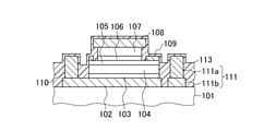
- FIG. 1 is a cross-sectional view showing the configuration of a heterojunction bipolar transistor according to an embodiment of the present invention.
- FIG. 2A is a cross-sectional view showing a state of an element in an intermediate process for explaining a method for manufacturing a heterojunction bipolar transistor according to an embodiment of the present invention.
- FIG. 2B is a cross-sectional view showing a state of an element in an intermediate process for explaining a method for manufacturing a heterojunction bipolar transistor according to an embodiment of the present invention.
- FIG. 2C is a cross-sectional view showing a state of an element in an intermediate process for explaining a method for manufacturing a heterojunction bipolar transistor according to an embodiment of the present invention.
- FIG. 2A is a cross-sectional view showing a state of an element in an intermediate process for explaining a method for manufacturing a heterojunction bipolar transistor according to an embodiment of the present invention.
- FIG. 2B is a cross-sectional view showing a state of an element in an intermediate process for
- FIG. 2D is a cross-sectional view showing a state of an element in an intermediate process for explaining a method for manufacturing a heterojunction bipolar transistor according to an embodiment of the present invention.
- FIG. 2E is a cross-sectional view showing a state of an element in an intermediate process for explaining a method for manufacturing a heterojunction bipolar transistor according to an embodiment of the present invention.
- FIG. 2F is a cross-sectional view showing a state of an element in an intermediate process for explaining a method for manufacturing a heterojunction bipolar transistor according to an embodiment of the present invention.
- FIG. 2G is a cross-sectional view showing a state of an element in an intermediate process for explaining a method for manufacturing a heterojunction bipolar transistor according to an embodiment of the present invention.
- FIG. 2H is a cross-sectional view showing a state of an element in an intermediate process for explaining a method for manufacturing a heterojunction bipolar transistor according to an embodiment of the present invention.
- FIG. 2I is a cross-sectional view showing a state of an element in an intermediate process for explaining a method for manufacturing a heterojunction bipolar transistor according to an embodiment of the present invention.
- FIG. 3 is a cross-sectional view showing the configuration of a conventional heterojunction bipolar transistor.
- This heterojunction bipolar transistor first includes a collector electrode 102 formed on a substrate 101 in an area smaller than that of the substrate 101 in a plan view.
- the substrate 101 is made of a material used as a heat dissipation substrate in this kind of technical field.
- the collector electrode 102 is formed in contact with the substrate 101.
- the substrate 101 is preferably made of a material having a thermal conductivity higher than that of InP and having an insulating property equivalent to that of InP in order to facilitate electrical separation between elements.
- the substrate 101 can be composed of, for example, Si, AlN, GaN, SiC, diamond, or a laminated structure in which these materials are combined.
- the collector electrode 102 is made of, for example, a metal designated as Au / Ti or Au / Mo from the side of the substrate 101.
- this HBT is formed on the collector electrode 102 in an area smaller than that of the collector electrode 102 in plan view, and is formed on the sub-collector layer 103 made of the compound semiconductor and the compound semiconductor formed on the sub-collector layer 103. It includes a collector layer 104 made of a collector layer 104 and a base layer 105 made of a compound semiconductor formed on the collector layer 104. In this example, the sub-collector layer 103 is formed in contact with the collector electrode 102.
- the sub-collector layer 103, the collector layer 104, and the base layer 105 are formed in the same area in a plan view, and these form the first mesa.
- the first mesa is, for example, a columnar shape having a rectangular shape in a plan view.
- the sub-collector layer 103 is composed of, for example, n + -InGaAs in which Si is heavily doped to form an n-type.
- the collector layer 104 is composed of, for example, n-InGaAs in which Si is doped at a low concentration to form an n-type.
- the base layer 105 is composed of, for example, p + -GaAsSb in which C is heavily doped to form a p-type.
- this HBT is composed of an emitter layer 106 made of a compound semiconductor formed on a base layer 105 in an area smaller than that of the base layer 105 in a plan view, and a compound semiconductor formed on the emitter layer 106. It is provided with an emitter cap layer 107.
- the emitter layer 106 and the emitter cap layer 107 are formed in the same area in a plan view, and these form a second mesa.
- the second mesa is, for example, a columnar shape having a rectangular shape in a plan view.
- the second mesa is arranged inside the first mesa in a plan view.
- the emitter layer 106 is composed of n-InP which is doped with Si at a low concentration to form an n-type.
- the emitter cap layer 107 is composed of n + -InGaAs, which is formed into an n-type by doping with a high concentration of Si.
- this HBT includes an emitter electrode 108 formed on the emitter cap layer 107 and a base electrode 109 formed on the base layer 105 around the emitter layer 106.
- the emitter electrode 108 can be made of a metal such as Mo / W.
- the base electrode 109 can be made of a metal such as Au / Ti.
- this HBT includes a support portion 111, a collector post electrode 110, and a base pad electrode 112.
- the collector post electrode 110 is formed on the collector electrode 102 around the sub collector layer 103.
- the base pad electrode 112 is electrically connected to the base electrode 109 and is formed so as to extend outward from the base layer 105 (first mesa) in a plan view.
- the second mesa is arranged on the first mesa with the side of the support portion 111 as a wider area.
- the base electrode 109 also has a wider area on the side of the support portion 111.
- the base pad electrode 112 is connected to the base electrode 109 in this wider area.
- the support portion 111 is formed on the substrate 101 around the collector electrode 102, separated from the collector electrode 102. Further, the support portion 111 supports the extending portion of the base pad electrode 112 on the collector electrode 102. In other words, the base pad electrode 112 is erected between the support portion 111 and the base electrode 109 formed on the side of the support portion 111.
- the support portion 111 is formed in a columnar shape, for example.
- the support portion 111 is composed of a first support portion 111a and a second support portion 111b.
- the first support portion 111a is formed on the second support portion 111b.
- the support portion 111 (first support portion 111a) is formed higher than the base electrode 109 with respect to the surface of the substrate 101.
- the second support portion 111b can be made of the same material as the collector electrode 102.
- the first support portion 111a can be made of the same material as the collector post electrode 110.
- the first support portion 111a can be formed at the same time.
- this HBT includes a protective layer 113 formed by covering an element portion including a collector electrode 102, a sub-collector layer 103, a collector layer 104, a base layer 105, an emitter layer 106, and an emitter cap layer 107.
- the protective layer 113 is made of, for example, a resin such as benzocyclobutene (BCB).
- the base pad electrode 112 is formed on the protective layer 113 around the element portion.
- the upper portions of the emitter electrode 108 and the base electrode 109 are exposed from the protective layer 113.
- the upper portion of the collector post electrode 110 is exposed from the protective layer 113.
- the upper portion of the support portion 111 (first support portion 111a) is exposed from the protective layer 113.
- the base pad electrode 112 is in contact with and supported on the upper portion of the exposed support portion 111.
- the relative permittivity is directly below the base pad electrode 112 extending outside the base layer 105 (first mesa) in a plan view in a region other than the base electrode 109. There is no high semiconductor layer.
- the protective layer 113 having a relative permittivity lower than that of the semiconductor layer is formed in this region. As a result, the parasitic collector capacity generated in the base pad electrode 112 can be accurately reduced.
- connection portion between the base electrode 109 and the base pad electrode 112
- the parasitic collector capacity generated in the region of this connection portion can be minimized.
- the support portion 111 is composed of the first support portion 111a and the second support portion 111b.
- the second support portion 111b can be formed, for example, in the same process as the collector electrode 102.
- the collector post electrode 110 can be formed in the first support portion 111a in the same process.
- the HBT according to the embodiment can be manufactured by adding a minimum number of steps to the conventional manufacturing process of the HBT on the heat dissipation substrate. Further, the height of the collector post electrode 110 and the height of the base pad electrode 112 with respect to the surface of the substrate 101 can be made equal to each other.
- an interlayer insulating film is formed, and the interlayer insulating film on the collector post electrode 110 and the base pad electrode 112 is removed. , Form wiring metal.
- the interlayer insulating film on the collector post electrode 110 and the base pad electrode 112 can be removed under the same conditions. , The number of processes can be reduced.
- the support portion 111 from metal, the heat generated by the element is dissipated to the substrate 101 via the base electrode 109, the base pad electrode 112, and the support portion 111. Is newly formed, and it is possible to further improve the heat dissipation of the element formed on the substrate 101.
- the parasitic collector capacity in the base pad structure can be reduced without sacrificing high speed (high frequency characteristics). Further, according to the embodiment, the base pad structure can be formed uniformly in the wafer surface.
- an emitter cap forming layer 131, an emitter forming layer 132, a base forming layer 133, and a collector forming layer 134, respectively, made of a compound semiconductor are placed on a growth substrate 151 made of a compound semiconductor (made of InP).
- the sub-collector cambium 135 are formed by crystal growth in this order (first step).
- Sub-collector cambium 135 is sequentially epitaxially grown on the growth substrate 151.
- the above-mentioned epitaxial growth of each layer can be performed by the organometallic vapor phase deposition method or the molecular beam epitaxy method. Since each of the above-mentioned layers can be epitaxially grown on the growth substrate 151 made of InP in a lattice-matched state, good crystallinity with few dislocations and defects can be obtained.
- a metal layer 136 made of metal is formed on the sub-collector forming layer 135 (second step).
- the metal layer 136 can be formed by depositing these metals as a composite structure of Ti / Au or Mo / Au from the side in contact with the sub-collector forming layer 135 by using a vacuum vapor deposition method or a sputtering method.
- Ti or Mo good adhesion between the sub-collector cambium 135 made of InGaAs and the metal layer 136 can be obtained.
- the HBT element forming layer does not peel off from the substrate 101 due to heat or mechanical stress generated in the HBT element forming step described later.
- the material of the metal layer 136 can be made of a material that can be bonded at a temperature equal to or lower than the maximum allowable temperature of HBT, which will be described later.
- the substrate 101 is bonded onto the metal layer 136 (third step).
- the metal layer 136 and the introduced metal layer can be formed on the side of the substrate 101, and the metal layers can be bonded (bonded) to each other.
- the bonding (bonding) method known techniques such as a surface activation bonding method and an atomic diffusion bonding method can be used.
- the removal of the growth substrate 151 can be carried out by using known mechanical polishing or wet etching using a hydrochloric acid-based chemical solution.
- the growth substrate 151 is removed (fourth step) to expose the surface of the emitter cap forming layer 131 as shown in FIG. 2D.
- the sub-collector forming layer 135, the collector forming layer 134, the base forming layer 133, the emitter forming layer 132, and the emitter cap forming layer 131 are formed on the substrate 101 via the metal layer 136.
- a sub-collector layer 103, a collector layer 104, a base layer 105, an emitter layer 106, an emitter cap layer 107, an emitter electrode 108, and a base electrode 109 are formed on the metal layer 136. (Fifth step).
- a resist pattern having an opening at a location to be the emitter electrode 108 is formed on the emitter cap forming layer 131 by patterning by photolithography. Then, the emitter electrode material is deposited by the vacuum vapor deposition method. After that, by lifting off the resist pattern, the emitter electrode 108 can be formed on the emitter cap forming layer 131.
- the emitter layer 106 is formed by patterning the emitter forming layer 132 and the emitter cap forming layer 131.
- the emitter layer 106 and the emitter cap layer 107 are formed in the same area in a plan view to form a second mesa.
- the emitter cap layer 107 and the emitter layer 106 can be formed by etching the emitter cap forming layer 131 and the emitter forming layer 132 with a citric acid-based etchant and a hydrochloric acid-based etchant, respectively, using the emitter electrode 108 as a mask.
- the citric acid-based etchant hardly etches the emitter cambium 132 made of InP.
- the hydrochloric acid-based etchant hardly etches the emitter cap layer 107 made of InGaAs and the base forming layer 133 made of GaAsSb. Therefore, by using the above etchant, the emitter cap layer 107 and the emitter layer 106 can be formed individually.
- the base electrode 109 is formed on the base forming layer 133 (base layer 105) around the emitter layer 106.
- the base electrode 109 can be formed by the same manufacturing method (lift-off method) as the emitter electrode 108.
- One of the base electrodes 109 formed on both sides of the emitter layer 106 is formed slightly wider than the other to serve as a connection portion of the base pad electrode 112. This is to provide a margin of alignment accuracy when forming the base pad electrode 112, which will be described later.
- the parasitic collector capacity increases as the area of the region for this connection increases, it is desirable to narrow the area of the above-mentioned region as long as it can be connected to the base pad electrode 112 with good yield in terms of high frequency characteristics.
- the sub-collector layer 103, the collector layer 104, and the base layer 105 are formed by patterning the sub-collector forming layer 135, the collector forming layer 134, and the base forming layer 133.
- the base layer 105 is formed so that the emitter layer 106 and the emitter cap layer 107 have an area smaller than that of the base layer 105 in a plan view.
- the sub-collector layer 103, the collector layer 104, and the base layer 105 are formed in the same area in a plan view to be used as the first mesa.
- the base layer 105, the collector layer 104, and the sub-collector layer 103 use a resist mask patterned in the same manner as the emitter electrode 108, and the base forming layer 133, the collector forming layer 134, and the sub collector forming layer 135 are respectively citric acid-based etching. It can be formed by etching with a hydrochloric acid-based etchant or a citric acid-based etchant.
- the collector post electrode 110 and the collector post electrode 110 are placed on the metal layer 136 around the element portion including the sub-collector layer 103, the collector layer 104, the base layer 105, the emitter layer 106, and the emitter cap layer 107.
- the first support portion 111a is formed (sixth step).
- the collector post electrode 110 and the first support portion 111a can be formed by the lift-off method described above.
- the collector post electrode 110 and the first support portion 111a having an appropriate thickness (height), the connection with the upper layer wiring can be facilitated. It is desirable that the thickness is at least thicker than the total of the sub-collector layer 103, the collector layer 104, and the base layer 105.
- the first support portion 111a is formed to be equal to or higher than the base electrode 109.
- the metal layer 136 is separated into a region where the first support portion 111a is formed, a region of the element portion, and a region of the first support portion 111a, and as shown in FIG. 2G, the collector electrode 102 and the metal layer 136 are separated from each other.
- the second support portion 111b is formed (7th step).
- a second support portion 111b is formed on the substrate 101 around the collector electrode 102 so as to be separated from the collector electrode 102.
- the collector electrode 102 and the second support portion 111b can be formed by patterning the metal layer 136 by an etching process using a predetermined resist pattern as a mask.
- metals such as Ti and Mo can be etched by fluorine-based dry etching.
- Au can be etched by wet etching using an iodine-based chemical solution or ion milling using an Ar-based gas.
- the collector electrode 102 is arranged on the substrate 101 below the element portion.
- the second support portion 111b is arranged on the substrate 101 under the first support portion 111a.
- the support portion 111 is configured from the first support portion 111a and the second support portion 111b. Further, the support portion 111 is formed on the substrate 101 around the collector electrode 102 apart from the collector electrode 102.
- the protective layer 113 covering the element portion is formed (step 8).
- the protective layer 113 can be formed by spin-coating BCB to form a coating film and heat-treating the coating film at a high temperature to cure it.
- the viscosity of the BCB and the spin coat rotation speed are adjusted so that the design thickness of the protective layer 113 at this stage is thinner than the total thickness of the collector electrode 102, the sub-collector layer 103, the collector layer 104, and the base layer 105.
- a protective layer 113 having a design thickness is formed on the substrate 101 on which the element portion is not formed, while a region higher than the design thickness (specifically, the emitter electrode 108, the base electrode 109, and the support portion) is formed. 111, the protective layer 113 is formed on the collector post electrode 110 in a very thin state.
- the upper part of the base electrode 109, the upper part of the collector post electrode 110, and the upper part of the support portion 111 are exposed from the protective layer 113 (9th step). For example, by etching back the entire area (entire surface) of the protective layer 113, the upper portion of the base electrode 109, the upper portion of the collector post electrode 110, and the upper portion of the support portion 111 can be exposed from the protective layer 113.
- the protective layer 113 By forming the protective layer 113 to an appropriate thickness when forming the protective layer 113, only the upper portion of the base electrode 109, the upper portion of the collector post electrode 110, and the upper portion of the support portion 111 can be exposed.
- the base pad electrode 112 formed on the side of the support portion 111 and connected to the base electrode 109 exposed from the protective layer 113 and extending to the outside of the base layer 105 and above the support portion 111 in a plan view is provided.
- the heterojunction bipolar transistor described with reference to FIG. 1 is obtained.
- the base pad electrode 112 can be formed by the lift-off method described above.
- the base pad electrode is formed extending outside the base layer in a plan view, and the extending portion of the base pad electrode is supported by the support portion.
- the base pad electrode is installed between the base electrode and the base electrode, and the parasitic collector capacity in the base pad structure can be reduced without sacrificing high speed.
- the present invention is not limited to the embodiments described above, and many modifications and combinations can be carried out by a person having ordinary knowledge in the art within the technical idea of the present invention. That is clear.
- the npn-type InP / GaAsSb-based HBT on a heat-dissipating substrate which is promising for realizing an ultra-high-speed integrated circuit, has been described in detail, but the same effect is also effective for other HBTs.
Landscapes
- Bipolar Transistors (AREA)
Abstract
HBTは、基板(101)の上に、コレクタ電極(102)、サブコレクタ層(103)、コレクタ層(104)、ベース層(105)、エミッタ層(106)、エミッタキャップ層(107)、エミッタ電極(108)、ベース電極(109)を備え、ベースパッド電極(112)が、ベース電極(109)に電気的に接続し、平面視でベース層(105)より外側に延在して形成され、支持部(111)は、コレクタ電極(102)の上でベースパッド電極(112)の延在部を支持している。
Description
本発明は、ヘテロ接合バイポーラトランジスタおよびその製造方法に関する。
インジウムリン(InP)系ヘテロ接合バイポーラトランジスタ(HBT)は、光/無線通信用集積回路に適した、高速性に優れたトランジスタである。InP系HBTの更なる高速化を実現するためには、動作電流量を維持しつつ、素子微細化により真性容量および寄生容量を削減し、充放電時間を短縮することが重要となる。一方で、微細化により素子の熱抵抗が増大することから、素子の接合温度(素子内部の温度)は、微細化により増加する。接合温度は、電子速度や電流利得といった直接的な電気的特性だけでなく、長期信頼性に対しても大きな影響を与える要因となるため、HBT高速化において放熱対策は必須事項である。
HBTの放熱性の向上には、例えば非特許文献1に示されている技術がある。非特許文献1には、図3に示すようなHBTが開示されている。このHBTは、放熱基板301の上に形成された金属層302と、金属層302の上に形成されたサブコレクタ層303、コレクタ層304、ベース層305、エミッタ層306、エミッタキャップ層307を備える。エミッタキャップ層307の上には、エミッタ電極308が形成され、エミッタ層306の周囲のベース層305の上には、ベース電極309が形成されている。また、金属層302が、コレクタ電極として機能する。
上述した構成のHBTにおいて、非特許文献1の技術では、ベース電極309の一部が、図視していない上層配線と接続するために、より広い面積に形成された、いわゆるベースパッド構造を成している。
HBT内部で発生した熱は、一般的にコレクタ層304から放熱基板301の側に向かって固体中の熱伝導により放熱される。上記の構造によれば、サブコレクタ層303より放熱基板301の側の層(金属層302)は、エミッタ層306、ベース層305、コレクタ層304、サブコレクタ層303を構成する化合物半導体よりも熱伝導率が高い材料で構成されていることから、HBTの放熱性を向上させることができる。
しかしながら、非特許文献1の構造において、ベースパッド構造のベース電極309とコレクタ電極となる金属層302との間に生じるコレクタ寄生容量を精度良く削減することが困難なため、高速化に制約が生じるという新たな課題が生じる。以下にその詳細を説明する。
一般的に、ベースパッド構造の寄生容量を削減する方法は大きく2つ考えられる。第1に、ベースパッド構造の面積を縮小することであり、第2に、ベースパッド構造のベース電極とコレクタ電極との間に存在する半導体層(ベース層、コレクタ層、サブコレクタ層)を除去することである。
一般に、ベースパッド構造においては、エミッタ幅0.25μm級のヘテロ接合バイポーラトランジスタを製造する際に使用する露光技術を用いた場合、上層配線とベースパッド電極とのコンタクト位置精度やコンタクトホールの寸法ばらつきなどを考慮すると、典型的には1μm2程度の面積が必要とされる。このため、第1の方法により、ベースパッド構造を大幅に縮小することは、接続不良や端子間のショートといった別種の問題を引き起こす可能性がある。
ベースパッド構造と上部配線の接続工程のみ、解像度の高い露光技術を用いることで、原理的にはベースパッド構造の縮小化を図ることは可能である。しかしながら、この1工程のために高解像度の露光装置を導入することは、プロセスコストの増大を招く。このため、素子形成工程と同等の露光技術で、上層配線と歩留まりよく接続可能な面積を有するベースパッド構造が望ましいことは言うまでもない。
また、第2の方法として挙げたベースパッド構造直下の半導体層(ベース層、コレクタ層、サブコレクタ層)を除去するためには、典型的には、ベース層、コレクタ層、サブコレクタ層の材料に対応した薬液を用いたウェットエッチングにより除去する方法が採られる。しかしながら、ウェットエッチングは、薬液温度や濃度、被エッチング面の面積や密度、結晶方位などのエッチング条件によって、時間当たりのエッチング量が大きく影響を受ける。このため、例えば、ウェハ面内でトランジスタ密度が異なる領域では、ベースパッド構造直下の半導体層のサイドエッチング量にばらつきが生じ、結果としてウェハ面内においてトランジスタの寄生コレクタ容量ばらつきが生じる要因となりうる。
サイドエッチ量が不足すれば、有意に寄生コレクタ容量を削減することはできない。一方、ベースパッド電極直下の半導体層が過剰にサイドエッチされた場合、ベースパッド電極の自重や形成時の応力によりベースパッド電極端が基板側にたわみ、最悪の場合、ベースパッド電極とコレクタ電極が接触することで、ベース電極とコレクタ電極が電気的に短絡することが懸念される。
加えて、ベースパッド構造そのものが遮蔽物となり、直下の半導体層のサイドエッチング量を電子顕微鏡等により非破壊で観察することが困難なために、ウェットエッチング時間の最適化も困難である。
Y. Shiratori et al., "High-Speed InP/InGaAsSb DHBT on High-Thermal-Conductivity SiC Substrate", IEEE Electron Device Letters, vol. 39, no. 6, pp. 807-810, 2018.
以上に説明したように、放熱性を改善するために放熱基板上にInP系HBTを形成する場合において、ベースパッド構造直下の寄生コレクタ容量をウェハ面内で均一性良く削減することが難しく、高速化に制限が生じるという課題がある。
本発明は、以上のような問題点を解消するためになされたものであり、ベースパッド構造における寄生コレクタ容量が、高速性を犠牲にすることなく低減できるようにすることを目的とする。
本発明に係るヘテロ接合バイポーラトランジスタは、基板の上に、平面視で基板より小さい面積に形成されたコレクタ電極と、コレクタ電極の上に、平面視でコレクタ電極より小さい面積に形成された、化合物半導体からなるサブコレクタ層と、サブコレクタ層の上に形成された、化合物半導体からなるコレクタ層と、コレクタ層の上に形成された、化合物半導体からなるベース層と、ベース層の上に、平面視でベース層より小さい面積に形成された、化合物半導体からなるエミッタ層と、エミッタ層の上に形成された、化合物半導体からなるエミッタキャップ層と、エミッタキャップ層の上に形成されたエミッタ電極と、エミッタ層の周囲のベース層の上に形成されたベース電極と、サブコレクタ層の周囲のコレクタ電極の上に形成されたコレクタポスト電極と、ベース電極に接続し、平面視でベース層より外側に延在して形成されたベースパッド電極と、コレクタ電極から離間して、コレクタ電極の周囲の基板の上に形成され、コレクタ電極の上でベースパッド電極の延在部を支持する支持部とを備える。
また、本発明に係るヘテロ接合バイポーラトランジスタの製造方法は、化合物半導体からなる成長基板の上に、各々化合物半導体からなるエミッタキャップ形成層、エミッタ形成層、ベース形成層、コレクタ形成層、およびサブコレクタ形成層を、これらの順に結晶成長して形成する第1工程と、サブコレクタ形成層の上に金属からなる金属層を形成する第2工程と、金属層の上に、基板を貼り合わせる第3工程と、金属層の上に基板を貼り合わせた後で、成長基板を除去する第4工程と、基板の上に金属層を介して形成された、サブコレクタ形成層、コレクタ形成層、ベース形成層、エミッタ形成層、エミッタキャップ形成層をパターニングすることで、金属層の上に、サブコレクタ層、コレクタ層、ベース層、平面視でベース層より小さい面積のエミッタ層、エミッタキャップ層を形成し、エミッタキャップ層の上にエミッタ電極を形成し、エミッタ層の周囲のベース層の上にベース電極を形成する第5工程と、サブコレクタ層、コレクタ層、ベース層、エミッタ層、エミッタキャップ層を備える素子部の周囲の金属層の上に、コレクタポスト電極および第1支持部を形成する第6工程と、金属層を、第1支持部が形成されている領域と素子部の領域と、第1支持部の領域とに分離して、素子部の下の基板の上に配置されたコレクタ電極と、第1支持部の下の基板の上に配置された第2支持部とを形成し、第1支持部と第2支持部とから構成された支持部を、コレクタ電極から離間して、コレクタ電極の周囲の基板の上に形成する第7工程と、素子部を覆う保護層を形成する第8工程と、ベース電極の上部、コレクタポスト電極の上部、および支持部の上部を、保護層より露出させる第9工程と、支持部の側に形成され、保護層より露出したベース電極に接続し、平面視で、ベース層より外側で支持部の上にまで延在するベースパッド電極を、保護層の上に形成する第10工程とを備える。
以上説明したように、本発明によれば、平面視でベース層より外側に延在してベースパッド電極を形成し、ベースパッド電極の延在部を支持部で支持するので、ベースパッド構造における寄生コレクタ容量が、高速性を犠牲にすることなく低減できる。
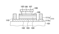
以下、本発明の実施の形態に係るヘテロ接合バイポーラトランジスタについて図1を参照して説明する。
このヘテロ接合バイポーラトランジスタ(HBT)は、まず、基板101の上に、平面視で基板101より小さい面積に形成されたコレクタ電極102を備える。基板101は、この種の技術分野で、放熱基板とされる材料から構成されている。この例では、基板101の上に接して、コレクタ電極102が形成されている。
基板101は、例えば、InPよりも熱伝導率が高く、かつ素子間の電気的分離を容易にするために、InPと同等の絶縁性を有している材料から構成することが望ましい。基板101は、例えば、Si、AlN、GaN、SiC、ダイヤモンド、あるいはこれらの材料を組み合わせた積層構造から構成することができる。また、コレクタ電極102は、例えば、基板101の側からAu/Tiあるいは、Au/Moとされた金属から構成されている。
また、このHBTは、コレクタ電極102の上に、平面視でコレクタ電極102より小さい面積に形成された、化合物半導体からなるサブコレクタ層103と、サブコレクタ層103の上に形成された、化合物半導体からなるコレクタ層104と、コレクタ層104の上に形成された、化合物半導体からなるベース層105とを備える。この例では、コレクタ電極102の上に接して、サブコレクタ層103が形成されている。
サブコレクタ層103,コレクタ層104,ベース層105は、平面視で同一の面積に形成されて、これらで、第1メサが構成されている。第1メサは、例えば、平面視矩形の柱状とされている。サブコレクタ層103は、例えば、Siが高濃度にドープされてn型とされたn+-InGaAsから構成されている。コレクタ層104は、例えば、Siが低濃度にドープされてn型とされたn-InGaAsから構成されている。ベース層105は、例えば、Cが高濃度にドープされてp型とされたp+-GaAsSbから構成されている。
また、このHBTは、ベース層105の上に、平面視でベース層105より小さい面積に形成された、化合物半導体からなるエミッタ層106と、エミッタ層106の上に形成された、化合物半導体からなるエミッタキャップ層107とを備える。エミッタ層106、エミッタキャップ層107は、平面視で同一の面積に形成されて、これらで、第2メサが構成されている。第2メサは、例えば、平面視矩形の柱状とされている。第2メサは、平面視で、第1メサの内側に配置されている。
例えば、エミッタ層106は、Siが低濃度にドープされてn型とされたn-InPから構成されている。また、エミッタキャップ層107は、Siが高濃度にドープされてn型とされたn+-InGaAsから構成されている。
また、このHBTは、エミッタキャップ層107の上に形成されたエミッタ電極108と、エミッタ層106の周囲のベース層105の上に形成されたベース電極109とを備える。エミッタ電極108は、Mo/Wなどの金属から構成することができる。ベース電極109は、Au/Tiなどの金属から構成することができる。
上述した構成に加え、このHBTは、支持部111、コレクタポスト電極110、ベースパッド電極112を備える。
コレクタポスト電極110は、サブコレクタ層103の周囲のコレクタ電極102の上に形成されている。ベースパッド電極112は、ベース電極109に電気的に接続し、平面視でベース層105(第1メサ)より外側に延在して形成されている。この例では、第1メサの上で、支持部111の側をより広い面積として、第2メサが配置されている。また、ベース電極109も、支持部111の側をより広い面積とされている。このより広い面積とされている領域のベース電極109に、ベースパッド電極112が接続している。
支持部111は、コレクタ電極102から離間して、コレクタ電極102の周囲の基板101の上に形成されている。また、支持部111は、コレクタ電極102の上でベースパッド電極112の延在部を支持している。言い換えると、ベースパッド電極112は、支持部111と、支持部111の側に形成されたベース電極109との間に架設されている。支持部111は、例えば、柱状に形成されている。
なお、この例において、支持部111は、第1支持部111aと第2支持部111bとから構成されている。第1支持部111aは、第2支持部111bの上に形成されている。また、支持部111(第1支持部111a)は、基板101の表面を基準として、ベース電極109より高く形成されている。例えば、第2支持部111bは、コレクタ電極102と同じ材料から構成することができる。例えば、コレクタ電極102を形成するときに、同時に、第2支持部111bを形成することができる。また、第1支持部111aは、コレクタポスト電極110と同じ材料から構成することができる。例えば、コレクタポスト電極110を形成するときに、同時に、第1支持部111aを形成することができる。
また、このHBTは、コレクタ電極102、サブコレクタ層103、コレクタ層104、ベース層105、エミッタ層106、およびエミッタキャップ層107を備える素子部を覆って形成された保護層113を備える。保護層113は、例えば、ベンゾシクロブテン(BCB)などの樹脂から構成されている。ここで、ベースパッド電極112は、素子部の周囲の保護層113の上に形成されている。なお、エミッタ電極108、ベース電極109の上部は、保護層113より露出している。また、コレクタポスト電極110の上部は、保護層113より露出している。また、支持部111(第1支持部111a)の上部は、保護層113より露出している。この露出している支持部111の上部に、ベースパッド電極112が接触して支持されている。
実施の形態によれば、原理的に、ベース電極109以外の領域の、平面視でベース層105(第1メサ)より外側に延在しているベースパッド電極112の直下には、比誘電率が高い半導体層は存在しない。実施の形態では、この領域に、比誘電率が半導体層より低い保護層113が形成されている。この結果、ベースパッド電極112で生じる寄生コレクタ容量を、精度よく削減することができる。
また、ベース電極109とベースパッド電極112との接続部の幅を狭くすることで、この接続部の領域で生じる寄生コレクタ容量も最小限にすることができる。この構成では、この接続部直下のベース層105、コレクタ層104、サブコレクタ層103に、アンダーカット構造を適用する必要はないため、寄生コレクタ容量のばらつきを最小限に抑えることもできる。
ここで、実施の形態では、支持部111を、第1支持部111aと第2支持部111bとから構成している。第2支持部111bは、例えば、コレクタ電極102と同一工程で形成可能である。また、第1支持部111aは、コレクタポスト電極110を、同一工程で形成可能である。このように、実施の形態によれば、従来の放熱基板上のHBTの製造工程に対して、最小限度の工程を追加するだけで、実施の形態に係るHBTが製造できる。また、基板101の表面を基準とした、コレクタポスト電極110の高さと、ベースパッド電極112の高さとを、同等にすることが可能である。
これにより上層配線と、ベースパッド電極112との接続工程も容易になる。例えば、上層配線を形成する際には、図1を用いて説明した素子の構造を形成し後に、層間絶縁膜を形成し、コレクタポスト電極110およびベースパッド電極112上の層間絶縁膜を除去し、配線金属を形成する。この際、コレクタポスト電極110およびベースパッド電極112の、基板101からの高さがほぼ同等であれば、同一条件でコレクタポスト電極110およびベースパッド電極112上の層間絶縁膜を除去することができ、工程数を削減できる。
また、副次的にではあるが、支持部111を金属から構成することで、素子で発生した熱を、ベース電極109,ベースパッド電極112、および支持部111を介して基板101に放熱するパスが新たに形成され、基板101上に形成された素子の放熱性を、更に向上させることが可能である。
以上示したように、実施の形態によれば、ベースパッド構造における寄生コレクタ容量が、高速性(高周波特性)を犠牲にすることなく低減できるようになる。また、実施の形態によれば、ウェハ面内で均一性良くベースパッド構造を形成できる。
次に、本発明の実施の形態に係るヘテロ接合バイポーラトランジスタの製造方法について、図2A~図2Iを参照して説明する。
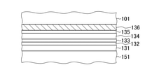
まず、図2Aに示すように、化合物半導体(InPからなる)からなる成長基板151の上に、各々化合物半導体からなるエミッタキャップ形成層131、エミッタ形成層132、ベース形成層133、コレクタ形成層134、およびサブコレクタ形成層135を、これらの順に結晶成長して形成する(第1工程)。
例えば、n+-InGaAsからなるエミッタキャップ形成層131、n-InPからなるエミッタ形成層132、p+-GaAsSbからなるベース形成層133、n-InGaAsからなるコレクタ形成層134、n+-InGaAsからなるサブコレクタ形成層135を、成長基板151の上に、順次にエピタキシャル成長する。例えば、有機金属気相堆積法や分子線エピタキシー法により、上述した各層のエピタキシャル成長ができる。上述した各層は、InPからなる成長基板151の上に格子整合した状態でエピタキシャル成長できるため、転位や欠陥の少ない良好な結晶性を得ることができる。
次に、図2Bに示すように、サブコレクタ形成層135の上に金属からなる金属層136を形成する(第2工程)。例えば、サブコレクタ形成層135に接する側からTi/Auあるいは、Mo/Auの複合構造として、真空蒸着法やスパッタ法を用いてこれら金属を堆積することで、金属層136が形成できる。TiやMoを用いることで、InGaAsからなるサブコレクタ形成層135と金属層136との良好な密着性が得られる。これにより、後述するHBTの素子形成工程において発生する熱や機械的応力によりHBT素子形成層が、基板101から剥離することがない。また、Auは、ヤング率が低く酸化しないため、後述する基板101と容易に接合させることができる。金属層136の材料は、後記する、基板101の貼り合わせが、HBTの最大許容温度以下で接合可能な材料から構成することができる。
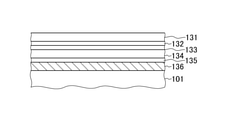
次に、図2Cに示すように、金属層136の上に、基板101を貼り合わせる(第3工程)。この貼り合わせにおいては、金属層136と導入の金属層を、基板101の側に形成しておき、金属層同士で張り合わせ(接合)を実施することができる。この貼り合わせ(接合)の方法としては、例えば、表面活性化接合法や原子拡散接合法などの、公知の技術を用いることができる。何れの接合技術においても、InP系HBTの最大プロセス温度(400℃)以下の接合温度で、接合を実施することが可能である。成長基板151の除去は、公知の機械研磨や塩酸系の薬液を用いたウェットエッチングを用いて実施することができる。
以上のように、金属層136に基板101を貼り合わせた後で、成長基板151を除去し(第4工程)、図2Dに示すように、エミッタキャップ形成層131の表面を露出させる。この結果、基板101の上に、金属層136を介して、サブコレクタ形成層135、コレクタ形成層134、ベース形成層133、エミッタ形成層132、エミッタキャップ形成層131が形成された状態となる。
次に、図2Eに示すように、金属層136の上に、サブコレクタ層103、コレクタ層104、ベース層105、エミッタ層106、エミッタキャップ層107、エミッタ電極108、およびベース電極109を形成する(第5工程)。
例えば、エミッタキャップ形成層131の上に、フォトリソグラフィによるパターニングで、エミッタ電極108とする箇所に開口を備えるレジストパターンを形成する。次いで、真空蒸着法により、エミッタ電極材料を堆積する。この後、レジストパターンをリフトオフすることにより、エミッタキャップ形成層131の上にエミッタ電極108が形成できる。
次いで、エミッタ形成層132、エミッタキャップ形成層131をパターニングすることで、エミッタ層106を形成する。エミッタ層106、エミッタキャップ層107は、平面視で同一の面積に形成して第2メサとする。
また、エミッタキャップ層107およびエミッタ層106は、エミッタ電極108をマスクとして、エミッタキャップ形成層131およびエミッタ形成層132を、それぞれクエン酸系エッチャント、塩酸系エッチャントを用いてエッチングすることで形成できる。クエン酸系エッチャントは、InPからなるエミッタ形成層132を殆どエッチングしない。また、塩酸系エッチャントはInGaAsからなるエミッタキャップ層107およびGaAsSbからなるベース形成層133を殆どエッチングしない。従って、上記エッチャントを用いることで、エミッタキャップ層107とエミッタ層106とを個別に形成することができる。
次に、エミッタ層106の周囲のベース形成層133(ベース層105)の上にベース電極109を形成する。ベース電極109は、エミッタ電極108と同様の製造方法(リフトオフ法)により形成することができる。なお、エミッタ層106の両脇に形成されたベース電極109の一方は、他方より少し幅広く形成し、ベースパッド電極112の接続部とする。これは、後述する、ベースパッド電極112を形成する際の位置合わせ精度のマージンをもたせるためである。ただし、この接続のための領域の面積が広がると寄生コレクタ容量が増大するため、ベースパッド電極112と歩留まりよく接続できる限りにおいて、上述した領域の面積を狭くすることが高周波特性上望ましい。
次いで、サブコレクタ形成層135、コレクタ形成層134、ベース形成層133をパターニングすることで、サブコレクタ層103、コレクタ層104、ベース層105を形成する。エミッタ層106、エミッタキャップ層107が、平面視でベース層105より小さい面積となるように、ベース層105を形成する。サブコレクタ層103,コレクタ層104,ベース層105は、平面視で同一の面積に形成して第1メサとする。
ベース層105、コレクタ層104、サブコレクタ層103は、エミッタ電極108と同様にパターニングしたレジストマスクを用いて、ベース形成層133、コレクタ形成層134、サブコレクタ形成層135をそれぞれクエン酸系エッチャント、塩酸系エッチャント、クエン酸系エッチャントを用いてエッチングすることで、形成できる。
次に、図2Fに示すように、サブコレクタ層103、コレクタ層104、ベース層105、エミッタ層106、エミッタキャップ層107を備える素子部の周囲の金属層136の上に、コレクタポスト電極110および第1支持部111aを形成する(第6工程)。例えば、前述したリフトオフ法により、コレクタポスト電極110および第1支持部111aが形成できる。適切な厚さ(高さ)のコレクタポスト電極110および第1支持部111aを形成することで、上層配線との接続を容易にすることができる。厚さとしては、少なくとも、サブコレクタ層103、コレクタ層104、およびベース層105の合計より厚くすることが望ましい。基板101の表面を基準として、第1支持部111aをベース電極109と同等かベース電極109より高く形成する。
次に、金属層136を、第1支持部111aが形成されている領域と素子部の領域と、第1支持部111aの領域とに分離して、図2Gに示すように、コレクタ電極102と第2支持部111bとを形成する(第7工程)。コレクタ電極102から離間して、コレクタ電極102の周囲の基板101の上に第2支持部111bを形成する。所定のレジストパターンをマスクとしたエッチング処理により、金属層136をパターニングすることで、コレクタ電極102および第2支持部111bが形成できる。例えば、TiやMoなどの金属は、フッ素系のドライエッチングによりエッチング処理ができる。また、Auは、ヨウ素系の薬液を用いたウェットエッチングあるいはAr系のガスを用いたイオンミリングによりエッチング処理ができる。
コレクタ電極102は、素子部の下の基板101の上に配置される。第2支持部111bは、第1支持部111aの下の基板101の上に配置される。第1支持部111aと第2支持部111bとから、支持部111が構成された状態となる。また、コレクタ電極102から離間して、コレクタ電極102の周囲の基板101の上に支持部111が形成せれた状態となる。
次に、図2Hに示すように、素子部を覆う保護層113を形成する(第8工程)。例えば、BCBをスピンコートして塗布膜を形成し、この塗布膜を高温で加熱処理して硬化することで、保護層113が形成できる。この段階における保護層113の設計厚さが、コレクタ電極102、サブコレクタ層103、コレクタ層104,ベース層105の合計厚さより薄くなるように、BCBの粘性やスピンコート回転数を調整する。これにより、素子部が形成されていない基板101の上には、設計厚の保護層113が形成され、一方で、設計厚より高い領域(具体的にはエミッタ電極108、ベース電極109、支持部111、コレクタポスト電極110上は、保護層113が非常に薄い状態に形成される。
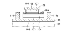
次に、図2Iに示すように、ベース電極109の上部、コレクタポスト電極110の上部、および支持部111の上部を、保護層113より露出させる(第9工程)。例えば、保護層113の全域(全面)をエッチバックすることで、ベース電極109の上部、コレクタポスト電極110の上部、および支持部111の上部を、保護層113より露出させることができる。保護層113の形成時に、適切な厚さに保護層113を形成することで、ベース電極109の上部、コレクタポスト電極110の上部、および支持部111の上部のみを露出させることができる。
次に、支持部111の側に形成され、保護層113より露出したベース電極109に接続し、平面視で、ベース層105より外側で支持部111の上にまで延在するベースパッド電極112を、保護層113の上に形成する(第10工程)。この結果、図1を用いて説明したヘテロ接合バイポーラトランジスタが得られる。例えば、前述したリフトオフ法により、ベースパッド電極112が形成できる。
以上に説明したように、本発明によれば、平面視でベース層より外側に延在してベースパッド電極を形成し、ベースパッド電極の延在部を支持部で支持するので、支持部とベース電極との間にベースパッド電極が架設されるものとなり、ベースパッド構造における寄生コレクタ容量が、高速性を犠牲にすることなく低減できるようになる。
なお、本発明は以上に説明した実施の形態に限定されるものではなく、本発明の技術的思想内で、当分野において通常の知識を有する者により、多くの変形および組み合わせが実施可能であることは明白である。例えば、上述では、超高速集積回路を実現する上で有望な放熱基板上のnpn型InP/GaAsSb系HBTについて詳細に述べたが、同様な効果は、他のHBTに対しても有効である。
101…基板、102…コレクタ電極、103…サブコレクタ層、104…コレクタ層、105…ベース層、106…エミッタ層、107…エミッタキャップ層、108…エミッタ電極、109…ベース電極、110…コレクタポスト電極、111…支持部、111a…第1支持部、111b…第2支持部、112…ベースパッド電極、113…保護層。
Claims (5)
- 基板の上に、平面視で前記基板より小さい面積に形成されたコレクタ電極と、
前記コレクタ電極の上に、平面視で前記コレクタ電極より小さい面積に形成された、化合物半導体からなるサブコレクタ層と、
前記サブコレクタ層の上に形成された、化合物半導体からなるコレクタ層と、
前記コレクタ層の上に形成された、化合物半導体からなるベース層と、
前記ベース層の上に、平面視で前記ベース層より小さい面積に形成された、化合物半導体からなるエミッタ層と、
前記エミッタ層の上に形成された、化合物半導体からなるエミッタキャップ層と、
前記エミッタキャップ層の上に形成されたエミッタ電極と、
前記エミッタ層の周囲の前記ベース層の上に形成されたベース電極と、
前記サブコレクタ層の周囲の前記コレクタ電極の上に形成されたコレクタポスト電極と、
前記ベース電極に接続し、平面視で前記ベース層より外側に延在して形成されたベースパッド電極と、
前記コレクタ電極から離間して、前記コレクタ電極の周囲の前記基板の上に形成され、前記コレクタ電極の上で前記ベースパッド電極の延在部を支持する支持部と
を備えるヘテロ接合バイポーラトランジスタ。 - 請求項1記載のヘテロ接合バイポーラトランジスタにおいて、
前記コレクタ電極、前記サブコレクタ層、前記コレクタ層、前記ベース層、前記エミッタ層、および前記エミッタキャップ層を備える素子部を覆って形成された保護層を備え、
前記ベースパッド電極は、前記素子部の周囲の前記保護層の上に形成されている
ことを特徴とするヘテロ接合バイポーラトランジスタ。 - 請求項1または2記載のヘテロ接合バイポーラトランジスタにおいて、
前記支持部は、前記基板の表面を基準として、前記ベース電極と同等か前記ベース電極より高く形成されていることを特徴とするヘテロ接合バイポーラトランジスタ。 - 化合物半導体からなる成長基板の上に、各々化合物半導体からなるエミッタキャップ形成層、エミッタ形成層、ベース形成層、コレクタ形成層、およびサブコレクタ形成層を、これらの順に結晶成長して形成する第1工程と、
前記サブコレクタ形成層の上に金属からなる金属層を形成する第2工程と、
前記金属層の上に、基板を貼り合わせる第3工程と、
前記金属層の上に基板を張り合わせた後で、前記成長基板を除去する第4工程と、
前記基板の上に前記金属層を介して形成された、前記サブコレクタ形成層、前記コレクタ形成層、前記ベース形成層、前記エミッタ形成層、前記エミッタキャップ形成層をパターニングすることで、前記金属層の上に、サブコレクタ層、コレクタ層、ベース層、平面視で前記ベース層より小さい面積のエミッタ層、エミッタキャップ層を形成し、前記エミッタキャップ層の上にエミッタ電極を形成し、前記エミッタ層の周囲の前記ベース層の上にベース電極を形成する第5工程と、
前記サブコレクタ層、前記コレクタ層、前記ベース層、前記エミッタ層、前記エミッタキャップ層を備える素子部の周囲の前記金属層の上に、コレクタポスト電極および第1支持部を形成する第6工程と、
前記金属層を、前記第1支持部が形成されている領域と前記素子部の領域と、前記第1支持部の領域とに分離して、前記素子部の下の前記基板の上に配置されたコレクタ電極と、前記第1支持部の下の前記基板の上に配置された第2支持部とを形成し、前記第1支持部と前記第2支持部とから構成された支持部を、前記コレクタ電極から離間して、前記コレクタ電極の周囲の前記基板の上に形成する第7工程と、
前記素子部を覆う保護層を形成する第8工程と、
前記ベース電極の上部、前記コレクタポスト電極の上部、および前記支持部の上部を、前記保護層より露出させる第9工程と、
前記支持部の側に形成され、前記保護層より露出した前記ベース電極に接続し、平面視で、前記ベース層より外側で前記支持部の上にまで延在するベースパッド電極を、前記保護層の上に形成する第10工程と
を備えるヘテロ接合バイポーラトランジスタの製造方法。 - 請求項4記載のヘテロ接合バイポーラトランジスタの製造方法において、
前記第6工程は、前記基板の表面を基準として、前記第1支持部を前記ベース電極と同等か前記ベース電極より高く形成することを特徴とするヘテロ接合バイポーラトランジスタの製造方法。
Priority Applications (3)
| Application Number | Priority Date | Filing Date | Title |
|---|---|---|---|
| US18/041,255 US20230307518A1 (en) | 2020-09-07 | 2020-09-07 | Hetero-Junction Bipolar Transistor and Method of Manufacturing the Same |
| JP2022546841A JP7480854B2 (ja) | 2020-09-07 | 2020-09-07 | ヘテロ接合バイポーラトランジスタおよびその製造方法 |
| PCT/JP2020/033722 WO2022049752A1 (ja) | 2020-09-07 | 2020-09-07 | ヘテロ接合バイポーラトランジスタおよびその製造方法 |
Applications Claiming Priority (1)
| Application Number | Priority Date | Filing Date | Title |
|---|---|---|---|
| PCT/JP2020/033722 WO2022049752A1 (ja) | 2020-09-07 | 2020-09-07 | ヘテロ接合バイポーラトランジスタおよびその製造方法 |
Publications (1)
| Publication Number | Publication Date |
|---|---|
| WO2022049752A1 true WO2022049752A1 (ja) | 2022-03-10 |
Family
ID=80490778
Family Applications (1)
| Application Number | Title | Priority Date | Filing Date |
|---|---|---|---|
| PCT/JP2020/033722 Ceased WO2022049752A1 (ja) | 2020-09-07 | 2020-09-07 | ヘテロ接合バイポーラトランジスタおよびその製造方法 |
Country Status (3)
| Country | Link |
|---|---|
| US (1) | US20230307518A1 (ja) |
| JP (1) | JP7480854B2 (ja) |
| WO (1) | WO2022049752A1 (ja) |
Citations (4)
| Publication number | Priority date | Publication date | Assignee | Title |
|---|---|---|---|---|
| US20040090834A1 (en) * | 2002-11-12 | 2004-05-13 | Yang Kyoung Hoon | Based pad layout for reducing parasitic base-collector capacitance and method of fabricating HBT using the same |
| JP2006310517A (ja) * | 2005-04-28 | 2006-11-09 | Korea Advanced Inst Of Sci Technol | 半導体装置のベースパッドのレイアウト構造、及びそれを用いたヘテロ接合型バイポーラトランジスタの製造方法 |
| JP2019054120A (ja) * | 2017-09-15 | 2019-04-04 | 株式会社村田製作所 | バイポーラトランジスタ及び高周波パワーアンプモジュール |
| WO2019208295A1 (ja) * | 2018-04-24 | 2019-10-31 | 日本電信電話株式会社 | バイポーラトランジスタおよびその製造方法 |
Family Cites Families (1)
| Publication number | Priority date | Publication date | Assignee | Title |
|---|---|---|---|---|
| JP2004327717A (ja) * | 2003-04-24 | 2004-11-18 | Sony Corp | 半導体装置およびその製造方法 |
-
2020
- 2020-09-07 JP JP2022546841A patent/JP7480854B2/ja active Active
- 2020-09-07 WO PCT/JP2020/033722 patent/WO2022049752A1/ja not_active Ceased
- 2020-09-07 US US18/041,255 patent/US20230307518A1/en not_active Abandoned
Patent Citations (4)
| Publication number | Priority date | Publication date | Assignee | Title |
|---|---|---|---|---|
| US20040090834A1 (en) * | 2002-11-12 | 2004-05-13 | Yang Kyoung Hoon | Based pad layout for reducing parasitic base-collector capacitance and method of fabricating HBT using the same |
| JP2006310517A (ja) * | 2005-04-28 | 2006-11-09 | Korea Advanced Inst Of Sci Technol | 半導体装置のベースパッドのレイアウト構造、及びそれを用いたヘテロ接合型バイポーラトランジスタの製造方法 |
| JP2019054120A (ja) * | 2017-09-15 | 2019-04-04 | 株式会社村田製作所 | バイポーラトランジスタ及び高周波パワーアンプモジュール |
| WO2019208295A1 (ja) * | 2018-04-24 | 2019-10-31 | 日本電信電話株式会社 | バイポーラトランジスタおよびその製造方法 |
Also Published As
| Publication number | Publication date |
|---|---|
| US20230307518A1 (en) | 2023-09-28 |
| JP7480854B2 (ja) | 2024-05-10 |
| JPWO2022049752A1 (ja) | 2022-03-10 |
Similar Documents
| Publication | Publication Date | Title |
|---|---|---|
| US6541346B2 (en) | Method and apparatus for a self-aligned heterojunction bipolar transistor using dielectric assisted metal liftoff process | |
| US6368930B1 (en) | Self aligned symmetric process and device | |
| JP5667109B2 (ja) | ヘテロ接合バイポーラトランジスタおよびその製造方法 | |
| JP4216634B2 (ja) | 半導体装置 | |
| TW201926712A (zh) | 雙極性電晶體及高頻功率放大模組 | |
| US6696711B2 (en) | Semiconductor device and power amplifier using the same | |
| US6984871B2 (en) | Semiconductor device with high structural reliability and low parasitic capacitance | |
| US6833606B2 (en) | Fabrication of a heterojunction bipolar transistor with integrated MIM capacitor | |
| JP6965819B2 (ja) | 集積回路およびその製造方法 | |
| JP2016171172A (ja) | ヘテロ接合バイポーラトランジスタおよびその製造方法 | |
| JP3507828B2 (ja) | ヘテロ接合バイポーラトランジスタ及びその製造方法 | |
| JP6348451B2 (ja) | ヘテロ接合バイポーラトランジスタ | |
| US20210036134A1 (en) | Bipolar Transistor and Production Method Therefor | |
| JP7480854B2 (ja) | ヘテロ接合バイポーラトランジスタおよびその製造方法 | |
| JP2015211182A (ja) | ヘテロ接合バイポーラトランジスタおよびその製造方法 | |
| JP6791828B2 (ja) | ヘテロ接合バイポーラトランジスタおよびその製造方法 | |
| JP6386486B2 (ja) | ヘテロ接合バイポーラトランジスタおよびその製造方法 | |
| JP6611182B2 (ja) | ヘテロ接合バイポーラトランジスタおよびその製造方法 | |
| JP7673798B2 (ja) | ヘテロ接合バイポーラトランジスタの製造方法 | |
| JP6235451B2 (ja) | ヘテロ接合バイポーラトランジスタおよびその製造方法 | |
| JP6096491B2 (ja) | ヘテロ接合バイポーラトランジスタ | |
| JP2015041723A (ja) | ヘテロ接合バイポーラトランジスタ | |
| JP6262612B2 (ja) | ヘテロ接合バイポーラトランジスタ | |
| JP3730873B2 (ja) | 片持ちベースを有する超高速ヘテロ接合バイポーラ・トランジスタ | |
| CN209785942U (zh) | 异质接面双极性晶体管 |
Legal Events
| Date | Code | Title | Description |
|---|---|---|---|
| 121 | Ep: the epo has been informed by wipo that ep was designated in this application |
Ref document number: 20952486 Country of ref document: EP Kind code of ref document: A1 |
|
| ENP | Entry into the national phase |
Ref document number: 2022546841 Country of ref document: JP Kind code of ref document: A |
|
| NENP | Non-entry into the national phase |
Ref country code: DE |
|
| 122 | Ep: pct application non-entry in european phase |
Ref document number: 20952486 Country of ref document: EP Kind code of ref document: A1 |