WO2022044992A1 - パターン描画装置用の検査装置 - Google Patents
パターン描画装置用の検査装置 Download PDFInfo
- Publication number
- WO2022044992A1 WO2022044992A1 PCT/JP2021/030564 JP2021030564W WO2022044992A1 WO 2022044992 A1 WO2022044992 A1 WO 2022044992A1 JP 2021030564 W JP2021030564 W JP 2021030564W WO 2022044992 A1 WO2022044992 A1 WO 2022044992A1
- Authority
- WO
- WIPO (PCT)
- Prior art keywords
- unit
- spot light
- inspection device
- polygon mirror
- light
- Prior art date
- Legal status (The legal status is an assumption and is not a legal conclusion. Google has not performed a legal analysis and makes no representation as to the accuracy of the status listed.)
- Ceased
Links
Images





Classifications
-
- G—PHYSICS
- G02—OPTICS
- G02B—OPTICAL ELEMENTS, SYSTEMS OR APPARATUS
- G02B26/00—Optical devices or arrangements for the control of light using movable or deformable optical elements
- G02B26/08—Optical devices or arrangements for the control of light using movable or deformable optical elements for controlling the direction of light
- G02B26/10—Scanning systems
- G02B26/12—Scanning systems using multifaceted mirrors
-
- G—PHYSICS
- G03—PHOTOGRAPHY; CINEMATOGRAPHY; ANALOGOUS TECHNIQUES USING WAVES OTHER THAN OPTICAL WAVES; ELECTROGRAPHY; HOLOGRAPHY
- G03F—PHOTOMECHANICAL PRODUCTION OF TEXTURED OR PATTERNED SURFACES, e.g. FOR PRINTING, FOR PROCESSING OF SEMICONDUCTOR DEVICES; MATERIALS THEREFOR; ORIGINALS THEREFOR; APPARATUS SPECIALLY ADAPTED THEREFOR
- G03F7/00—Photomechanical, e.g. photolithographic, production of textured or patterned surfaces, e.g. printing surfaces; Materials therefor, e.g. comprising photoresists; Apparatus specially adapted therefor
- G03F7/20—Exposure; Apparatus therefor
- G03F7/24—Curved surfaces
Definitions
- the present invention relates to an inspection device for precisely inspecting the scanning position of spot light in a pattern drawing device that draws a pattern on an irradiated object by scanning spot light.
- a plurality of laser diodes, lenses, mirrors, polygon mirrors, etc. are provided in order to irradiate each of a plurality of photoconductor drums (illuminated objects) for multiple colors with a laser beam to form an electrostatic latent image (image).
- An image forming apparatus including an exposure apparatus is disclosed in, for example, Japanese Patent Application Laid-Open No. 2018-167564.
- the control circuit of the polygon motor 41 for rotating the polygon mirror 23 in particular, as disclosed in FIGS. 3, 5 and 0034 to 0040, the control circuit of the polygon motor 41 for rotating the polygon mirror 23.
- Japanese Patent Application Laid-Open No. 2018-167564 does not specify the specific arrangement or configuration of the encoder that detects the rotation speed of the polygon motor 41, but it is generally mounted coaxially with the rotation axis of the polygon motor 41.
- An encoder that optically or magnetically detects a scale disk or the like is used.
- Such an encoder outputs a pulsed or sinusoidal signal having a period for each unit rotation angle of the polygon mirror, and in many cases, as disclosed in Japanese Patent Application Laid-Open No. 2018-167564, the rotation of the polygon mirror. It is used for speed detection and speed control.
- the size (diameter) of the spot light on the irradiated object is miniaturized to several tens of ⁇ m or less (or several ⁇ m or less), and a fine pattern having a minimum line width set according to the size of the spot light is produced. In a device that draws with high positioning accuracy, it is desired to grasp the correspondence relationship between the rotation angle position of the polygon mirror and the scanning position of the spot light with high accuracy.
- One aspect of the present invention includes a rotating polymorphic mirror that one-dimensionally deflects an intensity-modulated beam based on drawing data, a first motor that rotates the rotary polymorphic mirror, and the rotational polymorphic mirror deflected.
- An encoder measurement system that has a rotating shaft that protrudes from the setting and can be coupled coaxially with the rotating axis of the rotating polymorphic mirror, and a scale disk mounted coaxially with the rotating shaft, and measures the rotational angle position of the scale disk.
- a sensor unit unit that receives the spot light and outputs a detection signal according to the scanning position of the spot light, information on the rotation angle position measured by the encoder measurement system, and the sensor unit. Based on the detection signal output from the unit, the correlation state between each rotation angle position of the reflection surface of the rotating polymorphic mirror and the scanning position of the spot light is inspected.
- FIG. 1 is a diagram schematically showing the arrangement of drawing units U1 to U6 mounted on the pattern drawing apparatus EX applied as the first embodiment.
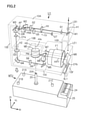
- FIG. 2 is a perspective view showing the detailed configuration of the drawing unit U1 and the arrangement of the inspection tool device MTU as a representative of the drawing units U1 to U6 of the pattern drawing apparatus EX of FIG.
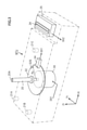
- FIG. 3 is a perspective view showing a main internal configuration of the inspection tool device MTU shown in FIG.
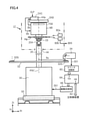
- FIG. 4 is a diagram schematically showing the configurations of various functional members required for measurement when the drawing unit U1 is docked to the inspection tool device MTU shown in FIG. 3 for inspection.
- FIG. 1 is a diagram schematically showing the arrangement of drawing units U1 to U6 mounted on the pattern drawing apparatus EX applied as the first embodiment.
- FIG. 2 is a perspective view showing the detailed configuration of the drawing unit U1 and the arrangement of the inspection tool device MTU as a representative of the drawing units U1 to U6 of the pattern drawing apparatus EX of FIG.
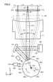
- FIG. 5 is a diagram showing a scanning state of the spot light SP by the polygon mirror PM and the f ⁇ lens system FT in the drawing unit U1 shown in FIG. 2.
- FIG. 6 is a diagram schematically showing how the spot light SP draws a pattern on the substrate P according to the pixel map defined by the drawing data.
- FIG. 7 is a schematic view showing an exaggerated portion of the scale disk 32 in the inspection tool device MTU near the reading center position 34A of the scale 32G by the encoder head 34.
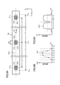
- 8A shows a detailed configuration of the sensor unit unit 24 shown in FIGS. 2 and 3
- FIG. 8B shows an example of the waveform of the detection signal SS2 output from the sensor unit unit 24, and
- FIG. 8C is a diagram.
- FIG. 9 is a graph showing an exaggerated error in the correlation state between the scanning position of the spot light SP by one reflecting surface of the polygon mirror PM and the rotation angle position of the polygon mirror PM.
- FIG. 10A shows a first modification example of a slit opening provided on the detection surface 24A of the sensor unit unit 24 for photoelectric detection of the spot light SP
- FIG. 10B is an example of a waveform obtained from the photodetector DTa
- 10C is a diagram showing an example of a waveform obtained from the photodetector DTb
- FIG. 10D is a diagram showing an example of a waveform obtained from the photodetector DTc.
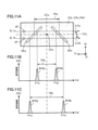
- FIG. 11A shows a second modified example of the slit opening formed in the light-shielding region 24s (24c, 24e) on the detection surface 24A of the sensor unit unit 24, and
- FIG. 11B shows the spot light SP along the drawing line SL1a.
- 11C shows an example of a waveform obtained when the spot light SP moves along the drawing line SL1b
- FIG. 11C shows an example of a waveform obtained when the spot light SP moves along the drawing line SL1b.
- FIG. 11C shows an example of a waveform obtained when the spot light SP moves along the drawing line SL1b.
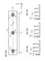
- FIG. 12A shows a fourth modified example of the slit opening formed in the light-shielding regions 24s, 24c, 24e on the detection surface 24A of the sensor unit unit 24, and
- FIG. 12B is an example of the waveform obtained from the photodetector DTa.
- 12C is a diagram showing an example of a waveform obtained from the photodetector DTb
- FIG. 12D is a diagram showing an example of a waveform obtained from the photodetector DTc.
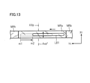
- FIG. 13 is a diagram illustrating a state of the beam LB1 projected on the reflecting surface MRa of the polygon mirror PM (the same applies to the other reflecting surfaces MRb to MRh).
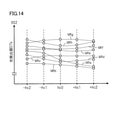
- FIG. 14 exaggerates a measurement example (fifth modification example) in which the change in the illuminance of the spot light SP according to the tilted position of the parallel flat plate HV is obtained for each of the reflective surfaces MRa to MRh of the polygon mirror PM. It is a graph.
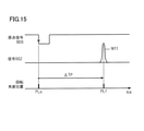
- FIG. 15 shows an example of measuring the difference between the position where the origin signal BDS is generated from the drawing unit U1 and the position where the detection signal SS2 is generated corresponding to the slit opening SSa of the sensor unit unit 24 (9th modification).
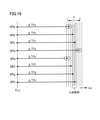
- FIG. 16 is a diagram schematically showing the difference amount for each reflecting surface of the polygon mirror PM obtained by the measurement example of FIG.
- the substrate processing apparatus (pattern forming apparatus) according to the aspect of the present invention will be described in detail below with reference to the attached drawings, with reference to suitable embodiments. It should be noted that the aspects of the present invention are not limited to these embodiments, but include those with various changes or improvements. That is, the components described below include those that can be easily assumed by those skilled in the art and those that are substantially the same, and the components described below can be appropriately combined. In addition, various omissions, substitutions or changes of components can be made without departing from the gist of the present invention.
- FIG. 1 is a diagram showing a schematic configuration of a pattern forming apparatus (pattern drawing apparatus) EX that exposes a pattern to a substrate (irradiated body) P as a substrate processing apparatus according to the first embodiment, and is a basic diagram thereof.
- the structure is the same as that disclosed in International Publication No. 2017/197777, International Publication No. 2018/061633, and International Publication No. 2019/082850.
- an XYZ Cartesian coordinate system with the gravity direction as the Z direction is set, and the X direction, the Y direction, and the Z direction are set according to the arrows shown in the figure.
- the pattern drawing device EX is used in a device manufacturing system that manufactures an electronic device by exposing a fine pattern for an electronic device to a photosensitive functional layer such as a photoresist coated on the substrate P.
- a photosensitive functional layer such as a photoresist coated on the substrate P.
- the substrate P is delivered from a supply roll (not shown) in which a flexible sheet-shaped substrate (sheet substrate) P is wound in a roll shape, and various processes are continuously performed on the sent substrate P.
- the substrate P has a so-called roll-to-roll (Roll To Roll) production method in which the substrate P after various treatments is wound up with a recovery roll (not shown). Therefore, at least on the substrate P being manufactured, a large number of patterns corresponding to the unit device (one display panel, etc.) to be the final product are arranged in a continuous state with a predetermined gap in the transport direction of the substrate P. Will be done.
- the substrate P has a strip shape in which the elongated direction is the moving direction (transporting direction) of the substrate P and the short direction orthogonal to the elongated direction is the width direction of the substrate P.
- the substrate P for example, a resin film, a foil made of a metal such as stainless steel, or a foil made of an alloy is used.
- the material of the resin film include polyethylene resin, polypropylene resin, polyester resin, ethylene vinyl copolymer resin, polyvinyl chloride resin, cellulose resin, polyamide resin, polyimide resin, polycarbonate resin, polystyrene resin, and vinyl acetate resin. Of these, those containing at least one may be used.
- the thickness and rigidity (Young's modulus) of the substrate P are within a range in which the substrate P does not have creases or irreversible wrinkles due to buckling when passing through the transport path of the device manufacturing system or the pattern drawing device EX. If it is good.
- a film such as PET (polyethylene terephthalate), PEN (polyethylene naphthalate), or polyimide having a thickness of about 25 ⁇ m to 200 ⁇ m as a base material of the substrate P is typical of a suitable sheet substrate.
- the substrate P is a single layer of ultrathin glass having a thickness of about 30 to 100 ⁇ m manufactured by a float method or the like, a laminated body in which the above resin film, metal foil or the like is bonded to the ultrathin glass, or A piece of paper containing nanocellulose and having its surface smoothed may be used.
- the photosensitive functional layer applied to the surface of the substrate P is applied as a solution on the substrate P and dried to become a layer (film).
- a typical photosensitive functional layer is a photoresist (liquid or dry film), but as a material that does not require development processing, the photosensitive functional layer is modified in terms of the liquid repellency of the portion exposed to ultraviolet rays.
- SAM silane coupling agent
- a photosensitive reducing agent that exposes a plating-reducing group to a portion irradiated with ultraviolet rays and a photosensitive reducing agent that removes a plating-reducing group from a portion irradiated with ultraviolet rays.
- the pattern portion exposed to ultraviolet rays on the substrate P is modified from liquid repellent to liquid repellent. Therefore, by selectively coating a conductive ink (ink containing conductive nanoparticles such as silver and copper) or a liquid containing a semiconductor material on the portion that has become liquid-friendly, a thin film (TFT) or the like can be used. It is possible to form a pattern layer as a wiring for electrodes, semiconductors, insulation, or connections constituting the above.
- the plating reducing group is exposed on the pattern portion exposed to ultraviolet rays on the substrate P or the unexposed pattern portion. Therefore, after exposure, the pattern layer is formed (precipitated) by electroless plating in which the substrate P is immediately immersed in a plating solution containing palladium ions, copper ions, or the like for a certain period of time.
- a plating process is an additive (addition type) process, but in addition, an etching process as a subtractive (subtraction type) process may be premised.
- the substrate P sent to the pattern drawing apparatus EX uses PET or PEN as the base material, and a metallic thin film such as aluminum (Al) or copper (Cu) is deposited on the entire surface thereof or selectively, and further, the substrate P thereof is deposited. It is assumed that a photoresist layer is laminated on top.
- the pattern drawing device EX shown in FIG. 1 is a direct drawing type exposure device that does not use a mask, a so-called spot scanning type exposure device, and the substrate P conveyed from the process device in the previous process is used as a process device in the subsequent process. It is conveyed in the elongated direction at a predetermined speed toward (including a single processing unit or a plurality of processing units).
- the pattern drawing device EX has one of a signal line constituting an electronic device, a wiring pattern of a power supply line, an electrode constituting a TFT, a semiconductor region, a through hole, etc. in the photosensitive functional layer of the substrate P.
- An optical pattern corresponding to the pattern shape of the above is formed by high-speed scanning in the Y direction (main scanning) of spot light whose intensity is modulated according to drawing data and movement of the substrate P in the long direction (secondary scanning). ..
- the pattern drawing device EX has a pattern for each portion of a rotary drum DR that supports a substrate P for subscanning and conveys it in a long direction, and a portion of the substrate P that is supported in a cylindrical surface by the rotary drum DR.
- a plurality of (here, 6) drawing units Un (U1 to U6) for exposure are provided, and each of the plurality of drawing units Un (U1 to U6) is a spot of a pulsed beam (pulse beam) for exposure.
- the intensity of the spot light is modulated at high speed according to the drawing data. (On / Off).
- an optical pattern corresponding to a predetermined pattern such as an electronic device, a circuit, or a wiring is drawn and exposed on the irradiated surface of the substrate P.
- the pattern forming mechanism is configured by each or all of the six drawing units U1 to U6.
- the rotary drum DR has a central axis AXo extending in the Y direction and a cylindrical outer peripheral surface DRa having a constant radius from the central axis AXo.
- the rotary drum DR rotates around the central axis AXo to lengthen the substrate P while supporting (holding close contact) a part of the substrate P by bending it in a cylindrical surface shape in the elongated direction following the outer peripheral surface DRa. Transport in the scale direction.
- the rotary drum DR supports a region (part) on the substrate P on which the beam LB (spot light) from each of the six drawing units U1 to U6 is projected by its outer peripheral surface DRa.
- shafts Sft supported by the main body of the apparatus via bearings are provided so as to rotate the rotary drum DR around the central axis AXo.
- Rotational torque from a rotational drive source (for example, a motor, a reduction mechanism, etc.) (not shown) is applied to the shaft Sft, and the rotary drum DR rotates at a constant rotational speed around the central axis AXo.
- the odd-numbered drawing units U1, U3, and U5 of the six drawing units U1 to U6 are arranged so as to be arranged in the Y direction on the upstream side in the transport direction of the substrate P, and the even-numbered drawing units U2. , U4 and U6 are arranged so as to line up in the Y direction on the downstream side of the substrate P in the transport direction.
- Each of the six drawing units U1 to U6 has a pulsed beam (oscillated at any frequency in the range of 100 MHz to 400 MHz) LB1 to LB6 from a light source device (pulse light source device) (not shown), for example, internationally.
- a light source device pulse light source device
- the beam from the light source device has a peak wavelength (for example, 405 nm, 365 nm, 355 nm, 344 nm, 308 nm, 248 nm, etc.) in the wavelength band of 410 to 200 nm so as to have sensitivity to the photosensitive functional layer of the substrate P. It is set to ultraviolet light having (center wavelength) of.
- the light source device is amplified by a semiconductor laser element, a fiber amplifier, and a fiber amplifier that generate pulsed light in the infrared wavelength region, as disclosed in, for example, International Publication No. 2015/166910 and International Publication No. 2017/057415.
- the fiber amplifier laser light source is composed of a wavelength conversion element (harmonic generation element) or the like that converts pulsed light in the infrared wavelength range into pulsed light in the ultraviolet wavelength range.
- the pulse generation of the beam can be turned on / off at high speed according to the state of (logical value is "0" or "1").
- the beams LB1 to LB6 emitted from the light source device and incident on each of the drawing units U1 to U6 via the acousto-optic modulation element (AOM) for switching have a beam diameter of about 1 mm or about half of the beam diameter. It is a thin parallel light source.
- the pattern drawing apparatus EX is a multi-head type direct drawing exposure method in which six drawing units U1 to U6 having the same configuration are arranged.
- Each of the drawing units U1 to U6 draws a pattern for each partial region partitioned in the Y direction (main scanning direction) of the substrate P supported by the outer peripheral surface DRa of the rotating drum DR.
- Each of the drawing units U1 to U6 projects each of the beams LB1 to LB6 supplied via the acoustic-optical modulation element for switching onto the substrate P (on the irradiated surface of the substrate P), and at the same time, a predetermined opening. Condensate (converge) with numerical aperture (NA).
- each of the beams LB1 to LB6 projected on the substrate P becomes spot light having a diameter of 2 to 4 ⁇ m.
- the spot light of each of the beams LB1 to LB6 projected on the substrate P is scanned in the main scanning direction (Y direction) by the rotation of the polygon mirrors PM provided in each of the drawing units U1 to U6.
- linear drawing lines (scanning lines) SL1 to SL6 for drawing a pattern for one line are defined on the substrate P.
- the drawing lines SL1 to SL6 by each of the drawing units U1 to U6 sandwich the central plane CPo parallel to the YZ plane including the central axis AXo of the rotary drum DR in the circumferential direction of the rotary drum DR.
- the odd-numbered drawing lines SL1, SL3, and SL5 are located on the upstream side (-X direction side) of the substrate P in the transport direction with respect to the central surface CPo, and are located in the Y direction. They are arranged in a row at predetermined intervals along the line.
- the even-numbered drawing lines SL2, SL4, and SL6 are located on the downstream side (+ X direction side) of the substrate P in the transport direction with respect to the central surface CPo, and are separated by a predetermined interval along the Y direction in one row. Is located in. Therefore, the odd-numbered drawing units U1, U3, and U5 and the even-numbered drawing units U2, U4, and U6 are arranged symmetrically with respect to the central plane CPo when viewed in the XZ plane (viewed from the Y direction). Will be done.
- the six drawing units U1 to U6 have a scanning area (main scanning range section) in the Y direction so as to cover the width direction (Y direction) dimension of the exposure region (pattern forming region) on the substrate P in total. Sharing. For example, assuming that the main scanning range (the length of the drawing line SLn) in the Y direction by one drawing unit Un is about 30 to 60 mm, drawing is possible by arranging the six drawing units U1 to U6 in the Y direction. The width of the exposed area in the Y direction can be expanded to about 180 to 360 mm.
- each of the drawing lines SL1 to SL6 (the length of the drawing range) is the same in principle, that is, the scanning distance of the spot light of the beam LBn scanned along each of the drawing lines SL1 to SL6 is in principle. It is the same as.
- Each of the drawing units U1 to U6 is provided with a telecentric f ⁇ lens system (scanning optical system for drawing) FT that incidents a beam LBn that is reflected by each reflecting surface of the polygon mirror PM and deflected in the main scanning direction, and is an f ⁇ lens.
- Each beam LBn ejected from the system FT and projected onto the substrate P is set to travel toward the central axis AXo of the rotating drum DR when viewed in the XZ plane.
- each of the main rays of the beams LB1 to LB6 traveling from each of the drawing units U1 to U6 toward the substrate P becomes a tangent plane at the position of the drawing line SLn on the curved surface of the substrate P in the XZ plane.
- it is set to always be vertical. That is, each of the beams LB1 to LB6 projected on the substrate P is scanned in a telecentric state with respect to the main scanning direction and the sub-scanning direction (circumferential direction along the outer peripheral surface DRa of the rotating drum DR) of the spot light.
- the substrate P is supported within an angle range of about 180 degrees of the outer peripheral surface DRa of the rotating drum DR.
- the odd-numbered drawing units U1, U3, and U5 are tilted counterclockwise by a certain angle ⁇ c from the central plane CPo, and the even-numbered drawing units U2, U4, The U6 is tilted clockwise from the central surface CPo by a certain angle ⁇ c.
- each of the six drawing units U1 to U6 for example, as disclosed in International Publication No. 2016/152758, each incident center line of the beams LB1 to LB6 incident on each of the drawing units U1 to U6.
- the f ⁇ lens system FT is pivotally supported around the lines LE1 to LE6 coaxial with the optical axes AXf1, AXf2, ....
- a plurality of alignment systems ALGn arranged at predetermined intervals in the Y direction are provided on the upstream side of the pattern drawing positions (drawing lines SL1, SL3, SL5) by each of the odd-numbered drawing units U1, U3, U5, a plurality of alignment systems ALGn arranged at predetermined intervals in the Y direction are provided. Be done.
- the extension line of the optical axis AXs of each objective lens of the alignment system ALGn is set so as to be perpendicular to the surface of the substrate P and toward the central axis AXo of the rotating drum DR, and the central surface CPo of the extension line of the optical axis AXs is set.
- the angle from is set to ⁇ a ( ⁇ a> ⁇ c).
- the polygon mirror PM and f ⁇ lens system FT constituting each of the drawing units U1 to U6, as well as other optical components such as mirrors, lens systems, beam splitters, and electricity such as sensors and motors.
- the components are integrally assembled in a rigid housing frame.
- the housing frame is attached to the apparatus main body column at the positions of lines LE1 to LE6 in FIG. 1 via a rotation shaft mechanism. By disassembling the rotation axis mechanism, each of the drawing units U1 to U6 can be removed from the main body column of the apparatus together with the housing frame.
- FIG. 2 shows the detailed internal configuration of the drawing unit U1 among the drawing units Un (U1 to U6) according to the present embodiment, the rotation angle position of the polygon mirror PM in the drawing unit U1, and the spot light.
- It is a perspective view which shows the arrangement relation of the calibration apparatus (inspection tool apparatus) MTU for confirming the correspondence relation with the scanning position.
- the same members as those shown in FIG. 1 are designated by the same reference numerals, and the coordinate system is the Cartesian coordinate system XtYtZt shown in FIG.
- the arrangement and configuration of the optical members in the drawing unit U1 shown in FIG. 2 are basically disclosed in International Publication No. 2019/08285, and will be briefly described.
- the beam LB1 (parallel luminous flux of linear polarization) transmitted from the acousto-optic modulation element (AOM) for switching is reflected by the mirror M1 inclined at 45 ° parallel to the Zt axis and -Xt parallel to the Xt axis. Go in the direction.
- the beam LB1 reflected by the mirror M1 is converted into a parallel light flux whose beam diameter is expanded by a beam expander by the two lens systems G1 and G2, and passes through the mirror M2, the polarizing beam splitter PBS, and the aperture stop AP, and the mirror M3.
- a parallel flat plate HV made of quartz that can be inclined around the rotation axis Cz parallel to the Zt axis is provided. Due to the inclination of the parallel flat plate HV, the drawing line SL1 on the irradiated surface of the spot light can be finely moved in the Xt direction in the range of several times to ten and several times the diameter of the spot light.
- the beam LB1 reflected by the mirror M3 passes through the 1/4 wave plate ( ⁇ / 4 plate) QW, is converted into circularly polarized light, and is incident on the first cylindrical lens CYa.
- the first cylindrical lens CYa has a bus set parallel to the Yt axis, has a predetermined refractive power (finite focal length) in the Xt direction, and has no refractive power in the Yt direction (focal length is infinite). ) It is a lens.
- the beam LB1 that has passed through the first cylindrical lens CYa is bent by the mirror M4 so as to have an optical path parallel to the Xt axis, travels in the + Xt direction, and is incident on the lens system G4.
- the beam LB1 that has passed through the lens system G4 is reflected by the mirrors M5, M6, and M7 and reaches the reflection surface of the polygon mirror PM.
- the first cylindrical lens CYa converges the beam LB1 only in the Xt direction at a position in front of the lens system G3 (the rear focal position of the first cylindrical lens CYa) and concentrates the beam LB1 in a slit shape extending in the Yt direction. ..
- the two-lens system G3 and G4 function as an imaging system, and the rear focal position of the first cylindrical lens CYa (the position where the beam LB1 condenses in a slit shape) is set on the reflective surface of the polygon mirror PM (here,). It is set to have an optically conjugate relationship with (8 faces).
- the beam LB1 reflected by the reflection surface of the polygon mirror PM has a reflection surface having a length equal to or longer than the drawing line SL1 in the Yt direction after passing through a telecentric f ⁇ lens system FT having an optical axis AXf1 parallel to the Xt axis.
- the beam LB1 reflected by the mirror M8 has a bus set parallel to the Yt axis, has a predetermined refractive power (finite focal length) in the Xt direction, and has no refractive power in the Yt direction (focal length).
- the combination of the first cylindrical lens CYa and the second cylindrical lens CYb corrects the blurring of the drawing line SL1 in the Xt direction due to the tilt error of each reflecting surface of the polygon mirror PM.
- the spot light of the beam LB1 projected on the substrate P or on the outer peripheral surface DRa of the rotary drum DR is a reference formed on the pattern or alignment mark on the substrate P or the outer peripheral surface DRa.
- a lens system G5 for photoelectrically detecting the reflected light generated when the pattern is scanned and a photodetector (photodiode or the like) DT are provided.
- the reflected light (mainly circularly polarized light) from the substrate P or the outer peripheral surface DRa is polarized via the second cylindrical lens CYb, the f ⁇ lens system FT, the polygon mirror PM, the first cylindrical lens CYa, the ⁇ / 4 plate QW, and the like.
- Beam splitter Return to PBS.
- the reflected light is converted into linear polarization transmitted through the polarizing beam splitter PBS by the ⁇ / 4 plate QW, and is focused on the light receiving surface of the photodetector DT by the lens system G5.
- the housing frames of the drawing unit U1 are arranged at predetermined intervals in the Zt direction, and the upper support plate portion 10A and the middle stage are parallel to the XtYt plane, respectively. It has a support plate portion 10B and a lower support plate portion 10C. Further, the housing frame has a support plate 10D connecting the ends of the upper support plate portion 10A and the middle stage support plate portion 10B in the Zt direction on the wire LE1 (rotational axis mechanism of the entire drawing unit U1) side, and the upper stage support plate portion 10A.
- the support plate 10E that integrally connects the ends of the middle support plate portion 10B and the lower support plate portion 10C in the ⁇ Xt direction, and the middle stage support plate portion 10B extending in the ⁇ Zt direction from the end on the line LE1 side. It has a support plate 10F and a support plate 10F.
- a mirror M1, a lens system G1, G2, a parallel flat plate HV, a mirror M2, a polarizing beam splitter PBS, an aperture diaphragm AP, a lens system G5, and an optical detector DT are attached to the upper support plate portion 10A, and acoustic optics for switching is attached.
- the beam LB1 from the modulation element (AOM) is projected onto the mirror M1 through the through hole H1 formed in the upper support plate portion 10A.
- a mirror M3, a ⁇ / 4 plate QW, a first cylindrical lens CYa, a lens system G3, and a mirror M4 are attached to a support plate 10E extending parallel to the YtZt plane, and the beam LB1 from the mirror M3 to the mirror M4 is attached.
- a through hole H2 is formed at a corresponding position of the middle support plate portion 10B so as not to block the optical path.
- a drive circuit board (not shown) with a heat radiating member that supports the motor MD of the polygon mirror PM is attached to the middle support plate portion 10B at the position of the through hole H3, and the mirror M6, the mirror M7, and the f ⁇ lens system FT are attached. It is attached. Further, the lens system G4 and the mirror M5 are attached to the lower support plate portion 10C, and the mirror M8 and the second cylindrical lens CYb are attached to the support plate 10F. Although not shown in FIG. 2, in order to increase the rigidity of the housing frame, the middle support plate portion 10B and the lower support plate portion 10C are placed in the Zt direction on both sides of the f ⁇ lens system FT in the Yt direction.
- a bar member (prism member) to be connected is attached, and a bar member (prism member) is attached between both sides in the Yt direction and the end in the + Xt direction of the lower support plate portion 10C at the end portion on the ⁇ Zt side of the support plate 10F. It is attached.
- a through hole H4 is formed in the lower support plate portion 10C as a housing frame at a position in the XtYt plane corresponding to the central axis AXp of rotation of the polygon mirror PM (motor MD). Has been done.
- the through hole H4 is provided to pass the rotary shaft 20 extending in the + Zt direction from the inspection tool device MTU.
- the drawing unit U1 (lower support plate portion 10C) to be inspected can be detachably mounted in the Zt direction on the upper surface portion of the inspection tool device MTU parallel to the XtYt plane.
- the scanning position of the spot light and the intensity of the spot light are located at the position of the drawing line SL1 by scanning the spot light of the beam LB1 projected from the second cylindrical lens CYb of the drawing unit U1.
- a sensor unit portion 24 for measuring and the like is attached via a mount member 25.
- FIG. 3 is a perspective view showing the configuration of the main part inside the inspection tool device MTU shown in FIG. 2, and the rotary shaft 20 includes a servomotor 30 for rotational drive and a scale disk 32 for encoder measurement. It is mounted coaxially.
- the servomotor 30 may be composed of a torque motor with a reduction gear mechanism or a step motor capable of step rotation at a minute unit angle.
- the servo motor 30 has a characteristic that the rotation angle position can be set with high accuracy (a characteristic that can be stationary at the target rotation angle position). It suffices to have it, and it is not necessary to rotate it at high speed.
- the scale disk 32 will be described in detail later, one having a diameter as large as possible is selected in order to improve the measurement resolution, and the scale disk 32 is engraved at a constant pitch in the circumferential direction in a ring-shaped region having a radius Rs near the outer circumference of the scale disk 32. It has a grid scale of 32G.
- the optical encoder head 34 arranged to face the grid scale (hereinafter, also simply referred to as a scale) 32G outputs a measurement signal SS1 according to a change in the position of the scale 32G in the circumferential direction.
- the measurement signal SS1 is a sinusoidal or rectangular wave two-phase signal whose phase is shifted by 90 °, or a signal for heterodyne detection (FM demodulation) whose frequency (phase) shifts from the reference frequency as the scale 32G moves. Generated.
- the sensor unit unit 24 is interchangeably attached to the mount member 25 having a different sensing method, and outputs the detection signal SS2.
- the sensor unit unit 24 includes a one-dimensional or two-dimensional image pickup element in which a large number of pixels are arranged in the Yt direction along the drawing line SL1, a scanning start position, a scanning end position, and a scanning end position of spot light on the drawing line SL1.
- a transmission slit having a line width equal to the size (diameter) of the spot light or several times the size of the spot diameter is arranged, and the amount of transmitted light of the transmission slit is detected. It can be a diode or the like.
- the drawing unit U1 (the same applies to the other drawing units U2 to U6) is removed from the main body of the pattern drawing apparatus EX and mounted on the inspection tool apparatus MTU, the pattern drawing is performed. It is difficult to guide the beam from the light source device mounted on the device EX as the beam LB1. Therefore, in order to project the beam LB1 (parallel luminous flux with a diameter of 0.5 to 1 mm) toward the mirror M1 in the desired state, another light source device and an acousto-optic modulation element (AOM) for switching are provided.
- the beam transmission optical system is positioned and installed with respect to the inspection tool device MTU.
- an adjustment docking mechanism for confirming the optical characteristics of the drawing unit Un (U1 to U6) alone is provided in the pattern drawing apparatus EX. If it is provided, the drawing unit U1 mounted on the inspection tool device MTU is arranged therein so that the beam from the light source device mounted on the pattern drawing device EX is incident on the mirror M1 of the drawing unit U1. You can do it.
- FIG. 4 is a diagram schematically showing the configuration of various functional members required for measurement when inspecting the drawing unit U1 docked to the inspection tool device MTU.
- the origin for detecting the moment when each of the reflective surfaces of the polygon mirror PM reaches a predetermined rotation angle position in the drawing unit U1 (the same applies to the other drawing units U2 to U6).
- a sensor unit is provided.
- the origin sensor unit is reflected by the light source unit BDa by a semiconductor laser, a light emitting diode, etc., which projects a measurement beam having a long wavelength different from that of the drawing beam LB1 onto the reflection surface of the polygon mirror PM, and each reflection surface of the polygon mirror PM.
- It is composed of a light receiving unit BDb that receives the measured beam and outputs a pulsed origin signal BDS.
- the arrangement of the light source unit BDa and the light receiving unit BDb of the origin sensor unit is disclosed in, for example, International Publication No. 2018/061633.
- a generator FGS that outputs a sinusoidal or rectangular wave speed signal Se whose frequency changes in proportion to a change in rotation speed is provided.
- the motor MD is attached to a drive circuit board CKB with a heat dissipation member (heat dissipation fin), and the drive circuit board CKB has a clock signal CLP having a frequency corresponding to the target rotation speed sent from the main control circuit and a generator FGS.
- a drive circuit DVC that outputs a drive signal (current adjustment signal) Sm for rotating the motor MD by the PLL method is provided.
- a contact CS is provided coaxially with the rotation center axis AXp.
- the contact CS is in close contact with the contact portion 20A at the tip of the rotary shaft 20 of the inspection tool device MTU so as to be coaxial with the contact portion 20A.
- the rotary shaft 20 is in a state where the supply of the drive signal Sm by the drive circuit DVC is stopped, the motor MD (polygon mirror PM) is in a state where it can freely rotate, and the contact portion 20A is in close contact (friction coupling) with the contact CS.
- the polygon mirror PM (motor MD) When the polygon mirror PM (motor MD) is rotated at a low speed, the polygon mirror PM (motor MD) rotates at the same angular velocity as the rotating shaft 20 rotates.
- the contact portion 20A of the rotating shaft 20 is formed in a hemispherical shape and is urged in the + Zt direction by an elastic member (spring).
- the contact CS is formed in a conical recess that fits with the hemisphere of the contact portion 20A.
- a fine movement stage mechanism that integrally moves the servomotor 30 (and the scale disk 32) and the encoder head 34 in a plane parallel to the XtYt plane in two dimensions (within ⁇ several mm). 50 is provided.
- the fine movement stage mechanism 50 moves the contact portion 20A of the rotary shaft 20 on the order of ⁇ m by a micrometer head or the like, and rotates with the central axis AXp of the contact CS on the drawing unit U1 side docked to the inspection tool device MTU. It is used to make fine adjustments so that the central axis AXp'of rotation of the shaft 20 (contact portion 20A) is precisely coaxial.
- a counter circuit unit that outputs a digital value of the movement position (rotation angle position) or movement amount in the circumferential direction of the grid scale 32G of the scale disk 32 based on the measurement signal SS1 from the encoder head 34.
- a servo control circuit unit 64 for inputting the information Icb of the above, and a drive circuit unit 66 for rotationally driving the servomotor 30 by feedback control so that the information Ica matches the information Icb are provided.
- the servomotor 30 is rotated by the drive signal DS1 output from the drive circuit unit 66.
- the drawing unit U1 is docked to the inspection tool device MTU, the contact portion 20A of the rotating shaft 20 and the contact CS of the polygon mirror PM are coaxially fitted, and then the beam LB1 is directed toward the mirror M1 of the drawing unit U1. Is incident.
- the light source device is a fiber amplifier laser light source
- the beam LB1 is supplied in a mode in which pulsed light is continuously emitted at a predetermined oscillation frequency.
- the drive circuit board CKB and the drive circuit DVC for rotating the motor MD in the drawing unit U1 are energized and the motor MD is in a rotatable state, the supply of the drive signal Sm is controlled to be stopped. ..
- the correspondence between the rotation angle position of the polygon mirror PM of the drawing unit U1 and the scanning position of the spot light of the beam LB1 for drawing on the drawing line SL1 is the measurement signal SS1 from the encoder head 34 of the inspection tool device MTU, that is, The inspection is performed based on the information Ica of the actual rotation angle position of the scale disk 32 output from the counter circuit unit 60 and the detection signal SS2 output from the sensor unit unit 24. Therefore, with reference to FIGS. 5 and 6, the conditions of the scale disk 32 for obtaining the correspondence between the rotation angle position of the polygon mirror PM and the scanning position of the spot light with high accuracy (high resolution) will be described. ..
- FIG. 5 is a view of the scanning state of the spot light SP by the polygon mirror PM and the f ⁇ lens system FT in the drawing unit U1 shown in FIG. 2 in the XtYt plane
- FIG. 6 is a diagram showing pixels defined by drawing data. It is a figure which schematically represented how the spot light SP draws a pattern on a substrate P according to a map.
- the Cartesian coordinate system XtYtZt is set to be the same as in FIG. 2, and the same members as those in FIG. 2 are designated by the same reference numerals.
- FIG. 5 the Cartesian coordinate system XtYtZt is set to be the same as in FIG. 2, and the same members as those in FIG. 2 are designated by the same reference numerals.
- the mirror M8 arranged immediately after the f ⁇ lens system FT is omitted, and the optical axis AXf1 of the f ⁇ lens system FT is shown to go straight and pass through the second cylindrical lens CYb.
- the spot light SP of the beam LB1 emitted from the second cylindrical lens CYb is located on the detection surface (image surface corresponding to the surface of the substrate P) 24A of the sensor unit unit 24 in the depth of focus DOF (Depth of Focus). It is assumed that the light is focused.
- the polygon mirror PM of the present embodiment has eight reflecting surfaces MRa, MRb, MRc, MRd, MRe, MRf, MRg, and MRh, and is assumed to rotate clockwise in the XtYt plane.
- the beam LB1 reflected in the + Yt direction by the mirror M6 in the drawing unit U1 shown in FIG. 2 is reflected by the mirror M7 and is incident on the reflection surface MRa of the polygon mirror PM.
- the mirror M7 is arranged so that the main ray at the center of the beam LB1 reflected by the mirror M7 and the optical axis AXf1 of the f ⁇ lens system FT form 45 ° in the XtYt plane. Further, in FIG.
- the reflection surface MRa of the polygon mirror PM is tilted by 22.5 ° (45 ° / 2) in the XtYt plane with respect to the plane perpendicular to the optical axis AXf1 of the f ⁇ lens system FT.
- the main ray at the center of the beam LB1 reflected by the reflecting surface MRa represents the moment) and is substantially coaxial with the optical axis AXf1.
- the beam LB1 passing through the f ⁇ lens system FT and the second cylindrical lens CYb is focused as a spot light SP at a position on the detection surface 24A through which the optical axis AXf1 passes.
- the measurement beam from the light source unit BDa as the origin sensor unit is projected onto the reflection surface MRb immediately before the reflection surface MRa in the rotation direction of the polygon mirror PM, and the light receiving unit BDb receives the reflected beam. Due to the rotation of the polygon mirror PM, the light receiving unit BDb receives the reflected beam of the measurement beam at a certain time before the moment when the spot light SP of the beam LB1 passes through the scanning start position PLs on the detection surface 24A. Then, the pulsed origin signal BDS is output.
- the main ray at the center of the beam LB1 incident on the f ⁇ lens system FT is It is deflected in an angle range (2 ⁇ s) from ⁇ s to + ⁇ s with respect to the optical axis AXf1 of the f ⁇ lens system FT. Due to the deflection of the beam LB1 in the angle range 2 ⁇ s, the spot light SP on the detection surface 24A is scanned from the scanning start position PLs to the scanning end position PLe.
- the distance from the midpoint to the scanning start position PLs and the distance from the midpoint to the scanning end position PLe are both LYs.
- the maximum scanning length of the spot light SP by the drawing unit U1 (the same applies to the other drawing units U2 to U6) in the main scanning direction (Yt direction) is 2LYs, and the maximum scanning length is 2LYs.
- the rotation angle (scanning contribution angle) of the polygon mirror PM corresponding to is ⁇ v.
- Nr the number of reflective surfaces of the polygon mirror PM
- Nr the number of reflective surfaces of the polygon mirror PM corresponding to one reflective surface
- ⁇ v ⁇ mr Since there is a limitation due to the angle of view (2 ⁇ s) of the beam LB1 that can be incident on the f ⁇ lens system FT, it is usually set to ⁇ v ⁇ mr.
- the ratio ⁇ v / ⁇ mr is called scanning efficiency ⁇ ( ⁇ ⁇ 1), and ⁇ is set to about 1/2 to 1/3.
- FIG. 6 schematically shows a part of the pattern drawn on the substrate P by the spot light SP described with reference to FIG. 5, assuming that the surface of the substrate P is along the XtYt plane of the Cartesian coordinate system. show.
- the Xt direction is the sub-scanning direction (moving direction of the substrate P)
- the Yt direction is the main scanning direction
- the spot light SP moves one-dimensionally in the ⁇ Yt direction.
- a square area whose dimension in the Xt direction is defined by Pux and whose dimension in the Yt direction is defined by Puy is one pixel Pix set on the drawing data.
- the drawing data is a set of bit data (logical values "0" or "1") instructing whether or not to project the spot light SP onto the substrate P for each pixel Pix.
- the dimensions of the pixel Pix (Pux, Puy) and the dimensions of the spot light SP ⁇ sp (diameter corresponding to the intensity of 1/2 or 1 / e 2 of the peak intensity) are set to be about the same, but the dimensions of the pixel Pix are set to the same level.
- the diagonal length dimension and the spot light SP dimension ⁇ sp may be set to the same degree.
- the pixel data has a logical value of "1" during the main scanning of the spot light SP, one pulse of the beam LB1 from the light source device is projected onto the substrate P as in the black spot ONP, and the pixel data has a logical value of "0".
- switching is performed at high speed on the light source device (fiber amplifier laser light source) side so that one pulse of the beam LB1 from the light source device is not projected on the substrate P as in the white dot OFP.
- the pattern drawing apparatus EX drawing units U1 to U6 in the present embodiment, a pattern drawing is performed by projecting two pulses of spot light SP in each of the Xt direction and the Yt direction on one pixel Pix. Therefore, every time the spot light SP moves by Pay / 2 in the Yt direction (main scanning direction), it is switched between an on state such as a black point ONP and an off state such as a white point OFP based on the pixel data.
- the substrate P has a distance Lux / 2 in the Xt direction. Is set to move only. Therefore, one pixel Pix whose pixel data is set to the logical value "1" is exposed by four pulses of the spot light SP.
- the pattern CHP surrounded by the diagonal line defined by the 3 ⁇ 3 pixel Pix shown in FIG. 6 is drawn as a 6 ⁇ m square. Ru.
- the resolution of the encoder measurement by the scale disk 32 in the inspection tool device MTU, the diameter of the scale disk 32, the grid pitch of the scale 32G, and the like are set.
- the maximum scanning length 2LYs of the spot light SP by the drawing unit U1 and the dimension Puy in the main scanning direction (Yt direction) of the pixel Pix the maximum drawing possible during one scanning by one reflecting surface of the polygon mirror PM.
- FIG. 7 is a schematic view showing an exaggerated portion of the scale disk 32 seen in the XtYt plane near the reading center position 34A of the scale 32G by the encoder head 34.
- the counter circuit unit 60 in FIG. 4 is one of 1/8, 1/16, 1/32, 1/64, and 1/128 of the actual lattice pitch of the scale 32G based on the measurement signal SS1. It is equipped with an interpolation processing unit that digitally counts with resolution.
- the interpolation magnification of the interpolation process is Ke (any of 8, 16, 32, 64, 128).
- the interpolation magnification Ke may be an integer.
- the perimeter distance (arc length) on the radius Rs corresponding to the rotation angle ⁇ v is based on the radius Rs of the reading center position 34A by the encoder head 34 on the scale 32G of the scale disk 32.
- ⁇ Gp 2 ⁇ ⁇ Rs ⁇ Ke ⁇ ( ⁇ / Nr) / (e ⁇ Npp) ⁇ ⁇ ⁇ (1)
- the practical lattice pitch ⁇ Gp that can guarantee the accuracy in fabrication is 16 ⁇ m to 20 ⁇ m
- the radius Rs of the scale 32G of the scale disk 32 is about 54 mm to 68 mm (108 mm to 136 mm in diameter). Therefore, the maximum outer diameter (diameter) of the scale disk 32 is about 120 mm to 150 mm, which is a size that can be easily manufactured as the scale disk 32.
- the scale 32G is a scale disk formed along the circumferential direction of the outer peripheral surface parallel to the central axis AXp'(Zt axis) of the scale disk 32, and the reading center position 34A of the encoder head 34 is parallel to the Zt axis. Scale Set on the tangent plane of the outer peripheral surface of the disk.
- the radius of the maximum outer diameter of the scale disk 32 always coincides with the radius Rs in the equation (1). Therefore, even if the reading center position 34A of the encoder head 34 is arranged on the scale 32G with a slight error in the line direction (Zt direction) of the grid, the desired value of the unit angle ⁇ g is maintained.
- the rotation angle position of the polygon mirror PM can be determined with extremely high resolution, specifically, the pulse emission (white point OFP) in FIG. , Black point ONP) can be measured with a pitch Pay / 2 (or 1/2 of the pitch Pay / 4) in the Yt direction.
- the information Ica of the rotation angle position measured by the counter circuit unit 60 shown in FIG. 4 is also sent to the main control device via the interface unit 62.
- the inspection by the encoder measurement system is performed in cooperation with the sensor unit unit 24 shown in FIGS. 2 and 3 or the photodetector DT in the drawing unit U1 (same for U2 to U6) shown in FIG. .. Therefore, the sensor unit unit 24 will be described below with reference to FIGS. 8A to 8C.
- FIG. 8A shows a detailed configuration of the configuration of the sensor unit unit 24 in the XtYt plane
- FIG. 8B shows an example of the waveform of the detection signal SS2 output from the sensor unit unit 24
- FIG. 8C shows FIG. 2
- An example of the waveform of the signal from the photodetector DT in the drawing unit U1 shown in the above is shown.
- the detection surface 24A of the sensor unit unit 24 parallel to the XtYt surface is composed of the surface of a transmission plate made of quartz or the like.
- rectangular light-shielding regions 24s, 24c, and 24e formed of a reflective chromium layer are formed at each of the three locations along the main scanning direction (Yt direction) of the spot light SP.
- Slit openings SSa, SSb, and SSc are formed in each of the light-shielding regions 24s, 24c, and 24e, which are elongated in the Xt direction and whose width in the Yt direction is substantially equal to the dimension (diameter) ⁇ sp of the spot light SP.
- the opening SSa is formed at a position of a distance (interval) LJs in the + Yt direction from the center position YJo, and the slit opening SSc of the light shielding region 24e is formed at a position of a distance (interval) LJs in the ⁇ Yt direction from the center position YJo.
- each of the light-shielding regions 24s, 24c, and 24e receives the spot light SP transmitted through each of the slit openings SSa, SSb, and SSc, and a photoelectric signal corresponding to the light intensity thereof is received.
- the photodetectors DTa, DTb, and DTc that output the light are arranged.
- an amplifier circuit for amplifying the photoelectric signals from each of the photodetectors DTa, DTb, and DTc, and the intensity of the amplified photoelectric signal are converted into digital values in the above figure.
- An AD conversion circuit or the like that outputs as the detection signal SS2 shown in 3 is incorporated.
- each of the light-shielding regions 24s, 24c, and 24e is considered to be inspected using a signal from the photodetector DT (see FIG. 2) provided in the drawing unit U1 (the same applies to U2 to U6). Then, it is formed with a width WS in the Yt direction.
- the width WS is set to be three times or more the width of the slit openings SSa, SSb, SSc, and the spot light SP is other than the slit openings SSa, SSb, SSc on the surfaces of the light-shielding regions 24s, 24c, 24e of the width WS.
- the reflected light generated when projected onto the portion is detected by the photodetector DT in the drawing unit U1 (same for U2 to U6).
- the reflectance with respect to the spot light SP is set to be sufficiently small (for example, 10% or less).
- the polygon mirror PM is rotated by a minute angle (for example, ⁇ g) by the servomotor 30 shown in FIG. 4, and the spot light SP is moved so as to cross the slit opening SSa of the sensor unit unit 24, for example.
- a minute angle for example, ⁇ g
- the spot light SP is moved so as to cross the slit opening SSa of the sensor unit unit 24, for example.
- the vertical axis represents the intensity of the detection signal SS2
- the horizontal axis represents the minimum resolution (least significant bit) of the information Ica of the rotation angle position of the scale disk 32 (that is, the polygon mirror PM) output from the counter circuit unit 60. Represents the positions Y1, Y2, ..., Y8 represented by).
- the rotation of the servomotor 30 is controlled so that the information Ica output from the counter circuit unit 60 coincides with each of the positions Y1, Y2, ..., Y8 only for a certain measurement time.
- the pulsed light of the beam LB1 is supplied to the drawing unit U1 by a predetermined number of pulses, and the detection signal SS2 output from the photodetector DTa during that time is supplied.
- the intensity value (average intensity value due to a large number of pulsed lights) and the position Y1 are sent to the main control device.
- the servomotor 30 is controlled so that the information Ica from the counter circuit unit 60 coincides with the position Y2, and similarly, the intensity value of the detection signal SS2 output from the photodetector DTa and the position Y2 are mainly controlled. Sent to the device.
- the intensity value of the detection signal SS2 is sampled at each of the positions Y3 to Y8.
- the waveform Wf1 is obtained by fitting the intensity value of the detection signal SS2 sampled at each of the positions Y1 to Y8.
- the practical lattice pitch ⁇ Gp of the scale 32G of the scale disk 32 is 16 ⁇ m to 20 ⁇ m
- the radius Rs of the scale 32G is 54 mm to 68 mm
- the interpolation magnification Ke in the counter circuit unit 60 By setting 128, the minimum resolution (unit angle ⁇ g) when measuring the rotation angle of the polygon mirror PM can be set to Puy / 4, which is the minimum movement amount of the spot light SP in the Yt direction. Therefore, in the case of FIG. 8B, the distance (dimension) for one scale from the positions Y1 to Y8 is 1/4 of the dimension Puy of one pixel Pix, that is, about 1/4 of the dimension ⁇ sp of the spot light. ..
- the waveform Wf1 as shown in FIG. 8B is similarly measured based on the detection signals SS2 from each of the other photodetectors DTb and DTc and the information Ica of the rotation angle position from the counter circuit unit 60.
- each of the slit openings SSa, SSb, and SSc is precisely arranged at intervals LJs (LJs ⁇ LYs) in the Yt direction.
- LJs intervals
- the center position of each of the slit openings SSa, SSb, and SSc in the Yt direction is precisely specified within the measurement domain (rotation angle position information Ica) by the encoder measurement system.
- the servomotor 30 (polygon mirror PM) is rotated at a low speed, and the spot light SP continuously pulsed is moved so as to cross each of the light-shielding regions 24s, 24c, and 24e of the sensor unit unit 24.
- the waveform Wf2 due to the change in the intensity of the detection signal output from the photodetector DT in the drawing unit U1 is represented.
- the vertical axis represents the intensity of the detection signal from the photodetector DT
- the horizontal axis represents the information Ica of the rotation angle position of the scale disk 32 (that is, the polygon mirror PM) output from the counter circuit unit 60.
- Each of the light-shielding regions 24s, 24c, and 24e has a relatively high reflectance (for example, 50% or more) in the wavelength region of the beam LB1. Therefore, when the spot light SP moves across each of the light-shielding regions 24s, 24c, and 24e, the reflected light reflected by the portion other than the slit openings SSa, SSb, and SSc is received by the photodetector DT.
- the detection signal has a mid-cracked waveform Wf2 as shown in FIG. 8C.
- the intensity value of the detection signal (waveform Wf2) from the photodetector DT is digitally sampled by an AD conversion circuit (not shown) in response to a change in the information Ica from the counter circuit unit 60.
- the center position of each of the slit openings SSa, SSb, and SSc in the Yt direction is precisely specified within the measurement domain (rotation angle position information Ica) by the encoder measurement system.
- the center of the spot light SP coincides with the center of each of the slit openings SSa, SSb, and SSc of the sensor unit unit 24 based on the information Ica from the counter circuit unit 60. Since the position in the Yt direction can be specified, the correlation state between the scanning position on the detection surface 24A of the spot light SP scanned by the rotation of the polygon mirror PM shown in FIG. 5 and the rotation angle of the polygon mirror PM is shown in FIG. It can be confirmed (inspected) for each of the reflective surfaces MRa to MRh of the polygon mirror PM shown in 1.
- FIG. 9 exaggerates the correlation state between the scanning position of the spot light SP by the reflecting surface MRa of one of the eight reflecting surfaces MRa to MRh of the polygon mirror PM, for example, and the rotation angle position of the polygon mirror PM.
- the vertical axis represents the information Ica from the counter circuit unit 60
- the horizontal axis represents the position YJs of the slit opening SSa, the center position YJo, and the position YJe of the slit opening SSc in the Yt direction. It is assumed that the positions YJs and the positions YJe are precisely arranged at the interval LJs with respect to the center position YJo.
- each of the position YJs, the center position YJo, and the position YJe conforms to the ideal linear characteristic FM. Therefore, it is measured as rotation angle positions ICs, ICo, and ICe specified from the information Ica.
- the linear characteristic FM will be slightly distorted like the characteristic Fma. That is, with reference to the position YJs of the scanning start portion of the spot light SP, at the center position YJo of the scanning center portion, the rotation angle position ICo'with an error of ⁇ o with respect to the ideal rotation angle position ICo is set. At the position YJe of the scanning end portion, the measurement is performed as the rotation angle position ICe'with an error of + ⁇ e with respect to the ideal rotation angle position ICe.
- the characteristic Fma of FIG. 9 is the processing error of the reflective surface of the polygon mirror PM or the residual distortion of the f ⁇ lens system FT in the drawing unit U1 even if the polygon mirror PM is rotated at a constant velocity. It means that a slight error occurs in the constant velocity property in one scan of the spot light SP due to (error from ideal f ⁇ characteristic) and the like. Since the characteristic Fma of FIG. 9 shows a different tendency in each of the reflective surfaces MRa to MRH of the polygon mirror PM, the characteristic Fma as shown in FIG. 9 is acquired for each of the reflective surfaces MRa to MRH using the inspection tool device MTU. ..
- a slight error in the constant velocity of the spot light SP such as the characteristic Fma appears as a partial (local) magnification error in the Yt direction when drawing a pattern, or an overall magnification error.
- the light source device fiber amplifier laser light source
- the characteristic Fma for each reflective surface of the polygon mirror PM can be known, so that the pattern drawing (spot scanning) is performed on which reflective surface of the polygon mirror PM is based on the flag. Therefore, it is possible to correct the error of the drawing magnification due to the characteristic Fma for each reflective surface of the polygon mirror PM on the order of microns.
- the flags for specifying the reflective surface of the polygon mirror PM are, for example, one pulse of the detection signal and one pulse of the detection signal using a rotation detection sensor that generates a detection signal of one pulse for each rotation of the polygon mirror PM, and FIG.
- the error due to the residual distortion aberration (error from the ideal f ⁇ characteristic) in the Yt direction of the f ⁇ lens system FT is commonly included in the characteristic Fma for each reflecting surface of the polygon mirror PM.
- FIG. 10A shows a modified example of the slit opening provided on the detection surface 24A of the sensor unit unit 24 for photoelectric detection of the spot light SP, and shows the members and dimensions constituting the sensor unit unit 24 shown in FIG. 8A above.
- the light-shielding region 24s arranged near the scanning start position PLs is formed elongated in the Yt direction together with the same slit opening SSa as in FIG. 8A, and the width in the Xt direction is the dimension (diameter) ⁇ sp of the spot light SP.
- Slit openings SXs substantially equal to are formed.
- the slit opening SSa and the slit opening SXs are formed at a predetermined interval in the Yt direction.
- the light-shielding region 24e arranged near the scanning end position PLe is formed elongated in the Yt direction together with the same slit opening SSc as in FIG. 8A, and the width in the Xt direction is the dimension (diameter) ⁇ sp of the spot light SP.
- Approximately equal slit openings SXe are formed.
- the slit opening SSc and the slit opening SXe are formed at a predetermined interval in the Yt direction.
- three slit openings SSb shown in FIG. 8A are formed in a constant space in the Yt direction.
- the number of slit openings SSb is not limited to three, and a plurality of slit openings SSb are formed in a line and space shape.
- the slit opening SXs and the slit opening SXe are arranged on a straight line parallel to the Yt axis.
- a photodetector DTa similar to that shown in FIG. 8A is provided in the lower part of the light-shielding region 24s, and the photodetector DTa outputs a photoelectric signal according to the light intensity of the spot light SP transmitted through the slit opening SSa or the slit opening SXs. ..
- a photodetector DTb similar to that shown in FIG. 8A is provided in the lower part of the light-shielding region 24c, and the photodetector DTb outputs a photoelectric signal according to the light intensity of the spot light SP transmitted through each of the plurality of slit openings SSb. do.
- the photodetector DTc outputs a photoelectric signal according to the light intensity of the spot light SP transmitted through the slit opening SSc or the slit opening SXe. ..
- the spot light SP Due to the change in the angle of one reflective surface (for example, the reflective surface MRa) of the polygon mirror PM due to the rotation of the servomotor 30, the spot light SP is turned on as in the black spot ONP (FIG. 6) and is on the light-shielding region 24s in the Yt direction.
- the intensity of the photoelectric signal (detection signal SS2) from the photodetector DTa changes as in the waveforms Wf3a and Wf3b shown in FIG. 10B.
- the horizontal axis represents the information Ica of the rotation angle position output from the counter circuit unit 60 of the encoder measurement system
- the vertical axis represents the intensity of the photoelectric signal from the photodetector DTa.
- the waveform Wf3a in FIG. 10B is the same as the waveform Wf1 shown in FIG. 8B above, and the waveform Wf3b in FIG. 10B is a waveform obtained when the spot light SP accurately moves on the slit opening SXs. be.
- the drawing unit U1 (or any of U2 to U6) is mounted on the inspection tool device MTU,
- the position in the Xt direction on the detection surface 24A of the spot light SP does not always coincide with the position in the Xt direction of the slit openings SXs. Therefore, when the sensor unit unit 24 of FIG. 10A is used, the rotation of the servomotor 30 is controlled so that the spot light SP repeatedly moves on the light-shielding region 24s a plurality of times as an initial setting.
- the amount of inclination of the parallel plate HV in the drawing unit U1 shown in FIG. 2 is increased so that the level of the waveform Wf3b is maximized while monitoring the intensity of the photoelectric signal (detection signal SS2) from the photodetector DTa. Is gradually changed, and the drawing line SL1 is slightly moved in the ⁇ Xt direction to adjust the position.
- the intensity of the photoelectric signal (detection signal SS2) from the photodetector DTc is measured.
- the horizontal axis represents the information Ica of the rotation angle position output from the counter circuit unit 60 of the encoder measurement system
- the vertical axis represents the intensity of the photoelectric signal from the photodetector DTc.
- the waveform Wf5a in FIG. 10D is the same as the waveform Wf1 shown in FIG. 8B above, and the waveform Wf5b in FIG. 10D is a waveform obtained when the spot light SP accurately moves on the slit opening SXe. be.
- the waveform Wf5b may be leveled down like the waveform Wf5b', or the waveform Wf5b' itself may not be obtained.
- the mount member 25 shown in FIGS. 2 and 3 is provided with a sensor fine movement mechanism that slightly rotates the entire sensor unit portion 24 around an axis line parallel to the Zt axis passing through the center of the light-shielding region 24s, and has a slit.
- the relative inclination of the line segment connecting the opening SXs and the slit opening SXe and the drawing line SL1 is corrected.
- the rotation of the servomotor 30 is controlled so that the spot light SP repeatedly moves on the light-shielding region 24e a plurality of times.
- the sensor unit unit is operated by the sensor fine movement mechanism of the mount member 25 until the level of the waveform Wf5b'is maximized like the waveform Wf5b.
- the inclination of 24 is gradually changed to adjust the position.
- the photodetector DTb of FIG. 10A outputs a photoelectric signal (detection signal SS2) having the waveform Wf4 shown in FIG. 10C.
- the horizontal axis represents the information Ica of the rotation angle position output from the counter circuit unit 60 of the encoder measurement system
- the vertical axis represents the intensity of the photoelectric signal from the photodetector DTb.
- the waveform Wf4 in FIG. 10C is the same as the waveform Wf1 shown in FIG. 8B above, and corresponds to each of the three slit openings SSb at three positions along the direction of the position information Icb. It occurs in each.
- the center position YJo is specified in the measurement coordinate system by the encoder measurement system.
- the slit openings SSa, SSb, SSc (and the photodetectors DTa, DTb, DTc) of the sensor unit portion 24 are used for each reflection surface of the polygon mirror PM as shown in FIG.
- the inclination of the drawing line SL1 on the detection surface 24A of the sensor unit unit 24 is made substantially zero. be able to. Therefore, the error measurement of the correlation state between the rotation angle position of the polygon mirror PM and the scanning position of the spot light SP is performed more accurately.
- FIG. 11A is a diagram showing a modified example of the slit opening formed in the light-shielding region 24s (same for 24c and 24e) on the detection surface 24A of the sensor unit unit 24.
- the coordinate system XtYtZt is set in the same manner as in FIG. 10A, and the light-shielding regions 24s (and 24c, 24e) in FIG. 11A are formed at three locations along the Yt direction on the detection surface 24A, as in FIG. 10A. Will be done.
- the drawing line SL1 by the rotation of the polygon mirror PM of the spot light SP and the Yt set on the detection surface 24A of the sensor unit unit 24 are set.
- the axis may be tilted relatively slightly.
- the slit openings SXs and SXe parallel to the Yt axis are provided in FIG. 10A, but in this modification, the Xt axis is provided on the detection surface 24A (XtYt surface).
- a pair of slit openings SKa and SKb tilted 45 ° in the opposite direction to each of the Yt axes are formed in each of the light-shielding regions 24s, 24c and 24e.
- the pair of slit openings SKa, SKb are arranged line-symmetrically with respect to the center line CCx parallel to the Xt axis through the center point CCo on the light-shielding region 24s (and 24c, 24e). Therefore, the extension lines of the slit openings SKa and SKb intersect at 90 °.
- the line passing through the center point CCo and parallel to the Yt axis is the center line CCy
- the distance between the center points in the longitudinal direction of each of the slit openings SKa and SKb in the Yt direction is set to YRo.
- the relative inclination amount between the drawing line SL1 of the spot light SP by the drawing unit U1 and the Yt axis on the sensor unit 24 side is unknown, so the spot light SP is rotated by the rotation of the polygon mirror PM by the servomotor 30.
- the photodetector DTa arranged below the light-shielding region 24s outputs a photoelectric signal (detection signal SS2) as shown in FIG. 11B or FIG. 11C.
- the horizontal axis represents the information Ica of the rotation angle position output from the counter circuit unit 60 of the encoder measurement system
- the vertical axis represents the signal strength of the detection signal SS2.
- the detection signal SS2 peaks at the position PYc where the slit opening SKa and the drawing line SL1b intersect, as shown in FIG. 11C.
- the waveform Wf6a and the waveform Wf6b that peaks at the position PYd where the slit opening SKb and the drawing line SL1b intersect are generated.
- ⁇ Xb (YRo ⁇ YRb) / 2.
- the crossing angle formed by the extension lines of the slit openings SKa and SKb shown in FIG. 11A is not limited to 90 °, and can be any known angle (for example, 60 °, 120 °, 150 °, etc.).
- the amount of inclination of the parallel flat plate HV is changed by a unit amount, and the drawing is performed by a pair of slit openings SKa and SKb and a photodetector DTb formed in the central light-shielding region 24c of the sensor unit unit 24.
- the drawing is performed by a pair of slit openings SKa and SKb and a photodetector DTb formed in the central light-shielding region 24c of the sensor unit unit 24.
- FIG. 12A is a diagram showing a modified example of the slit opening formed in the light-shielding regions 24s, 24c, and 24e on the detection surface 24A of the sensor unit unit 24.
- the coordinate system XtYtZt is set to be the same as that of FIG. 10A, and the light-shielding regions 24s, 24c, and 24e of FIG. Slit openings SSb (SSa, SSc may be used) are formed.
- the photoelectric signals (detection signals SS2) from the photodetectors DTa, DTb, and DTc are respectively.
- the waveforms Wf7a, Wf7b, and Wf7c have peaks corresponding to the number of slit openings SSb.
- each of FIGS. 12B, 12C, and 12D represents the information Ica of the rotation angle position output from the counter circuit unit 60 of the encoder measurement system
- the vertical axis represents the information Ica of the rotation angle position
- the vertical axis is from each of the photodetectors DTa, DTb, and DTc.
- a light-shielding region with a slit opening is provided only in the vicinity of the scanning start position PLs, the center position YJo, and the vicinity of the scanning end position PLe within the maximum scanning length 2LYs of the spot light SP.
- a light-shielding region with a more slit opening and a photodetector may be arranged at a fixed position in the Yt direction.
- the waveforms Wf7a, Wf7b, and Wf7c are obtained on the drawing lines SL1 (SL2 to SL6). It is possible to measure (calibrate) the difference in the illuminance value for each of the reflective surfaces MRa to MRh of the spot light SP and the illuminance unevenness along the drawing line SL1 (SL2 to SL6).
- the correction is, for example, as disclosed in International Publication No.
- 2019/06524 an acoustic that rapidly switches between a supply state and a non-supply state of the beam LB1 from the light source device to the drawing units U1 (U2 to U6). It can be easily carried out by using an optical modulation element (AOM).
- AOM optical modulation element
- FIG. 13 is a diagram illustrating a state of the beam LB1 projected on one reflecting surface MRa (the same applies to the other reflecting surfaces MRb to MRh) of the polygon mirror PM.
- the beam LB1 projected on the reflective surface MRa of the polygon mirror PM by the first cylindrical lens CYa and the lens systems G3 and G4 in the drawing unit U1 shown in FIG. 2 is in the circumferential direction of the rotation of the polygon mirror PM. It is elongated and distributed in a slit shape (here, for convenience, in the Yt direction).
- the beam LB1 on the reflection surface MRa is displaced from the position m1 in the Yt direction on the reflection surface MRa to the position m2 during the rotation of the rotation angle ⁇ v of the polygon mirror PM shown in FIG.
- the position m1 corresponds to the scanning start position PLs of the spot light SP shown in each of FIGS. 5, 8A, 10A, and 12A
- the position m2 corresponds to the scanning end position PLe.
- the illuminance of the spot light SP along the drawing line SL1 is constant, but the illuminance of the spot light SP is drawn due to the uneven reflectance. It varies depending on the position along the line SL1.
- the parallel flat plate HV in the drawing unit U1 shown in FIG. 2 is tilted and the drawing line SL1 by the spot light SP is slightly shifted in the Xt direction, it is projected onto each of the reflection surfaces MRa to MRh of the polygon mirror PM.
- the beam LB1 shifts in a direction along the central axis AXp (AXp') of the polygon mirror PM.
- the illuminance of the beam LB1 reflected by each of the reflecting surfaces MRa to MRh depending on the tilted position of the parallel flat plate HV may change.
- the spot light SP accompanying the change in the tilt angle of the parallel flat plate HV.
- the change in illuminance can be measured for each of the reflective surfaces MRa to MRh of the polygon mirror PM.
- the rotation of the polygon mirror PM by the servomotor 30 of the inspection tool device MTU causes the spot light SP to repeatedly reciprocate in the Yt direction only in the light-shielding region 24c shown in FIG. 12A for each of the reflective surfaces MRa to MRH. It is controlled to do.
- the moving speed of the spot light SP may be 1 mm / sec or less.
- FIG. 14 is a graph exaggerating a measurement example in which the change in the illuminance of the spot light SP according to the tilted position of the parallel flat plate HV is obtained for each of the reflective surfaces MRa to MRh of the polygon mirror PM.
- the horizontal axis represents the tilted position of the parallel flat plate HV
- the tilted position hc0 represents the neutral position (the state where the parallel flat plate HV is perpendicular to the optical axis at an tilted angle of 0 °)
- the tilted positions + hc2 and ⁇ hc2, respectively Represents the range of the maximum stroke that can tilt the parallel plate HV.
- Tilt position + hc1 and -hc1 represent the tilt position that is half of the maximum stroke. Further, the vertical axis of FIG. 14 represents the average intensity value of the waveform Wf7b (see FIG. 12C) of the photoelectric signal (detection signal SS2) from the photodetector DTb.
- the tilt position of the parallel plate HV is set to each of ⁇ hc2, ⁇ hc1, hc0, + hc1 and + hc2, and the intensity of the detection signal SS2 is set for each of the reflection surfaces MRa to MRh of the polygon mirror PM at each tilt position.
- the values are plotted as an example.
- the degree of reflectance decreases in the order of the reflective surfaces MRg, MRh, MRf, MRe, MRc, MRa, MRd, and MRb.
- the illuminance variation of the spot light SP according to the tilted position of the parallel plate HV is large.
- the beam LB1 when the beam LB1 is deflected by the reflecting surface MRa and the spot light SP is scanned, it may be necessary to correct the illuminance (adjustment) according to the tilted position of the parallel plate HV at that time.
- the reflective surfaces MRa to MRh the reflective surfaces having a small illuminance fluctuation of the spot light SP according to the tilt position of the parallel flat plate HV (for example, the reflective surfaces MRb, MRc, MRe, MRf, MRg, MRh in FIG. 14) .
- the illuminance correction with the tilt position of the parallel flat plate HV as a parameter is not performed, but only the illuminance correction with the reflectance of the reflecting surface as a parameter.
- the illuminance correction with the reflectance of the reflective surface as a parameter is performed.
- Illuminance correction with the tilt position of the parallel plate HV as a parameter is added.
- the illuminance correction due to the difference in the reflectance for each reflecting surface may be performed on the reflecting surface in which the illuminance of the spot light SP deviates from the range of, for example, ⁇ several%.
- the illuminance correction using the tilt position of the parallel flat plate HV as a parameter is also disclosed in, for example, International Publication No. 2019/06524.
- the measurement can be performed. Therefore, the information Ica of the rotation angle position from the counter circuit unit 60 of the encoder measurement system is available. Do not use. Therefore, in the measurement according to this modification, the coupling of the rotary shaft 20 of the servomotor 30 with the polygon mirror PM is temporarily disconnected, and the original motor MD is rotated at a low speed that can be controlled by the drive circuit DVC of FIG. It may be driven and executed in a state where the polygon mirror PM is rotated at a low speed (for example, 1000 rpm).
- a low speed for example, 1000 rpm
- any one of the drawing units U1 to U6 to be inspected is provided, and the optical axis AXf1 of the f ⁇ lens system FT has an XtYt plane (a plane perpendicular to the direction of gravity). It is configured to be mounted so that it is parallel to.
- the drawing units U1 to U6 are mounted in the pattern drawing apparatus EX at an angle ⁇ c with respect to the central surface CPo as shown in FIG. Therefore, the entire inspection tool device MTU may be tilted by an angle ⁇ c from the horizontal state around the Yt axis in FIG. 2 so as to be the same as the mounted state of the drawing units U1 to U6.
- the mounting surface (mounting portion of the drawing unit) on which the top members 21A, 21B, 21C of the inspection tool device MTU is provided and the rotating shaft 20 may be tilted about the Yt axis by an angle ⁇ c from the horizontal state.
- the moving position of the spot light SP is determined by the light-shielding regions 24s, 24c, 24e, etc. with slit openings and the photodetectors DTa, DTb, DTc, etc. Photoelectric detection was performed.
- a one-dimensional or two-dimensional image sensor is provided at a specific position in the Yt direction along the drawing line SL1 by scanning the spot light SP, and the projection position of the spot light SP is set. It may be specified by the pixel position of the image pickup element. In that case, the image pickup surface of the image pickup device is set to coincide with the detection surface 24A of the sensor unit unit 24.
- a non-contact type bearing such as a magnetic bearing using magnetic repulsive force or a fluid bearing using dynamic pressure gas is located between the rotating shaft of the polygon mirror PM, which requires high-speed rotation, and the bearing portion.
- a mechanism is provided.
- the bearing using the dynamic pressure gas is generated when the rotation axis of the polygon mirror PM is rotated at high speed, the bearing function is not exhibited at the time of low speed rotation or rotation stop.
- the contact portion 20A of the rotation shaft 20 of the inspection tool device MTU shown in FIGS. 2 to 4 is brought into contact with the contactor CS of the polygon mirror PM, and the polygon mirror PM is rotated at an extremely low speed or at a predetermined rotation angle position.
- the dynamic pressure gas bearing is not formed between the rotating shaft in the motor MD of the polygon mirror PM and the bearing portion. Therefore, when the polygon mirror PM is rotationally driven by the motor MD of the inspection tool device MTU, the rotating shaft of the polygon mirror PM and the bearing portion are connected to each other via a port portion formed on the surface of the bearing portion facing the rotating shaft.
- a pressurized gas may be supplied from the outside to the gap between the bearings to form a static pressure gas bearing.
- the drawing unit U1 (same for U2 to U6) is provided with an origin sensor unit (light source unit BDa, light receiving unit BDb) that outputs an origin signal BDS.
- the origin signal BDS is generated in a pulse shape at the moment when each of the reflecting surfaces MRa to MRh (see FIG. 5) reaches a predetermined angle position while the polygon mirror PM is rotating at high speed during pattern drawing. If, for example, the configuration disclosed in International Publication No. 2018/061633 is used as the configuration of the light receiving unit BDb of the origin sensor unit, the origin may be rotated even when the polygon mirror PM is rotated at a low speed by the motor MD of the inspection tool device MTU. The timing of the descent of the signal BDS is well obtained.
- the information Ica regarding the rotation angle position measured by the counter circuit unit 60 (see FIG. 4) of the encoder measurement system is input to the generation position PLo of the origin signal BDS. Latch and memorize as. Subsequently, for example, the polygon mirror PM so that the spot light SP crosses the slit opening SSa of the light-shielding region 24s (first scanned by the spot light SP after the generation of the origin signal BDS) of the sensor unit unit 24 shown in FIG. 8A. Is rotated at a low speed clockwise as shown in FIG. 5 by the motor MD of the inspection tool device MTU.
- the center of the waveform Wf1 of the detection signal SS2 as shown in FIG. 8B output by the photodetector DTa is obtained as the position PLf based on the information Ica regarding the rotation angle position measured by the counter circuit unit 60.
- the difference value ⁇ TP between the measured position PLo and the position PLf is originally uniform within the tolerance range for each of the reflective surfaces MRa to MRh of the polygon mirror PM.
- the reflective surface of the polygon mirror PM detected by the origin sensor unit (BDa, BDb) is one before the reflective surface on which the beam LB1 for drawing is reflected. If there is a manufacturing error in the angle (apical angle) formed by the adjacent reflecting surfaces, the difference value ⁇ TP may exceed the tolerance range depending on the reflecting surfaces of the polygon mirror PM.
- the measurement as shown in FIG. 15 is performed for each reflective surface of the polygon mirror PM, the difference value ⁇ TP for each reflective surface is obtained, and it is inspected whether or not the difference value ⁇ TP is out of the tolerance range. do.
- the reflecting surfaces of the polygon mirror PM are eight surfaces as shown in FIG. 5, the apex angle formed by the adjacent reflecting surfaces is 135.0 °.
- the difference value ⁇ TP is larger than the expected value, it means that the apex angle is slightly larger than 135.0 °, and the difference value ⁇ TP is the expected value.
- it is smaller than the value it means that the apex angle is slightly smaller than 135.0 °.
- FIG. 16 is a diagram in which the difference values ⁇ TPa to ⁇ TPh corresponding to each of the eight reflection surfaces MRa to MRh of the polygon mirror PM are exemplarily arranged with the origin signal BDS generation position PLo aligned.
- the horizontal axis corresponds to the information Ica from the counter circuit unit 60 of the encoder measurement system, and the 0 point represents the rotation angle position obtained when the difference value ⁇ TP is the desired value.
- each of the broken lines arranged in the + direction and the ⁇ direction from the 0 point represents the position corresponding to the resolution of the least significant bit (LSB) digitally counted by the counter circuit unit 60.
- LSB least significant bit
- each of the difference values ⁇ TPa to ⁇ TPh is within an error of ⁇ 1 bit centered on the 0 point, it is within the tolerance range (hatched portion). Therefore, in the case of FIG. 16, each of the reflective surfaces MRa, MRd, and MRe of the polygon mirror PM is out of the tolerance range.
- the beam LB1 is used after a constant delay time ⁇ Td from the moment when the origin signal BDS is generated (when the waveform descends).
- the drawing start time with respect to the main scanning direction on the substrate P is slightly earlier than the original timing. Therefore, when the origin sensor unit detects each of the reflective surfaces MRa and MRe, the delay time ⁇ Td may be set slightly longer.
- the difference value ⁇ TPd corresponding to the reflection surface MRd is larger than the tolerance range, when the pattern drawing by the beam LB1 is started after the delay time ⁇ Td from the moment when the origin signal BDS is generated (when the waveform descends), The drawing start time with respect to the main scanning direction on the substrate P is slightly later than the original timing. Therefore, when the origin sensor unit detects the reflection surface MRd, the delay time ⁇ Td may be set slightly shorter.
- the inspection tool device MTU by using the inspection tool device MTU, the error of the start timing of pattern drawing by each polygon mirror PM of the drawing units U1 to U6 is quantitatively inspected for each reflective surface with high resolution. It becomes possible to do. Therefore, the fidelity and fineness of the pattern drawn on the substrate P by the pattern drawing device can be maintained for a long period of time. Further, when the measurement method as in this modification is carried out immediately after the drawing unit U1 (or U2 to U6) is operated for a certain period of time with the polygon mirror PM rotated at high speed by the motor MD, it occurs due to the temperature rise. It is also possible to confirm the error (variation of the difference value ⁇ TP) due to the deformation of the polygon mirror PM.
Landscapes
- Physics & Mathematics (AREA)
- General Physics & Mathematics (AREA)
- Optics & Photonics (AREA)
- Mechanical Optical Scanning Systems (AREA)
- Exposure And Positioning Against Photoresist Photosensitive Materials (AREA)
Abstract
本発明の一態様の検査装置(MTU)は、エンコーダ計測システム(32、34、60)で計測される回転角度位置の情報と、センサーユニット部(24)から出力される検出信号とに基づいて、回転多面鏡(PM)の反射面の各々の回転角度位置とスポット光の走査位置との相関状態を検査する。
Description
本発明は、スポット光の走査によって被照射体上にパターンを描画するパターン描画装置において、スポット光の走査位置を精密に検査する為の検査装置に関する。
レーザ光を多色用の複数の感光体ドラム(被照射体)の各々に照射して静電潜像(画像)を形成する為に、レーザダイオード、レンズ、ミラー、ポリゴンミラー等を有する複数の露光装置を備えた画像形成装置が、例えば、特開2018-167564号公報に開示されている。特開2018-167564号公報の画像形成装置(パターン描画装置)では、特に図3、図5、並びに段落0034~0040に開示されているように、ポリゴンミラー23を回転させるポリゴンモータ41の制御回路42は、コントローラ31からのポリゴンクロック信号(ポリゴンモータ41の基準の回転速度に対応)に基づいて、ポリゴンモータ41の回転速度をエンコーダ等で検出し、PLL(Phase Locked Loop)方式で、その回転速度が基準速度に同期するように制御している。
特開2018-167564号公報には、ポリゴンモータ41の回転速度を検出するエンコーダの具体的な配置や構成が明記されていないが、一般的に、ポリゴンモータ41の回転軸と同軸に取り付けられたスケール円盤等を光学式、又は磁気式に検出するエンコーダが用いられる。そのようなエンコーダは、ポリゴンミラーの単位回転角度毎の周期を有するパルス状又は正弦波状の信号を出力し、多くの場合、特開2018-167564号公報に開示されたように、ポリゴンミラーの回転速度の検出、並びに速度制御の為に使われる。
その為、画像形成(パターン描画)の時間短縮の為にポリゴンミラーの回転速度を早くすればするほど、ポリゴンモータに取り付けられたエンコーダでは、被照射体上に投射されるレーザ光のスポット光の走査方向の移動位置に対応したポリゴンミラーの回転角度位置を高い分解能で計測することが困難となる。特に、被照射体上でのスポット光の寸法(直径)が数十μm以下(或いは数μm以下)に微細化され、スポット光の寸法に応じて設定される最小線幅を有する微細なパターンを高い位置決め精度で描画する装置では、ポリゴンミラーの回転角度位置とスポット光の走査位置との対応関係を高精度に把握することが望まれる。
本発明の一態様は、描画データに基づいて強度変調されたビームを一次元に偏向する回転多面鏡と、前記回転多面鏡を回転させる第1のモータと、前記回転多面鏡で偏向された前記ビームを基板上に一次元走査されるスポット光として投射する走査用光学系と、を有する描画ユニットを検査する検査装置であって、前記描画ユニットを脱着可能に搭載する載置部と、前記載置部から突出し、前記回転多面鏡の回転軸と同軸に結合可能な回転シャフトと、前記回転シャフトと同軸に取り付けられたスケール円盤を有し、前記スケール円盤の回転角度位置を計測するエンコーダ計測システムと、前記スポット光を受光し、前記スポット光の走査位置に応じた検出信号を出力するセンサーユニット部と、を備え、前記エンコーダ計測システムで計測される前記回転角度位置の情報と、前記センサーユニット部から出力される前記検出信号とに基づいて、前記回転多面鏡の反射面の各々の回転角度位置と前記スポット光の走査位置との相関状態を検査する。
本発明の態様に係る基板処理装置(パターン形成装置)について、好適な実施の形態を掲げ、添付の図面を参照しながら以下、詳細に説明する。なお、本発明の態様は、これらの実施の形態に限定されるものではなく、多様な変更又は改良を加えたものも含まれる。つまり、以下に記載した構成要素には、当業者が容易に想定できるもの、実質的に同一のものが含まれ、以下に記載した構成要素は適宜組み合わせることが可能である。また、本発明の要旨を逸脱しない範囲で構成要素の種々の省略、置換又は変更を行うことができる。
〔第1の実施の形態〕
図1は、第1の実施の形態による基板処理装置として、基板(被照射体)Pにパターンを露光するパターン形成装置(パターン描画装置)EXの概略構成を示す図であり、その基本的な構成は、国際公開第2017/191777号、国際公開第2018/061633号、国際公開第2019/082850号に開示されているものと同じである。なお、以下の説明においては、特に断わりのない限り、重力方向をZ方向とするXYZ直交座標系を設定し、図に示す矢印に従ってX方向、Y方向、及びZ方向を設定する。
図1は、第1の実施の形態による基板処理装置として、基板(被照射体)Pにパターンを露光するパターン形成装置(パターン描画装置)EXの概略構成を示す図であり、その基本的な構成は、国際公開第2017/191777号、国際公開第2018/061633号、国際公開第2019/082850号に開示されているものと同じである。なお、以下の説明においては、特に断わりのない限り、重力方向をZ方向とするXYZ直交座標系を設定し、図に示す矢印に従ってX方向、Y方向、及びZ方向を設定する。
パターン描画装置EXは、基板P上に塗布されたフォトレジスト等の感光性機能層に電子デバイス用の微細パターンを露光して、電子デバイスを製造するデバイス製造システムで使われる。デバイス製造では、例えば、フレキシブル・ディスプレイ、フィルム状のタッチパネル、液晶表示パネル用のフィルム状のカラーフィルター、フレキシブル配線、又は、フレキシブル・センサ等の電子デバイスを製造する為に、パターン描画装置以外にも複数種の製造装置が使われる。デバイス製造システムは、フレキシブル(可撓性)のシート状の基板(シート基板)Pをロール状に巻いた図示しない供給ロールから基板Pが送出され、送出された基板Pに対して各種処理を連続的に施した後、各種処理後の基板Pを図示しない回収ロールで巻き取る、いわゆるロール・ツー・ロール(Roll To Roll)方式の生産方式を有する。そのため、少なくとも製造処理中の基板P上には、最終製品となる単位デバイス(1つの表示パネル等)に対応したパターンが、基板Pの搬送方向に所定の隙間を空けて多数連なった状態で配列される。基板Pは、その長尺方向が基板Pの移動方向(搬送方向)となり、長尺方向と直交した短尺方向が基板Pの幅方向となる帯状である。
基板Pは、例えば、樹脂フィルム、若しくは、ステンレス鋼等の金属又は合金からなる箔(フォイル)等が用いられる。樹脂フィルムの材質としては、例えば、ポリエチレン樹脂、ポリプロピレン樹脂、ポリエステル樹脂、エチレンビニル共重合体樹脂、ポリ塩化ビニル樹脂、セルロース樹脂、ポリアミド樹脂、ポリイミド樹脂、ポリカーボネート樹脂、ポリスチレン樹脂、及び酢酸ビニル樹脂のうち、少なくとも1つ以上を含んだものを用いても良い。また、基板Pの厚みや剛性(ヤング率)は、デバイス製造システムやパターン描画装置EXの搬送路を通る際に、基板Pに座屈による折れ目や非可逆的なシワが生じないような範囲であれば良い。基板Pの母材として、厚みが25μm~200μm程度のPET(ポリエチレンテレフタレート)やPEN(ポリエチレンナフタレート)、ポリイミド等のフィルムは、好適なシート基板の典型である。また、基板Pは、フロート法等で製造された厚さ30~100μm程度の極薄ガラスの単層体、その極薄ガラスに上記の樹脂フィルム、金属箔等を貼り合わせた積層体、或いは、ナノセルロースを含有して表面を平滑処理した紙片であっても良い。
基板Pの表面に塗布される感光性機能層は、溶液として基板P上に塗布され、乾燥することによって層(膜)となる。感光性機能層の典型的なものはフォトレジスト(液状又はドライフィルム状)であるが、現像処理が不要な材料として、紫外線の照射を受けた部分の親撥液性が改質される感光性シランカップリング剤(SAM)、或いは紫外線の照射を受けた部分にメッキ還元基が露呈したり、紫外線の照射を受けた部分のメッキ還元基が除去されたりする感光性還元剤等がある。感光性機能層として感光性シランカップリング剤を用いる場合は、基板P上の紫外線で露光されたパターン部分が撥液性から親液性に改質される。そのため、親液性となった部分の上に導電性インク(銀や銅等の導電性ナノ粒子を含有するインク)又は半導体材料を含有した液体等を選択塗布することで、薄膜トランジスタ(TFT)等を構成する電極、半導体、絶縁、或いは接続用の配線となるパターン層を形成することができる。
感光性機能層として感光性還元剤を用いる場合は、基板P上の紫外線で露光されたパターン部分、或いは非露光とされたパターン部分にメッキ還元基が露呈する。そのため、露光後、基板Pを直ちにパラジウムイオン又は銅イオン等を含むメッキ液中に一定時間浸漬する無電解メッキによって、パターン層が形成(析出)される。このようなメッキ処理はアディティブ(加算式)のプロセスであるが、その他、サブトラクティブ(減算式)のプロセスとしてのエッチング処理を前提にしても良い。その場合、パターン描画装置EXへ送られる基板Pは、母材をPETやPENとし、その表面にアルミニウム(Al)や銅(Cu)等の金属性薄膜を全面又は選択的に蒸着し、更にその上にフォトレジスト層を積層したものとされる。
図1に示したパターン描画装置EXは、マスクを用いない直描方式の露光装置、いわゆるスポット走査方式の露光装置であり、前工程のプロセス装置から搬送されてきた基板Pを後工程のプロセス装置(単一の処理部又は複数の処理部を含む)に向けて所定の速度で長尺方向に搬送する。その搬送に同期して、パターン描画装置EXは、基板Pの感光性機能層に電子デバイスを構成する信号線や電源ラインの配線パターン、TFTを構成する電極、半導体領域、スルーホール等のいずれかのパターン形状に応じた光パターンを、描画データに応じて強度変調されるスポット光のY方向への高速走査(主走査)と基板Pの長尺方向への移動(副走査)とによって形成する。
図1において、パターン描画装置EXは、副走査のために基板Pを支持して長尺方向に搬送する回転ドラムDRと、回転ドラムDRで円筒面状に支持された基板Pの部分ごとにパターン露光を行う複数(ここでは6個)の描画ユニットUn(U1~U6)とを備え、複数の描画ユニットUn(U1~U6)の各々は、露光用のパルス状のビーム(パルスビーム)のスポット光を、基板Pの被照射面(感光面)上でY方向にポリゴンミラーPM(走査部材)で1次元に走査(主走査)しつつ、スポット光の強度を描画データに応じて高速に変調(オン/オフ)する。これにより、基板Pの被照射面に電子デバイス、回路又は配線等の所定のパターンに応じた光パターンが描画露光される。本実施の形態では、6つの描画ユニットU1~U6の各々、又は全体によってパターン形成機構が構成される。
図1のように、回転ドラムDRは、Y方向に延びた中心軸AXoと、中心軸AXoから一定半径の円筒状の外周面DRaとを有する。回転ドラムDRは、その外周面DRaに倣って基板Pの一部を長尺方向に円筒面状に湾曲させて支持(密着保持)しつつ、中心軸AXoを中心に回転して基板Pを長尺方向に搬送する。回転ドラムDRは、6つの描画ユニットU1~U6の各々からのビームLB(スポット光)が投射される基板P上の領域(部分)をその外周面DRaで支持する。なお、回転ドラムDRのY方向の両側には、回転ドラムDRを中心軸AXoの回りに回転させるようにベアリングを介して装置本体に支持されるシャフトSftが設けられる。そのシャフトSftには、不図示の回転駆動源(例えば、モータや減速機構等)からの回転トルクが与えられ、回転ドラムDRは中心軸AXo回りに一定の回転速度で回転する。
図1において、6つの描画ユニットU1~U6のうちの奇数番の描画ユニットU1、U3、U5は、基板Pの搬送方向の上流側にY方向に並ぶように配置され、偶数番の描画ユニットU2、U4、U6は、基板Pの搬送方向の下流側にY方向に並ぶように配置される。6つの描画ユニットU1~U6の各々には、不図示の光源装置(パルス光源装置)からのパルス状のビーム(100MHz~400MHzの範囲のいずれかの周波数で発振)LB1~LB6が、例えば、国際公開第2015/166910号に開示されているように、光源装置からのビームの光路に直列に配置されたスイッチング用の6つの音響光学変調素子(AOM)を介して時分割に供給される。光源装置からのビームは、基板Pの感光性機能層に対して感度を有するように、410~200nmの波長帯域にピーク波長(例えば、405nm、365nm、355nm、344nm、308nm、248nm等のいずれかの中心波長)を有する紫外線光に設定される。
光源装置は、例えば、国際公開第2015/166910号、国際公開第2017/057415号に開示されているように、赤外波長域のパルス光を発生する半導体レーザ素子、ファイバー増幅器、及び、増幅された赤外波長域のパルス光を紫外波長域のパルス光に変換する波長変換素子(高調波発生素子)等で構成されるファイバーアンプレーザ光源とする。そのような光源装置とすることで、1パルス光の発光時間が十数ピコ秒~数十ピコ秒以下の高輝度な紫外線のパルス光が得られ、パターン描画用の描画データを構成する画素ビットの状態(論理値で「0」か「1」)に応じて、ビームのパルス発生を高速にオン/オフすることができる。なお、光源装置から射出されて、スイッチング用の音響光学変調素子(AOM)を介して描画ユニットU1~U6の各々に入射するビームLB1~LB6は、そのビーム径が約1mm、若しくはその半分程度の細い平行光束になっている。
図1に示すように、パターン描画装置EXは、同一構成の6つの描画ユニットU1~U6を配列したマルチヘッド型の直描露光方式である。描画ユニットU1~U6の各々は、回転ドラムDRの外周面DRaで支持されている基板PのY方向(主走査方向)に区画された部分領域ごとにパターンを描画する。描画ユニットU1~U6の各々は、スイッチング用の音響光学変調素子を介して供給されるビームLB1~LB6の各々を、基板P上(基板Pの被照射面上)に投射すると共に、所定の開口数(NA)で集光(収斂)する。これにより、基板P上に投射されるビームLB1~LB6の各々は、直径が2~4μmのスポット光となる。更に描画ユニットU1~U6の各々に設けられるポリゴンミラーPMの回転により、基板P上に投射されるビームLB1~LB6の各々のスポット光は主走査方向(Y方向)に走査される。そのスポット光の走査によって、基板P上に1ライン分のパターンの描画のための直線的な描画ライン(走査ライン)SL1~SL6が規定される。
図1に示すように、描画ユニットU1~U6の各々による描画ラインSL1~SL6は、回転ドラムDRの中心軸AXoを含むYZ面と平行な中心面CPoを挟んで、回転ドラムDRの周方向に2列に千鳥配列で配置され、奇数番の描画ラインSL1、SL3、SL5は、中心面CPoに対して基板Pの搬送方向の上流側(-X方向側)に位置し、且つ、Y方向に沿って所定の間隔だけ離して1列に配置されている。偶数番の描画ラインSL2、SL4、SL6は、中心面CPoに対して基板Pの搬送方向の下流側(+X方向側)に位置し、且つ、Y方向に沿って所定の間隔だけ離して1列に配置されている。そのため、奇数番の描画ユニットU1、U3、U5と、偶数番の描画ユニットU2、U4、U6とは、XZ平面内で見る(Y方向から見る)と、中心面CPoに対して面対称に配置される。
6つの描画ユニットU1~U6は、全部で基板P上の露光領域(パターン形成領域)の幅方向(Y方向)の寸法をカバーするように、Y方向の走査領域(主走査範囲の区画)を分担している。例えば、1つの描画ユニットUnによるY方向の主走査範囲(描画ラインSLnの長さ)を30~60mm程度とすると、6個の描画ユニットU1~U6をY方向に配置することによって、描画可能な露光領域のY方向の幅を180~360mm程度まで広げられる。なお、描画ラインSL1~SL6の各々の長さ(描画範囲の長さ)は、原則として同一、即ち描画ラインSL1~SL6の各々に沿って走査されるビームLBnのスポット光の走査距離は、原則として同一とする。
描画ユニットU1~U6の各々は、ポリゴンミラーPMの各反射面で反射されて主走査方向に偏向されるビームLBnを入射するテレセントリックなfθレンズ系(描画用走査光学系)FTを備え、fθレンズ系FTから射出して基板Pに投射される各ビームLBnは、XZ面内でみたとき、回転ドラムDRの中心軸AXoに向かって進むように設定される。これにより、描画ユニットU1~U6の各々から基板Pに向かって進むビームLB1~LB6の各々の主光線は、XZ平面において、基板Pの湾曲した表面上の描画ラインSLnの位置での接平面に対して常に垂直となるように設定される。即ち、スポット光の主走査方向、並びに副走査方向(回転ドラムDRの外周面DRaに沿った周方向)に関して、基板Pに投射されるビームLB1~LB6の各々はテレセントリックな状態で走査される。
基板Pは、図1のように、回転ドラムDRの外周面DRaの約180度の角度範囲で支持される。直交座標系XYZのXZ面と平行な面内では、奇数番の描画ユニットU1、U3、U5は中心面CPoから反時計回りに一定の角度θcだけ傾けられ、偶数番の描画ユニットU2、U4、U6は中心面CPoから時計回りに一定の角度θcだけ傾けられる。そして、6つの描画ユニットU1~U6の各々は、例えば、国際公開第2016/152758号に開示されているように、描画ユニットU1~U6の各々に入射するビームLB1~LB6の各入射中心線、並びにfθレンズ系FTの光軸AXf1、AXf2、・・・と同軸の線LE1~LE6を中心に微小回転可能に軸支されている。
また、奇数番の描画ユニットU1、U3、U5の各々によるパターンの描画位置(描画ラインSL1、SL3、SL5)の上流側には、Y方向に所定間隔で配置される複数のアライメント系ALGnが設けられる。アライメント系ALGnの各々の対物レンズの光軸AXsの延長線は、基板Pの表面と垂直になって回転ドラムDRの中心軸AXoに向かうように設定され、光軸AXsの延長線の中心面CPoからの角度は-θa(θa>θc)に設定される。なお、以降の説明では、描画ユニットUnの内部構成を具体的に説明するが、描画ユニットUnのうち奇数番の描画ユニットU1を代表して説明する為、描画ユニットU1に対して新たに直交座標系XtYtZtを設定する。直交座標系XtYtZtは、Yt軸が直交座標系XYZのY軸と平行に設定され、Yt軸の回りに全体に角度θcだけ傾けたものである。
以上のパターン描画装置EXの構成において、描画ユニットU1~U6の各々を構成するポリゴンミラーPM、fθレンズ系FT、並びにその他のミラー、レンズ系、ビームスプリッタ等の光学部品やセンサやモータ等の電気部品は、剛性の高い筐体フレーム内に一体的に組付けられている。その筐体フレームは、図1中の線LE1~LE6の位置で、装置本体コラムに回転軸機構を介して取り付けられている。そして、その回転軸機構を分解することで、描画ユニットU1~U6の各々を筐体フレームごと、装置本体コラムから取り外すことが可能な構造になっている。
図2は、本実施の形態による描画ユニットUn(U1~U6)のうち、代表して描画ユニットU1の詳細な内部構成と、描画ユニットU1の内のポリゴンミラーPMの回転角度位置とスポット光の走査位置との対応関係を確認する為の較正装置(検査工具装置)MTUの配置関係とを示す斜視図である。図2において、図1で示した部材と同じ部材には同じ符号を付してあり、座標系は図1中に示した直交座標系XtYtZtとする。
図2に示す描画ユニットU1内の光学部材の配置や構成は、基本的に国際公開第2019/082850号に開示されているので、簡単に説明する。スイッチング用の音響光学変調素子(AOM)から送出されたビームLB1(直線偏光の平行光束)は、Zt軸と平行に45°で傾斜配置されたミラーM1で反射されてXt軸と平行に-Xt方向に進む。ミラーM1で反射されたビームLB1は、2つのレンズ系G1、G2によるビームエキスパンダーによってビーム径が拡大された平行光束に変換され、ミラーM2、偏光ビームスプリッタPBS、開口絞りAPを通って、ミラーM3でZt軸と平行な光路に折り曲げられて、-Zt方向に進む。ビームエキスパンダーを構成するレンズ系G1、G2の間の光路中には、Zt軸と平行な回転軸Czの回りに傾斜可能な石英による平行平板HVが設けられている。平行平板HVの傾斜により、スポット光の被照射面での描画ラインSL1をXt方向に、スポット光の直径の数倍~十数倍程度の範囲で微動させることができる。
ミラーM3で反射されたビームLB1は、1/4波長板(λ/4板)QWを透過して円偏光に変換されて、第1シリンドリカルレンズCYaに入射する。第1シリンドリカルレンズCYaは、母線がYt軸と平行に設定され、Xt方向に所定の屈折力(有限の焦点距離)を有し、Yt方向には屈折力を有さない(焦点距離が無限遠)レンズである。第1シリンドリカルレンズCYaを通ったビームLB1は、レンズ系G3を通った後、ミラーM4でXt軸と平行な光路となるように折り曲げられて、+Xt方向に進み、レンズ系G4に入射する。レンズ系G4を通ったビームLB1は、ミラーM5、M6、M7で反射されて、ポリゴンミラーPMの反射面に達する。
第1シリンドリカルレンズCYaは、レンズ系G3の手前の位置(第1シリンドリカルレンズCYaの後側焦点位置)で、ビームLB1をXt方向のみに収斂させて、Yt方向に延びたスリット状に集光させる。2枚組のレンズ系G3、G4は結像系として機能し、第1シリンドリカルレンズCYaの後側焦点位置(ビームLB1がスリット状に集光する位置)を、ポリゴンミラーPMの反射面(ここでは8面とする)と光学的に共役な関係に設定する。レンズ系G3、G4による結像系の作用によって、ポリゴンミラーPMの反射面上には、ポリゴンミラーPMの回転の周方向(XtYt面内)に沿ってスリット状に延びるように集光されたビームLB1が投射される。
ポリゴンミラーPMの反射面で反射されたビームLB1は、Xt軸と平行な光軸AXf1を有するテレセントリックなfθレンズ系FTを通った後、Yt方向に描画ラインSL1以上の長さの反射面を有するミラーM8で、Zt軸と平行になるように折り曲げられて-Zt方向に進む。ミラーM8で反射されたビームLB1は、母線がYt軸と平行に設定され、Xt方向に所定の屈折力(有限の焦点距離)を有し、Yt方向には屈折力を有さない(焦点距離が無限遠)の第2シリンドリカルレンズCYbに入射する。第1シリンドリカルレンズCYaと第2シリンドリカルレンズCYbの組合せによって、ポリゴンミラーPMの反射面毎の面倒れ誤差による描画ラインSL1のXt方向のブレが補正される。
さらに描画ユニットU1には、基板P上、又は回転ドラムDRの外周面DRa上に投射されたビームLB1のスポット光が、基板P上のパターンやアライメントマーク、或いは外周面DRa上に形成された基準パターンを走査したときに発生する反射光を光電検出する為のレンズ系G5と光検出器(フォトダイオード等)DTとが設けられる。基板P又は外周面DRaからの反射光(主に円偏光)は、第2シリンドリカルレンズCYb、fθレンズ系FT、ポリゴンミラーPM、第1シリンドリカルレンズCYa、λ/4板QW等を介して、偏光ビームスプリッタPBSまで戻ってくる。λ/4板QWによって、反射光は偏光ビームスプリッタPBSを透過する直線偏光に変換され、レンズ系G5で光検出器DTの受光面に集光される。
以上のような各種の光学部材を剛性高く保持する為に、描画ユニットU1の筐体フレームは、Zt方向に所定の間隔で配置されて、それぞれがXtYt面と平行な上段支持板部10A、中段支持板部10B、下段支持板部10Cとを有する。さらに筐体フレームは、線LE1(描画ユニットU1の全体の回転軸機構)側で上段支持板部10Aと中段支持板部10Bの端部をZt方向につなぐ支持板10Dと、上段支持板部10A、中段支持板部10B、下段支持板部10Cの各々の-Xt方向の端部を一体的につなぐ支持板10Eと、中段支持板部10Bの線LE1側の端部から-Zt方向に延設された支持板10Fとを有する。
上段支持板部10Aには、ミラーM1、レンズ系G1、G2、平行平板HV、ミラーM2、偏光ビームスプリッタPBS、開口絞りAP、レンズ系G5、光検出器DTが取り付けられ、スイッチング用の音響光学変調素子(AOM)からのビームLB1は上段支持板部10Aに形成された貫通孔H1を介してミラーM1に投射される。YtZt面と平行に延設された支持板10Eには、ミラーM3、λ/4板QW、第1シリンドリカルレンズCYa、レンズ系G3、ミラーM4が取り付けられ、ミラーM3からミラーM4までのビームLB1の光路を遮らないように、中段支持板部10Bの対応した位置には貫通孔H2が形成されている。
中段支持板部10Bには、ポリゴンミラーPMのモータMDを支持する放熱部材付のドライブ回路基板(図示省略)が貫通孔H3の位置に取り付けられると共に、ミラーM6、ミラーM7、fθレンズ系FTが取り付けられる。さらに、下段支持板部10Cにはレンズ系G4とミラーM5が取り付けられ、支持板10FにはミラーM8と第2シリンドリカルレンズCYbとが取り付けられる。なお、図2では図示を省略したが、筐体フレームとしての剛性を高める為に、fθレンズ系FTのYt方向の両側には、中段支持板部10Bと下段支持板部10CとをZt方向に結合するバー部材(角柱材)が取り付けられ、支持板10Fの-Zt側の端部でYt方向の両側と下段支持板部10Cの+Xt方向の端部との間にバー部材(角柱材)が取り付けられている。
本実施の形態による描画ユニットU1では、筐体フレームとしての下段支持板部10Cには、ポリゴンミラーPM(モータMD)の回転の中心軸AXpに対応したXtYt面内の位置に貫通孔H4が形成されている。貫通孔H4は、検査工具装置MTUから+Zt方向に延びた回転シャフト20を通す為に設けられる。検査工具装置MTUのXtYt面と平行な上面部は、検査すべき描画ユニットU1(下段支持板部10C)をZt方向に着脱自在に搭載することができる。検査工具装置MTUの上面部(載置部)には、搭載される描画ユニットU1のXtYt面内での位置決めを±数μm程度の精度で行うと共に、XtYt面に対する平行度を保つ為に、3ヶ所に配置されたキネマチック支持用のコマ部材21A、21B、21Cが設けられる。
さらに、検査工具装置MTUの上面部には、描画ユニットU1の第2シリンドリカルレンズCYbから投射されるビームLB1のスポット光の走査による描画ラインSL1の位置で、スポット光の走査位置やスポット光の強度等を計測する為のセンサーユニット部24がマウント部材25を介して取り付けられている。検査工具装置MTUの上面部に描画ユニットU1をドッキングすると、回転シャフト20の+Zt方向の先端の当接部20AがポリゴンミラーPMの回転の中心軸AXpと同軸に結合される。
図3は、図2に示した検査工具装置MTUの内部の主要部の構成を示す斜視図であり、回転シャフト20には、回転駆動用のサーボモータ30とエンコーダ計測用のスケール円盤32とが同軸に取り付けられている。サーボモータ30は、減速ギア機構付きのトルクモータ、又は微小な単位角度でステップ回転可能なステップモータで構成しても良い。サーボモータ30は、ポリゴンミラーPMを高速回転(例えば、2万rpm以上)させるモータMDと異なり、回転角度位置を高精度に設定できる特性(目標とされる回転角度位置で静止可能な特性)を有していれば良く、高速回転させる必要はない。
スケール円盤32は、詳しくは後述するが、計測分解能を高める為に極力大きな直径のものが選択され、スケール円盤32の外周に近い半径Rsの輪帯状の領域に、周方向に一定ピッチで刻設された格子目盛32Gを有する。格子目盛(以下、単に目盛とも呼ぶ)32Gと対向して配置される光学式のエンコーダヘッド34は、目盛32Gの周方向の位置変化に応じた計測信号SS1を出力する。計測信号SS1は、位相が90°ずれた正弦波状又は矩形波状の2相信号、或いは目盛32Gの移動に伴って基準周波数から周波数(位相)が偏移するヘテロダイン検波(FM復調)用の信号として生成される。
また、センサーユニット部24は、異なるセンシング方式のものが交換可能にマウント部材25に取り付けられ、検出信号SS2を出力する。センサーユニット部24としては、描画ラインSL1に沿ってYt方向に多数の画素が並べられた1次元又は2次元の撮像素子や、描画ラインSL1上のスポット光の走査開始位置、走査終了位置、及びその中間位置の各々に、スポット光の大きさ(径)と同等の寸法、或いはスポット径に対して数倍の寸法の線幅の透過スリットを配置し、その透過スリットの透過光量を検出するフォトダイオード等とすることができる。
なお、先の図2では示していないが、描画ユニットU1(他の描画ユニットU2~U6も同様)をパターン描画装置EXの装置本体から取り外して、検査工具装置MTU上に搭載した場合、パターン描画装置EXに搭載されている光源装置からのビームをビームLB1として導くのは難しい。そこで、ビームLB1(直径が0.5~1mmの平行光束)をミラーM1に向けて所期の状態で投射する為に、別の光源装置とスイッチング用の音響光学変調素子(AOM)を備えたビーム送光光学系とを、検査工具装置MTUに対して位置決めして設置する。但し、国際公開第2018/150996号の図22に開示されているように、パターン描画装置EX内に、描画ユニットUn(U1~U6)単体の光学特性を確認する為の調整用のドッキング機構が設けられている場合は、そこに検査工具装置MTUに搭載された描画ユニットU1を配置して、パターン描画装置EXに搭載されている光源装置からのビームを描画ユニットU1のミラーM1に入射させるようにしても良い。
図4は、検査工具装置MTUにドッキングされる描画ユニットU1を検査する際の計測に必要な各種の機能部材の構成を概略的に示す図である。描画ユニットU1(他の描画ユニットU2~U6も同様)内には、図2では省略したが、ポリゴンミラーPMの各反射面の各々が所定の回転角度位置になった瞬間を検知する為の原点センサ部が設けられる。その原点センサ部は、描画用のビームLB1と異なる長波長の計測用ビームをポリゴンミラーPMの反射面に投射する半導体レーザや発光ダイオード等による光源部BDaと、ポリゴンミラーPMの各反射面で反射した計測用ビームを受光してパルス状の原点信号BDSを出力する受光部BDbとで構成される。原点センサ部の光源部BDaと受光部BDbの配置については、例えば、国際公開第2018/061633号に開示されている。
ポリゴンミラーPMを高速回転させるモータMDの内部には、回転速度の変化に比例して周波数変化する正弦波状又は矩形波状の速度信号Seを出力するジェネレータFGSが設けられる。モータMDは放熱部材(放熱フィン)付のドライブ回路基板CKBに取り付けられ、ドライブ回路基板CKBには、主制御回路から送られてくる目標回転速度に対応した周波数のクロック信号CLPと、ジェネレータFGSからの速度信号Se(実際の回転速度に対応した周波数)とに基づいて、例えば、PLL方式でモータMDを回転させる駆動信号(電流調整信号)Smを出力する駆動回路DVCが設けられている。
さらに、ポリゴンミラーPMの-Zt方向側には、回転の中心軸AXpと同軸に接触子CSが設けられる。接触子CSは、検査工具装置MTUの回転シャフト20の先端の当接部20Aと同軸になるように密接する。駆動回路DVCによる駆動信号Smの供給を停止して、モータMD(ポリゴンミラーPM)を自由回転可能な状態にし、接触子CSに当接部20Aを密着(摩擦結合)させた状態で回転シャフト20を低速で回転させると、ポリゴンミラーPM(モータMD)は回転シャフト20の回転に伴って同じ角速度で回転する。回転シャフト20の当接部20Aは半球状に形成され、弾性部材(バネ)によって+Zt方向に付勢されている。一方、接触子CSは当接部20Aの半球面と嵌合するような円錐状の窪みに形成されている。
また、検査工具装置MTU内には、XtYt面と平行な面内でサーボモータ30(及びスケール円盤32)とエンコーダヘッド34とを一体的に2次元に微動(±数mm以内)させる微動ステージ機構50が設けられる。微動ステージ機構50は、マイクロメータヘッド等によってμmオーダで回転シャフト20の当接部20Aを移動させて、検査工具装置MTUにドッキングされた描画ユニットU1側の接触子CSの中心軸AXpと、回転シャフト20(当接部20A)の回転の中心軸AXp’とが精密に同軸になるように微調整する為に使われる。
検査工具装置MTU内には、エンコーダヘッド34からの計測信号SS1に基づいて、スケール円盤32の格子目盛32Gの周方向の移動位置(回転角度位置)又は移動量をデジタル値で出力するカウンタ回路部60と、カウンタ回路部60から出力されるスケール円盤32の実際の回転角度位置の情報Icaと、主制御装置(外部のパソコン等)とのインターフェース部62を介して提供される目標の回転角度位置の情報Icbとを入力するサーボ制御回路部64と、情報Icaが情報Icbと一致するようにサーボモータ30をフィードバック制御で回転駆動する駆動回路部66とが設けられる。サーボモータ30は、駆動回路部66から出力される駆動信号DS1により回転する。
描画ユニットU1が検査工具装置MTUにドッキングされ、回転シャフト20の当接部20AとポリゴンミラーPMの接触子CSとを同軸に嵌合させた後、描画ユニットU1のミラーM1に向けて、ビームLB1を入射させる。その際、ビームLB1は、光源装置をファイバーアンプレーザ光源にした場合、所定の発振周波数でパルス光を連続して発光させるモードで供給される。さらに、描画ユニットU1内のモータMDを回転させるドライブ回路基板CKBや駆動回路DVCが通電されていて、モータMDが回転可能な状態のときは、駆動信号Smの供給が停止させるように制御される。
描画ユニットU1のポリゴンミラーPMの回転角度位置と描画用のビームLB1のスポット光の描画ラインSL1上での走査位置との対応関係は、検査工具装置MTUのエンコーダヘッド34からの計測信号SS1、即ちカウンタ回路部60から出力されるスケール円盤32の実際の回転角度位置の情報Icaと、センサーユニット部24から出力される検出信号SS2とに基づいて検査される。そこで、図5と図6を参照して、ポリゴンミラーPMの回転角度位置とスポット光の走査位置との対応関係を高精度(高分解能)に求める為のスケール円盤32の条件に付いて説明する。
図5は、図2に示した描画ユニットU1内のポリゴンミラーPMとfθレンズ系FTによるスポット光SPの走査状態をXtYt面内で見た図であり、図6は描画データで規定された画素マップに従って、スポット光SPが基板P上にパターンを描画する様子を模式的に表した図である。図5において、直交座標系XtYtZtは、先の図2と同じに設定され、図2中の部材と同じ部材には同じ符号を付してある。なお、図5ではfθレンズ系FTの直後に配置されるミラーM8を省略して、fθレンズ系FTの光軸AXf1が直進して第2シリンドリカルレンズCYbを通るように示す。また、第2シリンドリカルレンズCYbから射出されるビームLB1のスポット光SPは、センサーユニット部24の検出面(基板Pの表面に相当する像面)24A上に焦点深度DOF(Depth of Focus)内で集光しているものとする。
本実施の形態のポリゴンミラーPMは、8つの反射面MRa、MRb、MRc、MRd、MRe、MRf、MRg、MRhを有し、XtYt面内では時計回りに回転するものとする。図2に示した描画ユニットU1内のミラーM6で+Yt方向に反射されたビームLB1は、ミラーM7で反射されてポリゴンミラーPMの反射面MRaに入射する。また、図5のように、ミラーM7で反射されるビームLB1の中心の主光線とfθレンズ系FTの光軸AXf1とがXtYt面内では45°を成すようにミラーM7が配置されている。さらに、図5では、fθレンズ系FTの光軸AXf1と垂直な面に対して、ポリゴンミラーPMの反射面MRaがXtYt面内で、22.5°(45°/2)だけ傾いた状態(瞬間)を表し、反射面MRaで反射したビームLB1の中心の主光線は、光軸AXf1とほぼ同軸になっている。
従って、図5の状態では、fθレンズ系FTと第2シリンドリカルレンズCYbを通ったビームLB1は、検出面24A上の光軸AXf1が通る位置にスポット光SPとして集光される。また、原点センサ部としての光源部BDaからの計測用ビームは、ポリゴンミラーPMの回転方向に関して反射面MRaの1つ手前の反射面MRbに投射され、受光部BDbはその反射ビームを受光するように配置され、ポリゴンミラーPMの回転により、ビームLB1のスポット光SPが検出面24A上の走査開始位置PLsを通る瞬間の一定時間手前のタイミングで、受光部BDbは計測用ビームの反射ビームを受光して、パルス状の原点信号BDSを出力する。
ここで、1つの反射面MRaに着目してみると、反射面MRaが図5のように回転角度θvの範囲で傾く間に、fθレンズ系FTに入射するビームLB1の中心の主光線は、fθレンズ系FTの光軸AXf1に対して-θsから+θsの角度範囲(2θs)で偏向される。角度範囲2θsのビームLB1の偏向により、検出面24A上のスポット光SPは走査開始位置PLsから走査終了位置PLeまで走査される。fθレンズ系FTの光軸AXf1が通る検出面24A上の位置を中点とすると、中点から走査開始位置PLsまでの距離と、中点から走査終了位置PLeまでの距離とは、いずれもLYsとする。
図5の構成から明らかなように、描画ユニットU1(他の描画ユニットU2~U6も同様)によるスポット光SPの主走査方向(Yt方向)の最大走査長は2LYsであり、その最大走査長2LYsに対応したポリゴンミラーPMの回転角度(走査寄与角度)はθvとなる。一方、ポリゴンミラーPMの反射面の面数をNr(本実施の形態ではNr=8)としたとき、1つの反射面分に対応したポリゴンミラーPMの回転角度θmrは360°/Nrとなるが、fθレンズ系FTに入射可能なビームLB1の画角(2θs)による制限がある為、通常はθv<θmrに設定される。その比θv/θmrは走査効率α(α<1)と呼ばれ、αは1/2~1/3程度に設定される。
図6は、図5で説明したスポット光SPによって基板P上に描画されるパターンの一部を模式的に示したものであり、基板Pの表面は直交座標系のXtYt面に沿ったものとして表す。図6において、Xt方向が副走査方向(基板Pの移動方向)、Yt方向が主走査方向であり、スポット光SPは-Yt方向に一次元に移動するものとする。基板P上で、Xt方向の寸法がPux、Yt方向の寸法がPuyで規定される正方形の領域は、描画データ上で設定される1つの画素Pixになる。描画データは、画素Pix毎に、スポット光SPを基板Pに投射するか否かを指示するビットデータ(論理値の「0」か「1」)の集合である。画素Pixの寸法(Pux,Puy)と、スポット光SPの寸法φsp(ピーク強度の1/2、又は1/e2の強度に対応した直径)とは同程度に設定されるが、画素Pixの対角長寸法とスポット光SPの寸法φspとを同程度に設定しても良い。
スポット光SPの主走査中に、画素データが論理値「1」の場合は、黒点ONPのように、光源装置からのビームLB1の1パルスが基板Pに投射され、画素データが論理値「0」の場合は、白点OFPのように、光源装置からのビームLB1の1パルスが基板Pに投射されないように、光源装置(ファイバーアンプレーザ光源)側で高速にスイッチングされる。本実施の形態におけるパターン描画装置EX(描画ユニットU1~U6)では、1つの画素Pixに対して、Xt方向、Yt方向の各々で2パルスのスポット光SPを投射してパターン描画が行われる。従って、スポット光SPがYt方向(主走査方向)にPuy/2だけ移動する度に、画素データに基づいて、黒点ONPのようなオン状態と白点OFPのようなオフ状態とに切り換えられる。
また、スポット光SPの描画ラインSL1~SL6の各々に沿った1回の走査が終わり、ポリゴンミラーPMの次の反射面による走査が開始されるまでに、基板PはXt方向に距離Pux/2だけ移動するように設定される。従って、画素データが論理値「1」に設定された1つの画素Pixは、スポット光SPの4パルスで露光されることになる。一例として、画素Pixの寸法をPux=Puy=2μmとした場合、図6中に示した3×3の画素Pix分で規定される斜線で囲まれたパターンCHPは、6μm角の正方形として描画される。
以上のような描画ユニットU1~U6の各々の特性を考慮して、検査工具装置MTU内のスケール円盤32によるエンコーダ計測の分解能、スケール円盤32の直径、目盛32Gの格子ピッチ等が設定される。まず、描画ユニットU1によるスポット光SPの最大走査長2LYs、画素Pixの主走査方向(Yt方向)の寸法Puyに基づき、ポリゴンミラーPMの1つの反射面による1回の走査中に描画可能な最大の画素数Nppは、Npp=2LYs/Puyとなる。画素数Nppは、ポリゴンミラーPMの回転角度θvに対応したものであるので、図4に示したカウンタ回路部60でデジタル計数される最下位ビット(LSB)を1画素の寸法Puyの半分のPuy/2(即ち、スポット光SPのYt方向の発光ピッチ)に相当させる場合は、スケール円盤32が単位角度ΔθgとしてΔθg=θv/2Npp(°)だけ回転して、目盛32Gが周方向に移動したときに最下位ビットが変化するように、目盛32Gの格子ピッチが設定される。
そこで、以下、図7も参照して具体例を説明する。図7はXtYt面内で見たスケール円盤32のうち、エンコーダヘッド34による目盛32Gの読取り中心位置34A付近の一部分を誇張して示した概略図である。また、図4中のカウンタ回路部60は、計測信号SS1に基づいて、目盛32Gの実際の格子ピッチの1/8、1/16、1/32、1/64、1/128のいずれかの分解能でデジタル計数する内挿処理部を備えている。その内挿処理の内挿倍率をKe(8、16、32、64、128のいずれか)とする。さらに、ポリゴンミラーPM(Nr=8面)の走査効率αは0.3とし、最大走査長2LYsを51.0mm、スポット光SPの寸法φspを2.3μm、画素Pixの寸法Pux,Puyを2μm角、とした場合、回転角度θvは、θv=α・(360°/8)=13.5°となる。なお、内挿倍率Keは整数であれば良い。
図4、図7に示したように、スケール円盤32の目盛32G上のエンコーダヘッド34による読取り中心位置34Aの半径Rsに基づいて、回転角度θvに対応した半径Rs上の周長距離(円弧長)ΔGssが、ΔGss=2π・Rs・(θv/360°)で求まる。また、カウンタ回路部60での内挿倍率Keにより、半径Rsの位置における目盛32Gの格子ピッチΔGpは、ΔGp=Ke・(ΔGss/2Npp)で求まる。
以上をまとめると、最大走査長2LYs内でのスポット光SPのYt方向の総パルス数を画素数Nppのe倍(eは2以上の値)とする場合、目盛32Gの半径Rsと格子ピッチΔGpとは、以下の式(1)の関係に設定される。
ΔGp=2π・Rs・Ke・(α/Nr)/(e・Npp)・・・ (1)
作製上で精度が担保できる実用的な格子ピッチΔGpを16μm~20μmとし、Ke=64、α=0.3、Nr=8、e=2、Npp=25500とすると、式(1)の関係から、スケール円盤32の目盛32Gの半径Rsは、約54mm~68mm(直径で108mm~136mm)となる。従って、スケール円盤32の最大外径(直径)は、120mm~150mm程度となり、スケール円盤32として容易に作製することができる大きさである。
ΔGp=2π・Rs・Ke・(α/Nr)/(e・Npp)・・・ (1)
作製上で精度が担保できる実用的な格子ピッチΔGpを16μm~20μmとし、Ke=64、α=0.3、Nr=8、e=2、Npp=25500とすると、式(1)の関係から、スケール円盤32の目盛32Gの半径Rsは、約54mm~68mm(直径で108mm~136mm)となる。従って、スケール円盤32の最大外径(直径)は、120mm~150mm程度となり、スケール円盤32として容易に作製することができる大きさである。
式(1)から明らかなように、格子ピッチΔGpは、半径Rsと内挿倍率Keとの積に比例する関係なので、実用的な格子ピッチΔGp(16μm~20μm)を変えずに、内挿倍率Keを倍の128にすると、スケール円盤32の最大外径(直径)を上記の半分の値(60mm~75mm)にすることができる。逆に、実用的な格子ピッチΔGp(16μm~20μm)とスケール円盤32の目盛32Gの半径Rs(54mm~68mm)とを変えずに、内挿倍率Keを倍の128にすると、単位角度Δθg(=θv/2Npp)の値を更に1/2にすることができ、エンコーダ計測の分解能をスポット光SPのYt方向の移動量のPuy/4に高めることができる。
なお、図7で示したスケール円盤32では、読取り中心位置34Aが径方向(目盛32Gの格子の線方向)に誤差を持って配置された場合、式(1)中の半径Rsの値に誤差が含まれることになり、ポリゴンミラーPMの回転時の所期の単位角度Δθgの値に対して誤差が生じ得る。そこで、目盛32Gがスケール円盤32の中心軸AXp’(Zt軸)と平行な外周面の周方向に沿って形成されたスケール円盤とし、エンコーダヘッド34の読取り中心位置34Aは、Zt軸と平行なスケール円盤の外周面の接平面上に設定する。この場合、スケール円盤32の最大外径の半径は、常に式(1)中の半径Rsと一致する。その為、エンコーダヘッド34の読取り中心位置34Aが目盛32G上で格子の線方向(Zt方向)に僅かに誤差を持って配置されたとしても、所期の単位角度Δθgの値が維持される。
以上のようなスケール円盤32、エンコーダヘッド34、及びカウンタ回路部60によるエンコーダ計測システムにより、ポリゴンミラーPMの回転角度位置を極めて高い分解能、具体的には、図6中のパルス発光(白点OFP、黒点ONP)のYt方向のピッチPuy/2(又は、その1/2のPuy/4)で計測することができる。図4に示したカウンタ回路部60で計測される回転角度位置の情報Icaは、インターフェース部62を介して主制御装置にも送られる。そのエンコーダ計測システムによる検査は、図2、図3に示したセンサーユニット部24、或いは図2に示した描画ユニットU1(U2~U6でも同様)内の光検出器DTと協働して行われる。そこで、以下にセンサーユニット部24を、図8A~図8Cを参照して説明する。
図8Aは、センサーユニット部24の構成のXtYt面内での詳細な構成を示し、図8Bは、センサーユニット部24から出力される検出信号SS2の波形の一例を示し、図8Cは、図2に示した描画ユニットU1内の光検出器DTからの信号の波形の一例を示す。図8Aに示すように、XtYt面と平行なセンサーユニット部24の検出面24Aは石英等による透過板の表面で構成される。検出面24Aには、スポット光SPの主走査方向(Yt方向)に沿った3ヶ所の各々に、反射性のクロム層で形成された矩形の遮光領域24s、24c、24eが形成される。遮光領域24s、24c、24eの各々には、Xt方向に細長く、Yt方向の幅がスポット光SPの寸法(直径)φspとほぼ等しいスリット開口SSa、SSb、SScが形成されている。
先の図5で説明したスポット光SPによる最大走査長2LYsの範囲内のYt方向の中心位置をYJoとしたとき、遮光領域24cのスリット開口SSbは中心位置YJoに形成され、遮光領域24sのスリット開口SSaは中心位置YJoから+Yt方向に距離(間隔)LJsの位置に形成され、遮光領域24eのスリット開口SScは中心位置YJoから-Yt方向に距離(間隔)LJsの位置に形成されている。遮光領域24s、24c、24eの各々の下部(石英の透過板の下部)には、スリット開口SSa、SSb、SScの各々を透過したスポット光SPを受光して、その光強度に対応した光電信号を出力する光検出器DTa、DTb、DTcが配置されている。更に、センサーユニット部24内には、光検出器DTa、DTb、DTcの各々からの光電信号をそれぞれ増幅する増幅回路と、増幅された光電信号の強度をデジタル値に変換して、先の図3で示した検出信号SS2として出力するAD変換回路等が組み込まれている。
図8Aにおいて、遮光領域24s、24c、24eの各々は、描画ユニットU1(U2~U6も同様)内に設けられた光検出器DT(図2参照)からの信号を用いた検査の実施も考慮して、Yt方向に幅WSで形成される。幅WSはスリット開口SSa、SSb、SScの幅に対して3倍以上に設定され、スポット光SPが幅WSの遮光領域24s、24c、24eの各々の表面のスリット開口SSa、SSb、SSc以外の部分に投射されたときに発生する反射光が、描画ユニットU1(U2~U6も同様)内の光検出器DTで検出される。なお、図8Aの検出面24Aのうちの遮光領域24s、24c、24e以外の部分では、スポット光SPに対する反射率が十分に小さく(例えば、10%以下に)なるように設定されている。
図8Bは、図4に示したサーボモータ30によりポリゴンミラーPMを微小角度(例えば、Δθg)ずつ回転させて、例えば、センサーユニット部24のスリット開口SSaを横切るようにスポット光SPを移動させたときに得られる光検出器DTaからの検出信号SS2の波形Wf1を模式的に表した図である。図8Bにおいて、縦軸は検出信号SS2の強度を表わし、横軸は、カウンタ回路部60から出力されるスケール円盤32(即ちポリゴンミラーPM)の回転角度位置の情報Icaの最小分解能(最下位ビットの変化)で表される位置Y1、Y2、・・・、Y8を表わす。
図8Bでは、カウンタ回路部60から出力される情報Icaが、位置Y1、Y2、・・・、Y8の各々と一定の計測時間の間だけ一致するようにサーボモータ30の回転が制御される。例えば、カウンタ回路部60からの情報Icaが位置Y1となって静定したら、描画ユニットU1にビームLB1のパルス光が所定パルス数だけ供給され、その間に光検出器DTaから出力される検出信号SS2の強度値(多数のパルス光による平均強度値)と、位置Y1とが主制御装置に送られる。次に、カウンタ回路部60からの情報Icaが位置Y2と一致するようにサーボモータ30を制御し、同様に、光検出器DTaから出力される検出信号SS2の強度値と位置Y2とが主制御装置に送られる。以下、同様にして、位置Y3~Y8の各々で検出信号SS2の強度値がサンプリングされる。位置Y1~Y8の各々でサンプリングされた検出信号SS2の強度値のフィッテングにより、波形Wf1が得られる。
図6で説明したように、1つの画素Pixの寸法(Pux,Puy)に対して、スポット光SPの主走査方向の単位移動量(パルス光としての発光ピッチ)をPuy/2とする場合、図4に示したエンコーダ計測システムのカウンタ回路部60からの回転角度位置の情報Icaの計測分解能(最下位ビットの変化に対応)は、スポット光SPの移動量のPuy/4以下に対応していることが望ましい。即ち、先の図7を用いた説明において、スケール円盤32の目盛32Gの実用的な格子ピッチΔGpを16μm~20μm、目盛32Gの半径Rsを54mm~68mm、カウンタ回路部60での内挿倍率Keを128にすることで、ポリゴンミラーPMの回転角度計測時の最小分解能(単位角度Δθg)を、スポット光SPのYt方向の最小の移動量のPuy/4にすることができる。従って、図8Bの場合、位置Y1~Y8の1目盛分の距離(寸法)は、1つの画素Pixの寸法Puyの1/4、即ち、スポット光の寸法φspの約1/4の値になる。
以上の図8Bのような波形Wf1は、他の光検出器DTb、DTcの各々からの検出信号SS2と、カウンタ回路部60からの回転角度位置の情報Icaとに基づいて同様に計測される。図8Aに示すように、最大走査長2LYsの範囲内で、スリット開口SSa、SSb、SScの各々は、Yt方向に間隔LJs(LJs<LYs)で精密に配置されている。一例として、最大走査長2LYsが51mm(LYs=25.5mm)の場合、間隔LJsは22.5mm~24.5mm程度の範囲に設定される。図8Bの波形Wf1に基づいて、スリット開口SSa、SSb、SScの各々のYt方向の中心位置が、エンコーダ計測システムによる計測ドメイン内(回転角度位置の情報Ica)で精密に特定される。
図8Cは、サーボモータ30(ポリゴンミラーPM)を低速で回転させつつ、連続してパルス発光させたスポット光SPがセンサーユニット部24の遮光領域24s、24c、24eの各々を横切るように移動させたときに、描画ユニットU1内の光検出器DTから出力される検出信号の強度変化による波形Wf2を表わす。図8Cにおいて、縦軸は光検出器DTからの検出信号の強度を表わし、横軸はカウンタ回路部60から出力されるスケール円盤32(即ちポリゴンミラーPM)の回転角度位置の情報Icaを表わす。遮光領域24s、24c、24eの各々は、ビームLB1の波長域において比較的に高い反射率(例えば、50%以上)を有する。その為、遮光領域24s、24c、24eの各々を横切るようにスポット光SPが移動していくと、スリット開口SSa、SSb、SSc以外の部分で反射した反射光が光検出器DTで受光され、検出信号は図8Cのような中割れ状の波形Wf2となる。
光検出器DTからの検出信号(波形Wf2)の強度値は、カウンタ回路部60からの情報Icaの変化に対応して、不図示のAD変換回路によってデジタルサンプリングされる。それによって、スリット開口SSa、SSb、SScの各々のYt方向の中心位置が、エンコーダ計測システムによる計測ドメイン内(回転角度位置の情報Ica)で精密に特定される。
以上のような計測形態において、主制御装置は、カウンタ回路部60からの情報Icaに基づいて、スポット光SPの中心がセンサーユニット部24のスリット開口SSa、SSb、SScの各々の中心と一致したYt方向の位置を特定できるので、図5に示したポリゴンミラーPMの回転で走査されるスポット光SPの検出面24A上での走査位置とポリゴンミラーPMの回転角度との相関状態を、図5に示したポリゴンミラーPMの反射面MRa~MRh毎に確認(検査)することができる。
図9は、ポリゴンミラーPMの8つの反射面MRa~MRhのうちの1つの反射面、例えば反射面MRaによるスポット光SPの走査位置とポリゴンミラーPMの回転角度位置との相関状態を誇張して表したグラフである。図9において、縦軸はカウンタ回路部60からの情報Icaを表わし、横軸は、Yt方向におけるスリット開口SSaの位置YJs、中心位置YJo、及びスリット開口SScの位置YJeを表わす。中心位置YJoに対して、位置YJsと位置YJeとは間隔LJsで精密に配置されているものとする。
ポリゴンミラーPMの各反射面が精密な角度を成して、精密な平面で理想的に加工されている場合、位置YJs、中心位置YJo、位置YJeの各々は、理想的な線形特性FMに則って、情報Icaから特定される回転角度位置ICs、ICo、ICeとして計測される。しかしながら、ポリゴンミラーPMの反射面に加工誤差があると、線形特性FMは特性Fmaのように僅かに歪むことになる。即ち、スポット光SPの走査開始部の位置YJsを基準にして、走査中央部の中心位置YJoでは、理想的な回転角度位置ICoに対して、-Δεoだけ誤差を持った回転角度位置ICo’として計測され、走査終了部の位置YJeでは、理想的な回転角度位置ICeに対して、+Δεeだけ誤差を持った回転角度位置ICe’として計測される。
この図9の特性Fmaは、ポリゴンミラーPMが、例え精密に等速回転していたとしても、ポリゴンミラーPMの反射面の加工誤差、或いは、描画ユニットU1内のfθレンズ系FTの残存歪曲収差(理想的なf-θ特性からの誤差)等によって、スポット光SPの1回の走査中での等速性に僅かな誤差が生じていることを意味する。図9の特性Fmaは、ポリゴンミラーPMの反射面MRa~MRhの各々で異なる傾向を示すので、検査工具装置MTUを使って、反射面MRa~MRh毎に図9のような特性Fmaを取得する。
特性Fmaのようなスポット光SPの等速性の僅かな誤差は、パターンを描画する際のYt方向の部分的(ローカル)な倍率誤差、或いは全体的な倍率誤差として現れる。そのような倍率誤差の補正は、例えば、国際公開第2017/057415号に開示されたように、光源装置(ファイバーアンプレーザ光源)のパルス発光の周期(例えば、2.5nS=1/400MHz)を、スポット光SPの走査中に部分的に微調整する手法で実現することができる。但し、その為には、スポット光SPの最大走査長2LYsの範囲のどの部分で、どれくらいYt方向の倍率を変えるかが予め判明している必要がある。
本実施の形態による検査工具装置MTUを用いることで、ポリゴンミラーPMの反射面毎の特性Fmaが判るので、ポリゴンミラーPMのどの反射面でパターン描画(スポット走査)が行われるかのフラグに基づいて、ポリゴンミラーPMの反射面毎の特性Fmaによる描画倍率の誤差をミクロンオーダーで補正することが可能となる。なお、ポリゴンミラーPMの反射面を特定するフラグは、例えば、ポリゴンミラーPMの1回転毎に1パルスの検出信号を発生する回転検出センサを用いて、その検出信号の1パルスと、図4、図5で示した光源部BDaと受光部BDbで構成される原点センサからの原点信号とに基づいて容易に作成することができる。なお、fθレンズ系FTのYt方向の残存歪曲収差(理想的なf-θ特性からの誤差)による誤差分は、ポリゴンミラーPMの反射面毎の特性Fmaに共通に含まれている。
〔変形例1〕
図10Aは、スポット光SPの光電検出の為にセンサーユニット部24の検出面24A上に設けられるスリット開口の変形例を示し、先の図8Aに示したセンサーユニット部24を構成する部材や寸法と同じものには同じ符号を付してある。図10Aにおいて、走査開始位置PLsの近傍に配置される遮光領域24sには、図8Aと同じスリット開口SSaと共に、Yt方向に細長く形成され、Xt方向の幅がスポット光SPの寸法(直径)φspとほぼ等しいスリット開口SXsが形成されている。スリット開口SSaとスリット開口SXsとはYt方向に所定の間隔で離して形成される。
図10Aは、スポット光SPの光電検出の為にセンサーユニット部24の検出面24A上に設けられるスリット開口の変形例を示し、先の図8Aに示したセンサーユニット部24を構成する部材や寸法と同じものには同じ符号を付してある。図10Aにおいて、走査開始位置PLsの近傍に配置される遮光領域24sには、図8Aと同じスリット開口SSaと共に、Yt方向に細長く形成され、Xt方向の幅がスポット光SPの寸法(直径)φspとほぼ等しいスリット開口SXsが形成されている。スリット開口SSaとスリット開口SXsとはYt方向に所定の間隔で離して形成される。
同様に、走査終了位置PLeの近傍に配置される遮光領域24eには、図8Aと同じスリット開口SScと共に、Yt方向に細長く形成され、Xt方向の幅がスポット光SPの寸法(直径)φspとほぼ等しいスリット開口SXeが形成されている。スリット開口SScとスリット開口SXeとはYt方向に所定の間隔で離して形成される。さらに、中心位置YJoに配置される遮光領域24cには、図8Aに示したスリット開口SSbの3本がYt方向に一定のスペースで形成されている。スリット開口SSbの本数は3本に限定されず、ライン&スペース状に複数本が形成される。以上の構成において、スリット開口SXsとスリット開口SXeは、Yt軸と平行な直線上に配置される。
遮光領域24sの下部には、図8Aと同様の光検出器DTaが設けられ、光検出器DTaはスリット開口SSa又はスリット開口SXsを透過したスポット光SPの光強度に応じた光電信号を出力する。遮光領域24cの下部には、図8Aと同様の光検出器DTbが設けられ、光検出器DTbは複数本のスリット開口SSbの各々を透過したスポット光SPの光強度に応じた光電信号を出力する。遮光領域24eの下部には、図8Aと同様の光検出器DTcが設けられ、光検出器DTcはスリット開口SSc又はスリット開口SXeを透過したスポット光SPの光強度に応じた光電信号を出力する。
サーボモータ30の回転によるポリゴンミラーPMの1つの反射面(例えば、反射面MRa)の角度変化により、スポット光SPが黒点ONP(図6)のようにオン状態で遮光領域24s上をYt方向に移動すると、光検出器DTaからの光電信号(検出信号SS2)の強度は、図10Bに示した波形Wf3a、Wf3bのように変化する。図10Bにおいて、横軸はエンコーダ計測システムのカウンタ回路部60から出力される回転角度位置の情報Icaを表し、縦軸は光検出器DTaからの光電信号の強度を表す。図10B中の波形Wf3aは、先の図8Bに示した波形Wf1と同じものであり、図10B中の波形Wf3bは、スポット光SPが正確にスリット開口SXs上を移動したときに得られる波形である。
スポット光SPの寸法(直径)φspとスリット開口SXsのXt方向の幅とは、ミクロンオーダーである為、描画ユニットU1(又はU2~U6のいずれか)を検査工具装置MTUに搭載した時点では、スポット光SPの検出面24A上のXt方向の位置が、必ずしもスリット開口SXsのXt方向の位置と一致しているとは限らない。そこで、図10Aのセンサーユニット部24を使う場合は、初期設定として、スポット光SPが遮光領域24s上で繰り返し複数回移動するように、サーボモータ30の回転を制御する。その間に、光検出器DTaからの光電信号(検出信号SS2)の強度をモニターしつつ、波形Wf3bのレベルが最大になるように、図2に示した描画ユニットU1内の平行平板HVの傾斜量を徐々に変化させて、描画ラインSL1を±Xt方向に微動させて位置調整する。
次に、図10Dに示すように、光検出器DTcからの光電信号(検出信号SS2)の強度を計測する。図10Dにおいて、横軸はエンコーダ計測システムのカウンタ回路部60から出力される回転角度位置の情報Icaを表し、縦軸は光検出器DTcからの光電信号の強度を表す。図10D中の波形Wf5aは、先の図8Bに示した波形Wf1と同じものであり、図10D中の波形Wf5bは、スポット光SPが正確にスリット開口SXe上を移動したときに得られる波形である。しかしながら、描画ユニットU1(描画ラインSL1)とセンサーユニット部24とのXtYt面内での相対的な微小回転誤差によって、平行平板HVで調整された後の描画ラインSL1とスリット開口SXeとがXt方向に位置ずれしている場合があり、波形Wf5bが波形Wf5b’のようにレベル低下したり、或いは波形Wf5b’自体が得られないことがある。
そこで、図2、図3に示したマウント部材25には、遮光領域24sの中心を通るZt軸と平行な軸線の回りに、センサーユニット部24の全体を微小回転させるセンサー微動機構を設け、スリット開口SXsとスリット開口SXeとを結ぶ線分と描画ラインSL1との相対的な傾きを補正する。具体的には、スポット光SPが遮光領域24e上で繰り返し複数回移動するように、サーボモータ30の回転を制御する。その間に、光検出器DTcからの光電信号(検出信号SS2)の強度をモニターしつつ、波形Wf5b’のレベルが波形Wf5bのような最大になるまで、マウント部材25のセンサー微動機構によりセンサーユニット部24の傾斜を徐々に変化させて位置調整する。
また、図10Aの光検出器DTbは、図10Cに示した波形Wf4となるような光電信号(検出信号SS2)を出力する。図10Cにおいても、横軸はエンコーダ計測システムのカウンタ回路部60から出力される回転角度位置の情報Icaを表し、縦軸は光検出器DTbからの光電信号の強度を表す。図10C中の波形Wf4は、先の図8Bに示した波形Wf1と同じものであり、3本のスリット開口SSbの各々に対応して、位置の情報Icbの方向に沿った3カ所の位置の各々に発生する。波形解析によって、3つの波形Wf4の各々の中心位置を求め、その平均位置を求めることで、中心位置YJoがエンコーダ計測システムによる計測座標系内で特定される。
以上、本変形例では、センサーユニット部24のスリット開口SSa、SSb、SSc(及び光検出器DTa、DTb、DTc)を用いて、先の図9のように、ポリゴンミラーPMの反射面毎に、ポリゴンミラーPMの回転角度位置とスポット光SPの走査位置との相関状態の誤差を検査する際に、センサーユニット部24の検出面24A上での描画ラインSL1の傾きを実質的にゼロにすることができる。その為、ポリゴンミラーPMの回転角度位置とスポット光SPの走査位置との相関状態の誤差計測がより正確に行われる。
〔変形例2〕
図11Aは、センサーユニット部24の検出面24A上の遮光領域24s(24c、24eも同様)に形成されるスリット開口の変形例を示す図である。図11Aにおいて、座標系XtYtZtは図10Aと同じに設定され、図11Aの遮光領域24s(及び24c、24e)は、図10Aと同様に、検出面24A上のYt方向に沿った3ヶ所に形成される。先に説明したように、検査工具装置MTUに描画ユニットU1を搭載した段階では、スポット光SPのポリゴンミラーPMの回転による描画ラインSL1と、センサーユニット部24の検出面24A上に設定されるYt軸とが、相対的に微少に傾いている場合が有る。
図11Aは、センサーユニット部24の検出面24A上の遮光領域24s(24c、24eも同様)に形成されるスリット開口の変形例を示す図である。図11Aにおいて、座標系XtYtZtは図10Aと同じに設定され、図11Aの遮光領域24s(及び24c、24e)は、図10Aと同様に、検出面24A上のYt方向に沿った3ヶ所に形成される。先に説明したように、検査工具装置MTUに描画ユニットU1を搭載した段階では、スポット光SPのポリゴンミラーPMの回転による描画ラインSL1と、センサーユニット部24の検出面24A上に設定されるYt軸とが、相対的に微少に傾いている場合が有る。
その傾きを計測して補正する為に、先の図10Aでは、Yt軸と平行なスリット開口SXs、SXeを設けたが、本変形例では、検出面24A(XtYt面)上で、Xt軸とYt軸の各々に対して逆向きに45°傾いた1対のスリット開口SKa、SKbが遮光領域24s、24c、24eの各々に形成される。1対のスリット開口SKa、SKbは、遮光領域24s(及び24c、24e)上の中心点CCoを通ってXt軸と平行な中心線CCxに関して線対称に配置されている。従って、スリット開口SKa、SKbの各々の延長線は、90°で交差することになる。
また、中心点CCoを通ってYt軸と平行な線を中心線CCyとすると、スリット開口SKa、SKbの各々の長手方向の中心点のYt方向の間隔はYRoに設定されているものとする。初期段階では、描画ユニットU1によるスポット光SPの描画ラインSL1と、センサーユニット部24側のYt軸との相対的な傾斜量が不明なので、サーボモータ30によるポリゴンミラーPMの回転により、スポット光SPは、中心線CCyから+Xt方向にずれた描画ラインSL1a、或いは-Xt方向にずれた描画ラインSL1bに沿って移動する。従って、遮光領域24sの下に配置された光検出器DTaは、図11B、或いは図11Cのような光電信号(検出信号SS2)を出力する。
図11B、図11Cにおいて、横軸はエンコーダ計測システムのカウンタ回路部60から出力される回転角度位置の情報Icaを表わし、縦軸は検出信号SS2の信号強度を表わす。図11Aに示した描画ラインSL1aに沿ってスポット光SPが移動した場合、図11Bのように、検出信号SS2は、スリット開口SKaと描画ラインSL1aとが交差する位置PYaでピークとなる波形Wf6aと、スリット開口SKbと描画ラインSL1aとが交差する位置PYbでピークとなる波形Wf6bとを発生する。位置PYaと位置PYbのYt方向の間隔をYRaとすると、間隔YRaは間隔YRoよりも短い為、描画ラインSL1aが中心線CCyよりも+Xt方向にΔXaだけ変位していることが判る。
その変位量ΔXaは、1対のスリット開口SKa、SKbの延長線が90°を成していることから、ΔXa=(YRo-YRa)/2で求められる。同様に、図11Aに示した描画ラインSL1bに沿ってスポット光SPが移動した場合、図11Cのように、検出信号SS2は、スリット開口SKaと描画ラインSL1bとが交差する位置PYcでピークとなる波形Wf6aと、スリット開口SKbと描画ラインSL1bとが交差する位置PYdでピークとなる波形Wf6bとを発生する。位置PYcと位置PYdのYt方向の間隔をYRbとすると、描画ラインSL1bの中心線CCyからの変位量ΔXbは、ΔXb=(YRo-YRb)/2で求められる。このように、90°で交差する1対のスリット開口SKa、SKbを用いることで、中心線CCyに対する描画ラインSL1の変位方向と大きさとが簡単に計測できる。なお、図11Aに示したスリット開口SKa、SKbの延長線が成す交差角度は90°に限られず、任意の既知の角度(例えば、60°、120°、150°等)にすることができる。
検出面24A上の遮光領域24s、24c、24eの各々に、図11Aのような1対のスリット開口SKa、SKbを設けることにより、遮光領域24s、24c、24eの各々の中心点CCoの位置における描画ラインSL1のXt方向の変位方向と変位量とを計測することができる。それにより、中心線CCyと描画ラインSL1とのXtYt面内での相対的な傾き誤差量を確認することができる。その傾き誤差量が大きいときは、マウント部材25のセンサー微動機構を駆動させて、傾き誤差量が許容範囲内になるように調整する。
〔変形例3〕
図11Aのような1対のスリット開口SKa、SKbが形成された遮光領域24s、24c、24eを設けたセンサーユニット部24を用いると、先の図2で示した描画ユニットU1(U2~U6も同様)内に設けられた平行平板HVの傾斜量と描画ラインSL1のXt方向のシフト量との対応関係を容易にキャリブレーションすることができる。例えば、平行平板HVの傾斜量を単位量ずつ変化させては、センサーユニット部24のうちの中央の遮光領域24cに形成された1対のスリット開口SKa、SKbと光検出器DTbとにより、描画ラインSL1のXt方向の変位量を図11Aのように求めることを繰り返すことで、平行平板HVの傾斜量と描画ラインSL1のシフト量との対応関係のマップ(キャリブレーションマップ)を作成することができる。
図11Aのような1対のスリット開口SKa、SKbが形成された遮光領域24s、24c、24eを設けたセンサーユニット部24を用いると、先の図2で示した描画ユニットU1(U2~U6も同様)内に設けられた平行平板HVの傾斜量と描画ラインSL1のXt方向のシフト量との対応関係を容易にキャリブレーションすることができる。例えば、平行平板HVの傾斜量を単位量ずつ変化させては、センサーユニット部24のうちの中央の遮光領域24cに形成された1対のスリット開口SKa、SKbと光検出器DTbとにより、描画ラインSL1のXt方向の変位量を図11Aのように求めることを繰り返すことで、平行平板HVの傾斜量と描画ラインSL1のシフト量との対応関係のマップ(キャリブレーションマップ)を作成することができる。
〔変形例4〕
図12Aは、センサーユニット部24の検出面24A上の遮光領域24s、24c、24eに形成されるスリット開口の変形例を示す図である。図12Aにおいて、座標系XtYtZtは図10Aと同じに設定され、図12Aの遮光領域24s、24c、24eには、いずれも図10A中に示した遮光領域24cと同様に、3本(それ以上の本数でも良い)のスリット開口SSb(SSa、SScでも良い)が形成されている。本変形例において、スポット光SPが遮光領域24s、24c、24eの各々を横切るようにYt方向に移動すると、光検出器DTa、DTb、DTcの各々からの光電信号(検出信号SS2)は、それぞれ、図12B、図12C、図12Dに示すように、スリット開口SSbの本数に対応したピークを有する波形Wf7a、Wf7b、Wf7cとなる。
図12Aは、センサーユニット部24の検出面24A上の遮光領域24s、24c、24eに形成されるスリット開口の変形例を示す図である。図12Aにおいて、座標系XtYtZtは図10Aと同じに設定され、図12Aの遮光領域24s、24c、24eには、いずれも図10A中に示した遮光領域24cと同様に、3本(それ以上の本数でも良い)のスリット開口SSb(SSa、SScでも良い)が形成されている。本変形例において、スポット光SPが遮光領域24s、24c、24eの各々を横切るようにYt方向に移動すると、光検出器DTa、DTb、DTcの各々からの光電信号(検出信号SS2)は、それぞれ、図12B、図12C、図12Dに示すように、スリット開口SSbの本数に対応したピークを有する波形Wf7a、Wf7b、Wf7cとなる。
図12B、図12C、図12Dの各々の横軸は、エンコーダ計測システムのカウンタ回路部60から出力される回転角度位置の情報Icaを表し、縦軸は光検出器DTa、DTb、DTcの各々からの検出信号SS2の信号強度を表す。そこで、光検出器DTaからの検出信号SS2の波形Wf7aの平均的な強度値IVa、光検出器DTbからの検出信号SS2の波形Wf7bの平均的な強度値IVb、及び、光検出器DTcからの検出信号SS2の波形Wf7cの平均的な強度値IVcの各々を求めて比較すると、描画ラインSL1に沿ったスポット光SPの照度ムラを計測することができる。図12Aに示したセンサーユニット部24では、スポット光SPの最大走査長2LYs内の走査開始位置PLsの近傍、中心位置YJo、走査終了位置PLeの近傍の3ヶ所のみに、スリット開口付の遮光領域24s、24c、24eを設けたが、更に多くのスリット開口付の遮光領域と光検出器とをYt方向の決まった位置に配置しても良い。
また、図12B~12Dに示すような波形Wf7a、Wf7b、Wf7cを、ポリゴンミラーPMの反射面MRa~MRh(図5参照)の各々について取得することにより、描画ラインSL1(SL2~SL6)上でのスポット光SPの反射面MRa~MRh毎の照度値の差異や描画ラインSL1(SL2~SL6)に沿った照度ムラを計測して、補正する(キャリブレーションする)ことが可能となる。その補正は、例えば、国際公開第2019/065224号に開示されているように、光源装置からのビームLB1の描画ユニットU1(U2~U6)への供給状態と非供給状態とを高速に切り換える音響光学変調素子(AOM)を用いて容易に実施可能である。
〔変形例5〕
図13は、ポリゴンミラーPMの1つの反射面MRa(他の反射面MRb~MRhでも同様)上に投射されるビームLB1の様子を説明する図である。先の図2に示した描画ユニットU1中の第1シリンドリカルレンズCYaとレンズ系G3、G4とによって、ポリゴンミラーPMの反射面MRa上に投射されるビームLB1は、ポリゴンミラーPMの回転の周方向(ここでは便宜上、Yt方向とする)にスリット状に細長く延びて分布する。反射面MRa上のビームLB1は、図5に示したポリゴンミラーPMの回転角度θvの回転の間、反射面MRa上のYt方向の位置m1から位置m2まで変位する。図13において、位置m1は、図5、図8A、図10A、図12Aの各々に示したスポット光SPの走査開始位置PLsに対応し、位置m2は走査終了位置PLeに対応する。
図13は、ポリゴンミラーPMの1つの反射面MRa(他の反射面MRb~MRhでも同様)上に投射されるビームLB1の様子を説明する図である。先の図2に示した描画ユニットU1中の第1シリンドリカルレンズCYaとレンズ系G3、G4とによって、ポリゴンミラーPMの反射面MRa上に投射されるビームLB1は、ポリゴンミラーPMの回転の周方向(ここでは便宜上、Yt方向とする)にスリット状に細長く延びて分布する。反射面MRa上のビームLB1は、図5に示したポリゴンミラーPMの回転角度θvの回転の間、反射面MRa上のYt方向の位置m1から位置m2まで変位する。図13において、位置m1は、図5、図8A、図10A、図12Aの各々に示したスポット光SPの走査開始位置PLsに対応し、位置m2は走査終了位置PLeに対応する。
反射面MRa(MRb~MRh)に反射率のムラが無ければ、描画ラインSL1に沿ったスポット光SPの照度は一定であるが、反射率にムラがあることで、スポット光SPの照度が描画ラインSL1に沿った位置に応じて変動する。ところで、図2に示した描画ユニットU1内の平行平板HVを傾斜させて、スポット光SPによる描画ラインSL1をXt方向に微少シフトさせる場合、ポリゴンミラーPMの反射面MRa~MRhの各々に投射されるビームLB1は、図13中では、ポリゴンミラーPMの中心軸AXp(AXp’)に沿った方向にシフトする。ポリゴンミラーPMの反射面MRa~MRhの各々の反射率のムラは2次元に生じ得る為、平行平板HVの傾斜位置に応じて、反射面MRa~MRhの各々で反射されるビームLB1の照度(スポット光SPの照度)が変化することもある。
そこで、例えば、図12Aのセンサーユニット部24の中心位置YJoに配置される遮光領域24cのスリット開口と光検出器DTbとを利用することによって、平行平板HVの傾斜角度の変化に伴うスポット光SPの照度変化をポリゴンミラーPMの反射面MRa~MRh毎に計測することができる。この計測の場合、検査工具装置MTUのサーボモータ30によるポリゴンミラーPMの回転は、反射面MRa~MRhの各々について、図12Aに示した遮光領域24cのみをスポット光SPがYt方向に繰り返し往復移動するように制御される。また、スポット光SPの移動速度は1mm/秒以下でも良い。
図14は、平行平板HVの傾斜位置に応じたスポット光SPの照度の変化を、ポリゴンミラーPMの反射面MRa~MRh毎に求めた計測例を誇張して表したグラフである。図14において、横軸は平行平板HVの傾斜位置を表し、傾斜位置hc0は中立位置(傾斜角0°で平行平板HVが光軸と垂直な状態)を表し、傾斜位置+hc2、-hc2の各々は平行平板HVを傾斜可能な最大ストロークの範囲を表す。傾斜位置+hc1、-hc1は最大ストロークの半分の傾斜位置を表す。また、図14の縦軸は、光検出器DTbからの光電信号(検出信号SS2)の波形Wf7b(図12C参照)の平均的な強度値を表す。
図14のグラフは、平行平板HVの傾斜位置を-hc2、-hc1、hc0、+hc1、+hc2の各々に設定し、各傾斜位置でポリゴンミラーPMの反射面MRa~MRh毎に検出信号SS2の強度値を例示的にプロットしたものである。このような計測結果が得られた場合、全体的な傾向として、反射率の程度は、反射面MRg、MRh、MRf、MRe、MRc、MRa、MRd、MRbの順に低下している。しかしながら、反射面MRaについては、平行平板HVの傾斜位置に応じたスポット光SPの照度変動が大きくなっている。
その為、反射面MRaによってビームLB1が偏向されて、スポット光SPの走査が行われる際には、その時点での平行平板HVの傾斜位置に応じた照度補正(調整)が必要になることがある。反射面MRa~MRhのうち、平行平板HVの傾斜位置に応じたスポット光SPの照度変動が小さい反射面(例えば、図14中の反射面MRb、MRc、MRe、MRf、MRg、MRh)については、平行平板HVの傾斜位置をパラメータとした照度補正はせずに、反射面の反射率をパラメータとした照度補正のみとする。一方、平行平板HVの傾斜位置に応じたスポット光SPの照度変動が大きい反射面(例えば、図14中の反射面MRa、MRd)については、反射面の反射率をパラメータとした照度補正と共に、平行平板HVの傾斜位置をパラメータとした照度補正が加味される。反射面毎の反射率の違いによる照度補正は、スポット光SPの照度が、例えば±数%の範囲から逸脱する反射面に対して行えば良い。なお、平行平板HVの傾斜位置をパラメータとした照度補正については、例えば、国際公開第2019/065224号にも開示されている。
なお、本変形例では、光検出器DTbからの検出信号SS2の強度と平行平板HVの傾斜位置とが判明すれば計測可能なので、エンコーダ計測システムのカウンタ回路部60からの回転角度位置の情報Icaは利用しない。その為、本変形例による計測は、サーボモータ30の回転シャフト20のポリゴンミラーPMとの結合を一時的に切り離して、図4の駆動回路DVCが制御可能な低い速度で本来のモータMDを回転駆動し、ポリゴンミラーPMを低速回転(例えば、1000rpm)させた状態で実行しても良い。
〔変形例6〕
図2に示した検査工具装置(検査装置)MTUは、検査すべき描画ユニットU1~U6のいずれか1つを、fθレンズ系FTの光軸AXf1が、XtYt面(重力方向と垂直な面)と平行になるように搭載する構成とした。しかしながら、描画ユニットU1~U6は、パターン描画装置EX内では、図1に示すように中心面CPoに対して角度θcだけ傾けて取り付けられる。その為、描画ユニットU1~U6の実装状態と同じになるように、検査工具装置MTUの全体を図2中でYt軸回りに水平状態から角度θcだけ傾けても良い。或いは、検査工具装置MTUのコマ部材21A、21B、21Cが設けられる搭載面(描画ユニットの載置部)と回転シャフト20とを、Yt軸回りに水平状態から角度θcだけ傾けても良い。
図2に示した検査工具装置(検査装置)MTUは、検査すべき描画ユニットU1~U6のいずれか1つを、fθレンズ系FTの光軸AXf1が、XtYt面(重力方向と垂直な面)と平行になるように搭載する構成とした。しかしながら、描画ユニットU1~U6は、パターン描画装置EX内では、図1に示すように中心面CPoに対して角度θcだけ傾けて取り付けられる。その為、描画ユニットU1~U6の実装状態と同じになるように、検査工具装置MTUの全体を図2中でYt軸回りに水平状態から角度θcだけ傾けても良い。或いは、検査工具装置MTUのコマ部材21A、21B、21Cが設けられる搭載面(描画ユニットの載置部)と回転シャフト20とを、Yt軸回りに水平状態から角度θcだけ傾けても良い。
〔変形例7〕
以上の実施の形態や各変形例に示したセンサーユニット部24では、スリット開口付の遮光領域24s、24c、24e等と光検出器DTa、DTb、DTc等とによって、スポット光SPの移動位置を光電検出するようにした。光検出器DTa、DTb、DTcの代わりに、スポット光SPの走査による描画ラインSL1に沿ったYt方向の特定の位置に、1次元又は2次元の撮像素子を設け、スポット光SPの投射位置を撮像素子の画素位置で特定するようにしても良い。その場合、撮像素子の撮像面がセンサーユニット部24の検出面24Aと一致するように設定される。
以上の実施の形態や各変形例に示したセンサーユニット部24では、スリット開口付の遮光領域24s、24c、24e等と光検出器DTa、DTb、DTc等とによって、スポット光SPの移動位置を光電検出するようにした。光検出器DTa、DTb、DTcの代わりに、スポット光SPの走査による描画ラインSL1に沿ったYt方向の特定の位置に、1次元又は2次元の撮像素子を設け、スポット光SPの投射位置を撮像素子の画素位置で特定するようにしても良い。その場合、撮像素子の撮像面がセンサーユニット部24の検出面24Aと一致するように設定される。
〔変形例8〕
一般的に、高速回転が要求されるポリゴンミラーPMの回転軸と軸受部との間には、磁気反発力を利用した磁気ベアリング、又は動圧気体を利用した流体ベアリング等の非接触式のベアリング機構が設けられている。特に、動圧気体を利用したベアリングは、ポリゴンミラーPMの回転軸を高速回転させたときに発生するので、低速回転、或いは回転停止時にはベアリング機能が発現しない。
一般的に、高速回転が要求されるポリゴンミラーPMの回転軸と軸受部との間には、磁気反発力を利用した磁気ベアリング、又は動圧気体を利用した流体ベアリング等の非接触式のベアリング機構が設けられている。特に、動圧気体を利用したベアリングは、ポリゴンミラーPMの回転軸を高速回転させたときに発生するので、低速回転、或いは回転停止時にはベアリング機能が発現しない。
図2~図4に示した検査工具装置MTUの回転シャフト20の当接部20AをポリゴンミラーPMの接触子CSに当接させて、ポリゴンミラーPMを極低速で回転、又は所定の回転角度位置で停止させる場合、ポリゴンミラーPMのモータMD内の回転軸と軸受部の間には動圧気体ベアリングが形成されないことになる。そこで、検査工具装置MTUのモータMDによってポリゴンミラーPMを回転駆動させる際は、回転軸と対向する軸受部の面に形成されたポート部を介して、ポリゴンミラーPMの回転軸と軸受部との間の隙間に外部から加圧気体を供給して、静圧気体ベアリングを形成する構成にしても良い。
〔変形例9〕
図4に示したように、描画ユニットU1(U2~U6も同様)内には、原点信号BDSを出力する原点センサ部(光源部BDa、受光部BDb)が設けられている。原点信号BDSは、パターン描画時にポリゴンミラーPMが高速回転している間、反射面MRa~MRh(図5参照)の各々が所定の角度位置になった瞬間にパルス状に発生する。原点センサ部の受光部BDbの構成として、例えば、国際公開第2018/061633号に開示されているものを利用すると、ポリゴンミラーPMを検査工具装置MTUのモータMDで低速回転させた場合でも、原点信号BDSの降下のタイミングは良好に得られる。
図4に示したように、描画ユニットU1(U2~U6も同様)内には、原点信号BDSを出力する原点センサ部(光源部BDa、受光部BDb)が設けられている。原点信号BDSは、パターン描画時にポリゴンミラーPMが高速回転している間、反射面MRa~MRh(図5参照)の各々が所定の角度位置になった瞬間にパルス状に発生する。原点センサ部の受光部BDbの構成として、例えば、国際公開第2018/061633号に開示されているものを利用すると、ポリゴンミラーPMを検査工具装置MTUのモータMDで低速回転させた場合でも、原点信号BDSの降下のタイミングは良好に得られる。
そこで、図15に示すように、原点信号BDSの降下のタイミングで、エンコーダ計測システムのカウンタ回路部60(図4参照)で計測される回転角度位置に関する情報Icaを、原点信号BDSの発生位置PLoとしてラッチして記憶する。引き続き、例えば、図8Aに示したセンサーユニット部24の遮光領域24s(原点信号BDSの発生後に最初にスポット光SPで走査される)のスリット開口SSaをスポット光SPが横切るように、ポリゴンミラーPMを、検査工具装置MTUのモータMDで図5のように時計回りに低速回転させる。そして、光検出器DTaが出力する図8Bのような検出信号SS2の波形Wf1の中心を、カウンタ回路部60で計測される回転角度位置に関する情報Icaに基づいて位置PLfとして求める。
計測された位置PLoと位置PLfとの差分値ΔTPは、本来、ポリゴンミラーPMの反射面MRa~MRhの各々について、公差の範囲内で揃っているものである。しかしながら、図5に示したように、原点センサ部(BDa、BDb)が検出するポリゴンミラーPMの反射面は、描画用のビームLB1が反射される反射面の1つ手前になっている為、隣接する反射面同士が成す角度(頂角)に製造上の誤差が生じていた場合、差分値ΔTPはポリゴンミラーPMの反射面によっては公差の範囲を超えた値になることがある。
そこで、本変形例では、ポリゴンミラーPMの反射面毎に、図15のような計測を行い、反射面毎の差分値ΔTPを求め、差分値ΔTPが公差の範囲から外れているか否かを検査する。ポリゴンミラーPMの反射面が、図5に示したような8面の場合、隣接する反射面同士が成す頂角は135.0°である。図5に示した構成の場合、差分値ΔTPが所期の値よりも大きいときは、頂角が135.0°よりも僅かに大きくなっていることを意味し、差分値ΔTPが所期の値よりも小さいときは、頂角が135.0°よりも僅かに小さくなっていることを意味する。
図16は、ポリゴンミラーPMの8つの反射面MRa~MRhの各々に対応した差分値ΔTPa~ΔTPhを、原点信号BDSの発生位置PLoを揃えて例示的に並べた図である。図16において、横軸はエンコーダ計測システムのカウンタ回路部60からの情報Icaに対応し、0点は差分値ΔTPが所期の値のときに得られる回転角度位置を表わす。また、図16において、0点から+方向と-方向とに並べた破線の各々は、カウンタ回路部60でデジタル計数される最下位ビット(LSB)の分解能に対応した位置を表わす。本変形例では、差分値ΔTPa~ΔTPhの各々が、0点を中心に±1ビットの誤差内にあれば、公差範囲内(ハッチング部)とする。従って、図16の場合、ポリゴンミラーPMの反射面MRa、MRd、MReの各々は公差範囲から外れている。
反射面MRa、MReの各々に対応した差分値ΔTPa、ΔTPeは、公差範囲よりも小さい為、原点信号BDSの発生時(波形の降下時)の瞬間から一定の遅延時間ΔTdの後に、ビームLB1によるパターン描画を開始すると、基板P上の主走査方向に関する描画開始時点が、本来のタイミングよりも僅かに早くなってしまう。その為、原点センサ部が反射面MRa、MReの各々を検出したときは、遅延時間ΔTdを少しだけ長く設定すれば良い。一方、反射面MRdに対応した差分値ΔTPdは、公差範囲よりも大きい為、原点信号BDSの発生時(波形の降下時)の瞬間から遅延時間ΔTdの後に、ビームLB1によるパターン描画を開始すると、基板P上の主走査方向に関する描画開始時点が、本来のタイミングよりも僅かに遅くなってしまう。その為、原点センサ部が反射面MRdを検出したときは、遅延時間ΔTdを少しだけ短く設定すれば良い。
このように、本変形例では、検査工具装置MTUを用いることによって、描画ユニットU1~U6の各々のポリゴンミラーPMによるパターン描画の開始タイミングの誤差を反射面毎に定量的に、高い分解能で検査することが可能となる。その為、パターン描画装置によって基板P上に描画されるパターンの忠実度や微細度を、長期間に亘って維持することが可能となる。また、本変形例のような計測方法を、ポリゴンミラーPMをモータMDで高速回転させた状態で描画ユニットU1(又はU2~U6)を一定時間だけ稼働させた直後に実施すると、温度上昇で発生するポリゴンミラーPMの変形による誤差(差分値ΔTPの変動)を確認することもできる。
Claims (8)
- 描画データに基づいて強度変調されたビームを一次元に偏向する回転多面鏡(PM)と、前記回転多面鏡を回転させる第1のモータ(MD)と、前記回転多面鏡で偏向された前記ビームを基板上に一次元走査されるスポット光として投射する走査用光学系(FT)と、を有する描画ユニット(Un)を検査する検査装置(MTU)であって、
前記描画ユニットを脱着可能に搭載する載置部と、
前記載置部から突出し、前記回転多面鏡の回転軸と同軸に結合可能な回転シャフト(20)と、
前記回転シャフトと同軸に取り付けられたスケール円盤(32)を有し、前記スケール円盤の回転角度位置を計測するエンコーダ計測システム(32、34、60)と、
前記スポット光を受光し、前記スポット光の走査位置に応じた検出信号を出力するセンサーユニット部(24)と、を備え、
前記エンコーダ計測システムで計測される前記回転角度位置の情報と、前記センサーユニット部から出力される前記検出信号とに基づいて、前記回転多面鏡の反射面の各々の回転角度位置と前記スポット光の走査位置との相関状態を検査する、検査装置。 - 請求項1に記載の検査装置であって、
前記回転シャフトに取り付けられ、前記回転シャフトを介して前記回転多面鏡を回転駆動させる第2のモータ(30)を更に備える、検査装置。 - 請求項2に記載の検査装置であって、
前記エンコーダ計測システムで計測される前記回転角度位置の情報に基づいて、前記第2のモータの回転駆動及び回転停止位置をサーボ制御するサーボ制御回路部(64)を、更に備える、検査装置。 - 請求項1~3のいずれか1項に記載の検査装置であって、
前記スケール円盤は、前記回転シャフトの中心線から半径Rsの位置に、回転の周方向に沿ってピッチΔGpで形成された格子目盛(32G)を有し、
前記エンコーダ計測システムは、前記格子目盛に対向して配置され、前記格子目盛の周方向への移動を読み取るエンコーダヘッド(34)からの信号を入力して、前記回転角度位置の情報をデジタル値で出力するカウンタ回路部(60)を有する、検査装置。 - 請求項4に記載の検査装置であって、
前記格子目盛は、最大径が前記半径Rsで構成された前記スケール円盤の外周面に形成される、検査装置。 - 請求項4または5に記載の検査装置であって、
前記カウンタ回路部は、内挿倍率をKe(整数)としたとき、前記格子目盛のピッチΔGpの1/Keが最小の計数分解能になるように内挿して前記回転角度位置の情報を出力する内挿処理部を備える、検査装置。 - 請求項6に記載の検査装置であって、
前記内挿処理部から出力される前記回転角度位置の情報の最小の計数分解能は、前記描画データ中で設定される前記画素の寸法よりも小さく設定される、検査装置。 - 請求項4~7のいずれか1項に記載の検査装置であって、
前記回転多面鏡の反射面の数をNr、前記回転多面鏡の1つの反射面で偏向される前記ビームの走査効率をα(α<1)、前記回転多面鏡の1つの反射面によって一次元走査される前記スポット光による1つの描画ライン内に含まれる前記描画データ中の画素の数をNpp、2以上の整数をeとしたとき、
前記格子目盛のピッチΔGpは、
ΔGp=2π・Rs・Ke・(α/Nr)/(e・Npp)
の関係になるように設定される、検査装置。
Priority Applications (1)
| Application Number | Priority Date | Filing Date | Title |
|---|---|---|---|
| JP2022544539A JP7400985B2 (ja) | 2020-08-25 | 2021-08-20 | パターン描画装置用の検査装置 |
Applications Claiming Priority (2)
| Application Number | Priority Date | Filing Date | Title |
|---|---|---|---|
| JP2020141323 | 2020-08-25 | ||
| JP2020-141323 | 2020-08-25 |
Publications (1)
| Publication Number | Publication Date |
|---|---|
| WO2022044992A1 true WO2022044992A1 (ja) | 2022-03-03 |
Family
ID=80355231
Family Applications (1)
| Application Number | Title | Priority Date | Filing Date |
|---|---|---|---|
| PCT/JP2021/030564 Ceased WO2022044992A1 (ja) | 2020-08-25 | 2021-08-20 | パターン描画装置用の検査装置 |
Country Status (3)
| Country | Link |
|---|---|
| JP (1) | JP7400985B2 (ja) |
| TW (1) | TW202214448A (ja) |
| WO (1) | WO2022044992A1 (ja) |
Families Citing this family (1)
| Publication number | Priority date | Publication date | Assignee | Title |
|---|---|---|---|---|
| JP2024051203A (ja) * | 2022-09-30 | 2024-04-11 | 株式会社オーク製作所 | 露光装置および露光装置の焦点検出方法 |
Citations (5)
| Publication number | Priority date | Publication date | Assignee | Title |
|---|---|---|---|---|
| JPS62201412A (ja) * | 1986-02-28 | 1987-09-05 | Toshiba Mach Co Ltd | レ−ザ描画装置 |
| JPH07253379A (ja) * | 1994-03-16 | 1995-10-03 | Asahi Optical Co Ltd | ポリゴンミラー測定器 |
| JP2016015305A (ja) * | 2014-06-13 | 2016-01-28 | ウシオ電機株式会社 | 光投射装置および車載用前照灯 |
| WO2018061633A1 (ja) * | 2016-09-29 | 2018-04-05 | 株式会社ニコン | ビーム走査装置およびパターン描画装置 |
| JP2018167564A (ja) * | 2017-03-30 | 2018-11-01 | 京セラドキュメントソリューションズ株式会社 | 光走査装置および画像形成装置 |
-
2021
- 2021-08-20 JP JP2022544539A patent/JP7400985B2/ja active Active
- 2021-08-20 WO PCT/JP2021/030564 patent/WO2022044992A1/ja not_active Ceased
- 2021-08-24 TW TW110131269A patent/TW202214448A/zh unknown
Patent Citations (5)
| Publication number | Priority date | Publication date | Assignee | Title |
|---|---|---|---|---|
| JPS62201412A (ja) * | 1986-02-28 | 1987-09-05 | Toshiba Mach Co Ltd | レ−ザ描画装置 |
| JPH07253379A (ja) * | 1994-03-16 | 1995-10-03 | Asahi Optical Co Ltd | ポリゴンミラー測定器 |
| JP2016015305A (ja) * | 2014-06-13 | 2016-01-28 | ウシオ電機株式会社 | 光投射装置および車載用前照灯 |
| WO2018061633A1 (ja) * | 2016-09-29 | 2018-04-05 | 株式会社ニコン | ビーム走査装置およびパターン描画装置 |
| JP2018167564A (ja) * | 2017-03-30 | 2018-11-01 | 京セラドキュメントソリューションズ株式会社 | 光走査装置および画像形成装置 |
Also Published As
| Publication number | Publication date |
|---|---|
| TW202214448A (zh) | 2022-04-16 |
| JPWO2022044992A1 (ja) | 2022-03-03 |
| JP7400985B2 (ja) | 2023-12-19 |
Similar Documents
| Publication | Publication Date | Title |
|---|---|---|
| JP7074160B2 (ja) | パターン描画装置 | |
| JP5630628B2 (ja) | 面位置検出装置、面位置検出方法、露光装置、およびデバイス製造方法 | |
| JP5577625B2 (ja) | 面位置検出装置、露光装置、面位置検出方法およびデバイス製造方法 | |
| CN107735715B (zh) | 图案描绘装置及图案描绘方法 | |
| JP7400985B2 (ja) | パターン描画装置用の検査装置 | |
| JP6648798B2 (ja) | パターン描画装置 | |
| JP6680330B2 (ja) | パターン形成装置 | |
| JP2015219244A (ja) | 基板処理装置、デバイス製造方法及び基板処理方法 | |
| JP6547879B2 (ja) | 露光装置、及びデバイス製造方法 | |
| JP6540406B2 (ja) | ビーム走査装置並びにパターン描画装置 | |
| JP6950787B2 (ja) | パターン形成装置 | |
| JP6750712B2 (ja) | 基板処理装置、及びデバイス製造方法 | |
| HK40010940A (en) | Pattern rendering device | |
| HK40011013A (en) | Pattern rendering device | |
| HK40010939A (en) | Pattern rendering device and pattern rendering method | |
| HK1239826A1 (en) | Beam scanning device, beam scanning method, and rendering device | |
| WO2018061633A1 (ja) | ビーム走査装置およびパターン描画装置 |
Legal Events
| Date | Code | Title | Description |
|---|---|---|---|
| 121 | Ep: the epo has been informed by wipo that ep was designated in this application |
Ref document number: 21861419 Country of ref document: EP Kind code of ref document: A1 |
|
| ENP | Entry into the national phase |
Ref document number: 2022544539 Country of ref document: JP Kind code of ref document: A |
|
| NENP | Non-entry into the national phase |
Ref country code: DE |
|
| 122 | Ep: pct application non-entry in european phase |
Ref document number: 21861419 Country of ref document: EP Kind code of ref document: A1 |