WO2022044500A1 - 偏光板、位相差層付偏光板および画像表示装置 - Google Patents
偏光板、位相差層付偏光板および画像表示装置 Download PDFInfo
- Publication number
- WO2022044500A1 WO2022044500A1 PCT/JP2021/022888 JP2021022888W WO2022044500A1 WO 2022044500 A1 WO2022044500 A1 WO 2022044500A1 JP 2021022888 W JP2021022888 W JP 2021022888W WO 2022044500 A1 WO2022044500 A1 WO 2022044500A1
- Authority
- WO
- WIPO (PCT)
- Prior art keywords
- layer
- polarizing plate
- retardation layer
- adhesive
- retardation
- Prior art date
- Legal status (The legal status is an assumption and is not a legal conclusion. Google has not performed a legal analysis and makes no representation as to the accuracy of the status listed.)
- Ceased
Links
Images

Classifications
-
- G—PHYSICS
- G02—OPTICS
- G02B—OPTICAL ELEMENTS, SYSTEMS OR APPARATUS
- G02B5/00—Optical elements other than lenses
- G02B5/30—Polarising elements
- G02B5/3016—Polarising elements involving passive liquid crystal elements
-
- B—PERFORMING OPERATIONS; TRANSPORTING
- B32—LAYERED PRODUCTS
- B32B—LAYERED PRODUCTS, i.e. PRODUCTS BUILT-UP OF STRATA OF FLAT OR NON-FLAT, e.g. CELLULAR OR HONEYCOMB, FORM
- B32B7/00—Layered products characterised by the relation between layers; Layered products characterised by the relative orientation of features between layers, or by the relative values of a measurable parameter between layers, i.e. products comprising layers having different physical, chemical or physicochemical properties; Layered products characterised by the interconnection of layers
- B32B7/02—Physical, chemical or physicochemical properties
- B32B7/023—Optical properties
-
- B—PERFORMING OPERATIONS; TRANSPORTING
- B32—LAYERED PRODUCTS
- B32B—LAYERED PRODUCTS, i.e. PRODUCTS BUILT-UP OF STRATA OF FLAT OR NON-FLAT, e.g. CELLULAR OR HONEYCOMB, FORM
- B32B7/00—Layered products characterised by the relation between layers; Layered products characterised by the relative orientation of features between layers, or by the relative values of a measurable parameter between layers, i.e. products comprising layers having different physical, chemical or physicochemical properties; Layered products characterised by the interconnection of layers
- B32B7/04—Interconnection of layers
- B32B7/12—Interconnection of layers using interposed adhesives or interposed materials with bonding properties
-
- G—PHYSICS
- G02—OPTICS
- G02B—OPTICAL ELEMENTS, SYSTEMS OR APPARATUS
- G02B5/00—Optical elements other than lenses
- G02B5/30—Polarising elements
-
- G—PHYSICS
- G02—OPTICS
- G02B—OPTICAL ELEMENTS, SYSTEMS OR APPARATUS
- G02B5/00—Optical elements other than lenses
- G02B5/30—Polarising elements
- G02B5/3025—Polarisers, i.e. arrangements capable of producing a definite output polarisation state from an unpolarised input state
-
- G—PHYSICS
- G02—OPTICS
- G02B—OPTICAL ELEMENTS, SYSTEMS OR APPARATUS
- G02B5/00—Optical elements other than lenses
- G02B5/30—Polarising elements
- G02B5/3083—Birefringent or phase retarding elements
-
- G—PHYSICS
- G02—OPTICS
- G02F—OPTICAL DEVICES OR ARRANGEMENTS FOR THE CONTROL OF LIGHT BY MODIFICATION OF THE OPTICAL PROPERTIES OF THE MEDIA OF THE ELEMENTS INVOLVED THEREIN; NON-LINEAR OPTICS; FREQUENCY-CHANGING OF LIGHT; OPTICAL LOGIC ELEMENTS; OPTICAL ANALOGUE/DIGITAL CONVERTERS
- G02F1/00—Devices or arrangements for the control of the intensity, colour, phase, polarisation or direction of light arriving from an independent light source, e.g. switching, gating or modulating; Non-linear optics
- G02F1/01—Devices or arrangements for the control of the intensity, colour, phase, polarisation or direction of light arriving from an independent light source, e.g. switching, gating or modulating; Non-linear optics for the control of the intensity, phase, polarisation or colour
- G02F1/13—Devices or arrangements for the control of the intensity, colour, phase, polarisation or direction of light arriving from an independent light source, e.g. switching, gating or modulating; Non-linear optics for the control of the intensity, phase, polarisation or colour based on liquid crystals, e.g. single liquid crystal display cells
- G02F1/133—Constructional arrangements; Operation of liquid crystal cells; Circuit arrangements
- G02F1/1333—Constructional arrangements; Manufacturing methods
- G02F1/1335—Structural association of cells with optical devices, e.g. polarisers or reflectors
-
- G—PHYSICS
- G02—OPTICS
- G02F—OPTICAL DEVICES OR ARRANGEMENTS FOR THE CONTROL OF LIGHT BY MODIFICATION OF THE OPTICAL PROPERTIES OF THE MEDIA OF THE ELEMENTS INVOLVED THEREIN; NON-LINEAR OPTICS; FREQUENCY-CHANGING OF LIGHT; OPTICAL LOGIC ELEMENTS; OPTICAL ANALOGUE/DIGITAL CONVERTERS
- G02F1/00—Devices or arrangements for the control of the intensity, colour, phase, polarisation or direction of light arriving from an independent light source, e.g. switching, gating or modulating; Non-linear optics
- G02F1/01—Devices or arrangements for the control of the intensity, colour, phase, polarisation or direction of light arriving from an independent light source, e.g. switching, gating or modulating; Non-linear optics for the control of the intensity, phase, polarisation or colour
- G02F1/13—Devices or arrangements for the control of the intensity, colour, phase, polarisation or direction of light arriving from an independent light source, e.g. switching, gating or modulating; Non-linear optics for the control of the intensity, phase, polarisation or colour based on liquid crystals, e.g. single liquid crystal display cells
- G02F1/133—Constructional arrangements; Operation of liquid crystal cells; Circuit arrangements
- G02F1/1333—Constructional arrangements; Manufacturing methods
- G02F1/1335—Structural association of cells with optical devices, e.g. polarisers or reflectors
- G02F1/13363—Birefringent elements, e.g. for optical compensation
-
- H—ELECTRICITY
- H05—ELECTRIC TECHNIQUES NOT OTHERWISE PROVIDED FOR
- H05B—ELECTRIC HEATING; ELECTRIC LIGHT SOURCES NOT OTHERWISE PROVIDED FOR; CIRCUIT ARRANGEMENTS FOR ELECTRIC LIGHT SOURCES, IN GENERAL
- H05B33/00—Electroluminescent light sources
- H05B33/02—Details
-
- H—ELECTRICITY
- H10—SEMICONDUCTOR DEVICES; ELECTRIC SOLID-STATE DEVICES NOT OTHERWISE PROVIDED FOR
- H10K—ORGANIC ELECTRIC SOLID-STATE DEVICES
- H10K59/00—Integrated devices, or assemblies of multiple devices, comprising at least one organic light-emitting element covered by group H10K50/00
- H10K59/80—Constructional details
- H10K59/8791—Arrangements for improving contrast, e.g. preventing reflection of ambient light
Definitions
- the present invention relates to a polarizing plate, a polarizing plate with a retardation layer, and an image display device.
- polarizing plate and a retardation plate are typically used in an image display device.
- a polarizing plate with a retardation layer in which a polarizing plate, a retardation plate, and an adhesive layer are integrated is widely used (for example, Patent Document 1).
- Patent Document 1 a polarizing plate with a retardation layer in which a polarizing plate, a retardation plate, and an adhesive layer are integrated.
- the thin polarizing plate has a problem that the degree of polarization is greatly reduced in a high temperature and high humidity environment. Further, the same problem may occur in a thin polarizing plate with a retardation layer using such a polarizing plate.
- the present invention has been made to solve the above-mentioned conventional problems, and the main purpose thereof is a polarizing plate having a thin shape and suppressing a decrease in the degree of polarization in a high temperature and high humidity environment, and a polarizing plate with a retardation layer. To provide the board.
- the polarizing plate according to the embodiment of the present invention has a polarizing element, a protective layer bonded to the visible side of the polarizing element via a first adhesive layer, and a side opposite to the first adhesive layer of the polarizing element. Includes a second adhesive layer, which is located in.
- the iodine adsorption amount A 1 per unit area of the first adhesive layer and the iodine adsorption amount A 2 per unit area of the second adhesive layer satisfy the following formula (1): (A 1 + A 2 ) ⁇ 0.300 (mg / cm 2 ) ... (1). In one embodiment, both A 1 and A 2 are 0.200 mg / cm 2 or less.
- the thickness of the first adhesive layer and / or the second adhesive layer is 0.3 ⁇ m or less. In one embodiment, the thickness of the stator is 10 ⁇ m or less. In one embodiment, the simple substance transmittance of the above-mentioned extruder is 40.0% to 45.0%.
- a polarizing plate with a retardation layer is provided.
- the polarizing plate with a retardation layer has the polarizing plate and a retardation layer having a circular polarization function or an elliptically polarizing function, which is attached to the polarizing plate via the second adhesive layer.
- the retardation layer is an oriented solidified layer of a liquid crystal compound.
- the retardation layer is a single layer, the Re (550) of the retardation layer is 100 nm to 190 nm, and Re (450) / Re (550) is 0.8 to 0.95.
- the angle between the slow axis and the absorption axis of the polarizing element is 40 ° to 50 °.
- the retardation layer has a first retardation layer and a second retardation layer; the Re (550) of the first retardation layer is 200 nm to 300 nm.
- an image display device includes the above-mentioned polarizing plate or the above-mentioned polarizing plate with a retardation layer.
- the iodine adsorption amount per unit area of the adhesive layer adjacent to the polarizing element is set to a predetermined value or less, so that the polarizing plate is thin and has a degree of polarization in a high temperature and high humidity environment. It is possible to obtain a polarizing plate in which the decrease in the amount of iodine is suppressed. As a result, it is possible to obtain a polarizing plate with a retardation layer that can maintain optical characteristics in a high temperature and high humidity environment and can realize an image display device with small display unevenness.
- Refractive index (nx, ny, nz) "Nx" is the refractive index in the direction in which the refractive index in the plane is maximized (that is, the slow-phase axis direction), and "ny” is the direction orthogonal to the slow-phase axis in the plane (that is, the phase-advancing axis direction). Is the refractive index of, and "nz” is the refractive index in the thickness direction.
- In-plane phase difference (Re) “Re ( ⁇ )” is an in-plane phase difference measured with light having a wavelength of ⁇ nm at 23 ° C.
- Re (550) is an in-plane phase difference measured with light having a wavelength of 550 nm at 23 ° C.
- Phase difference in the thickness direction (Rth) is a phase difference in the thickness direction measured with light having a wavelength of ⁇ nm at 23 ° C.
- Rth (550) is a phase difference in the thickness direction measured with light having a wavelength of 550 nm at 23 ° C.
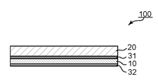
- FIG. 1 is a schematic cross-sectional view of the polarizing plate according to one embodiment of the present invention.
- the polarizing plate 100 of the illustrated example has a polarizing element 10, a protective layer (visible side protective layer) 20 bonded to the visible side of the polarizing element 10 via a first adhesive layer 31, and a first polarizing element 10.
- the adhesive layer is composed of an adhesive or an adhesive.
- the optical functional layer can be bonded via the second adhesive layer 32.
- Typical examples of the optical functional layer include another protective layer (inner protective layer) and a retardation layer.
- the inner protective layer may preferably be omitted.
- the optical functional layer is a retardation layer
- a polarizing plate with a retardation layer is configured.
- the polarizing plate with a retardation layer will be described in detail in Section B described later.
- the second adhesive layer 32 is composed of the pressure-sensitive adhesive, the polarizing plate 100 can be attached to the image display cell via the second adhesive layer 32.
- the iodine adsorption amount A1 per unit area of the first adhesive layer 31 and the iodine adsorption amount A2 per unit area of the second adhesive layer 32 satisfy the following formula (1). : (A 1 + A 2 ) ⁇ 0.300 (mg / cm 2 ) ... (1).
- (A 1 + A 2 ) is preferably 0.200 mg / cm 2 or less, more preferably 0.100 mg / cm 2 or less, still more preferably 0.080 mg / cm 2 or less, and particularly preferably 0. .060 mg / cm 2 or less.
- (A 1 + A 2 ) can be, for example, 0.020 mg / cm 2 or more.
- both A 1 and A 2 are 0.200 mg / cm 2 or less.
- (A 1 + A 2 ) is less than 0.300 mg / cm 2 and both A 1 and A 2 are 0.200 mg / cm 2 or less, the iodine in the substituent is in a high temperature and high humidity environment. It is possible to further suppress the migration to the adhesive layer in. More specifically, even if (A 1 + A 2 ) is less than 0.300 mg / cm 2 , if either A 1 or A 2 is extremely large, iodine in the substituent is in a high temperature and high humidity environment.
- one of A 1 or A 2 is preferably 0.195 mg / cm 2 or less, more preferably 0.190 mg / cm 2 or less, still more preferably 0.180 mg / cm 2 .
- the other is preferably 0.035 mg / cm 2 or less, more preferably 0.030 mg / cm 2 or less, still more preferably 0.025 mg / cm 2 or less.
- one of A 1 or A 2 can be, for example, 0.150 mg / cm 2 or more; the other can be, for example, 0.015 mg / cm 2 or more.
- a thick adhesive can be used for one of the adhesive layers.
- both A 1 and A 2 are preferably 0.045 mg / cm 2 or less, more preferably 0.040 mg / cm 2 or less, still more preferably 0.035 mg / cm 2 . It is less than or equal to, and particularly preferably 0.030 mg / cm 2 or less.
- both A 1 and A 2 can be, for example, 0.010 mg / cm 2 or more. With such a configuration, it is possible to more remarkably suppress a decrease in the degree of polarization in a high temperature and high humidity environment. Further, such a configuration can contribute to further thinning of the polarizing plate.
- the first adhesive layer 31 and the second adhesive layer 32 can each be composed of any suitable adhesive or pressure-sensitive adhesive as long as (A 1 + A 2 ) is less than 0.300 mg / cm 2 .
- the first adhesive layer 31 and the second adhesive layer 32 may both be composed of an adhesive, one may be composed of an adhesive, and the other may be composed of an adhesive. May be composed of an adhesive.
- the first adhesive layer may be composed of an adhesive and the second adhesive layer may be composed of an adhesive.
- both the first adhesive layer and the second adhesive layer may be composed of an adhesive.
- the adhesive layer is composed of an adhesive
- its thickness is preferably 2 ⁇ m or less, more preferably 1 ⁇ m or less, still more preferably 0.5 ⁇ m or less, and particularly preferably 0.3 ⁇ m or less.
- the thickness can be, for example, 0.05 ⁇ m or more.
- the thickness thereof is preferably 2 ⁇ m to 40 ⁇ m, more preferably 3 ⁇ m to 35 ⁇ m, and further preferably 4 ⁇ m to 32 ⁇ m.
- the polarizing element the protective layer, and the first adhesive layer and the second adhesive layer will be specifically described.
- any suitable polarizing element may be adopted.
- the resin film forming the polarizing element may be a single-layer resin film or a laminated body having two or more layers.
- the polarizing element composed of a single-layer resin film include a hydrophilic polymer film such as a polyvinyl alcohol (PVA) -based film, a partially formalized PVA-based film, and an ethylene / vinyl acetate copolymer-based partially saponified film.
- a hydrophilic polymer film such as a polyvinyl alcohol (PVA) -based film, a partially formalized PVA-based film, and an ethylene / vinyl acetate copolymer-based partially saponified film.
- PVA polyvinyl alcohol
- a partially formalized PVA-based film ethylene / vinyl acetate copolymer-based partially saponified film
- examples thereof include those which have been dyed and stretched with a bicolor substance such as iodine and a bicolor dye, and polyene-based oriented films such as a dehydrated product of PVA and a dehydrogenated product of polyvinyl chloride.
- the dyeing with iodine is performed, for example, by immersing a PVA-based film in an aqueous iodine solution.
- the draw ratio of the uniaxial stretching is preferably 3 to 7 times.
- the stretching may be performed after the dyeing treatment or may be performed while dyeing. Further, it may be dyed after being stretched.
- the PVA-based film is subjected to a swelling treatment, a crosslinking treatment, a cleaning treatment, a drying treatment and the like. For example, by immersing the PVA-based film in water and washing it with water before dyeing, it is possible not only to clean the dirt and blocking inhibitor on the surface of the PVA-based film, but also to swell the PVA-based film to prevent uneven dyeing. Can be prevented.
- the polarizing element obtained by using the laminate include a laminate of a resin base material and a PVA-based resin layer (PVA-based resin film) laminated on the resin base material, or a resin base material and the resin.
- Examples thereof include a polarizing element obtained by using a laminate with a PVA-based resin layer coated and formed on a base material.
- the polarizing element obtained by using the laminate of the resin base material and the PVA-based resin layer coated and formed on the resin base material is, for example, a resin base material obtained by applying a PVA-based resin solution to the resin base material and drying it.
- stretching typically includes immersing the laminate in an aqueous boric acid solution for stretching. Further, stretching may further comprise, if necessary, stretching the laminate in the air at a high temperature (eg, 95 ° C. or higher) prior to stretching in boric acid aqueous solution.
- a high temperature eg, 95 ° C. or higher
- the obtained resin base material / polarizing element laminate may be used as it is (that is, the resin base material may be used as a protective layer for the polarizing element), and the resin base material is peeled off from the resin base material / polarizing element laminate. Then, an arbitrary appropriate protective layer according to the purpose may be laminated on the peeled surface and used. Details of the method for producing such a polarizing element are described in, for example, Japanese Patent Application Laid-Open No. 2012-73580 and Japanese Patent No. 6470455. The entire description of these publications is incorporated herein by reference.
- the thickness of the splitter is preferably 15 ⁇ m or less, more preferably 12 ⁇ m or less, still more preferably 10 ⁇ m or less, and particularly preferably 8 ⁇ m or less.
- the thickness of the polarizing element may be, for example, 1 ⁇ m or more, for example, 2 ⁇ m or more, and may be, for example, 3 ⁇ m or more.
- the splitter preferably exhibits absorption dichroism at any wavelength of 380 nm to 780 nm.
- the simple substance transmittance of the polarizing element is preferably 40.0% to 45.0%, more preferably 41.0% to 44.0%, still more preferably 42.0% to 44.0%. be.
- the degree of polarization of the polarizing element is preferably 97.0% or more, more preferably 99.0% or more, and further preferably 99.9% or more.
- the visible side protective layer 20 and the inner protective layer are each formed of any suitable film that can be used as a protective layer for the stator.
- suitable film such as triacetyl cellulose (TAC), polyester-based, polyvinyl alcohol-based, polycarbonate-based, polyamide-based, polyimide-based, polyethersulfone-based, and polysulfone-based.
- TAC triacetyl cellulose
- thermosetting resins such as (meth) acrylic, urethane, (meth) acrylic urethane, epoxy, and silicone, or ultraviolet curable resins can also be mentioned.
- glassy polymers such as siloxane-based polymers can also be mentioned.
- the polymer film described in JP-A-2001-343529 (WO01 / 37007) can also be used.
- a resin composition containing a thermoplastic resin having a substituted or unsubstituted imide group in the side chain and a thermoplastic resin having a substituted or unsubstituted phenyl group and a nitrile group in the side chain.
- the polymer film can be, for example, an extruded product of the above resin composition.
- the visible side protective layer 20 may be subjected to surface treatment such as hard coat treatment, antireflection treatment, sticking prevention treatment, and antiglare treatment, if necessary. Further / or, if necessary, the visual-viewing side protective layer 20 is provided with a process for improving visibility when visually recognizing through polarized sunglasses (typically, a (elliptical) circular polarization function is imparted, super. (To give a high phase difference) may be applied. By performing such processing, excellent visibility can be realized even when the display screen is visually recognized through a polarizing lens such as polarized sunglasses. Therefore, the polarizing plate and the polarizing plate with a retardation layer can be suitably applied to an image display device that can be used outdoors.
- surface treatment such as hard coat treatment, antireflection treatment, sticking prevention treatment, and antiglare treatment, if necessary.
- the visual-viewing side protective layer 20 is provided with a process for improving visibility when visually recognizing through polarized sunglasses (typically, a (elliptical) circular polar
- the thickness of the visible side protective layer 20 is preferably 10 ⁇ m to 50 ⁇ m, more preferably 15 ⁇ m to 35 ⁇ m. When the surface treatment is applied, the thickness of the visible side protective layer 20 is the thickness including the thickness of the surface treatment layer.
- the inner protective layer is preferably optically isotropic in one embodiment.
- optically isotropic means that the in-plane retardation Re (550) is 0 nm to 10 nm and the thickness direction retardation Rth (550) is -10 nm to +10 nm. say.
- the thickness of the other protective layer is preferably 5 ⁇ m to 80 ⁇ m, more preferably 10 ⁇ m to 40 ⁇ m, and even more preferably 10 ⁇ m to 30 ⁇ m.
- the inner protective layer may preferably be omitted.
- the first adhesive layer and the second adhesive layer are arbitrary as long as (A 1 + A 2 ) is less than 0.300 mg / cm 2 . It may be composed of a suitable adhesive or adhesive. Again, as described above, the first adhesive layer and the second adhesive layer may both be composed of an adhesive, one may be composed of an adhesive and the other may be composed of an adhesive, and both may be composed of an adhesive. It may be composed of an adhesive. In one embodiment, the first adhesive layer may be composed of an adhesive and the second adhesive layer may be composed of an adhesive. In another embodiment, both the first adhesive layer and the second adhesive layer may be composed of an adhesive. In this section, the first adhesive layer and the second adhesive layer may be collectively referred to as an adhesive layer.
- a typical example of the adhesive is a water-based adhesive.
- a water-based adhesive By using a water-based adhesive, an extremely thin adhesive layer (for example, 0.3 ⁇ m or less) can be formed.
- the water-based adhesive preferably contains a PVA-based resin.
- the average degree of polymerization of the PVA-based resin contained in the water-based adhesive is preferably about 100 to 5000, more preferably 1000 to 4000, from the viewpoint of adhesiveness.
- the average saponification degree is preferably about 85 mol% to 100 mol%, more preferably 90 mol% to 100 mol% from the viewpoint of adhesiveness.
- the PVA-based resin preferably contains an acetoacetyl group. This is because the adhesion between the polarizing element and the protective layer is excellent, and the durability can be excellent.
- the acetoacetyl group-containing PVA-based resin can be obtained, for example, by reacting the PVA-based resin with diketene by an arbitrary method.
- the degree of acetoacetyl group modification of the acetoacetyl group-containing PVA resin is typically 0.1 mol% or more, preferably about 0.1 mol% to 40 mol%, and more preferably 1 mol% to 20 mol. %, Especially preferably 2 mol% to 7 mol%.
- the degree of acetoacetyl group modification is a value measured by NMR.
- the form of the water-based adhesive (before curing) is preferably a liquid (typically an aqueous solution).
- the resin concentration in the liquid is preferably 0.1% by weight to 15% by weight, more preferably 0.5% by weight to 10% by weight.
- the viscosity of the liquid is preferably 1 to 50 mPa ⁇ s.
- the pH of the liquid is preferably 2 to 6, more preferably 2.5 to 5, still more preferably 3 to 5, and particularly preferably 3.5 to 4.5.
- the water-based adhesive may preferably contain a metal compound colloid.
- the metal compound colloid is one in which the metal compound fine particles are dispersed in the dispersion medium, and is electrostatically stabilized due to the mutual repulsion of the same kind of charges of the fine particles, and can have permanent stability. ..
- By including such a metal compound colloid it is possible to form an adhesive layer in which the amount of iodine adsorbed per unit area is very small.
- a knick defect a defect that causes light leakage
- the present inventors have achieved a remarkable effect by using an aqueous adhesive containing a metal compound colloid.
- a remarkable effect could be obtained due to the very small amount of iodine adsorbed per unit area of the adhesive layer.
- Such a very small amount of iodine adsorbed per unit area is a synergistic effect of the effect of forming a very thin adhesive layer, the effect of the binder resin being a PVA-based resin, and the effect of the metal compound colloid. It is presumed that this is due to.
- the average particle size of the fine particles forming the metal compound colloid is set to an arbitrary appropriate value as long as it does not adversely affect the optical characteristics such as transparency and polarization characteristics. It is preferably 1 nm to 100 nm, more preferably 1 nm to 50 nm. This is because the fine particles can be uniformly dispersed in the adhesive layer.
- metal compound any suitable compound is used.
- metal oxides such as alumina, silica, zirconia and titania
- metal salts such as aluminum silicate, calcium carbonate, magnesium silicate, zinc carbonate, barium carbonate and calcium phosphate
- minerals such as celite, talc, clay and kaolin.
- a positively charged metal compound colloid is preferably used.
- the metal compound include alumina, titania and the like, and alumina is particularly preferable.
- the amount of the metal compound colloid (solid content) blended is preferably 200 parts by weight or less, more preferably 10 parts by weight to 200 parts by weight, and further preferably 20 parts by weight to 175 parts by weight with respect to 100 parts by weight of the PVA-based resin. Parts, particularly preferably 30 parts by weight to 150 parts by weight.
- the water-based adhesive may further contain additives.
- the additive include a cross-linking agent (for example, a compound having at least two functional groups reactive with a PVA-based resin); a coupling agent such as a silane coupling agent and a titanium coupling agent; various adhesives.
- the adhesive include an acrylic adhesive, a rubber adhesive, a silicone adhesive, a polyester adhesive, a urethane adhesive, an epoxy adhesive, and a polyether adhesive.
- an acrylic adhesive By adjusting the type, number, combination and blending ratio of the monomers forming the base resin of the pressure-sensitive adhesive, the blending amount of the cross-linking agent, the reaction temperature, the reaction time, etc., the pressure-sensitive adhesive having desired characteristics according to the purpose. Can be prepared.
- the base resin of the pressure-sensitive adhesive may be used alone or in combination of two or more.
- An acrylic pressure-sensitive adhesive (acrylic pressure-sensitive adhesive composition) is preferable from the viewpoint of transparency, processability, durability and the like.
- the acrylic pressure-sensitive adhesive composition typically contains a (meth) acrylic polymer as a main component.
- the (meth) acrylic polymer can be contained in the pressure-sensitive adhesive composition in a proportion of, for example, 50% by weight or more, preferably 70% by weight or more, and more preferably 90% by weight or more in the solid content of the pressure-sensitive adhesive composition.
- the (meth) acrylic polymer contains an alkyl (meth) acrylate as a main component as a monomer unit.
- (meth) acrylate means acrylate and / or methacrylate.
- the alkyl (meth) acrylate may be contained in a proportion of preferably 80% by weight or more, more preferably 90% by weight or more, in the monomer component forming the (meth) acrylic polymer.
- alkyl group of the alkyl (meth) acrylate examples include a linear or branched alkyl group having 1 to 18 carbon atoms. The average number of carbon atoms of the alkyl group is preferably 3 to 9, and more preferably 3 to 6.
- the preferred alkyl (meth) acrylate is butyl acrylate.
- the monomer (copolymerization monomer) constituting the (meth) acrylic polymer in addition to the alkyl (meth) acrylate, a carboxyl group-containing monomer, a hydroxyl group-containing monomer, an amide group-containing monomer, an aromatic ring-containing (meth) acrylate, and a complex Examples include ring-containing vinyl-based monomers.
- the copolymerized monomer examples include acrylic acid, 2-hydroxyethyl acrylate, 4-hydroxybutyl acrylate, acryloyl morpholine, phenoxyethyl acrylate, and N-vinyl-2-pyrrolidone.
- Acrylic acid, 4-hydroxybutyl acrylate, and acryloyl morpholine are preferable.
- an adhesive layer having a small iodine adsorption amount per unit area can be formed.
- the acrylic pressure-sensitive adhesive composition may preferably contain a silane coupling agent and / or a cross-linking agent.
- the silane coupling agent include epoxy group-containing silane coupling agents.
- cross-linking agent examples include isocyanate-based cross-linking agents and peroxide-based cross-linking agents.
- acrylic pressure-sensitive adhesive composition may contain an antioxidant and / or a conductive agent. Details of the pressure-sensitive adhesive are described in, for example, JP-A-2006-183022, JP-A-2015-199942, JP-A-2018-053114, JP-A-2016-190996, and International Publication No. 2018/008712. The description of these publications is incorporated herein by reference.
- the adhesive has a storage elastic modulus at 25 ° C., preferably 1.0 ⁇ 10 4 Pa to 1.0 ⁇ 10 6 Pa, and more preferably 1.0 ⁇ 10 4 Pa to 1.0 ⁇ 10 5 Pa. Is.
- the storage elastic modulus of the pressure-sensitive adhesive is within such a range, the internal stress due to the dimensional change of the polarizing element can be relaxed at the time of heating and / or at the time of bending or bonding to a curved surface.
- the pressure-sensitive adhesive may have a creep amount ⁇ Cr at 70 ° C. of, for example, 65 ⁇ m or less, 50 ⁇ m or less, 45 ⁇ m or less, 40 ⁇ m or less, 35 ⁇ m or less, 30 ⁇ m or less, 25 ⁇ m or less, 20 ⁇ m or less, and further 15 ⁇ m or less.
- the lower limit of the creep amount ⁇ Cr is, for example, 0.5 ⁇ m. If the creep amount is in such a range, the internal stress due to the dimensional change of the stator can be relaxed at the time of heating and / or at the time of bending or bonding to a curved surface, as in the case of the storage elastic modulus. can.
- the polarizing plate according to the embodiment of the present invention has a retardation layer in which the retardation layers are bonded via a second adhesive layer 32.
- a polarizing plate may be configured. Therefore, a polarizing plate with a retardation layer can also be included in the embodiment of the present invention.
- the polarizing plate with a retardation layer according to the embodiment of the present invention can maintain optical characteristics even in a high temperature and high humidity environment, and can realize an image display device with small display unevenness.
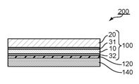
- FIG. 2 is a schematic cross-sectional view of a polarizing plate with a retardation layer according to one embodiment of the present invention.
- the polarizing plate 200 with a retardation layer of the illustrated example has a polarizing plate 100 and a retardation layer 120 bonded to the polarizing plate 100 via a second adhesive layer 32.
- the retardation layer 120 typically has a circular polarization function or an elliptically polarizing function.
- an adhesive layer 140 is provided as an outermost layer on the side opposite to the viewing side on the side opposite to the polarizing plate 100 of the retardation layer 120, and the polarizing plate with a retardation layer is used as an image display cell. It is said that it can be pasted.
- the pressure-sensitive adhesive layer 140 may be composed of any suitable pressure-sensitive adhesive. Practically, a separator (not shown) is temporarily attached to the surface of the pressure-sensitive adhesive layer 140 so as to be peelable. By temporarily attaching the separator, the pressure-sensitive adhesive layer can be protected and a roll of the polarizing plate with a retardation layer can be formed.
- the retardation layer is typically an orientation-solidified layer of a liquid crystal compound.
- a liquid crystal compound By using a liquid crystal compound, the difference between nx and ny of the obtained retardation layer can be significantly increased as compared with the non-liquid crystal material, so that the thickness of the retardation layer for obtaining a desired in-plane retardation can be obtained. Can be made much smaller. As a result, it is possible to realize a remarkable reduction in thickness of the polarizing plate with a retardation layer.
- the term "aligned solidified layer” refers to a layer in which a liquid crystal compound is oriented in a predetermined direction within the layer and the oriented state is fixed.
- the "oriented solidified layer” is a concept including an oriented cured layer obtained by curing a liquid crystal monomer as described later.
- the rod-shaped liquid crystal compounds are typically oriented in a state of being aligned in the slow axis direction of the retardation layer (homogeneous orientation).
- the retardation layer is a single layer 120.
- the retardation layer typically exhibits reverse dispersion wavelength characteristics and can function as a ⁇ / 4 plate.
- the Re (550) of the retardation layer is preferably 100 nm to 190 nm, and the Re (450) / Re (550) is preferably 0.8 to 0.95, which is a delay of the retardation layer.
- the angle formed by the phase axis and the absorption axis of the substituent is preferably 40 ° to 50 °.
- the retardation layer has a first retardation layer 121 and a second retardation layer 122.
- first retardation layer 121 or the second retardation layer 122 can function as a ⁇ / 2 plate and the other can function as a ⁇ / 4 plate.
- the Re (550) of the first retardation layer 121 can be used.
- the total thickness of the polarizing plate with a retardation layer is preferably 80 ⁇ m or less, more preferably 70 ⁇ m or less, still more preferably 65 ⁇ m or less, and particularly preferably. It is 60 ⁇ m or less.
- the lower limit of the total thickness can be, for example, 42 ⁇ m. According to the embodiment of the present invention, the decrease in the degree of polarization of the polarizing element is suppressed in such an extremely thin and high temperature and high humidity environment, and as a result, the overall optical characteristics are maintained in the high temperature and high humidity environment. It is possible to realize a polarizing plate with a possible retardation layer.
- a polarizing plate with a retardation layer having such a total thickness can have extremely excellent flexibility and bendability.
- the polarizing plate with a retardation layer can be particularly preferably applied to a curved image display device and / or a bendable or bendable image display device.
- the polarizing plate with a retardation layer may further include other optical functional layers.
- the type, characteristics, number, combination, arrangement position, and the like of the optical functional layers that can be provided on the polarizing plate with a retardation layer can be appropriately set according to the purpose.
- the polarizing plate with a retardation layer may further have a conductive layer or an isotropic substrate with a conductive layer (neither is shown).
- the conductive layer or the isotropic base material with the conductive layer is typically provided on the outside of the retardation layer 120 (on the opposite side of the polarizing plate 100).
- the conductive layer or the isotropic base material with the conductive layer is typically any layer provided as needed, and may be omitted.
- the polarizing plate with a retardation layer is a so-called inner in which a touch sensor is incorporated between an image display cell (for example, an organic EL cell) and the polarizing plate. It can be applied to a touch panel type input display device.
- the polarizing plate with a retardation layer may further include another retardation layer.
- the optical characteristics for example, refractive index characteristics, in-plane retardation, Nz coefficient, photoelastic coefficient
- thickness, arrangement position, and the like of the other retardation layer can be appropriately set according to the purpose.
- the polarizing plate with a retardation layer may be single-wafer-shaped or long-shaped.
- the term "long” means an elongated shape having a length sufficiently long with respect to the width, and for example, an elongated shape having a length of 10 times or more, preferably 20 times or more with respect to the width. include.
- the long polarizing plate with a retardation layer can be wound in a roll shape.
- the retardation layer will be described below.
- the first retardation layer and the second retardation layer are collectively described as a retardation layer, and the first position is described.
- the "first” and “second” are referred to only when it is necessary to distinguish between the retardation layer and the second retardation layer.
- the retardation layer is an oriented solidified layer of a liquid crystal compound (hereinafter referred to as a liquid crystal oriented solidified layer).
- the liquid crystal compound include a liquid crystal compound (nematic liquid crystal) in which the liquid crystal phase is a nematic phase.
- a liquid crystal compound for example, a liquid crystal polymer or a liquid crystal monomer can be used.
- the liquid crystal expression mechanism of the liquid crystal compound may be either lyotropic or thermotropic.
- the liquid crystal polymer and the liquid crystal monomer may be used alone or in combination.
- the liquid crystal monomer is preferably a polymerizable monomer and a crosslinkable monomer. This is because the orientation state of the liquid crystal monomer can be fixed by polymerizing or cross-linking (that is, curing) the liquid crystal monomer. After the liquid crystal monomers are oriented, for example, if the liquid crystal monomers are polymerized or crosslinked with each other, the oriented state can be fixed.
- the polymer is formed by polymerization, and the three-dimensional network structure is formed by crosslinking, but these are non-liquid crystal.
- the formed retardation layer does not undergo a transition to a liquid crystal phase, a glass phase, or a crystal phase due to a temperature change peculiar to a liquid crystal compound, for example.
- the retardation layer becomes an extremely stable retardation layer that is not affected by temperature changes.
- the temperature range in which the liquid crystal monomer exhibits liquid crystal properties differs depending on the type. Specifically, the temperature range is preferably 40 ° C. to 120 ° C., more preferably 50 ° C. to 100 ° C., and most preferably 60 ° C. to 90 ° C.
- any suitable liquid crystal monomer can be adopted as the liquid crystal monomer.
- the polymerizable mesogen compounds described in Special Tables 2002-533742 WO00 / 37585
- EP358208 US5211877
- EP66137 US43884553
- WO93 / 22397 EP0261712, DE19504224, DE4408171, and GB2280445
- Specific examples of such a polymerizable mesogen compound include, for example, BASF's trade name LC242, Merck's trade name E7, and Wacker-Chem's trade name LC-Silicon-CC3767.
- the liquid crystal monomer for example, a nematic liquid crystal monomer is preferable.
- the surface of a predetermined base material is subjected to an orientation treatment, and a coating liquid containing a liquid crystal compound is applied to the surface to orient the liquid crystal compound in a direction corresponding to the alignment treatment. It can be formed by fixing the state.
- the substrate is any suitable resin film and the liquid crystal oriented solidified layer (phase difference layer 120 or first retardation layer 121) formed on the substrate is a second. It can be transferred to the surface of the polarizing plate 100 via the adhesive layer 32. If the retardation layer has a first retardation layer 121 and a second retardation layer 122, the second retardation layer 122 formed on the substrate is a second via any suitable adhesive. It can be transferred to the surface of the retardation layer 121 of 1.
- any appropriate orientation treatment can be adopted.
- Specific examples thereof include mechanical orientation treatment, physical orientation treatment, and chemical orientation treatment.
- Specific examples of the mechanical orientation treatment include a rubbing treatment and a stretching treatment.
- Specific examples of the physical orientation treatment include magnetic field orientation treatment and electric field orientation treatment.
- Specific examples of the chemical alignment treatment include an orthorhombic vapor deposition method and a photoalignment treatment.
- As the treatment conditions for various orientation treatments any appropriate conditions may be adopted depending on the purpose.
- the orientation of the liquid crystal compound is performed by treating at a temperature indicating the liquid crystal phase according to the type of the liquid crystal compound. By performing such temperature treatment, the liquid crystal compound takes a liquid crystal state, and the liquid crystal compound is oriented according to the orientation treatment direction of the surface of the substrate.
- the alignment state is fixed by cooling the liquid crystal compound oriented as described above.
- the orientation state is fixed by subjecting the liquid crystal compound oriented as described above to a polymerization treatment or a crosslinking treatment.
- liquid crystal compound and details of the method for forming the oriented solidified layer are described in Japanese Patent Application Laid-Open No. 2006-163343. The description of this publication is incorporated herein by reference.
- the retardation layer preferably has an Nz coefficient of 0.9 to 1.5, and more preferably 0.9 to 1.3. By satisfying such a relationship, a very excellent reflected hue can be achieved when the obtained polarizing plate with a retardation layer is used in an image display device.
- the in-plane retardation Re (550) of the retardation layer is preferably 100 nm to 190 nm, more preferably 110 nm to 170 nm, and further preferably 130 nm to 160 nm as described above.
- Re (450) / Re (550) is preferably 0.8 to 0.95 as described above.
- the angle formed by the slow axis of the retardation layer and the absorption axis of the polarizing element is preferably 40 ° to 50 °, more preferably 42 ° to 48 °, and further preferably about 45 ° as described above. °.
- the retardation layer has a first retardation layer 121 and a second retardation layer 122
- first retardation layer 121 or the second retardation layer 122 functions as a ⁇ / 2 plate.
- the other can function as a ⁇ / 4 plate.
- first retardation layer 121 can function as a ⁇ / 2 plate and the second retardation layer 122 can function as a ⁇ / 4 plate will be described, but these may be reversed. ..
- the thickness of the first retardation layer 121 can be adjusted to obtain the desired in-plane retardation of the ⁇ / 2 plate, for example 1.5 ⁇ m to 2.5 ⁇ m.
- the thickness of the second retardation layer 122 can be adjusted to obtain the desired in-plane retardation of the ⁇ / 4 plate, for example 0.5 ⁇ m to 1.5 ⁇ m.
- the in-plane retardation Re (550) of the first retardation layer is preferably 200 nm to 300 nm, more preferably 230 nm to 290 nm, and further preferably 250 nm to 280 nm as described above.
- the in-plane retardation Re (550) of the second retardation layer is preferably 100 nm to 190 nm, more preferably 110 nm to 170 nm, and further preferably 130 nm to 160 nm as described above.
- the angle formed by the slow axis of the first retardation layer 121 and the absorption axis of the polarizing element 10 is preferably 10 ° to 20 °, more preferably 12 ° to 18 °, and further preferably 12 ° to 18 °, as described above. Is about 15 °.
- the angle formed by the slow axis of the second retardation layer 122 and the absorption axis of the polarizing element 10 is preferably 70 ° to 80 °, more preferably 72 ° to 78 °, and even more preferably, as described above. Is about 75 °. With such a configuration, it is possible to obtain characteristics close to the ideal reverse wavelength dispersion characteristic, and as a result, it is possible to realize extremely excellent antireflection characteristics.
- the first retardation layer and the second retardation layer may each exhibit a reverse dispersion wavelength characteristic in which the retardation value increases according to the wavelength of the measurement light, and the retardation value depends on the wavelength of the measurement light. It may show a small positive wavelength dispersion characteristic, or may show a flat wavelength dispersion characteristic in which the phase difference value hardly changes depending on the wavelength of the measured light.
- Image display device The polarizing plate according to the above item A and the polarizing plate with a retardation layer according to the above item B can be applied to an image display device. Therefore, an image display device including a polarizing plate or a polarizing plate with a retardation layer is also included in the embodiment of the present invention.
- the image display device typically includes an image display cell and a polarizing plate or a polarizing plate with a retardation layer attached to the image display cell via an adhesive layer.
- the polarizing plate or the polarizing plate with a retardation layer can be typically arranged on the visual side of the image display cell.
- the image display device include a liquid crystal display device and an electroluminescence (EL) display device (for example, an organic EL display device and an inorganic EL display device).
- the image display device is an organic EL display device.
- the image display device has a curved shape (substantially a curved display screen) and / or is bendable or bendable. In such an image display device, the effect of the polarizing plate with a retardation layer according to the embodiment of the present invention becomes remarkable.
- Thickness The thickness of 10 ⁇ m or less was measured using an interference film thickness meter (manufactured by Otsuka Electronics Co., Ltd., product name “MCPD-3000”). Thicknesses exceeding 10 ⁇ m were measured using a digital micrometer (manufactured by Anritsu, product name “KC-351C”).
- Iodine adsorption amount 10 g of 0.127% iodine aqueous solution was placed in a glass bottle having a capacity of 500 mL.
- the adhesive or adhesive used in Examples and Comparative Examples was cut out to a predetermined size and used as a measurement material. This measurement material was attached to the inside of the lid of the glass bottle, and the glass bottle was sealed with the lid.
- the measurement data was hung inside the sealed glass bottle.
- the distance between the lower end of the measurement data and the liquid level of the iodine aqueous solution was about 40 mm.
- the glass bottle was heated at 65 ° C. for 6 hours. After heating, the measurement sample was taken out, and the iodine detection intensity (kcps) was measured with a scanning fluorescent X-ray analyzer (“ZSX Primus IV” manufactured by RIGAKU).
- Mw weight average molecular weight
- UV Curable Adhesive A commercially available UV curable adhesive was used.
- Example 1 Fabrication of Polarizer
- a thermoplastic resin base material an amorphous isophthal copolymer polyethylene terephthalate film (thickness: 100 ⁇ m) having a long shape and a Tg of about 75 ° C. was used, and one side of the resin base material was treated with corona. Was given. 100 parts by weight of PVA-based resin in which polyvinyl alcohol (polymerization degree 4200, saponification degree 99.2 mol%) and acetacetyl-modified PVA (manufactured by Nippon Synthetic Chemical Industry Co., Ltd., trade name "Gosefimer”) are mixed at a ratio of 9: 1.
- a PVA aqueous solution (coating solution) was prepared by dissolving 13 parts by weight of potassium iodide in water.
- the PVA aqueous solution was applied to the corona-treated surface of the resin base material and dried at 60 ° C. to form a PVA-based resin layer having a thickness of 13 ⁇ m, and a laminate was prepared.
- the obtained laminate was uniaxially stretched 2.4 times in the vertical direction (longitudinal direction) in an oven at 130 ° C. (aerial auxiliary stretching treatment). Next, the laminate was immersed in an insolubilizing bath at a liquid temperature of 40 ° C.
- boric acid aqueous solution obtained by blending 3 parts by weight of potassium iodide and 5 parts by weight of boric acid with respect to 100 parts by weight of water
- a boric acid aqueous solution obtained by blending 3 parts by weight of potassium iodide and 5 parts by weight of boric acid with respect to 100 parts by weight of water
- a boric acid aqueous solution boric acid concentration 4% by weight, potassium iodide concentration 5% by weight
- Uniaxial stretching was performed so that the stretching ratio was 5.5 times (underwater stretching treatment).
- the laminate was immersed in a washing bath having a liquid temperature of 20 ° C.
- HC-TAC film is applied to the surface of the polarizing element of the resin substrate / polarizing element laminate obtained above via the adhesive A (first adhesive layer) obtained in Production Example 1. I pasted them together. Specifically, the adhesive A was coated so that the thickness after drying was 0.1 ⁇ m, and the adhesive A was bonded using a roll machine, and then the adhesive A was dried.
- the HC-TAC film is a film in which a hard coat (HC) layer (thickness 7 ⁇ m) is formed on a triacetyl cellulose (TAC) film (thickness 25 ⁇ m), and the TAC film is attached so as to be on the splitter side. I matched it.
- the resin base material is peeled off, the pressure-sensitive adhesive C (thickness 5 ⁇ m) obtained in Production Example 3 is placed on the peeled surface, and the visible side protective layer (HC-TAC film) / first adhesive layer (adhesive) is placed.
- Phase Difference Layer 55 parts of the compound represented by the formula (II), 25 parts of the compound represented by the formula (III), and 20 parts of the compound represented by the formula (IV) are added to 400 parts of cyclopentanone (CPN). After addition, heat to 60 ° C., stir to dissolve, and after confirmation of dissolution, return to room temperature, Irga Cure 907 (manufactured by BASF Japan Co., Ltd.), 3 parts, Megafuck F-554 (manufactured by DIC Corporation). 0.2 part and 0.1 part of p-methoxyphenol (MEHQ) were added, and the mixture was further stirred to obtain a solution. The solution was clear and uniform.
- CPN cyclopentanone
- the obtained solution was filtered through a 0.20 ⁇ m membrane filter to obtain a polymerizable composition.
- a polyimide solution for an alignment film was applied to a glass substrate having a thickness of 0.7 mm by a spin coating method, dried at 100 ° C. for 10 minutes, and then fired at 200 ° C. for 60 minutes to obtain a coating film. ..
- the obtained coating film was subjected to a rubbing treatment to form an alignment film. The rubbing treatment was performed using a commercially available rubbing device.
- the polymerizable composition obtained above was applied to a substrate (substantially an alignment film) by a spin coating method, and dried at 100 ° C. for 2 minutes.
- the obtained coating film was cooled to room temperature and then irradiated with ultraviolet rays at an intensity of 30 mW / cm 2 for 30 seconds using a high-pressure mercury lamp to obtain a liquid crystal oriented solidified layer.
- the thickness of the liquid crystal oriented solidified layer was 2.8 ⁇ m, and the in-plane retardation Re (550) was 130 nm.
- the Re (450) / Re (550) of the liquid crystal oriented solidified layer was 0.851, showing the reverse dispersion wavelength characteristic. This liquid crystal oriented solidified layer was used as a retardation layer.
- the liquid crystal is formed by applying the coating liquid to a base film (norbornene-based resin film: manufactured by Nippon Zeon Corporation, trade name "Zeonex”) with a bar coater, and then heating and drying at 80 ° C. for 4 minutes. Oriented.
- a liquid crystal oriented solidified layer positive C plate, thickness 3 ⁇ m
- Re (590) of this layer was 0 nm
- polarizing plate with retardation layer 2 Fabrication of polarizing plate with retardation layer 2.
- the liquid crystal oriented solidified layer obtained in 3-1 was transferred to the surface of the second adhesive layer of the polarizing plate obtained in 1 above, and further, the surface of the liquid crystal oriented solidified layer was transferred to the surface of the liquid crystal oriented solidified layer via an ultraviolet curable adhesive to the above 3-2.
- the positive C plate obtained in 1) was transferred to the visible side protective layer (HC-TAC film) / first adhesive layer (adhesive A) / polarizing element / second adhesive layer (adhesive C) / retardation layer.
- a polarizing plate with a retardation layer having the structure of / adhesive / positive C plate was obtained.
- the obtained polarizing plate with a retardation layer was subjected to the evaluation of (3) above. The results are shown in Table 1.
- Example 2 A polarizing plate with a retardation layer was obtained in the same manner as in Example 1 except that the thickness of the second adhesive layer (adhesive C) was changed from 5 ⁇ m to 30 ⁇ m. The obtained polarizing plate with a retardation layer was subjected to the same evaluation as in Example 1. The results are shown in Table 1.
- Example 3 A polarizing plate with a retardation layer was obtained in the same manner as in Example 1 except that the adhesive B obtained in Production Example 2 was used instead of the adhesive A obtained in Production Example 1 as the first adhesive layer. rice field. The obtained polarizing plate with a retardation layer was subjected to the same evaluation as in Example 1. The results are shown in Table 1.
- Example 4 to 12 and Comparative Examples 1 to 6 A polarizing plate with a retardation layer was obtained by combining the visible side protective layer, the first adhesive layer and the second adhesive layer as shown in Table 1. The obtained polarizing plate with a retardation layer was subjected to the same evaluation as in Example 1. The results are shown in Table 1.
- HC-TAC is the above-mentioned HC-TAC film
- HC-COP is a film in which an HC layer (thickness 2 ⁇ m) is formed on a cycloolefin resin (COP) film (thickness 25 ⁇ m)
- acrylic is an acrylic film.
- the iodine adsorption amount A1 per unit area of the first adhesive layer and the iodine adsorption amount A2 per unit area of the second adhesive layer By setting the total to a predetermined value or less, it is possible to realize a polarizing plate having a thin shape and suppressing a decrease in the degree of polarization in a high temperature and high humidity environment and a polarizing plate with a retardation layer.
- the polarizing plate with the present invention and the polarizing plate with a retardation layer are suitably used as a circular polarizing plate for a liquid crystal display device, an organic EL display device, and an inorganic EL display device.
- Polarizer 10 Polarizer 20 Protective layer 31 First adhesive layer 32 Second adhesive layer 100 Polarizing plate 120 Phase difference layer 121 First retardation layer 122 Second phase difference layer 140 Adhesive layer 200 Polarizing plate with retardation layer
Landscapes
- Physics & Mathematics (AREA)
- General Physics & Mathematics (AREA)
- Optics & Photonics (AREA)
- Chemical & Material Sciences (AREA)
- Crystallography & Structural Chemistry (AREA)
- Nonlinear Science (AREA)
- Mathematical Physics (AREA)
- Polarising Elements (AREA)
- Liquid Crystal (AREA)
- Electroluminescent Light Sources (AREA)
Abstract
薄型で、かつ、高温高湿環境下における偏光度の低下が抑制された偏光板および位相差層付偏光板が提供される。本発明の実施形態による偏光板は、偏光子と、偏光子の視認側に第1の接着層を介して貼り合わせられた保護層と、偏光子の第1の接着層と反対側に配置された第2の接着層と、を含む。第1の接着層の単位面積あたりのヨウ素吸着量A1および第2の接着層の単位面積あたりのヨウ素吸着量A2は下記式(1)を満足する: (A1+A2)<0.300(mg/cm2) ・・・(1)。 本発明の位相差層付偏光板は、この偏光板と;偏光板に第2の接着層を介して貼り合わせられた、円偏光機能または楕円偏光機能を有する位相差層と;を有する。
Description
本発明は、偏光板、位相差層付偏光板および画像表示装置に関する。
近年、液晶表示装置およびエレクトロルミネセンス(EL)表示装置(例えば、有機EL表示装置、無機EL表示装置)に代表される画像表示装置が急速に普及している。画像表示装置には、代表的には偏光板および位相差板が用いられている。実用的には、偏光板と位相差板と粘着剤層とを一体化した位相差層付偏光板が広く用いられている(例えば、特許文献1)。最近、画像表示装置の薄型化への要望が強くなるに伴って、偏光板および位相差層付偏光板についても薄型化の要望が強まっている。しかし、薄型の偏光板においては、高温高湿環境下において偏光度の低下が大きいという問題がある。さらに、このような偏光板を用いた薄型の位相差層付偏光板においても同様の問題が生じ得る。
本発明は上記従来の課題を解決するためになされたものであり、その主たる目的は、薄型で、かつ、高温高湿環境下における偏光度の低下が抑制された偏光板および位相差層付偏光板を提供することにある。
本発明の実施形態による偏光板は、偏光子と、該偏光子の視認側に第1の接着層を介して貼り合わせられた保護層と、該偏光子の該第1の接着層と反対側に配置された第2の接着層と、を含む。該第1の接着層の単位面積あたりのヨウ素吸着量A1および該第2の接着層の単位面積あたりのヨウ素吸着量A2は下記式(1)を満足する:
(A1+A2)<0.300(mg/cm2) ・・・(1)。
1つの実施形態においては、上記A1および上記A2はいずれも0.200mg/cm2以下である。
1つの実施形態においては、上記第1の接着層および/または上記第2の接着層の厚みは0.3μm以下である。
1つの実施形態においては、上記偏光子の厚みは10μm以下である。
1つの実施形態においては、上記偏光子の単体透過率は40.0%~45.0%である。
本発明の別の局面によれば、位相差層付偏光板が提供される。この位相差層付偏光板は、上記偏光板と;該偏光板に上記第2の接着層を介して貼り合わせられた、円偏光機能または楕円偏光機能を有する位相差層と;を有する。
1つの実施形態においては、上記位相差層は液晶化合物の配向固化層である。
1つの実施形態においては、上記位相差層は単一層であり、該位相差層のRe(550)は100nm~190nmであり、Re(450)/Re(550)は0.8~0.95であり、その遅相軸と上記偏光子の吸収軸とのなす角度は40°~50°である。
1つの実施形態においては、上記位相差層は、第1の位相差層と第2の位相差層とを有し;該第1の位相差層のRe(550)は200nm~300nmであり、その遅相軸と上記偏光子の吸収軸とのなす角度が10°~20°であり;該第2の位相差層のRe(550)は100nm~190nmであり、その遅相軸と該偏光子の吸収軸とのなす角度は70°~80°である。
本発明のさらに別の局面によれば、画像表示装置が提供される。この画像表示装置は、上記偏光板または上記位相差層付偏光板を備える。
(A1+A2)<0.300(mg/cm2) ・・・(1)。
1つの実施形態においては、上記A1および上記A2はいずれも0.200mg/cm2以下である。
1つの実施形態においては、上記第1の接着層および/または上記第2の接着層の厚みは0.3μm以下である。
1つの実施形態においては、上記偏光子の厚みは10μm以下である。
1つの実施形態においては、上記偏光子の単体透過率は40.0%~45.0%である。
本発明の別の局面によれば、位相差層付偏光板が提供される。この位相差層付偏光板は、上記偏光板と;該偏光板に上記第2の接着層を介して貼り合わせられた、円偏光機能または楕円偏光機能を有する位相差層と;を有する。
1つの実施形態においては、上記位相差層は液晶化合物の配向固化層である。
1つの実施形態においては、上記位相差層は単一層であり、該位相差層のRe(550)は100nm~190nmであり、Re(450)/Re(550)は0.8~0.95であり、その遅相軸と上記偏光子の吸収軸とのなす角度は40°~50°である。
1つの実施形態においては、上記位相差層は、第1の位相差層と第2の位相差層とを有し;該第1の位相差層のRe(550)は200nm~300nmであり、その遅相軸と上記偏光子の吸収軸とのなす角度が10°~20°であり;該第2の位相差層のRe(550)は100nm~190nmであり、その遅相軸と該偏光子の吸収軸とのなす角度は70°~80°である。
本発明のさらに別の局面によれば、画像表示装置が提供される。この画像表示装置は、上記偏光板または上記位相差層付偏光板を備える。
本発明の実施形態によれば、偏光板において、偏光子に隣接する接着層の単位面積あたりのヨウ素吸着量を所定値以下とすることにより、薄型で、かつ、高温高湿環境下における偏光度の低下が抑制された偏光板を得ることができる。結果として、高温高湿環境下において光学特性を維持し得、表示ムラの小さい画像表示装置を実現し得る位相差層付偏光板を得ることができる。
以下、本発明の実施形態について説明するが、本発明はこれらの実施形態には限定されない。
(用語および記号の定義)
本明細書における用語および記号の定義は下記の通りである。
(1)屈折率(nx、ny、nz)
「nx」は面内の屈折率が最大になる方向(すなわち、遅相軸方向)の屈折率であり、「ny」は面内で遅相軸と直交する方向(すなわち、進相軸方向)の屈折率であり、「nz」は厚み方向の屈折率である。
(2)面内位相差(Re)
「Re(λ)」は、23℃における波長λnmの光で測定した面内位相差である。例えば、「Re(550)」は、23℃における波長550nmの光で測定した面内位相差である。Re(λ)は、層(フィルム)の厚みをd(nm)としたとき、式:Re(λ)=(nx-ny)×dによって求められる。
(3)厚み方向の位相差(Rth)
「Rth(λ)」は、23℃における波長λnmの光で測定した厚み方向の位相差である。例えば、「Rth(550)」は、23℃における波長550nmの光で測定した厚み方向の位相差である。Rth(λ)は、層(フィルム)の厚みをd(nm)としたとき、式:Rth(λ)=(nx-nz)×dによって求められる。
(4)Nz係数
Nz係数は、Nz=Rth/Reによって求められる。
(5)角度
本明細書において角度に言及するときは、当該角度は基準方向に対して時計回りおよび反時計回りの両方を包含する。したがって、例えば「45°」は±45°を意味する。
本明細書における用語および記号の定義は下記の通りである。
(1)屈折率(nx、ny、nz)
「nx」は面内の屈折率が最大になる方向(すなわち、遅相軸方向)の屈折率であり、「ny」は面内で遅相軸と直交する方向(すなわち、進相軸方向)の屈折率であり、「nz」は厚み方向の屈折率である。
(2)面内位相差(Re)
「Re(λ)」は、23℃における波長λnmの光で測定した面内位相差である。例えば、「Re(550)」は、23℃における波長550nmの光で測定した面内位相差である。Re(λ)は、層(フィルム)の厚みをd(nm)としたとき、式:Re(λ)=(nx-ny)×dによって求められる。
(3)厚み方向の位相差(Rth)
「Rth(λ)」は、23℃における波長λnmの光で測定した厚み方向の位相差である。例えば、「Rth(550)」は、23℃における波長550nmの光で測定した厚み方向の位相差である。Rth(λ)は、層(フィルム)の厚みをd(nm)としたとき、式:Rth(λ)=(nx-nz)×dによって求められる。
(4)Nz係数
Nz係数は、Nz=Rth/Reによって求められる。
(5)角度
本明細書において角度に言及するときは、当該角度は基準方向に対して時計回りおよび反時計回りの両方を包含する。したがって、例えば「45°」は±45°を意味する。
A.偏光板
A-1.偏光板の全体構成
図1は、本発明の1つの実施形態による偏光板の概略断面図である。図示例の偏光板100は、偏光子10と、偏光子10の視認側に第1の接着層31を介して貼り合わせられた保護層(視認側保護層)20と、偏光子10の第1の接着層31と反対側に配置された第2の接着層32と、を含む。接着層は、接着剤または粘着剤で構成される。代表的には、第2の接着層32を介して、光学機能層が貼り合わせられ得る。光学機能層の代表例としては、別の保護層(内側保護層)、位相差層が挙げられる。内側保護層は、好ましくは省略され得る。光学機能層が位相差層である場合には、位相差層付偏光板が構成される。位相差層付偏光板については、後述のB項で詳細に説明する。第2の接着層32が粘着剤で構成される場合には、偏光板100は、第2の接着層32を介して画像表示セルに貼り合わせられ得る。
A-1.偏光板の全体構成
図1は、本発明の1つの実施形態による偏光板の概略断面図である。図示例の偏光板100は、偏光子10と、偏光子10の視認側に第1の接着層31を介して貼り合わせられた保護層(視認側保護層)20と、偏光子10の第1の接着層31と反対側に配置された第2の接着層32と、を含む。接着層は、接着剤または粘着剤で構成される。代表的には、第2の接着層32を介して、光学機能層が貼り合わせられ得る。光学機能層の代表例としては、別の保護層(内側保護層)、位相差層が挙げられる。内側保護層は、好ましくは省略され得る。光学機能層が位相差層である場合には、位相差層付偏光板が構成される。位相差層付偏光板については、後述のB項で詳細に説明する。第2の接着層32が粘着剤で構成される場合には、偏光板100は、第2の接着層32を介して画像表示セルに貼り合わせられ得る。
本発明の実施形態においては、第1の接着層31の単位面積あたりのヨウ素吸着量A1および第2の接着層32の単位面積あたりのヨウ素吸着量A2は下記式(1)を満足する:
(A1+A2)<0.300(mg/cm2) ・・・(1)。
(A1+A2)は、好ましくは0.200mg/cm2以下であり、より好ましくは0.100mg/cm2以下であり、さらに好ましくは0.080mg/cm2以下であり、特に好ましくは0.060mg/cm2以下である。(A1+A2)は、例えば0.020mg/cm2以上であり得る。(A1+A2)がこのような範囲であれば、偏光子中のヨウ素が高温高湿環境下において第1の接着層および第2の接着層に移行することを抑制することができる。その結果、高温高湿環境下においても偏光子中のヨウ素濃度の低下が抑制され、したがって偏光度の低下が抑制された偏光板を実現することができる。接着層の単位面積あたりのヨウ素吸着量は、接着層を構成する接着剤または粘着剤の種類、接着層の厚み等を適切に設定することにより調整され得る。
(A1+A2)<0.300(mg/cm2) ・・・(1)。
(A1+A2)は、好ましくは0.200mg/cm2以下であり、より好ましくは0.100mg/cm2以下であり、さらに好ましくは0.080mg/cm2以下であり、特に好ましくは0.060mg/cm2以下である。(A1+A2)は、例えば0.020mg/cm2以上であり得る。(A1+A2)がこのような範囲であれば、偏光子中のヨウ素が高温高湿環境下において第1の接着層および第2の接着層に移行することを抑制することができる。その結果、高温高湿環境下においても偏光子中のヨウ素濃度の低下が抑制され、したがって偏光度の低下が抑制された偏光板を実現することができる。接着層の単位面積あたりのヨウ素吸着量は、接着層を構成する接着剤または粘着剤の種類、接着層の厚み等を適切に設定することにより調整され得る。
好ましくは、上記A1および上記A2はいずれも0.200mg/cm2以下である。(A1+A2)が0.300mg/cm2未満であり、かつ、A1およびA2がいずれも0.200mg/cm2以下であることにより、偏光子中のヨウ素が高温高湿環境下において接着層に移行することをさらに抑制することができる。より詳細には、(A1+A2)が0.300mg/cm2未満であっても、A1またはA2の一方が極端に大きい場合には、偏光子中のヨウ素が高温高湿環境下において第1の接着層または第2の接着層(すなわち、単位面積あたりのヨウ素吸着量が大きい方の接着層)に大量に移行してしまう場合がある。その結果、偏光子中のヨウ素濃度が大きく低下し、偏光度が低下してしまう場合がある。1つの実施形態においては、A1またはA2の一方は、好ましくは0.195mg/cm2以下であり、より好ましくは0.190mg/cm2以下であり、さらに好ましくは0.180mg/cm2以下であり;他方は、好ましくは0.035mg/cm2以下であり、より好ましくは0.030mg/cm2以下であり、さらに好ましくは0.025mg/cm2以下である。この場合、A1またはA2の一方は、例えば0.150mg/cm2以上であり得;他方は、例えば0.015mg/cm2以上であり得る。このような構成であれば、一方の接着層に厚みの大きい粘着剤を用いることができる。別の実施形態においては、A1およびA2はいずれも、好ましくは0.045mg/cm2以下であり、より好ましくは0.040mg/cm2以下であり、さらに好ましくは0.035mg/cm2以下であり、特に好ましくは0.030mg/cm2以下である。この場合、A1およびA2はいずれも、例えば0.010mg/cm2以上であり得る。このような構成であれば、高温高湿環境下における偏光度の低下をさらに顕著に抑制することができる。また、このような構成は、偏光板のさらなる薄型化に貢献し得る。
第1の接着層31および第2の接着層32はそれぞれ、(A1+A2)が0.300mg/cm2未満となる限りにおいて、任意の適切な接着剤または粘着剤で構成され得る。具体的には、第1の接着層31および第2の接着層32は、両方が接着剤で構成されてもよく、一方が接着剤で構成され他方が粘着剤で構成されてもよく、両方が粘着剤で構成されてもよい。1つの実施形態においては、第1の接着層が接着剤で構成され得、第2の接着層が粘着剤で構成され得る。別の実施形態においては、第1の接着層および第2の接着層がいずれも、粘着剤で構成され得る。接着層が接着剤で構成される場合、その厚みは、好ましくは2μm以下であり、より好ましくは1μm以下であり、さらに好ましくは0.5μm以下であり、特に好ましくは0.3μm以下である。一方、厚みは、例えば0.05μm以上であり得る。接着層が粘着剤で構成される場合、その厚みは、好ましくは2μm~40μmであり、より好ましくは3μm~35μmであり、さらに好ましくは4μm~32μmである。粘着剤を構成する材料に応じて厚みを適切に設定することにより、上記所望の単位面積あたりのヨウ素吸着量を有する接着層が形成され得る。
以下、偏光子、保護層、ならびに、第1の接着層および第2の接着層について具体的に説明する。
A-2.偏光子
偏光子10としては、任意の適切な偏光子が採用され得る。例えば、偏光子を形成する樹脂フィルムは、単層の樹脂フィルムであってもよく、二層以上の積層体であってもよい。
偏光子10としては、任意の適切な偏光子が採用され得る。例えば、偏光子を形成する樹脂フィルムは、単層の樹脂フィルムであってもよく、二層以上の積層体であってもよい。
単層の樹脂フィルムから構成される偏光子の具体例としては、ポリビニルアルコール(PVA)系フィルム、部分ホルマール化PVA系フィルム、エチレン・酢酸ビニル共重合体系部分ケン化フィルム等の親水性高分子フィルムに、ヨウ素や二色性染料等の二色性物質による染色処理および延伸処理が施されたもの、PVAの脱水処理物やポリ塩化ビニルの脱塩酸処理物等ポリエン系配向フィルム等が挙げられる。好ましくは、光学特性に優れることから、PVA系フィルムをヨウ素で染色し一軸延伸して得られた偏光子が用いられる。
上記ヨウ素による染色は、例えば、PVA系フィルムをヨウ素水溶液に浸漬することにより行われる。上記一軸延伸の延伸倍率は、好ましくは3~7倍である。延伸は、染色処理後に行ってもよいし、染色しながら行ってもよい。また、延伸してから染色してもよい。必要に応じて、PVA系フィルムに、膨潤処理、架橋処理、洗浄処理、乾燥処理等が施される。例えば、染色の前にPVA系フィルムを水に浸漬して水洗することで、PVA系フィルム表面の汚れやブロッキング防止剤を洗浄することができるだけでなく、PVA系フィルムを膨潤させて染色ムラなどを防止することができる。
積層体を用いて得られる偏光子の具体例としては、樹脂基材と当該樹脂基材に積層されたPVA系樹脂層(PVA系樹脂フィルム)との積層体、あるいは、樹脂基材と当該樹脂基材に塗布形成されたPVA系樹脂層との積層体を用いて得られる偏光子が挙げられる。樹脂基材と当該樹脂基材に塗布形成されたPVA系樹脂層との積層体を用いて得られる偏光子は、例えば、PVA系樹脂溶液を樹脂基材に塗布し、乾燥させて樹脂基材上にPVA系樹脂層を形成して、樹脂基材とPVA系樹脂層との積層体を得ること;当該積層体を延伸および染色してPVA系樹脂層を偏光子とすること;により作製され得る。本実施形態においては、延伸は、代表的には積層体をホウ酸水溶液中に浸漬させて延伸することを含む。さらに、延伸は、必要に応じて、ホウ酸水溶液中での延伸の前に積層体を高温(例えば、95℃以上)で空中延伸することをさらに含み得る。得られた樹脂基材/偏光子の積層体はそのまま用いてもよく(すなわち、樹脂基材を偏光子の保護層としてもよく)、樹脂基材/偏光子の積層体から樹脂基材を剥離し、当該剥離面に目的に応じた任意の適切な保護層を積層して用いてもよい。このような偏光子の製造方法の詳細は、例えば特開2012-73580号公報、特許第6470455号に記載されている。これらの公報は、その全体の記載が本明細書に参考として援用される。
偏光子の厚みは、好ましくは15μm以下であり、より好ましくは12μm以下であり、さらに好ましくは10μm以下であり、特に好ましくは8μm以下である。一方、偏光子の厚みは、例えば1μm以上であり、また例えば2μm以上であり、また例えば3μm以上であり得る。偏光子の厚みがこのような範囲であれば、加熱時のカールを良好に抑制することができ、および、良好な加熱時の外観耐久性が得られる。
偏光子は、好ましくは、波長380nm~780nmのいずれかの波長で吸収二色性を示す。偏光子の単体透過率は、好ましくは40.0%~45.0%であり、より好ましくは41.0%~44.0%であり、さらに好ましくは42.0%~44.0%である。偏光子の偏光度は、好ましくは97.0%以上であり、より好ましくは99.0%以上であり、さらに好ましくは99.9%以上である。
A-3.保護層
視認側保護層20および内側保護層(存在する場合)は、それぞれ、偏光子の保護層として使用できる任意の適切なフィルムで形成される。当該フィルムの主成分となる材料の具体例としては、トリアセチルセルロース(TAC)等のセルロース系樹脂や、ポリエステル系、ポリビニルアルコール系、ポリカーボネート系、ポリアミド系、ポリイミド系、ポリエーテルスルホン系、ポリスルホン系、ポリスチレン系、ポリノルボルネン系、ポリオレフィン系、(メタ)アクリル系、アセテート系等の透明樹脂等が挙げられる。また、(メタ)アクリル系、ウレタン系、(メタ)アクリルウレタン系、エポキシ系、シリコーン系等の熱硬化型樹脂または紫外線硬化型樹脂等も挙げられる。この他にも、例えば、シロキサン系ポリマー等のガラス質系ポリマーも挙げられる。また、特開2001-343529号公報(WO01/37007)に記載のポリマーフィルムも使用できる。このフィルムの材料としては、例えば、側鎖に置換または非置換のイミド基を有する熱可塑性樹脂と、側鎖に置換または非置換のフェニル基ならびにニトリル基を有する熱可塑性樹脂を含有する樹脂組成物が使用でき、例えば、イソブテンとN-メチルマレイミドからなる交互共重合体と、アクリロニトリル・スチレン共重合体とを有する樹脂組成物が挙げられる。当該ポリマーフィルムは、例えば、上記樹脂組成物の押出成形物であり得る。
視認側保護層20および内側保護層(存在する場合)は、それぞれ、偏光子の保護層として使用できる任意の適切なフィルムで形成される。当該フィルムの主成分となる材料の具体例としては、トリアセチルセルロース(TAC)等のセルロース系樹脂や、ポリエステル系、ポリビニルアルコール系、ポリカーボネート系、ポリアミド系、ポリイミド系、ポリエーテルスルホン系、ポリスルホン系、ポリスチレン系、ポリノルボルネン系、ポリオレフィン系、(メタ)アクリル系、アセテート系等の透明樹脂等が挙げられる。また、(メタ)アクリル系、ウレタン系、(メタ)アクリルウレタン系、エポキシ系、シリコーン系等の熱硬化型樹脂または紫外線硬化型樹脂等も挙げられる。この他にも、例えば、シロキサン系ポリマー等のガラス質系ポリマーも挙げられる。また、特開2001-343529号公報(WO01/37007)に記載のポリマーフィルムも使用できる。このフィルムの材料としては、例えば、側鎖に置換または非置換のイミド基を有する熱可塑性樹脂と、側鎖に置換または非置換のフェニル基ならびにニトリル基を有する熱可塑性樹脂を含有する樹脂組成物が使用でき、例えば、イソブテンとN-メチルマレイミドからなる交互共重合体と、アクリロニトリル・スチレン共重合体とを有する樹脂組成物が挙げられる。当該ポリマーフィルムは、例えば、上記樹脂組成物の押出成形物であり得る。
視認側保護層20には、必要に応じて、ハードコート処理、反射防止処理、スティッキング防止処理、アンチグレア処理等の表面処理が施されていてもよい。さらに/あるいは、視認側保護層20には、必要に応じて、偏光サングラスを介して視認する場合の視認性を改善する処理(代表的には、(楕)円偏光機能を付与すること、超高位相差を付与すること)が施されていてもよい。このような処理を施すことにより、偏光サングラス等の偏光レンズを介して表示画面を視認した場合でも、優れた視認性を実現することができる。したがって、偏光板および位相差層付偏光板は、屋外で用いられ得る画像表示装置にも好適に適用され得る。
視認側保護層20の厚みは、好ましくは10μm~50μm、より好ましくは15μm~35μmである。なお、表面処理が施されている場合、視認側保護層20の厚みは、表面処理層の厚みを含めた厚みである。
内側保護層(存在する場合)は、1つの実施形態においては、光学的に等方性であることが好ましい。本明細書において「光学的に等方性である」とは、面内位相差Re(550)が0nm~10nmであり、厚み方向の位相差Rth(550)が-10nm~+10nmであることをいう。別の保護層の厚みは、好ましくは5μm~80μm、より好ましくは10μm~40μm、さらに好ましくは10μm~30μmである。本発明の実施形態においては、内側保護層は好ましくは省略され得る。
A-4.第1の接着層および第2の接着層
上記のとおり、第1の接着層および第2の接着層はそれぞれ、(A1+A2)が0.300mg/cm2未満となる限りにおいて、任意の適切な接着剤または粘着剤で構成され得る。これも上記のとおり、第1の接着層および第2の接着層は、両方が接着剤で構成されてもよく、一方が接着剤で構成され他方が粘着剤で構成されてもよく、両方が粘着剤で構成されてもよい。1つの実施形態においては、第1の接着層が接着剤で構成され得、第2の接着層が粘着剤で構成され得る。別の実施形態においては、第1の接着層および第2の接着層がいずれも、粘着剤で構成され得る。なお、本項においては、第1の接着層および第2の接着層をまとめて単に接着層と称する場合がある。
上記のとおり、第1の接着層および第2の接着層はそれぞれ、(A1+A2)が0.300mg/cm2未満となる限りにおいて、任意の適切な接着剤または粘着剤で構成され得る。これも上記のとおり、第1の接着層および第2の接着層は、両方が接着剤で構成されてもよく、一方が接着剤で構成され他方が粘着剤で構成されてもよく、両方が粘着剤で構成されてもよい。1つの実施形態においては、第1の接着層が接着剤で構成され得、第2の接着層が粘着剤で構成され得る。別の実施形態においては、第1の接着層および第2の接着層がいずれも、粘着剤で構成され得る。なお、本項においては、第1の接着層および第2の接着層をまとめて単に接着層と称する場合がある。
接着剤としては、代表的には、水系接着剤が挙げられる。水系接着剤を用いることにより、きわめて薄い(例えば0.3μm以下の)接着層を形成することができる。水系接着剤は、好ましくはPVA系樹脂を含む。水系接着剤に含まれるPVA系樹脂の平均重合度は、接着性の点から、好ましくは100~5000程度、さらに好ましくは1000~4000である。平均ケン化度は、接着性の点から、好ましくは85モル%~100モル%程度、さらに好ましくは90モル%~100モル%である。
PVA系樹脂は、好ましくは、アセトアセチル基を含有する。偏光子と保護層との密着性に優れ、耐久性に優れ得るからである。アセトアセチル基含有PVA系樹脂は、例えば、PVA系樹脂とジケテンとを任意の方法で反応させることにより得られる。アセトアセチル基含有PVA系樹脂のアセトアセチル基変性度は、代表的には0.1モル%以上であり、好ましくは0.1モル%~40モル%程度、さらに好ましくは1モル%~20モル%、特に好ましくは2モル%~7モル%である。なお、アセトアセチル基変性度はNMRにより測定した値である。
水系接着剤(硬化前)の形態は、好ましくは液体(代表的には水溶液)である。当該液体における樹脂濃度は、好ましくは0.1重量%~15重量%、さらに好ましくは0.5重量%~10重量%である。当該液体の粘度は、好ましくは1~50mPa・sである。当該液体のpHは、好ましくは2~6、より好ましくは2.5~5、さらに好ましくは3~5、特に好ましくは3.5~4.5である。
水系接着剤は、好ましくは、金属化合物コロイドを含み得る。金属化合物コロイドは、金属化合物微粒子が分散媒中に分散しているものであり、微粒子の同種電荷の相互反発に起因して静電的安定化し、永続的に安定性を有し得るものである。このような金属化合物コロイドを含むことにより、単位面積あたりのヨウ素吸着量が非常に小さい接着層を形成することができる。これまで、金属化合物コロイドを含む水系接着剤を用いることによりクニック欠陥(光抜けを生じさせるような欠陥)が抑制されることは知られていた。一方、本発明者らは、薄型偏光板の高温高湿環境下における偏光度の低下という課題を解決するために試行錯誤した結果、金属化合物コロイドを含む水系接着剤を用いることにより顕著な効果が得られることを発見し、このような顕著な効果は接着層の単位面積あたりのヨウ素吸着量が非常に小さいことに起因し得ることを見出した。このような非常に小さい単位面積あたりのヨウ素吸着量は、非常に薄い接着層を形成できることによる効果、バインダー樹脂がPVA系樹脂であることによる効果、および、金属化合物コロイドによる効果の相乗的な効果によるものであると推察される。
金属化合物コロイドを形成する微粒子の平均粒子径は、透明性、偏光特性等の光学特性に悪影響を及ぼさない限り、任意の適切な値に設定される。好ましくは1nm~100nm、さらに好ましくは1nm~50nmである。微粒子を接着層中に均一に分散させることができるからである。
金属化合物としては、任意の適切な化合物が用いられる。例えば、アルミナ、シリカ、ジルコニア、チタニア等の金属酸化物;ケイ酸アルミニウム、炭酸カルシウム、ケイ酸マグネシウム、炭酸亜鉛、炭酸バリウム、リン酸カルシウム等の金属塩;セライト、タルク、クレイ、カオリン等の鉱物が挙げられる。正電荷を有する金属化合物コロイドが好ましく用いられる。当該金属化合物としては、アルミナ、チタニア等が挙げられ、特に好ましくはアルミナである。
金属化合物コロイド(固形分)配合量は、好ましくは、PVA系樹脂100重量部に対して200重量部以下であり、より好ましくは10重量部~200重量部、さらに好ましくは20重量部~175重量部、特に好ましくは30重量部~150重量部である。
水系接着剤は、添加剤をさらに含んでいてもよい。添加剤としては、代表的には、架橋剤(例えば、PVA系樹脂と反応性を有する官能基を少なくとも2つ有する化合物);シランカップリング剤、チタンカップリング剤などのカップリング剤;各種粘着付与剤;紫外線吸収剤、酸化防止剤、耐熱安定剤、耐加水分解安定剤などの安定剤;が挙げられる。添加剤の種類、数、組み合わせ等は、目的に応じて適切に設定され得る。
粘着剤としては、代表的には、アクリル系粘着剤、ゴム系粘着剤、シリコーン系粘着剤、ポリエステル系粘着剤、ウレタン系粘着剤、エポキシ系粘着剤、およびポリエーテル系粘着剤が挙げられる。粘着剤のベース樹脂を形成するモノマーの種類、数、組み合わせおよび配合比、ならびに、架橋剤の配合量、反応温度、反応時間等を調整することにより、目的に応じた所望の特性を有する粘着剤を調製することができる。粘着剤のベース樹脂は、単独で用いてもよく、2種以上を組み合わせて用いてもよい。透明性、加工性および耐久性などの観点から、アクリル系粘着剤(アクリル系粘着剤組成物)が好ましい。アクリル系粘着剤組成物は、代表的には、(メタ)アクリル系ポリマーを主成分として含む。(メタ)アクリル系ポリマーは、粘着剤組成物の固形分中、例えば50重量%以上、好ましくは70重量%以上、より好ましくは90重量%以上の割合で粘着剤組成物に含有され得る。(メタ)アクリル系ポリマーは、モノマー単位としてアルキル(メタ)アクリレートを主成分として含有する。なお、(メタ)アクリレートはアクリレートおよび/またはメタクリレートをいう。アルキル(メタ)アクリレートは、(メタ)アクリル系ポリマーを形成するモノマー成分中、好ましくは80重量%以上、より好ましくは90重量%以上の割合で含有され得る。アルキル(メタ)アクリレートのアルキル基としては、例えば、1個~18個の炭素原子を有する直鎖状または分岐鎖状のアルキル基が挙げられる。当該アルキル基の平均炭素数は、好ましくは3個~9個であり、より好ましくは3個~6個である。好ましいアルキル(メタ)アクリレートは、ブチルアクリレートである。(メタ)アクリル系ポリマーを構成するモノマー(共重合モノマー)としては、アルキル(メタ)アクリレート以外に、カルボキシル基含有モノマー、ヒドロキシル基含有モノマー、アミド基含有モノマー、芳香環含有(メタ)アクリレート、複素環含有ビニル系モノマー等が挙げられる。共重合モノマーの代表例としては、アクリル酸、2-ヒドロキシエチルアクリレート、4-ヒドロキシブチルアクリレート、アクリロイルモルホリン、フェノキシエチルアクリレート、N-ビニル-2-ピロリドンが挙げられる。好ましくは、アクリル酸、4-ヒドロキシブチルアクリレート、アクリロイルモルホリンである。共重合モノマーとしてこのようなモノマーを用いることにより、単位面積あたりのヨウ素吸着量が小さい接着層が形成され得る。アクリル系粘着剤組成物は、好ましくは、シランカップリング剤および/または架橋剤を含有し得る。シランカップリング剤としては、例えばエポキシ基含有シランカップリング剤が挙げられる。架橋剤としては、例えば、イソシアネート系架橋剤、過酸化物系架橋剤が挙げられる。さらに、アクリル系粘着剤組成物は、酸化防止剤および/または導電剤を含有してもよい。粘着剤の詳細は、例えば、特開2006-183022号公報、特開2015-199942号公報、特開2018-053114号公報、特開2016-190996号公報、国際公開第2018/008712号に記載されており、これらの公報の記載は本明細書に参考として援用される。
粘着剤は、25℃における貯蔵弾性率が、好ましくは1.0×10⁴Pa~1.0×10⁶Paであり、より好ましくは1.0×10⁴Pa~1.0×10⁵Paである。粘着剤の貯蔵弾性率がこのような範囲であれば、加熱時、ならびに/あるいは、折り曲げ時または曲面への貼り合わせ時に、偏光子の寸法変化による内部応力を緩和することができる。
粘着剤は、70℃におけるクリープ量ΔCrが、例えば65μm以下であり、50μm以下、45μm以下、40μm以下、35μm以下、30μm以下、25μm以下、20μm以下、さらには15μm以下であってもよい。クリープ量ΔCrの下限は、例えば0.5μmである。クリープ量がこのような範囲であれば、貯蔵弾性率の場合と同様に、加熱時、ならびに/あるいは、折り曲げ時または曲面への貼り合わせ時に、偏光子の寸法変化による内部応力を緩和することができる。なお、クリープ値は、例えば以下の手順で測定され得る:縦20mm×横20mmの接合面にてステンレス製試験板に貼り付けた粘着剤に対して、試験板を固定した状態で500gfの荷重を鉛直下方に加える。荷重を加え始めてから100秒後及び3600秒後の各時点における試験板に対する粘着剤のクリープ量(ずれ量)を測定し、それぞれCr100及びCr3600とする。測定したCr100及びCr3600から、式ΔCr=Cr3600-Cr100によりクリープ量ΔCrが求められ得る。
B.位相差層付偏光板
B-1.位相差層付偏光板の全体構成
上記A-1項に記載のとおり、本発明の実施形態による偏光板は、第2の接着層32を介して位相差層が貼り合わせられて、位相差層付偏光板を構成してもよい。したがって、位相差層付偏光板もまた、本発明の実施形態に包含され得る。本発明の実施形態による位相差層付偏光板は、高温高湿環境下においても光学特性を維持し得、表示ムラの小さい画像表示装置を実現し得る。
B-1.位相差層付偏光板の全体構成
上記A-1項に記載のとおり、本発明の実施形態による偏光板は、第2の接着層32を介して位相差層が貼り合わせられて、位相差層付偏光板を構成してもよい。したがって、位相差層付偏光板もまた、本発明の実施形態に包含され得る。本発明の実施形態による位相差層付偏光板は、高温高湿環境下においても光学特性を維持し得、表示ムラの小さい画像表示装置を実現し得る。
図2は、本発明の1つの実施形態による位相差層付偏光板の概略断面図である。図示例の位相差層付偏光板200は、偏光板100と、偏光板100に第2の接着層32を介して貼り合わせられた位相差層120と、を有する。位相差層120は、代表的には、円偏光機能または楕円偏光機能を有する。位相差層付偏光板200においては、位相差層120の偏光板100と反対側に視認側と反対側の最外層として粘着剤層140が設けられ、位相差層付偏光板は画像表示セルに貼り付け可能とされている。粘着剤層140は、任意の適切な粘着剤で構成され得る。実用的には、粘着剤層140の表面にはセパレーター(図示せず)が剥離可能に仮着されている。セパレーターを仮着することにより、粘着剤層を保護するとともに、位相差層付偏光板のロール形成が可能となる。
位相差層は、代表的には、液晶化合物の配向固化層である。液晶化合物を用いることにより、得られる位相差層のnxとnyとの差を非液晶材料に比べて格段に大きくすることができるので、所望の面内位相差を得るための位相差層の厚みを格段に小さくすることができる。その結果、位相差層付偏光板の顕著な薄型化を実現することができる。本明細書において「配向固化層」とは、液晶化合物が層内で所定の方向に配向し、その配向状態が固定されている層をいう。なお、「配向固化層」は、後述のように液晶モノマーを硬化させて得られる配向硬化層を包含する概念である。位相差層においては、代表的には、棒状の液晶化合物が位相差層の遅相軸方向に並んだ状態で配向している(ホモジニアス配向)。
1つの実施形態においては、図2に示すように、位相差層は単一層120である。この場合、位相差層は、代表的には、逆分散波長特性を示し、かつ、λ/4板として機能し得る。具体的には、位相差層のRe(550)は、好ましくは100nm~190nmであり、Re(450)/Re(550)は好ましくは0.8~0.95であり、位相差層の遅相軸と偏光子の吸収軸とのなす角度は、好ましくは40°~50°である。さらに、この場合、好ましくは、位相差層の偏光板と反対側に屈折率特性がnz>nx=nyの関係を示す別の位相差層(いわゆるポジティブCプレート:図示せず)が設けられ得る。
別の実施形態においては、図3に示すように、位相差層は第1の位相差層121と第2の位相差層122とを有する。この場合、代表的には、第1の位相差層121または第2の位相差層122のいずれか一方はλ/2板として機能し得、他方はλ/4板として機能し得る。例えば、第1の位相差層121がλ/2板として機能し得、第2の位相差層122がλ/4板として機能し得る場合には、第1の位相差層121のRe(550)は好ましくは200nm~300nmであり、その遅相軸と偏光子10の吸収軸とのなす角度は好ましくは10°~20°であり;第2の位相差層122のRe(550)は好ましくは100nm~190nmであり、その遅相軸と偏光子10の吸収軸とのなす角度は好ましくは70°~80°である。
位相差層付偏光板の総厚み(視認側保護層から粘着剤層までの厚み)は、好ましくは80μm以下であり、より好ましくは70μm以下であり、さらに好ましくは65μm以下であり、特に好ましくは60μm以下である。総厚みの下限は、例えば42μmであり得る。本発明の実施形態によれば、このように極めて薄く、かつ、高温高湿環境下における偏光子の偏光度の低下が抑制され、結果として、高温高湿環境下において全体としての光学特性を維持し得る位相差層付偏光板を実現することができる。さらに、このような総厚みを有する位相差層付偏光板は、きわめて優れた可撓性および折り曲げ性を有し得る。その結果、位相差層付偏光板は、湾曲した画像表示装置および/または屈曲もしくは折り曲げ可能な画像表示装置に特に好適に適用され得る。
位相差層付偏光板は、その他の光学機能層をさらに含んでいてもよい。位相差層付偏光板に設けられ得る光学機能層の種類、特性、数、組み合わせ、配置位置等は、目的に応じて適切に設定され得る。例えば、位相差層付偏光板は、導電層または導電層付等方性基材をさらに有していてもよい(いずれも図示せず)。導電層または導電層付等方性基材は、代表的には、位相差層120の外側(偏光板100と反対側)に設けられる。導電層または導電層付等方性基材は、代表的には、必要に応じて設けられる任意の層であり、省略されてもよい。なお、導電層または導電層付等方性基材が設けられる場合、位相差層付偏光板は、画像表示セル(例えば、有機ELセル)と偏光板との間にタッチセンサが組み込まれた、いわゆるインナータッチパネル型入力表示装置に適用され得る。また例えば、位相差層付偏光板は、その他の位相差層をさらに含んでいてもよい。その他の位相差層の光学的特性(例えば、屈折率特性、面内位相差、Nz係数、光弾性係数)、厚み、配置位置等は、目的に応じて適切に設定され得る。
上記の実施形態は適宜組み合わせてもよく、上記の実施形態における構成要素に当業界で自明の改変を加えてもよく、上記の実施形態における構成を光学的に等価な構成に置き換えてもよい。
位相差層付偏光板は、枚葉状であってもよく長尺状であってもよい。本明細書において「長尺状」とは、幅に対して長さが十分に長い細長形状を意味し、例えば、幅に対して長さが10倍以上、好ましくは20倍以上の細長形状を含む。長尺状の位相差層付偏光板は、ロール状に巻回可能である。
以下、位相差層について説明する。位相差層が第1の位相差層と第2の位相差層とを有する場合、第1の位相差層および第2の位相差層をまとめて単に位相差層として説明し、第1の位相差層と第2の位相差層とを区別して説明する必要がある場合のみ「第1」および「第2」に言及する。
B-2.位相差層
上記のとおり、位相差層は、液晶化合物の配向固化層(以下、液晶配向固化層)である。液晶化合物としては、例えば、液晶相がネマチック相である液晶化合物(ネマチック液晶)が挙げられる。このような液晶化合物として、例えば、液晶ポリマーや液晶モノマーが使用可能である。液晶化合物の液晶性の発現機構は、リオトロピックでもサーモトロピックでもどちらでもよい。液晶ポリマーおよび液晶モノマーは、それぞれ単独で用いてもよく、組み合わせてもよい。
上記のとおり、位相差層は、液晶化合物の配向固化層(以下、液晶配向固化層)である。液晶化合物としては、例えば、液晶相がネマチック相である液晶化合物(ネマチック液晶)が挙げられる。このような液晶化合物として、例えば、液晶ポリマーや液晶モノマーが使用可能である。液晶化合物の液晶性の発現機構は、リオトロピックでもサーモトロピックでもどちらでもよい。液晶ポリマーおよび液晶モノマーは、それぞれ単独で用いてもよく、組み合わせてもよい。
液晶化合物が液晶モノマーである場合、当該液晶モノマーは、重合性モノマーおよび架橋性モノマーであることが好ましい。液晶モノマーを重合または架橋(すなわち、硬化)させることにより、液晶モノマーの配向状態を固定できるからである。液晶モノマーを配向させた後に、例えば、液晶モノマー同士を重合または架橋させれば、それによって上記配向状態を固定することができる。ここで、重合によりポリマーが形成され、架橋により3次元網目構造が形成されることとなるが、これらは非液晶性である。したがって、形成された位相差層は、例えば、液晶性化合物に特有の温度変化による液晶相、ガラス相、結晶相への転移が起きることはない。その結果、位相差層は、温度変化に影響されない、極めて安定性に優れた位相差層となる。
液晶モノマーが液晶性を示す温度範囲は、その種類に応じて異なる。具体的には、当該温度範囲は、好ましくは40℃~120℃であり、さらに好ましくは50℃~100℃であり、最も好ましくは60℃~90℃である。
上記液晶モノマーとしては、任意の適切な液晶モノマーが採用され得る。例えば、特表2002-533742(WO00/37585)、EP358208(US5211877)、EP66137(US4388453)、WO93/22397、EP0261712、DE19504224、DE4408171、およびGB2280445等に記載の重合性メソゲン化合物等が使用できる。このような重合性メソゲン化合物の具体例としては、例えば、BASF社の商品名LC242、Merck社の商品名E7、Wacker-Chem社の商品名LC-Sillicon-CC3767が挙げられる。液晶モノマーとしては、例えばネマチック性液晶モノマーが好ましい。
液晶配向固化層は、所定の基材の表面に配向処理を施し、当該表面に液晶化合物を含む塗工液を塗工して当該液晶化合物を上記配向処理に対応する方向に配向させ、当該配向状態を固定することにより形成され得る。1つの実施形態においては、基材は任意の適切な樹脂フィルムであり、当該基材上に形成された液晶配向固化層(位相差層120または第1の位相差層121)は、第2の接着層32を介して偏光板100の表面に転写され得る。位相差層が第1の位相差層121と第2の位相差層122とを有する場合、基材上に形成された第2の位相差層122は、任意の適切な接着剤を介して第1の位相差層121の表面に転写され得る。
上記配向処理としては、任意の適切な配向処理が採用され得る。具体的には、機械的な配向処理、物理的な配向処理、化学的な配向処理が挙げられる。機械的な配向処理の具体例としては、ラビング処理、延伸処理が挙げられる。物理的な配向処理の具体例としては、磁場配向処理、電場配向処理が挙げられる。化学的な配向処理の具体例としては、斜方蒸着法、光配向処理が挙げられる。各種配向処理の処理条件は、目的に応じて任意の適切な条件が採用され得る。
液晶化合物の配向は、液晶化合物の種類に応じて液晶相を示す温度で処理することにより行われる。このような温度処理を行うことにより、液晶化合物が液晶状態をとり、基材表面の配向処理方向に応じて当該液晶化合物が配向する。
配向状態の固定は、1つの実施形態においては、上記のように配向した液晶化合物を冷却することにより行われる。液晶化合物が重合性モノマーまたは架橋性モノマーである場合には、配向状態の固定は、上記のように配向した液晶化合物に重合処理または架橋処理を施すことにより行われる。
液晶化合物の具体例および配向固化層の形成方法の詳細は、特開2006-163343号公報に記載されている。当該公報の記載は本明細書に参考として援用される。
位相差層は、代表的には、屈折率特性がnx>ny=nzの関係を示す。なお、「ny=nz」はnyとnzが完全に等しい場合だけではなく、実質的に等しい場合を包含する。したがって、本発明の効果を損なわない範囲で、ny>nzまたはny<nzとなる場合があり得る。
位相差層は、Nz係数が好ましくは0.9~1.5であり、より好ましくは0.9~1.3である。このような関係を満たすことにより、得られる位相差層付偏光板を画像表示装置に用いた場合に、非常に優れた反射色相を達成し得る。
位相差層が単一層である場合、位相差層の面内位相差Re(550)は、上記のとおり好ましくは100nm~190nmであり、より好ましくは110nm~170nmであり、さらに好ましくは130nm~160nmであり;Re(450)/Re(550)は、上記のとおり好ましくは0.8~0.95である。さらに、位相差層の遅相軸と偏光子の吸収軸とのなす角度は、上記のとおり好ましくは40°~50°であり、より好ましくは42°~48°であり、さらに好ましくは約45°である。さらに、この場合、好ましくは、位相差層の偏光板と反対側に屈折率特性がnz>nx=nyの関係を示す別の位相差層(いわゆるポジティブCプレート)が設けられ得る。
位相差層が第1の位相差層121と第2の位相差層122とを有する場合、第1の位相差層121または第2の位相差層122のいずれか一方はλ/2板として機能し得、他方はλ/4板として機能し得る。ここでは、第1の位相差層121がλ/2板として機能し得、第2の位相差層122がλ/4板として機能し得る場合を説明するが、これらは逆であってもよい。第1の位相差層121の厚みは、λ/2板の所望の面内位相差が得られるよう調整され得、例えば1.5μm~2.5μmであり得る。第2の位相差層122の厚みは、λ/4板の所望の面内位相差が得られるよう調整され得、例えば0.5μm~1.5μmであり得る。第1の位相差層の面内位相差Re(550)は、上記のとおり好ましくは200nm~300nmであり、より好ましくは230nm~290nmであり、さらに好ましくは250nm~280nmである。第2の位相差層の面内位相差Re(550)は、上記のとおり好ましくは100nm~190nmであり、より好ましくは110nm~170nmであり、さらに好ましくは130nm~160nmである。第1の位相差層121の遅相軸と偏光子10の吸収軸とのなす角度は、上記のとおり好ましくは10°~20°であり、より好ましくは12°~18°であり、さらに好ましくは約15°である。第2の位相差層122の遅相軸と偏光子10の吸収軸とのなす角度は、上記のとおり好ましくは70°~80°であり、より好ましくは72°~78°であり、さらに好ましくは約75°である。このような構成であれば、理想的な逆波長分散特性に近い特性を得ることが可能であり、結果として、非常に優れた反射防止特性を実現することができる。
第1の位相差層および第2の位相差層はそれぞれ、位相差値が測定光の波長に応じて大きくなる逆分散波長特性を示してもよく、位相差値が測定光の波長に応じて小さくなる正の波長分散特性を示してもよく、位相差値が測定光の波長によってもほとんど変化しないフラットな波長分散特性を示してもよい。
C.画像表示装置
上記A項に記載の偏光板および上記B項に記載の位相差層付偏光板は、画像表示装置に適用され得る。したがって、偏光板または位相差層付偏光板を含む画像表示装置もまた、本発明の実施形態に包含される。画像表示装置は、代表的には、画像表示セルと、画像表示セルに粘着剤層を介して貼り合わせられた偏光板または位相差層付偏光板と、を含む。偏光板または位相差層付偏光板は、代表的には、画像表示セルの視認側に配置され得る。画像表示装置の代表例としては、液晶表示装置、エレクトロルミネセンス(EL)表示装置(例えば、有機EL表示装置、無機EL表示装置)が挙げられる。1つの実施形態においては、画像表示装置は、有機EL表示装置である。1つの実施形態においては、画像表示装置は、湾曲した形状(実質的には、湾曲した表示画面)を有し、および/または、屈曲もしくは折り曲げ可能である。このような画像表示装置においては、本発明の実施形態による位相差層付偏光板の効果が顕著となる。
上記A項に記載の偏光板および上記B項に記載の位相差層付偏光板は、画像表示装置に適用され得る。したがって、偏光板または位相差層付偏光板を含む画像表示装置もまた、本発明の実施形態に包含される。画像表示装置は、代表的には、画像表示セルと、画像表示セルに粘着剤層を介して貼り合わせられた偏光板または位相差層付偏光板と、を含む。偏光板または位相差層付偏光板は、代表的には、画像表示セルの視認側に配置され得る。画像表示装置の代表例としては、液晶表示装置、エレクトロルミネセンス(EL)表示装置(例えば、有機EL表示装置、無機EL表示装置)が挙げられる。1つの実施形態においては、画像表示装置は、有機EL表示装置である。1つの実施形態においては、画像表示装置は、湾曲した形状(実質的には、湾曲した表示画面)を有し、および/または、屈曲もしくは折り曲げ可能である。このような画像表示装置においては、本発明の実施形態による位相差層付偏光板の効果が顕著となる。
以下、実施例によって本発明を具体的に説明するが、本発明はこれら実施例によって限定されるものではない。各特性の測定方法は以下の通りである。なお、特に明記しない限り、実施例および比較例における「部」および「%」は重量基準である。
(1)厚み
10μm以下の厚みは、干渉膜厚計(大塚電子社製、製品名「MCPD-3000」)を用いて測定した。10μmを超える厚みは、デジタルマイクロメーター(アンリツ社製、製品名「KC-351C」)を用いて測定した。
(2)ヨウ素吸着量
500mL容量のガラス瓶に0.127%ヨウ素水溶液10gを入れた。実施例および比較例で用いた接着剤または粘着剤を所定サイズに切り出し、測定資料とした。この測定資料をガラス瓶の蓋の内側に取り付けて、当該蓋でガラス瓶を密閉した。その結果、密閉されたガラス瓶内部で測定資料が吊るされた状態となった。測定資料下端とヨウ素水溶液の液面との距離は約40mmであった。この状態でガラス瓶を65℃で6時間加熱した。加熱後、測定試料を取り出し、走査型蛍光X線分析装置(RIGAKU社製、「ZSX Primus IV」)によりヨウ素検出強度(kcps)を測定した。測定装置の検量線を用いてヨウ素吸着量(mg)を求め、当該ヨウ素吸着量を測定試料の体積(cm3)で除して、単位体積あたりのヨウ素吸着量(体積ヨウ素吸着量:単位mg/cm3)を求めた。なお、体積ヨウ素吸着量は材料固有の値である。体積ヨウ素吸着量と偏光板における接着層の厚みから、単位面積あたりのヨウ素吸着量(面積ヨウ素吸着量:単位mg/cm2)を算出した。なお、測定装置の検量線は、例えば下記のとおりであった。当該検量線は既知の検体を測定して作成した。
ヨウ素質量(μg)=ヨウ素検出強度(kcps)×13.525
10μm以下の厚みは、干渉膜厚計(大塚電子社製、製品名「MCPD-3000」)を用いて測定した。10μmを超える厚みは、デジタルマイクロメーター(アンリツ社製、製品名「KC-351C」)を用いて測定した。
(2)ヨウ素吸着量
500mL容量のガラス瓶に0.127%ヨウ素水溶液10gを入れた。実施例および比較例で用いた接着剤または粘着剤を所定サイズに切り出し、測定資料とした。この測定資料をガラス瓶の蓋の内側に取り付けて、当該蓋でガラス瓶を密閉した。その結果、密閉されたガラス瓶内部で測定資料が吊るされた状態となった。測定資料下端とヨウ素水溶液の液面との距離は約40mmであった。この状態でガラス瓶を65℃で6時間加熱した。加熱後、測定試料を取り出し、走査型蛍光X線分析装置(RIGAKU社製、「ZSX Primus IV」)によりヨウ素検出強度(kcps)を測定した。測定装置の検量線を用いてヨウ素吸着量(mg)を求め、当該ヨウ素吸着量を測定試料の体積(cm3)で除して、単位体積あたりのヨウ素吸着量(体積ヨウ素吸着量:単位mg/cm3)を求めた。なお、体積ヨウ素吸着量は材料固有の値である。体積ヨウ素吸着量と偏光板における接着層の厚みから、単位面積あたりのヨウ素吸着量(面積ヨウ素吸着量:単位mg/cm2)を算出した。なお、測定装置の検量線は、例えば下記のとおりであった。当該検量線は既知の検体を測定して作成した。
ヨウ素質量(μg)=ヨウ素検出強度(kcps)×13.525
(3)偏光度変化ΔP
実施例および比較例で得られた位相差層付偏光板を、粘着剤層を介して無アルカリガラスに貼り合わせ、測定試料とした。この測定試料を、60℃および95%RH環境に設定したチャンバーに500時間静置した。位相差層付偏光板(実質的には、偏光子)の加熱加湿前の偏光度をP0、加熱加湿後の偏光度をP500として、下記式からΔPを算出した。
ΔP=P500-P0
なお、偏光度は、以下のようにして算出した。位相差層付偏光板(実質的には、偏光子)について、紫外可視分光光度計(大塚電子社製「LPF-200」)を用いて測定した単体透過率Ts、平行透過率Tp、直交透過率Tcをそれぞれ、偏光子のTs、TpおよびTcとした。これらのTs、TpおよびTcは、JIS Z8701の2度視野(C光源)により測定して視感度補正を行なったY値である。得られたTpおよびTcから、下記式により偏光度Pを求めた。
偏光度P(%)={(Tp-Tc)/(Tp+Tc)}1/2×100
実施例および比較例で得られた位相差層付偏光板を、粘着剤層を介して無アルカリガラスに貼り合わせ、測定試料とした。この測定試料を、60℃および95%RH環境に設定したチャンバーに500時間静置した。位相差層付偏光板(実質的には、偏光子)の加熱加湿前の偏光度をP0、加熱加湿後の偏光度をP500として、下記式からΔPを算出した。
ΔP=P500-P0
なお、偏光度は、以下のようにして算出した。位相差層付偏光板(実質的には、偏光子)について、紫外可視分光光度計(大塚電子社製「LPF-200」)を用いて測定した単体透過率Ts、平行透過率Tp、直交透過率Tcをそれぞれ、偏光子のTs、TpおよびTcとした。これらのTs、TpおよびTcは、JIS Z8701の2度視野(C光源)により測定して視感度補正を行なったY値である。得られたTpおよびTcから、下記式により偏光度Pを求めた。
偏光度P(%)={(Tp-Tc)/(Tp+Tc)}1/2×100
[製造例1:水系接着剤の調製]
アセトアセチル変性PVA(重合度1200、アセトアセチル変性度4.6%、ケン化度99.0モル%以上、固形分濃度4%、三菱化学社製、商品名「ゴーセネックスZ-200」)6.02部、正電荷を有するアルミナコロイド(平均粒子径15nm)を固形分濃度3.2%で含有する水溶液25部、および純水18.98部を混合して水系接着剤(接着剤A)を得た。
アセトアセチル変性PVA(重合度1200、アセトアセチル変性度4.6%、ケン化度99.0モル%以上、固形分濃度4%、三菱化学社製、商品名「ゴーセネックスZ-200」)6.02部、正電荷を有するアルミナコロイド(平均粒子径15nm)を固形分濃度3.2%で含有する水溶液25部、および純水18.98部を混合して水系接着剤(接着剤A)を得た。
[製造例2:水系接着剤の調製]
アニオン性PVA(重合度1200、ケン化度99.0モル%以上、固形分濃度10%、三菱化学社製、商品名「ゴーセネックスN-300」)7部、正電荷を有するアルミナコロイド(平均粒子径15nm)を固形分濃度3.5%で含有する水溶液25部、および純水18部を混合して水系接着剤(接着剤B)を得た。
アニオン性PVA(重合度1200、ケン化度99.0モル%以上、固形分濃度10%、三菱化学社製、商品名「ゴーセネックスN-300」)7部、正電荷を有するアルミナコロイド(平均粒子径15nm)を固形分濃度3.5%で含有する水溶液25部、および純水18部を混合して水系接着剤(接着剤B)を得た。
[製造例3:アクリル系粘着剤の調製]
(アクリル系ポリマーの調製)
攪拌羽根、温度計、窒素ガス導入管、冷却器を備えた4つ口フラスコに、ブチルアクリレート91部、アクリロイルモルホリン6部、アクリル酸2.7部および4-ヒドロキシブチルアクリレート0.3部を含有するモノマー混合物を仕込んだ。さらに、このモノマー混合物100部に対して、重合開始剤として2,2’-アゾビスイソブチロニトリル0.1部を酢酸エチル100部と共に仕込み、緩やかに攪拌しながら窒素ガスを導入して窒素置換した後、フラスコ内の液温を55℃付近に保って8時間重合反応を行って、重量平均分子量(Mw)270万、Mw/Mn=3.8のアクリル系ポリマーの溶液を調製した。
(アクリル系ポリマーの調製)
攪拌羽根、温度計、窒素ガス導入管、冷却器を備えた4つ口フラスコに、ブチルアクリレート91部、アクリロイルモルホリン6部、アクリル酸2.7部および4-ヒドロキシブチルアクリレート0.3部を含有するモノマー混合物を仕込んだ。さらに、このモノマー混合物100部に対して、重合開始剤として2,2’-アゾビスイソブチロニトリル0.1部を酢酸エチル100部と共に仕込み、緩やかに攪拌しながら窒素ガスを導入して窒素置換した後、フラスコ内の液温を55℃付近に保って8時間重合反応を行って、重量平均分子量(Mw)270万、Mw/Mn=3.8のアクリル系ポリマーの溶液を調製した。
(粘着剤の調製)
上記アクリル系ポリマー溶液の固形分100部に対して、トリメチロールプロパン/トリレンジイソシアネート付加物(東ソー社製、商品名「コロネートL」)0.1部、過酸化物架橋剤(日本油脂社製、商品名「ナイパーBMT」)0.3部およびエポキシ基含有シランカップリング剤(信越化学工業社製、商品名「KBM-403」)0.2部を配合して、粘着剤Cを得た。
上記アクリル系ポリマー溶液の固形分100部に対して、トリメチロールプロパン/トリレンジイソシアネート付加物(東ソー社製、商品名「コロネートL」)0.1部、過酸化物架橋剤(日本油脂社製、商品名「ナイパーBMT」)0.3部およびエポキシ基含有シランカップリング剤(信越化学工業社製、商品名「KBM-403」)0.2部を配合して、粘着剤Cを得た。
[製造例4:紫外線硬化型接着剤]
市販の紫外線硬化型接着剤を用いた。
市販の紫外線硬化型接着剤を用いた。
[実施例1]
1.偏光子の作製
熱可塑性樹脂基材として、長尺状で、Tg約75℃である、非晶質のイソフタル共重合ポリエチレンテレフタレートフィルム(厚み:100μm)を用い、樹脂基材の片面に、コロナ処理を施した。
ポリビニルアルコール(重合度4200、ケン化度99.2モル%)およびアセトアセチル変性PVA(日本合成化学工業社製、商品名「ゴーセファイマー」)を9:1で混合したPVA系樹脂100重量部に、ヨウ化カリウム13重量部を添加したものを水に溶かし、PVA水溶液(塗布液)を調製した。
樹脂基材のコロナ処理面に、上記PVA水溶液を塗布して60℃で乾燥することにより、厚み13μmのPVA系樹脂層を形成し、積層体を作製した。
得られた積層体を、130℃のオーブン内で縦方向(長手方向)に2.4倍に一軸延伸した(空中補助延伸処理)。
次いで、積層体を、液温40℃の不溶化浴(水100重量部に対して、ホウ酸を4重量部配合して得られたホウ酸水溶液)に30秒間浸漬させた(不溶化処理)。
次いで、液温30℃の染色浴(水100重量部に対して、ヨウ素とヨウ化カリウムを1:7の重量比で配合して得られたヨウ素水溶液)に、最終的に得られる偏光子の単体透過率(Ts)が43.0%となるように濃度を調整しながら60秒間浸漬させた(染色処理)。
次いで、液温40℃の架橋浴(水100重量部に対して、ヨウ化カリウムを3重量部配合し、ホウ酸を5重量部配合して得られたホウ酸水溶液)に30秒間浸漬させた(架橋処理)。
その後、積層体を、液温70℃のホウ酸水溶液(ホウ酸濃度4重量%、ヨウ化カリウム濃度5重量%)に浸漬させながら、周速の異なるロール間で縦方向(長手方向)に総延伸倍率が5.5倍となるように一軸延伸を行った(水中延伸処理)。
その後、積層体を液温20℃の洗浄浴(水100重量部に対して、ヨウ化カリウムを4重量部配合して得られた水溶液)に浸漬させた(洗浄処理)。
その後、約90℃に保たれたオーブン中で乾燥しながら、表面温度が約75℃に保たれたSUS製の加熱ロールに接触させた(乾燥収縮処理)。
このようにして、樹脂基材上に厚み5μmおよび単体透過率43.0%の偏光子を形成し、樹脂基材/偏光子の構成を有する偏光板を得た。
1.偏光子の作製
熱可塑性樹脂基材として、長尺状で、Tg約75℃である、非晶質のイソフタル共重合ポリエチレンテレフタレートフィルム(厚み:100μm)を用い、樹脂基材の片面に、コロナ処理を施した。
ポリビニルアルコール(重合度4200、ケン化度99.2モル%)およびアセトアセチル変性PVA(日本合成化学工業社製、商品名「ゴーセファイマー」)を9:1で混合したPVA系樹脂100重量部に、ヨウ化カリウム13重量部を添加したものを水に溶かし、PVA水溶液(塗布液)を調製した。
樹脂基材のコロナ処理面に、上記PVA水溶液を塗布して60℃で乾燥することにより、厚み13μmのPVA系樹脂層を形成し、積層体を作製した。
得られた積層体を、130℃のオーブン内で縦方向(長手方向)に2.4倍に一軸延伸した(空中補助延伸処理)。
次いで、積層体を、液温40℃の不溶化浴(水100重量部に対して、ホウ酸を4重量部配合して得られたホウ酸水溶液)に30秒間浸漬させた(不溶化処理)。
次いで、液温30℃の染色浴(水100重量部に対して、ヨウ素とヨウ化カリウムを1:7の重量比で配合して得られたヨウ素水溶液)に、最終的に得られる偏光子の単体透過率(Ts)が43.0%となるように濃度を調整しながら60秒間浸漬させた(染色処理)。
次いで、液温40℃の架橋浴(水100重量部に対して、ヨウ化カリウムを3重量部配合し、ホウ酸を5重量部配合して得られたホウ酸水溶液)に30秒間浸漬させた(架橋処理)。
その後、積層体を、液温70℃のホウ酸水溶液(ホウ酸濃度4重量%、ヨウ化カリウム濃度5重量%)に浸漬させながら、周速の異なるロール間で縦方向(長手方向)に総延伸倍率が5.5倍となるように一軸延伸を行った(水中延伸処理)。
その後、積層体を液温20℃の洗浄浴(水100重量部に対して、ヨウ化カリウムを4重量部配合して得られた水溶液)に浸漬させた(洗浄処理)。
その後、約90℃に保たれたオーブン中で乾燥しながら、表面温度が約75℃に保たれたSUS製の加熱ロールに接触させた(乾燥収縮処理)。
このようにして、樹脂基材上に厚み5μmおよび単体透過率43.0%の偏光子を形成し、樹脂基材/偏光子の構成を有する偏光板を得た。
2.偏光板の作製
上記で得られた樹脂基材/偏光子の積層体の偏光子表面に、製造例1で得られた接着剤A(第1の接着層)を介して、HC-TACフィルムを貼り合わせた。具体的には、接着剤Aの乾燥後の厚みが0.1μmになるように塗工し、ロール機を使用して貼り合わせた後、接着剤Aを乾燥させた。なお、HC-TACフィルムは、トリアセチルセルロース(TAC)フィルム(厚み25μm)にハードコート(HC)層(厚み7μm)が形成されたフィルムであり、TACフィルムが偏光子側となるようにして貼り合わせた。次いで、樹脂基材を剥離し、当該剥離面に製造例3で得られた粘着剤C(厚み5μm)を配置し、視認側保護層(HC-TACフィルム)/第1の接着層(接着剤A)/偏光子/第2の接着層(粘着剤C)の構成を有する偏光板を得た。
上記で得られた樹脂基材/偏光子の積層体の偏光子表面に、製造例1で得られた接着剤A(第1の接着層)を介して、HC-TACフィルムを貼り合わせた。具体的には、接着剤Aの乾燥後の厚みが0.1μmになるように塗工し、ロール機を使用して貼り合わせた後、接着剤Aを乾燥させた。なお、HC-TACフィルムは、トリアセチルセルロース(TAC)フィルム(厚み25μm)にハードコート(HC)層(厚み7μm)が形成されたフィルムであり、TACフィルムが偏光子側となるようにして貼り合わせた。次いで、樹脂基材を剥離し、当該剥離面に製造例3で得られた粘着剤C(厚み5μm)を配置し、視認側保護層(HC-TACフィルム)/第1の接着層(接着剤A)/偏光子/第2の接着層(粘着剤C)の構成を有する偏光板を得た。
3.位相差層付偏光板の作製
3-1.位相差層の作製
式(II)で表される化合物55部、式(III)で表される化合物25部、式(IV)で表される化合物20部をシクロペンタノン(CPN)400部に加えた後、60℃に加温、撹拌して溶解させ、溶解が確認された後、室温に戻し、イルガキュア907(BASFジャパン株式会社製)3部、メガファックF-554(DIC株式会社製)0.2部、p-メトキシフェノール(MEHQ)0.1部を加えて、さらに撹拌を行い、溶液を得た。溶液は、透明で均一であった。得られた溶液を0.20μmのメンブランフィルターでろ過し、重合性組成物を得た。一方、配向膜用ポリイミド溶液を厚さ0.7mmのガラス基材にスピンコート法を用いて塗布し、100℃で10分乾燥した後、200℃で60分焼成することにより塗膜を得た。得られた塗膜をラビング処理し、配向膜を形成した。ラビング処理は、市販のラビング装置を用いて行った。基材(実質的には、配向膜)に、上記で得られた重合性組成物をスピンコート法で塗布し、100℃で2分乾燥した。得られた塗布膜を室温まで冷却した後、高圧水銀ランプを用いて、30mW/cm2の強度で30秒間紫外線を照射して液晶配向固化層を得た。液晶配向固化層の厚みは2.8μmであり、面内位相差Re(550)は130nmであった。また、液晶配向固化層のRe(450)/Re(550)は0.851であり、逆分散波長特性を示した。この液晶配向固化層を位相差層とした。
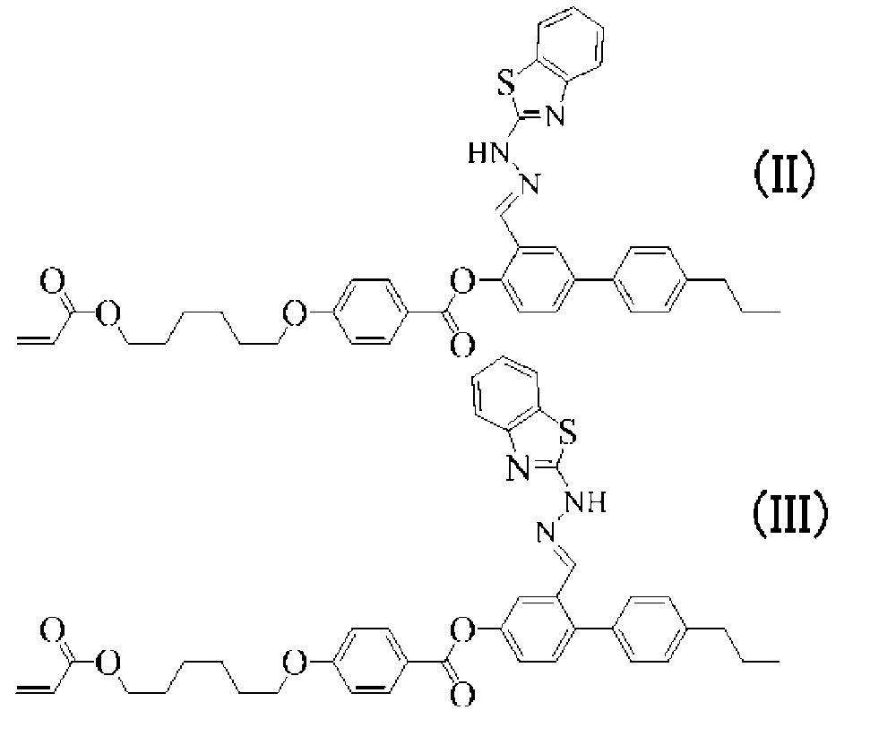
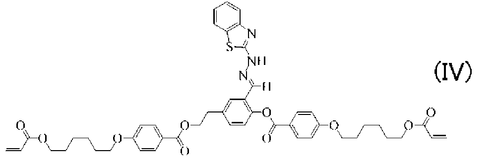
3-1.位相差層の作製
式(II)で表される化合物55部、式(III)で表される化合物25部、式(IV)で表される化合物20部をシクロペンタノン(CPN)400部に加えた後、60℃に加温、撹拌して溶解させ、溶解が確認された後、室温に戻し、イルガキュア907(BASFジャパン株式会社製)3部、メガファックF-554(DIC株式会社製)0.2部、p-メトキシフェノール(MEHQ)0.1部を加えて、さらに撹拌を行い、溶液を得た。溶液は、透明で均一であった。得られた溶液を0.20μmのメンブランフィルターでろ過し、重合性組成物を得た。一方、配向膜用ポリイミド溶液を厚さ0.7mmのガラス基材にスピンコート法を用いて塗布し、100℃で10分乾燥した後、200℃で60分焼成することにより塗膜を得た。得られた塗膜をラビング処理し、配向膜を形成した。ラビング処理は、市販のラビング装置を用いて行った。基材(実質的には、配向膜)に、上記で得られた重合性組成物をスピンコート法で塗布し、100℃で2分乾燥した。得られた塗布膜を室温まで冷却した後、高圧水銀ランプを用いて、30mW/cm2の強度で30秒間紫外線を照射して液晶配向固化層を得た。液晶配向固化層の厚みは2.8μmであり、面内位相差Re(550)は130nmであった。また、液晶配向固化層のRe(450)/Re(550)は0.851であり、逆分散波長特性を示した。この液晶配向固化層を位相差層とした。
3-2.ポジティブCプレートの作製
下記化学式(I)(式中の数字65および35はモノマーユニットのモル%を示し、便宜的にブロックポリマー体で表している:重量平均分子量5000)で示される側鎖型液晶ポリマー20重量部、ネマチック液晶相を示す重合性液晶(BASF社製:商品名PaliocolorLC242)80重量部および光重合開始剤(チバスペシャリティーケミカルズ社製:商品名イルガキュア907)5重量部をシクロペンタノン200重量部に溶解して液晶塗工液を調製した。そして、基材フィルム(ノルボルネン系樹脂フィルム:日本ゼオン(株)製、商品名「ゼオネックス」)に当該塗工液をバーコーターにより塗工した後、80℃で4分間加熱乾燥することによって液晶を配向させた。この液晶層に紫外線を照射し、液晶層を硬化させることにより、基材上に別の位相差層となる液晶配向固化層(ポジティブCプレート、厚み3μm)を形成した。この層のRe(590)は0nm、Rth(590)は-100nmであり、nz>nx=nyの屈折率特性を示した。
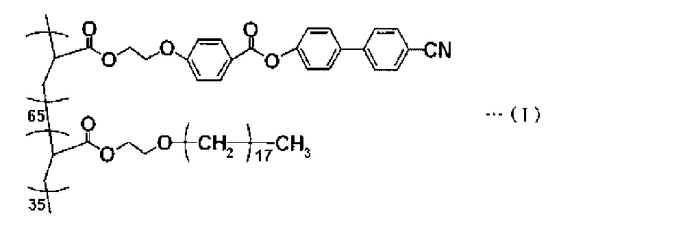
下記化学式(I)(式中の数字65および35はモノマーユニットのモル%を示し、便宜的にブロックポリマー体で表している:重量平均分子量5000)で示される側鎖型液晶ポリマー20重量部、ネマチック液晶相を示す重合性液晶(BASF社製:商品名PaliocolorLC242)80重量部および光重合開始剤(チバスペシャリティーケミカルズ社製:商品名イルガキュア907)5重量部をシクロペンタノン200重量部に溶解して液晶塗工液を調製した。そして、基材フィルム(ノルボルネン系樹脂フィルム:日本ゼオン(株)製、商品名「ゼオネックス」)に当該塗工液をバーコーターにより塗工した後、80℃で4分間加熱乾燥することによって液晶を配向させた。この液晶層に紫外線を照射し、液晶層を硬化させることにより、基材上に別の位相差層となる液晶配向固化層(ポジティブCプレート、厚み3μm)を形成した。この層のRe(590)は0nm、Rth(590)は-100nmであり、nz>nx=nyの屈折率特性を示した。
3-3.位相差層付偏光板の作製
上記2.で得られた偏光板の第2の接着層表面に上記3-1で得られた液晶配向固化層を転写し、さらに、液晶配向固化層表面に紫外線硬化型接着剤を介して上記3-2で得られたポジティブCプレートを転写し、視認側保護層(HC-TACフィルム)/第1の接着層(接着剤A)/偏光子/第2の接着層(粘着剤C)/位相差層/接着剤/ポジティブCプレートの構成を有する位相差層付偏光板を得た。得られた位相差層付偏光板を上記(3)の評価に供した。結果を表1に示す。
上記2.で得られた偏光板の第2の接着層表面に上記3-1で得られた液晶配向固化層を転写し、さらに、液晶配向固化層表面に紫外線硬化型接着剤を介して上記3-2で得られたポジティブCプレートを転写し、視認側保護層(HC-TACフィルム)/第1の接着層(接着剤A)/偏光子/第2の接着層(粘着剤C)/位相差層/接着剤/ポジティブCプレートの構成を有する位相差層付偏光板を得た。得られた位相差層付偏光板を上記(3)の評価に供した。結果を表1に示す。
[実施例2]
第2の接着層(粘着剤C)の厚みを5μmから30μmに変更したこと以外は実施例1と同様にして位相差層付偏光板を得た。得られた位相差層付偏光板を実施例1と同様の評価に供した。結果を表1に示す。
第2の接着層(粘着剤C)の厚みを5μmから30μmに変更したこと以外は実施例1と同様にして位相差層付偏光板を得た。得られた位相差層付偏光板を実施例1と同様の評価に供した。結果を表1に示す。
[実施例3]
第1の接着層として製造例1で得られた接着剤Aの代わりに製造例2で得られた接着剤Bを用いたこと以外は実施例1と同様にして位相差層付偏光板を得た。得られた位相差層付偏光板を実施例1と同様の評価に供した。結果を表1に示す。
第1の接着層として製造例1で得られた接着剤Aの代わりに製造例2で得られた接着剤Bを用いたこと以外は実施例1と同様にして位相差層付偏光板を得た。得られた位相差層付偏光板を実施例1と同様の評価に供した。結果を表1に示す。
[実施例4~12および比較例1~6]
視認側保護層、第1の接着層および第2の接着層を表1に示すように組み合わせて位相差層付偏光板を得た。得られた位相差層付偏光板を実施例1と同様の評価に供した。結果を表1に示す。
視認側保護層、第1の接着層および第2の接着層を表1に示すように組み合わせて位相差層付偏光板を得た。得られた位相差層付偏光板を実施例1と同様の評価に供した。結果を表1に示す。
表1において、HC-TACは上記のHC-TACフィルム;HC-COPは、シクロオレフィン系樹脂(COP)フィルム(厚み25μm)にHC層(厚み2μm)が形成されたフィルム;アクリルは、アクリル系樹脂フィルム;市販UVは、市販の紫外線硬化型接着剤;を示す。
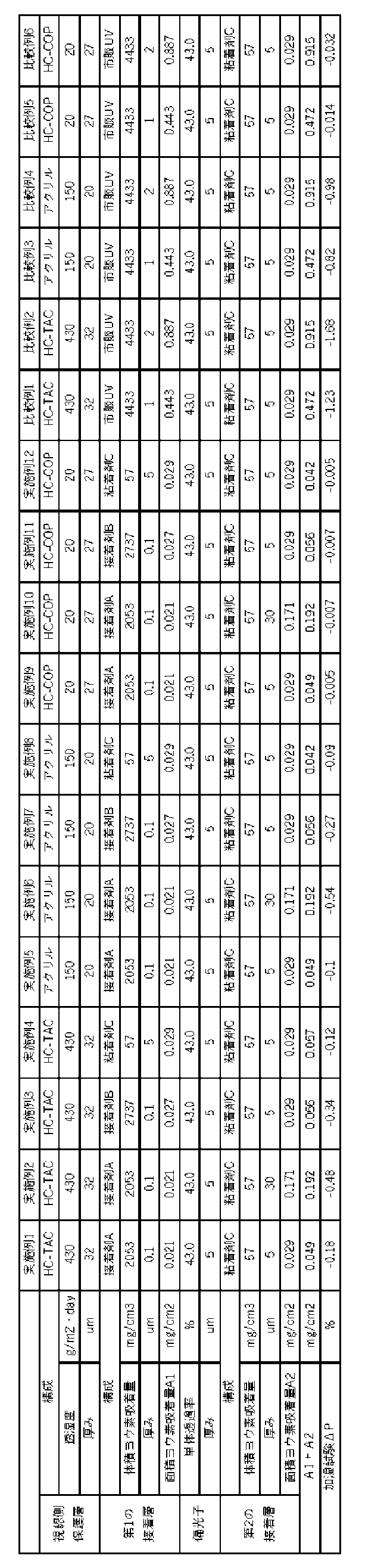
[評価]
表1から明らかなように、本発明の実施例によれば、第1の接着層の単位面積あたりのヨウ素吸着量A1と第2の接着層の単位面積あたりのヨウ素吸着量A2との合計を所定値以下とすることにより、薄型で、かつ、高温高湿環境下における偏光度の低下が抑制された偏光板および位相差層付偏光板を実現することができる。
表1から明らかなように、本発明の実施例によれば、第1の接着層の単位面積あたりのヨウ素吸着量A1と第2の接着層の単位面積あたりのヨウ素吸着量A2との合計を所定値以下とすることにより、薄型で、かつ、高温高湿環境下における偏光度の低下が抑制された偏光板および位相差層付偏光板を実現することができる。
本発明の偏光板および位相差層付偏光板は、液晶表示装置、有機EL表示装置および無機EL表示装置用の円偏光板として好適に用いられる。
10 偏光子
20 保護層
31 第1の接着層
32 第2の接着層
100 偏光板
120 位相差層
121 第1の位相差層
122 第2の位相差層
140 粘着剤層
200 位相差層付偏光板
20 保護層
31 第1の接着層
32 第2の接着層
100 偏光板
120 位相差層
121 第1の位相差層
122 第2の位相差層
140 粘着剤層
200 位相差層付偏光板
Claims (10)
- 偏光子と、該偏光子の視認側に第1の接着層を介して貼り合わせられた保護層と、該偏光子の該第1の接着層と反対側に配置された第2の接着層と、を含み、
該第1の接着層の単位面積あたりのヨウ素吸着量A1および該第2の接着層の単位面積あたりのヨウ素吸着量A2が下記式(1)を満足する、偏光板:
(A1+A2)<0.300(mg/cm2) ・・・(1)。 - 前記A1および前記A2がいずれも0.200mg/cm2以下である、請求項1に記載の偏光板。
- 前記第1の接着層および/または前記第2の接着層の厚みが0.3μm以下である、請求項1または2に記載の偏光板。
- 前記偏光子の厚みが10μm以下である、請求項1から3のいずれかに記載の偏光板。
- 前記偏光子の単体透過率が40.0%~45.0%である、請求項1から4のいずれかに記載の偏光板。
- 請求項1から5のいずれかに記載の偏光板と、
該偏光板に前記第2の接着層を介して貼り合わせられた、円偏光機能または楕円偏光機能を有する位相差層と、
を有する、位相差層付偏光板。 - 前記位相差層が液晶化合物の配向固化層である、請求項6に記載の位相差層付偏光板。
- 前記位相差層が単一層であり、
該位相差層のRe(550)が100nm~190nmであり、Re(450)/Re(550)が0.8~0.95であり、その遅相軸と前記偏光子の吸収軸とのなす角度が40°~50°である、
請求項6または7に記載の位相差層付偏光板。 - 前記位相差層が、第1の位相差層と第2の位相差層とを有し、
該第1の位相差層のRe(550)が200nm~300nmであり、その遅相軸と前記偏光子の吸収軸とのなす角度が10°~20°であり、
該第2の位相差層のRe(550)が100nm~190nmであり、その遅相軸と該偏光子の吸収軸とのなす角度が70°~80°である、
請求項6または7に記載の位相差層付偏光板。 - 請求項1から5のいずれかに記載の偏光板または請求項6から9のいずれかに記載の位相差層付偏光板を備える、画像表示装置。
Priority Applications (2)
| Application Number | Priority Date | Filing Date | Title |
|---|---|---|---|
| KR1020237005072A KR20230056666A (ko) | 2020-08-31 | 2021-06-16 | 편광판, 위상차층 부착 편광판 및 화상 표시 장치 |
| CN202180053545.7A CN115997160A (zh) | 2020-08-31 | 2021-06-16 | 偏光板、带相位差层的偏光板和图像显示装置 |
Applications Claiming Priority (2)
| Application Number | Priority Date | Filing Date | Title |
|---|---|---|---|
| JP2020145335A JP2022040566A (ja) | 2020-08-31 | 2020-08-31 | 偏光板、位相差層付偏光板および画像表示装置 |
| JP2020-145335 | 2020-08-31 |
Publications (1)
| Publication Number | Publication Date |
|---|---|
| WO2022044500A1 true WO2022044500A1 (ja) | 2022-03-03 |
Family
ID=80354973
Family Applications (1)
| Application Number | Title | Priority Date | Filing Date |
|---|---|---|---|
| PCT/JP2021/022888 Ceased WO2022044500A1 (ja) | 2020-08-31 | 2021-06-16 | 偏光板、位相差層付偏光板および画像表示装置 |
Country Status (5)
| Country | Link |
|---|---|
| JP (2) | JP2022040566A (ja) |
| KR (1) | KR20230056666A (ja) |
| CN (1) | CN115997160A (ja) |
| TW (1) | TW202216427A (ja) |
| WO (1) | WO2022044500A1 (ja) |
Families Citing this family (1)
| Publication number | Priority date | Publication date | Assignee | Title |
|---|---|---|---|---|
| TW202509539A (zh) * | 2023-07-26 | 2025-03-01 | 日商日東電工股份有限公司 | 光學積層體及使用該光學積層體之影像顯示裝置 |
Citations (5)
| Publication number | Priority date | Publication date | Assignee | Title |
|---|---|---|---|---|
| JP2007277510A (ja) * | 2006-03-15 | 2007-10-25 | Nitto Denko Corp | 粘着型光学フィルム、積層光学フィルムおよび画像表示装置 |
| JP2009042455A (ja) * | 2007-08-08 | 2009-02-26 | Nitto Denko Corp | 偏光板、その製造方法、光学フィルムおよび画像表示装置 |
| JP2009042457A (ja) * | 2007-08-08 | 2009-02-26 | Nitto Denko Corp | 偏光板、その製造方法、光学フィルムおよび画像表示装置 |
| JP2017102443A (ja) * | 2015-11-20 | 2017-06-08 | 日東電工株式会社 | 光学積層体および該光学積層体を用いた有機エレクトロルミネセンス表示装置 |
| JP2018205663A (ja) * | 2017-06-09 | 2018-12-27 | 日東電工株式会社 | 位相差層付偏光板および画像表示装置 |
Family Cites Families (19)
| Publication number | Priority date | Publication date | Assignee | Title |
|---|---|---|---|---|
| CA2316828C (en) | 1998-10-30 | 2010-02-23 | Teijin Limited | Retardation film and optical device employing it |
| JP4039682B2 (ja) * | 2006-06-09 | 2008-01-30 | 日東電工株式会社 | 偏光板用接着剤、偏光板、その製造方法、光学フィルムおよび画像表示装置 |
| JP4402096B2 (ja) * | 2006-11-15 | 2010-01-20 | 日東電工株式会社 | 偏光板、その製造方法、光学フィルムおよび画像表示装置 |
| JP5167059B2 (ja) * | 2007-10-02 | 2013-03-21 | 日東電工株式会社 | 偏光板、光学フィルムおよび画像表示装置 |
| JP4803833B2 (ja) * | 2007-10-05 | 2011-10-26 | 日東電工株式会社 | 偏光板の製造方法、偏光板、光学フィルムおよび画像表示装置 |
| JP5204608B2 (ja) * | 2007-10-10 | 2013-06-05 | 日東電工株式会社 | 偏光板、光学フィルムおよび画像表示装置 |
| KR101161600B1 (ko) * | 2007-10-22 | 2012-07-03 | 가부시키가이샤 닛폰 쇼쿠바이 | 편광판, 그 제조 방법, 광학 필름 및 화상 표시 장치 |
| JP2009134121A (ja) * | 2007-11-30 | 2009-06-18 | Nitto Denko Corp | 偏光板、光学フィルムおよび画像表示装置 |
| JP2009134136A (ja) * | 2007-11-30 | 2009-06-18 | Nitto Denko Corp | 偏光板、光学フィルムおよび画像表示装置 |
| JP5231181B2 (ja) * | 2007-11-30 | 2013-07-10 | 日東電工株式会社 | 偏光板、その製造方法、光学フィルムおよび画像表示装置 |
| JP2009139585A (ja) * | 2007-12-05 | 2009-06-25 | Nitto Denko Corp | 偏光板、光学フィルムおよび画像表示装置 |
| JP2009139510A (ja) * | 2007-12-05 | 2009-06-25 | Nitto Denko Corp | 偏光板の製造方法、偏光板及び液晶表示装置 |
| JP5167083B2 (ja) * | 2007-12-06 | 2013-03-21 | 日東電工株式会社 | 偏光板、その製造方法、光学フィルムおよび画像表示装置 |
| JP4870653B2 (ja) * | 2007-12-06 | 2012-02-08 | 日東電工株式会社 | 偏光板、その製造方法、光学フィルムおよび画像表示装置 |
| JP2009139723A (ja) * | 2007-12-07 | 2009-06-25 | Nitto Denko Corp | 偏光板、その製造方法、光学フィルムおよび画像表示装置 |
| JP2009139749A (ja) * | 2007-12-07 | 2009-06-25 | Nitto Denko Corp | 偏光板、その製造方法、光学フィルムおよび画像表示装置 |
| JP2009139720A (ja) * | 2007-12-07 | 2009-06-25 | Nitto Denko Corp | 偏光板、その製造方法、光学フィルムおよび画像表示装置 |
| JP2009139744A (ja) * | 2007-12-07 | 2009-06-25 | Nitto Denko Corp | 偏光板、その製造方法、光学フィルムおよび画像表示装置 |
| JP2009139741A (ja) * | 2007-12-07 | 2009-06-25 | Nitto Denko Corp | 偏光板、光学フィルムおよび画像表示装置 |
-
2020
- 2020-08-31 JP JP2020145335A patent/JP2022040566A/ja active Pending
-
2021
- 2021-06-16 CN CN202180053545.7A patent/CN115997160A/zh active Pending
- 2021-06-16 KR KR1020237005072A patent/KR20230056666A/ko active Pending
- 2021-06-16 WO PCT/JP2021/022888 patent/WO2022044500A1/ja not_active Ceased
- 2021-08-26 TW TW110131618A patent/TW202216427A/zh unknown
-
2024
- 2024-09-12 JP JP2024158350A patent/JP2024163298A/ja active Pending
Patent Citations (5)
| Publication number | Priority date | Publication date | Assignee | Title |
|---|---|---|---|---|
| JP2007277510A (ja) * | 2006-03-15 | 2007-10-25 | Nitto Denko Corp | 粘着型光学フィルム、積層光学フィルムおよび画像表示装置 |
| JP2009042455A (ja) * | 2007-08-08 | 2009-02-26 | Nitto Denko Corp | 偏光板、その製造方法、光学フィルムおよび画像表示装置 |
| JP2009042457A (ja) * | 2007-08-08 | 2009-02-26 | Nitto Denko Corp | 偏光板、その製造方法、光学フィルムおよび画像表示装置 |
| JP2017102443A (ja) * | 2015-11-20 | 2017-06-08 | 日東電工株式会社 | 光学積層体および該光学積層体を用いた有機エレクトロルミネセンス表示装置 |
| JP2018205663A (ja) * | 2017-06-09 | 2018-12-27 | 日東電工株式会社 | 位相差層付偏光板および画像表示装置 |
Also Published As
| Publication number | Publication date |
|---|---|
| CN115997160A (zh) | 2023-04-21 |
| KR20230056666A (ko) | 2023-04-27 |
| TW202216427A (zh) | 2022-05-01 |
| JP2024163298A (ja) | 2024-11-21 |
| JP2022040566A (ja) | 2022-03-11 |
Similar Documents
| Publication | Publication Date | Title |
|---|---|---|
| CN101542364B (zh) | 液晶显示装置及层叠偏振板以及偏振光光源装置 | |
| JP7046127B2 (ja) | 光学積層体および該光学積層体の位相差層付偏光板を含む画像表示装置 | |
| JP7648407B2 (ja) | 円偏光板およびそれを用いた画像表示装置 | |
| WO2021024544A1 (ja) | 位相差層付偏光板およびそれを用いた画像表示装置 | |
| WO2023084838A1 (ja) | 位相差層付偏光板および該位相差層付偏光板を含む画像表示装置 | |
| JP6900213B2 (ja) | 反射防止層および映り込み防止層付偏光板およびその製造方法 | |
| JP2024103763A (ja) | 偏光板、位相差層付偏光板および有機エレクトロルミネセンス表示装置 | |
| WO2021220729A1 (ja) | 偏光板および光学機能層付偏光板 | |
| JP2024163298A (ja) | 偏光板、位相差層付偏光板および画像表示装置 | |
| KR20230145479A (ko) | 위상차층 부착 편광판 및 그의 제조 방법, 및 해당 위상차층 부착 편광판을 이용한 화상 표시 장치 | |
| JP2022037502A (ja) | 位相差層付偏光板および画像表示装置 | |
| JP6699514B2 (ja) | Ipsモード用の偏光板のセット及びそれを用いたipsモード液晶表示装置 | |
| KR20230038790A (ko) | 원편광판, 유기 일렉트로 루미네선스 표시 장치, 표시 장치 | |
| JP7411520B2 (ja) | 偏光板、位相差層付偏光板および有機エレクトロルミネセンス表示装置 | |
| TW202122275A (zh) | 偏光板、偏光板之組合件及影像顯示裝置 | |
| JP2025164931A (ja) | 光学積層体および該光学積層体を用いた画像表示装置 | |
| WO2023084837A1 (ja) | 位相差層付偏光板および該位相差層付偏光板を含む画像表示装置 | |
| WO2023047748A1 (ja) | 位相差層付偏光板およびそれを用いた画像表示装置、ならびに、位相差層付偏光板の評価方法 | |
| WO2022091471A1 (ja) | 位相差層付偏光板および画像表示装置 | |
| JP2022141116A (ja) | 位相差層付偏光板 | |
| TW202122182A (zh) | 偏光板、偏光板之組合件及影像顯示裝置 |
Legal Events
| Date | Code | Title | Description |
|---|---|---|---|
| 121 | Ep: the epo has been informed by wipo that ep was designated in this application |
Ref document number: 21860931 Country of ref document: EP Kind code of ref document: A1 |
|
| NENP | Non-entry into the national phase |
Ref country code: DE |
|
| 122 | Ep: pct application non-entry in european phase |
Ref document number: 21860931 Country of ref document: EP Kind code of ref document: A1 |