WO2022038646A1 - 移相器及びフェーズドアレーアンテナ装置 - Google Patents
移相器及びフェーズドアレーアンテナ装置 Download PDFInfo
- Publication number
- WO2022038646A1 WO2022038646A1 PCT/JP2020/030932 JP2020030932W WO2022038646A1 WO 2022038646 A1 WO2022038646 A1 WO 2022038646A1 JP 2020030932 W JP2020030932 W JP 2020030932W WO 2022038646 A1 WO2022038646 A1 WO 2022038646A1
- Authority
- WO
- WIPO (PCT)
- Prior art keywords
- capacitor
- inductor
- pass
- filter
- pass filter
- Prior art date
- Legal status (The legal status is an assumption and is not a legal conclusion. Google has not performed a legal analysis and makes no representation as to the accuracy of the status listed.)
- Ceased
Links
Images



Classifications
-
- H—ELECTRICITY
- H03—ELECTRONIC CIRCUITRY
- H03H—IMPEDANCE NETWORKS, e.g. RESONANT CIRCUITS; RESONATORS
- H03H7/00—Multiple-port networks comprising only passive electrical elements as network components
- H03H7/18—Networks for phase shifting
- H03H7/19—Two-port phase shifters providing a predetermined phase shift, e.g. "all-pass" filters
-
- H—ELECTRICITY
- H01—ELECTRIC ELEMENTS
- H01P—WAVEGUIDES; RESONATORS, LINES, OR OTHER DEVICES OF THE WAVEGUIDE TYPE
- H01P1/00—Auxiliary devices
- H01P1/18—Phase-shifters
-
- H—ELECTRICITY
- H01—ELECTRIC ELEMENTS
- H01Q—ANTENNAS, i.e. RADIO AERIALS
- H01Q3/00—Arrangements for changing or varying the orientation or the shape of the directional pattern of the waves radiated from an antenna or antenna system
- H01Q3/24—Arrangements for changing or varying the orientation or the shape of the directional pattern of the waves radiated from an antenna or antenna system varying the orientation by switching energy from one active radiating element to another, e.g. for beam switching
Definitions
- the present disclosure relates to a phase shifter and a phased array antenna device including a phase shifter.
- a phased array antenna device is generally equipped with a phase shifter capable of changing the phase of a signal.
- the phase shifter is connected to an antenna element included in the phased array antenna device.
- the following Non-Patent Document 1 discloses a phase shifter in which the phase difference between the pass phase of the first path and the pass phase of the second path is the phase shift amount.
- a circuit in which a plurality of first pass-through filters are connected in series is inserted in the first path, and a circuit in which a plurality of second pass-through filters are connected in series in the second path. Is inserted.
- the first all-pass filter includes two inductors and two capacitors as lumped constant elements.
- the second all-pass filter also includes two inductors and two capacitors as lumped constant elements.
- phase shifter disclosed in Non-Patent Document 1
- the combination of lumped constant elements that realize the phase shift amount and the matching condition is uniquely determined, and the frequency characteristic of the phase shift amount is also uniquely determined. Therefore, there is a problem that the phase shift error is uniquely determined in a desired frequency band, and a desired phase shift amount may not be obtained.
- the present disclosure has been made to solve the above-mentioned problems, and an object of the present disclosure is to obtain a phase shifter capable of realizing a frequency characteristic of a desired phase shift amount in a desired frequency band.
- the phase shifter includes a first full-pass filter containing a plurality of elements, a second full-pass filter containing a plurality of elements, a first full-pass filter, or a second full-pass filter.
- a first selector switch that gives a signal to either one of the full-passing filters of the above, and a second that selects a signal that has passed through the first full-passing filter or a signal that has passed through the second full-passing filter.
- a changeover switch is provided, the first pass-through filter includes two inductors and three capacitors as multiple elements, and the second pass-through filter has two inductors and three capacitors as multiple elements.
- the first full range filter contains three inductors and two capacitors as multiple elements
- the second full pass filter contains three inductors and two capacitors as multiple elements. Two capacitors are included, and the element values of the plurality of elements included in the first full-range pass filter and the element values of the plurality of elements included in the second full-range pass filter realize impedance matching. It is determined by the impedance, signal frequency and variables.
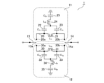
- FIG. It is a block diagram which shows the phase shifter 1 which concerns on Embodiment 1.
- FIG. It is explanatory drawing which shows the simulation result of the phase shift amount ⁇ of the phase shift device 1 shown in FIG.
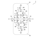
- FIG. It is a block diagram which shows the phase shifter 1 which concerns on Embodiment 2.
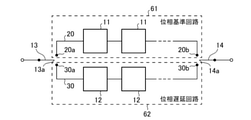
- FIG. It is a block diagram which shows the phase shifter 1 which concerns on Embodiment 3.
- the simulation result of the phase shift amount ⁇ when the phase reference circuit 61 includes only one first whole area pass filter 11 and the phase delay circuit 62 has only one second whole area pass filter 12 is shown.
- It is explanatory drawing. It is explanatory drawing which shows the simulation result of the phase shift amount ⁇ of the phase shift device 1 shown in FIG.
- FIG. It is a block diagram which shows the phase shifter 1 which concerns on Embodiment 4.
- FIG. It is a block diagram which shows the phased array antenna apparatus which concerns on Embodiment 5.
- FIG. 1 is a configuration diagram showing a phase shifter 1 according to the first embodiment.
- the phase shifter 1 includes a first all-pass filter 11, a second all-pass filter 12, a first changeover switch 13, and a second changeover switch 14.
- the first all-pass filter 11 includes two inductors and three capacitors as a plurality of elements. That is, the first pass-through filter 11 includes a first inductor 21, a second inductor 24, a first capacitor 22, a second capacitor 23, and a third capacitor 25 as a plurality of elements.
- the pass phase ⁇ 1 of the first full-range pass filter 11 is determined by the element values of the first inductor 21, the second inductor 24, the first capacitor 22, the second capacitor 23, and the third capacitor 25, respectively. ..
- the second all-pass filter 12 includes two inductors and three capacitors as a plurality of elements. That is, the second pass-through filter 12 includes a third inductor 31, a fourth inductor 34, a fourth capacitor 32, a fifth capacitor 33, and a sixth capacitor 35 as a plurality of elements.
- the pass phase ⁇ 2 of the second full-range pass filter 12 is determined by the element values of the third inductor 31, the fourth inductor 34, the fourth capacitor 32, the fifth capacitor 33, and the sixth capacitor 35, respectively. ..
- the connection terminal 13a of the first changeover switch 13 is connected to either one end 20a of the first path 20 or one end 30a of the second path 30.
- the first changeover switch 13 gives a signal to either the first whole-pass filter 11 or the second pass-through filter 12. That is, the first changeover switch 13 gives a signal to the first whole area pass filter 11 when the connection terminal 13a is connected to one end 20a of the first path 20.
- the first changeover switch 13 gives a signal to the second whole area pass filter 12 when the connection terminal 13a is connected to one end 30a of the second path 30.
- the connection terminal 14a of the second changeover switch 14 is connected to either the other end 20b of the first path 20 or the other end 30b of the second path 30.
- the second changeover switch 14 selects a signal that has passed through the first full-range pass filter 11 or a signal that has passed through the second full-range pass filter 12. That is, in the second changeover switch 14, the connection terminal 13a of the first changeover switch 13 is connected to one end 20a of the first path 20, and the connection terminal 14a is connected to the other end 20b of the first path 20. At that time, the signal that has passed through the first whole area passing filter 11 is selected.
- connection terminal 13a of the first changeover switch 13 When the connection terminal 13a of the first changeover switch 13 is connected to one end 20a of the first path 20 and the connection terminal 14a is connected to the other end 30b of the second path 30 in the second changeover switch 14. , Select the signal that has passed through the second full range filter 12.
- the first path 20 is a path connecting the first changeover switch 13 and the second changeover switch 14.
- a first inductor 21 is inserted in the first path 20.
- the second path 30 is a path connecting the first changeover switch 13 and the second changeover switch 14.
- a third inductor 31 is inserted in the second path 30.
- One end 20a of the first path 20 or one end 30a of the second path 30 is connected to the connection terminal 13a of the first changeover switch 13.
- the other end 20b of the first path 20 or the other end 30b of the second path 30 is connected to the connection terminal 14a of the second changeover switch 14.
- the first inductor 21 is inserted in the first path 20.
- the element value of the first inductor 21 is L 1r .
- One end of the first capacitor 22 is connected to one end of the first inductor 21.
- the other end of the first capacitor 22 is connected to the other end of the second capacitor 23 and one end of the second inductor 24, respectively.
- the element value of the first capacitor 22 is C 1r .
- One end of the second capacitor 23 is connected to the other end of the first inductor 21.
- the other end of the second capacitor 23 is connected to the other end of the first capacitor 22 and one end of the second inductor 24, respectively.
- the element value of the second capacitor 23 is C 1r .
- One end of the second inductor 24 is connected to the other ends of the first capacitor 22 and the second capacitor 23, respectively.
- the other end of the second inductor 24 is connected to one end of the third capacitor 25.
- the element value of the second inductor 24 is L 2r .
- One end of the third capacitor 25 is connected to the other end of the second inductor 24.
- the other end of the third capacitor 25 is grounded.
- the element value of the third capacitor 25 is C 2r .
- the third inductor 31 is inserted in the second path 30.
- the element value of the third inductor 31 is L 1p .
- One end of the fourth capacitor 32 is connected to one end of the third inductor 31.
- the other end of the fourth capacitor 32 is connected to the other end of the fifth capacitor 33 and one end of the fourth inductor 34, respectively.
- the element value of the fourth capacitor 32 is C 1p .
- One end of the fifth capacitor 33 is connected to the other end of the third inductor 31.
- the other end of the fifth capacitor 33 is connected to the other end of the fourth capacitor 32 and one end of the fourth inductor 34, respectively.
- the element value of the fifth capacitor 33 is C 1p .
- One end of the fourth inductor 34 is connected to the other end of each of the fourth capacitor 32 and the fifth capacitor 33.
- the other end of the fourth inductor 34 is connected to one end of the sixth capacitor 35.
- the element value of the fourth inductor 34 is L 2p .
- One end of the sixth capacitor 35 is connected to the other end of the fourth inductor 34.
- the other end of the sixth capacitor 35 is grounded.
- the element value of the sixth capacitor 35 is C 2p .
- the first pass-through filter 11 constitutes a phase reference circuit
- the second pass-through filter 12 constitutes a phase delay circuit.
- the phase shift amount ⁇ of the phase shifter 1 shown in FIG. 1 is determined by the phase difference between the pass phase ⁇ 1 of the first pass-through filter 11 and the pass phase ⁇ 2 of the second pass-through filter 12.
- connection terminal 13a of the first changeover switch 13 When the connection terminal 13a of the first changeover switch 13 is connected to one end 20a of the first path 20, for example, from a transmitter (not shown), the first whole area is passed through the first changeover switch 13. A signal is given to the filter 11.
- connection terminal 14a of the second changeover switch 14 When the connection terminal 14a of the second changeover switch 14 is connected to the other end 20b of the first path 20, the signal that has passed through the first whole area pass filter 11 is transmitted via the second changeover switch 14. For example, it is output to an antenna element (not shown).
- connection terminal 13a of the first changeover switch 13 When the connection terminal 13a of the first changeover switch 13 is connected to one end 30a of the second path 30, for example, from a transmitter (not shown), the second whole area is passed through the first changeover switch 13. A signal is given to the filter 12.
- connection terminal 14a of the second changeover switch 14 When the connection terminal 14a of the second changeover switch 14 is connected to the other end 30b of the second path 30, the signal that has passed through the second full-range passage filter 12 is transmitted via the second changeover switch 14. For example, it is output to an antenna element (not shown).
- the phase shifter 1 realizes both impedance matching with the antenna element and impedance matching with the transmitter.
- the element values of the plurality of elements included in the first full-range pass filter 11 and the element values of the plurality of elements included in the second full-range pass filter 12 are expressed by the following equation (1). ) Satisfies, impedance matching can be achieved at all frequencies.
- ⁇ 0 is the central angle frequency of each frequency band in the first whole area passing filter 11 and the second whole area passing filter 12, and ⁇ t and G are common to the respective element values. Is a variable of.
- the phase shift amount ⁇ of the phase shifter 1 shown in FIG. 1 is determined by the phase difference between the pass phase ⁇ 1 of the first pass filter 11 and the pass phase ⁇ 2 of the second pass filter 12, and has a central angle.
- the phase shift amount ⁇ 0 at the frequency ⁇ 0 is expressed by the following equation (2).
- each of ⁇ t and G is a free variable for changing the phase shift amount ⁇ 0 at the central angular frequency ⁇ 0 . Therefore, by changing ⁇ t or G, it is possible to change the phase shift amount ⁇ 0 at the central angular frequency ⁇ 0 while achieving matching at the impedance Z 0 .
- each of the first whole-pass filter and the second pass-through filter includes two inductors and two capacitors as a plurality of elements. If so, the phase shift amount ⁇ 0 at the central angular frequency ⁇ 0 is expressed by the following equation (3).
- one free variable for changing the phase shift amount ⁇ 0 at the central angular frequency ⁇ 0 is one of ⁇ t . If ⁇ t is determined, the combination of elements is uniquely determined, and the phase shift amount other than the central angular frequency ⁇ 0 is also uniquely determined, so that the frequency characteristic of the phase shift amount is uniquely determined. Therefore, there is little degree of freedom in design for widening the frequency band. Therefore, since the phase shift error is uniquely determined in the desired frequency band, the desired phase shift amount may not be obtained.
- the phase shifter 1 shown in FIG. 1 there are two free variables for changing the phase shift amount ⁇ , ⁇ t and G, and the frequency band is set higher than that of the phase shifter described in Non-Patent Document 1. There is a lot of design freedom to widen the bandwidth.
- FIG. 2 is an explanatory diagram showing a simulation result of the phase shift amount ⁇ of the phase shifter 1 shown in FIG.
- the phase shifter 1 is designed with the center frequency f 0 set to 5.0 [GHz] and the phase shift amount ⁇ 0 at the center frequency f 0 set to 90 [degrees].
- the variable G is changed as a free variable for changing the frequency characteristic of the phase shift amount ⁇ of the phase shifter 1.
- the first full-range pass filter 11 including a plurality of elements
- the second full-range pass filter 12 including a plurality of elements
- the first full-range pass filter 11 or the first full-range pass filter 11 or the like.
- the first global pass filter 11 includes, as a plurality of elements, two inductors and three capacitors
- the second global pass filter 12 has a plurality of elements.
- the elements include two inductors and three capacitors, and the element values of the plurality of elements included in the first full-range pass filter 11 and the plurality of elements included in the second full-range pass filter 12.
- the phase shifter 1 is configured so that the element value is determined by the impedance that realizes impedance matching, the frequency of the signal, and the variables. Therefore, the phase shifter 1 can realize the frequency characteristic of the desired phase shift amount in the desired frequency band.
- the first pass-through filter 15 includes three inductors and two capacitors as a plurality of elements
- the second pass-through filter 16 includes three inductors and two capacitors as a plurality of elements.
- the phase shifter 1 including two capacitors will be described.
- FIG. 3 is a block diagram showing the phase shifter 1 according to the second embodiment.
- the phase shifter 1 includes a first whole-pass filter 15, a second pass-through filter 16, a first changeover switch 13, and a second changeover switch 14.
- the first all-pass filter 15 includes three inductors and two capacitors as a plurality of elements. That is, the first pass-through filter 15 includes a first inductor 42, a second inductor 43, a third inductor 45, a first capacitor 41, and a second capacitor 44 as a plurality of elements.
- the pass phase ⁇ 1 of the first full-range pass filter 15 is determined by the element values of the first inductor 42, the second inductor 43, the third inductor 45, the first capacitor 41, and the second capacitor 44, respectively. ..
- the second all-pass filter 16 includes three inductors and two capacitors as a plurality of elements. That is, the second pass-through filter 16 includes a fourth inductor 52, a fifth inductor 53, a sixth inductor 55, a third capacitor 51, and a fourth capacitor 54 as a plurality of elements.
- the pass phase ⁇ 2 of the second full-range pass filter 16 is determined by the element values of the fourth inductor 52, the fifth inductor 53, the sixth inductor 55, the third capacitor 51, and the fourth capacitor 54, respectively. ..
- the first capacitor 41 is inserted in the first path 20.
- the element value of the first capacitor 41 is C 1r '.
- One end of the first inductor 42 is connected to one end of the first capacitor 41.
- the other end of the first inductor 42 is connected to the other end of the second inductor 43 and one end of the second capacitor 44, respectively.
- the element value of the first inductor 42 is L 1r '.
- One end of the second inductor 43 is connected to the other end of the first capacitor 41.
- the other end of the second inductor 43 is connected to the other end of the first inductor 42 and one end of the second capacitor 44, respectively.
- the element value of the second inductor 43 is L 1r '.
- One end of the second capacitor 44 is connected to the other end of each of the first inductor 42 and the second inductor 43.
- the other end of the second capacitor 44 is connected to one end of the third inductor 45.
- the element value of the second capacitor 44 is C 2r '.
- One end of the third inductor 45 is connected to the other end of the second capacitor 44.
- the other end of the third inductor 45 is grounded.
- the element value of the third inductor 45 is L 2r '.
- the third capacitor 51 is inserted in the second path 30.
- the element value of the third capacitor 51 is C 1p '.
- One end of the fourth inductor 52 is connected to one end of the third capacitor 51.
- the other end of the fourth inductor 52 is connected to the other end of the fifth inductor 53 and one end of the fourth capacitor 54, respectively.
- the element value of the fourth inductor 52 is L 1p '.
- One end of the fifth inductor 53 is connected to the other end of the third capacitor 51.
- the other end of the fifth inductor 53 is connected to the other end of the fourth inductor 52 and one end of the fourth capacitor 54, respectively.
- the element value of the fifth inductor 53 is L 1p '.
- One end of the fourth capacitor 54 is connected to the other end of each of the fourth inductor 52 and the fifth inductor 53.
- the other end of the fourth capacitor 54 is connected to one end of the sixth inductor 55.
- the element value of the fourth capacitor 54 is C 2p '.
- One end of the sixth inductor 55 is connected to the other end of the fourth capacitor 54.
- the other end of the sixth inductor 55 is grounded.
- the element value of the sixth inductor 55 is L 2p '.
- the first pass-through filter 15 constitutes a phase reference circuit
- the second pass-through filter 16 constitutes a phase delay circuit.
- the phase shift amount ⁇ of the phase shifter 1 shown in FIG. 3 is determined by the phase difference between the pass phase ⁇ 1 of the first pass-through filter 15 and the pass phase ⁇ 2 of the second pass-through filter 16.
- connection terminal 13a of the first changeover switch 13 When the connection terminal 13a of the first changeover switch 13 is connected to one end 20a of the first path 20, for example, from a transmitter (not shown), the first whole area is passed through the first changeover switch 13. A signal is given to the filter 15.
- connection terminal 14a of the second changeover switch 14 When the connection terminal 14a of the second changeover switch 14 is connected to the other end 20b of the first path 20, the signal that has passed through the first whole area pass filter 15 is transmitted via the second changeover switch 14. For example, it is output to an antenna element (not shown).
- connection terminal 13a of the first changeover switch 13 When the connection terminal 13a of the first changeover switch 13 is connected to one end 30a of the second path 30, for example, from a transmitter (not shown), the second whole area is passed through the first changeover switch 13. A signal is given to the filter 16.
- connection terminal 14a of the second changeover switch 14 When the connection terminal 14a of the second changeover switch 14 is connected to the other end 30b of the second path 30, the signal that has passed through the second full-range passage filter 16 passes through the second changeover switch 14. For example, it is output to an antenna element (not shown).
- the phase shifter 1 realizes both impedance matching with the antenna element and impedance matching with the transmitter.
- the element values of the plurality of elements included in the first full-range pass filter 15 and the element values of the plurality of elements included in the second full-range pass filter 16 are expressed by the following equation (4). ) Satisfies, impedance matching can be achieved at all frequencies.
- ⁇ 0 is the central angle frequency of each frequency band in the first whole area passing filter 15 and the second whole area passing filter 16, and ⁇ t and G are common to the respective element values. Is a variable of.
- the phase shift amount ⁇ of the phase shifter 1 shown in FIG. 3 is determined by the phase difference between the pass phase ⁇ 1 of the first pass-through filter 15 and the pass phase ⁇ 2 of the second pass-through filter 16 and has a central angle.
- the phase shift amount ⁇ 0 at the frequency ⁇ 0 is expressed by the following equation (5).
- each of ⁇ t and G is a free variable for changing the phase shift amount ⁇ 0 at the central angular frequency ⁇ 0 . Therefore, by changing ⁇ t or G, it is possible to change the phase shift amount ⁇ 0 at the central angular frequency ⁇ 0 while achieving matching at the impedance Z 0 .
- the first full-range pass filter 15 including a plurality of elements
- the second full-range pass filter 16 including a plurality of elements
- the first full-range pass filter 15, or the first full-pass filter 15 or the like A signal that has passed through the first changeover switch 13 and the first full-range pass filter 15 that gives a signal to either one of the second full-range pass filters 16, or a signal that has passed through the second full-range pass filter 16.
- the first global pass filter 15 includes, as a plurality of elements, three inductors and two capacitors
- the second global pass filter 16 has a plurality of elements.
- the elements include three inductors and two capacitors, and the element values of the plurality of elements included in the first full-range pass filter 15 and the plurality of elements included in the second full-range pass filter 16.
- the phase shifter 1 is configured so that the element value is determined by the impedance that realizes impedance matching, the frequency of the signal, and the variables. Therefore, the phase shifter 1 can realize the frequency characteristic of the desired phase shift amount in the desired frequency band.
- Embodiment 3 In the third embodiment, a plurality of first pass-through filters 11 inserted in the first path 20 are connected in series, and a second pass-through filter 12 inserted in the second path 30 is connected. A plurality of phase shifters 1 connected in series will be described.
- FIG. 4 is a configuration diagram showing the phase shifter 1 according to the third embodiment.
- the phase reference circuit 61 is provided between the first changeover switch 13 and the second changeover switch 14, and includes a plurality of first pass-through filters 11 shown in FIG.
- the plurality of first pass-through filters 11 are connected in series with each other.
- the phase reference circuit 61 includes a plurality of first pass-through filters 11.
- the phase reference circuit 61 may include a plurality of first whole-pass filters 15 shown in FIG. 3 instead of the first pass-through filter 11 shown in FIG.
- the phase delay circuit 62 is provided between the first changeover switch 13 and the second changeover switch 14, and includes a plurality of second pass-through filters 12 shown in FIG.
- the plurality of second pass-through filters 12 are connected in series with each other.
- the phase delay circuit 62 includes a plurality of second pass-through filters 12.
- the phase delay circuit 62 may include a plurality of second whole-pass filters 16 shown in FIG. 3 instead of the second pass-through filter 12 shown in FIG.
- the passing phase of the phase reference circuit 61 is the sum of the passing phases ⁇ 1 of the plurality of first global passing filters 11, and the passing phase of the phase delay circuit 62 is the passing phase ⁇ of the plurality of second global passing filters 12. It is the sum of two .
- the phase shift amount ⁇ of the phase shifter 1 shown in FIG. 4 is determined by the phase difference between the pass phase of the phase reference circuit 61 and the pass phase of the phase delay circuit 62.
- the phase reference circuit 61 includes only one first full-range pass filter 11 (hereinafter, referred to as “first-stage full-pass filter 11”), and the phase delay circuit 62 includes a phase delay circuit 62.
- first-stage full-pass filter 11 first full-range pass filter 11
- the phase delay circuit 62 includes a phase delay circuit 62.
- the phase reference circuit 61 includes two first all-pass filters 11 and the phase delay circuit 62 includes two second all-pass filters 12.
- the first whole area passing filter 11 from the first changeover switch 13 is the first whole area passing filter 11 in the first stage, and the first whole area from the first changeover switch 13 to the first whole area.
- the pass filter 11 is the first whole area pass filter 11 in the second stage.
- the second whole area passing filter 12 first from the first changeover switch 13 is the second whole area passing filter 12 in the first stage, and the second whole area passing from the first changeover switch 13 to the second whole area.
- the filter 12 is a second-stage full-range filter 12 in the second stage.
- the phase shift amount ⁇ by the first-stage first full-range pass filter 11 and the first-stage second full-range pass filter 12 is the phase shift amount ⁇ 0 at the center frequency f 0 .
- the phase shift amount ⁇ by the first full-range pass filter 11 in the second stage and the second full-range pass filter 12 in the second stage is the phase shift amount at the center frequency f0 .
- each element value is designed so that ⁇ 0 becomes 90 degrees and the phase shift amount ⁇ of the phase shifter 1 becomes the minimum value at the center frequency f 0 .
- the frequency dependence of the phase shift amount ⁇ by the first-stage first-range pass filter 11 and the first-stage second-stage pass-through filter 12 The frequency dependence of the phase shift amount ⁇ by the first full-range pass filter 11 in the second stage and the second full-range pass filter 12 in the second stage is compensated for each other. By compensating for the frequency dependence, the phase shift error of the phase shifter 1 is reduced.
- FIG. 6 is an explanatory diagram showing a simulation result of the phase shift amount ⁇ of the phase shifter 1 shown in FIG.
- the center frequency f 0 is 5.0 [GHz]
- G 1.010
- G 2.010
- G 3.010
- G 4.010
- G 5.010
- the first stage of the first stage by changing the variable G of the element values constituting the first whole area passing filter 11 of the second stage and the second whole area passing filter 12 of the second stage, the first stage of the first stage It can be seen that the frequency dependence of the phase shift amount in the whole area passing filter 11 of 1 and the second whole area passing filter 12 of the first stage is compensated, and the phase shift error of the phase shifter 1 is reduced.
- phase reference circuit 61 includes two first full-range pass filters 11, and the phase delay circuit 62 includes two second full-range pass filters 12, so that the first and second stages are transferred. It is assumed that both phases have a center frequency of f 0 and a phase shift amount of ⁇ 0 .
- the phase reference circuit 61 includes N first all-pass filters 11 and the phase delay circuit 62 includes N second all-pass filters 12, with a center frequency f 0 and a center frequency at each stage.
- the phase shift amount ⁇ 0 at f 0 may be different from each other in each stage.
- the frequency characteristic of the phase shift amount ⁇ of each stage may be composed only of those having a maximum value, or the frequency characteristic of the phase shift amount ⁇ of each stage may be composed only of those having a minimum value. May be good.
- the frequency characteristic of the phase shift amount ⁇ in each stage may be composed of a combination of one having a maximum value and one having a minimum value.
- the order of the columns of the N first pass-through filters 11 may be arbitrary, and the order of the columns of the N second pass-through filters 12 may be arbitrary.
- the phase reference circuit 61 includes a third whole area pass filter 17 in addition to the first whole area pass filter 11, and the phase delay circuit 62 is provided with the second whole area pass filter 12 in addition to the second whole area pass filter 12.
- the phase shifter 1 including the fourth all-pass filter 18 will be described.
- FIG. 7 is a block diagram showing the phase shifter 1 according to the fourth embodiment.
- the third pass-through filter 17 is connected in series with the first pass-through filter 11.
- the third all-pass filter 17 includes two inductors and two capacitors as a plurality of elements. That is, the third whole-pass filter 17 includes inductors 72, 73 and capacitors 71, 74 as a plurality of elements.
- the capacitor 71 is inserted in the first path 20.
- One end of the inductor 72 is connected to one end of the capacitor 71.
- the other end of the inductor 72 is connected to the other end of the inductor 73 and one end of the capacitor 74, respectively.
- One end of the inductor 73 is connected to the other end of the capacitor 71.
- the other end of the inductor 73 is connected to the other end of the inductor 72 and one end of the capacitor 74, respectively.
- One end of the capacitor 74 is connected to the other end of the inductor 72 and the other end of the inductor 73, respectively.
- the other end of the capacitor 74 is grounded.
- the fourth all-pass filter 18 is connected in series with the second all-pass filter 12.
- the fourth all-pass filter 18 includes two inductors and two capacitors as a plurality of elements. That is, the fourth all-pass filter 18 includes inductors 82, 83 and capacitors 81, 84 as a plurality of elements.
- the capacitor 81 is inserted in the second path 30.
- One end of the inductor 82 is connected to one end of the capacitor 81.
- the other end of the inductor 82 is connected to the other end of the inductor 83 and one end of the capacitor 84, respectively.
- One end of the inductor 83 is connected to the other end of the capacitor 81.
- the other end of the inductor 83 is connected to the other end of the inductor 82 and one end of the capacitor 84, respectively.
- One end of the capacitor 84 is connected to the other end of the inductor 82 and the other end of the inductor 83, respectively.
- the other end of the capacitor 84 is grounded.
- the phase reference circuit 61 includes a third whole-pass filter 17 in addition to the first pass-through filter 11, and the phase delay circuit 62 has a second pass-through filter 12.
- a fourth all-pass filter 18 is provided.
- the phase reference circuit 61 includes a third whole-pass filter 17 in addition to the first pass-through filter 15, and the phase delay circuit 62 is the second pass-through filter 16.
- a fourth all-pass filter 18 may be provided.
- the phase reference circuit 61 includes a third whole area pass filter 17 in addition to the first whole area pass filter 11 and the first whole area pass filter 15, and the phase delay circuit 62 includes a second whole area pass filter 12.
- a fourth whole-pass filter 18 may be provided.
- the third pass-through filter 17 corresponds to the first pass-through filter described in Non-Patent Document 1.
- the fourth whole area passing filter 18 corresponds to the second whole area passing filter described in Non-Patent Document 1. Therefore, in the phase shifter composed of only the third full-range pass filter 17 of the phase reference circuit 61 and the fourth full-range pass filter 18 of the phase delay circuit 62, the frequency characteristic of the phase shift amount is realized while achieving impedance matching. Cannot be changed. However, in the phase shifter 1 shown in FIG. 7, since the phase reference circuit 61 includes the first whole-pass filter 11 and the phase delay circuit 62 includes the second pass-through filter 12, impedance matching is performed. While achieving this, the amount of phase shift can be changed.
- the elements included in the third pass-through filter 17 are two inductors 72, 73 and two capacitors 71, 74, and the number of elements included in the third pass-through filter 17 is the first. It is less than the number of elements included in the whole area passing filter 11. Further, the elements included in the fourth full-range pass filter 18 are two inductors 82, 83 and two capacitors 81, 84, and the number of elements included in the fourth full-pass filter 18 is increased. It is less than the number of elements included in the second all-pass filter 12. Therefore, under the condition that the number of stages of the all-pass filter included in the phase reference circuit 61 is the same and the number of stages of the all-pass filter included in the phase delay circuit 62 is the same, the phase shifter shown in FIG. 1 can be made smaller than the phase shifter 1 shown in FIG.
- the third global pass filter 17 may include two inductors 72, 73 and two capacitors 71, 74, and two inductors 72, 73 and two capacitors 71. , 74, respectively, is not limited to the arrangement shown in FIG. In FIG. 7, for example, the inductor 72 is arranged at the position where the capacitor 71 is arranged, the inductor 73 is arranged at the position where the capacitor 74 is arranged, and the capacitor 71 is arranged at the position where the inductor 72 is arranged. , The capacitor 74 may be arranged at the position where the inductor 73 is arranged. In the phase shifter 1 shown in FIG.
- the fourth global pass filter 18 may include two inductors 82, 83 and two capacitors 81, 84, and two inductors 82, 83 and two capacitors 81. , 84, respectively, is not limited to the arrangement shown in FIG. In FIG. 7, for example, the inductor 82 is arranged at the position where the capacitor 81 is arranged, the inductor 83 is arranged at the position where the capacitor 84 is arranged, and the capacitor 81 is arranged at the position where the inductor 82 is arranged. , The capacitor 84 may be arranged at the position where the inductor 83 is arranged.
- Embodiment 5 A phased array antenna device including the phase shifter 1 according to any one of the first to fourth embodiments will be described.
- FIG. 8 is a configuration diagram showing a phased array antenna device according to the fifth embodiment.
- M is an integer of 2 or more.
- the phase shifter 92-m is the phase shifter 1 according to any one of the first to fourth embodiments.
- the phase shifter 92-m shifts the transmission signal output from the transmitter 91-m, and outputs the transmitted signal after the phase shift to the antenna element 93-m.
- the antenna element 93-m radiates radio waves related to the transmission signal after the phase shift by the phase shifter 92-m into space.
- the phased array antenna device shown in FIG. 8 radio waves related to transmission signals are radiated into space.
- the phased array antenna device may receive radio waves.
- the antenna element 93-m of the phased array antenna device receives radio waves
- the antenna element 93-m outputs the received signal of the radio waves to the phase shifter 92-m.
- the phase shifter 92-m shifts the received signal output from the antenna element 93-m, and outputs the received signal after the phase shift to a receiver (not shown).
- any combination of the embodiments can be freely combined, any component of the embodiment can be modified, or any component can be omitted in each embodiment.
- the present disclosure is suitable for phase shifters.
- the present disclosure is suitable for a phased array antenna device with a phase shifter.
Landscapes
- Filters And Equalizers (AREA)
- Waveguide Switches, Polarizers, And Phase Shifters (AREA)
- Variable-Direction Aerials And Aerial Arrays (AREA)
Priority Applications (4)
| Application Number | Priority Date | Filing Date | Title |
|---|---|---|---|
| PCT/JP2020/030932 WO2022038646A1 (ja) | 2020-08-17 | 2020-08-17 | 移相器及びフェーズドアレーアンテナ装置 |
| JP2022543816A JP7150223B2 (ja) | 2020-08-17 | 2020-08-17 | 移相器及びフェーズドアレーアンテナ装置 |
| EP20950212.9A EP4175056B1 (en) | 2020-08-17 | 2020-08-17 | Phase shifter and phased array antenna device |
| US18/079,377 US12323123B2 (en) | 2020-08-17 | 2022-12-12 | Phase shifter comprising selectable first and second all-pass filters, where the all-pass filters include capacitors and inductors of determined values to achieve impedance matching |
Applications Claiming Priority (1)
| Application Number | Priority Date | Filing Date | Title |
|---|---|---|---|
| PCT/JP2020/030932 WO2022038646A1 (ja) | 2020-08-17 | 2020-08-17 | 移相器及びフェーズドアレーアンテナ装置 |
Related Child Applications (1)
| Application Number | Title | Priority Date | Filing Date |
|---|---|---|---|
| US18/079,377 Continuation US12323123B2 (en) | 2020-08-17 | 2022-12-12 | Phase shifter comprising selectable first and second all-pass filters, where the all-pass filters include capacitors and inductors of determined values to achieve impedance matching |
Publications (1)
| Publication Number | Publication Date |
|---|---|
| WO2022038646A1 true WO2022038646A1 (ja) | 2022-02-24 |
Family
ID=80322869
Family Applications (1)
| Application Number | Title | Priority Date | Filing Date |
|---|---|---|---|
| PCT/JP2020/030932 Ceased WO2022038646A1 (ja) | 2020-08-17 | 2020-08-17 | 移相器及びフェーズドアレーアンテナ装置 |
Country Status (4)
| Country | Link |
|---|---|
| US (1) | US12323123B2 (https=) |
| EP (1) | EP4175056B1 (https=) |
| JP (1) | JP7150223B2 (https=) |
| WO (1) | WO2022038646A1 (https=) |
Families Citing this family (1)
| Publication number | Priority date | Publication date | Assignee | Title |
|---|---|---|---|---|
| CN116762275A (zh) * | 2021-02-12 | 2023-09-15 | 株式会社村田制作所 | 分配器以及通信装置 |
Citations (3)
| Publication number | Priority date | Publication date | Assignee | Title |
|---|---|---|---|---|
| JP2002076810A (ja) * | 2000-08-31 | 2002-03-15 | Mitsubishi Electric Corp | 移相器 |
| JP2013098744A (ja) * | 2011-10-31 | 2013-05-20 | Sumitomo Electric Device Innovations Inc | 移相器およびその設計方法 |
| CN107332538A (zh) * | 2017-06-27 | 2017-11-07 | 中国科学院微电子研究所 | 一种数字移相器 |
Family Cites Families (7)
| Publication number | Priority date | Publication date | Assignee | Title |
|---|---|---|---|---|
| US5920241A (en) * | 1997-05-12 | 1999-07-06 | Emc Technology Llc | Passive temperature compensating LC filter |
| US7276993B2 (en) * | 2005-05-31 | 2007-10-02 | Agile Rf, Inc. | Analog phase shifter using cascaded voltage tunable capacitor |
| JP4963241B2 (ja) | 2007-02-23 | 2012-06-27 | 三菱電機株式会社 | 移相回路 |
| JP2011259215A (ja) * | 2010-06-09 | 2011-12-22 | Toshiba Corp | 移相器 |
| TWI536733B (zh) * | 2014-05-30 | 2016-06-01 | 國立臺灣大學 | 共模雜訊抑制裝置 |
| JP6566441B2 (ja) | 2016-01-07 | 2019-08-28 | 学校法人上智学院 | 移相器 |
| JP6808096B2 (ja) | 2018-06-19 | 2021-01-06 | 三菱電機株式会社 | 移相器 |
-
2020
- 2020-08-17 EP EP20950212.9A patent/EP4175056B1/en active Active
- 2020-08-17 JP JP2022543816A patent/JP7150223B2/ja active Active
- 2020-08-17 WO PCT/JP2020/030932 patent/WO2022038646A1/ja not_active Ceased
-
2022
- 2022-12-12 US US18/079,377 patent/US12323123B2/en active Active
Patent Citations (3)
| Publication number | Priority date | Publication date | Assignee | Title |
|---|---|---|---|---|
| JP2002076810A (ja) * | 2000-08-31 | 2002-03-15 | Mitsubishi Electric Corp | 移相器 |
| JP2013098744A (ja) * | 2011-10-31 | 2013-05-20 | Sumitomo Electric Device Innovations Inc | 移相器およびその設計方法 |
| CN107332538A (zh) * | 2017-06-27 | 2017-11-07 | 中国科学院微电子研究所 | 一种数字移相器 |
Non-Patent Citations (2)
| Title |
|---|
| XINYI TANG ET AL.: "Large Bandwidth Digital Phase Shifters With All- Pass, High-Pass, and Low-Pass Networks", IEEE TRANSACTIONS ON MICROWAVE THEORY AND TECHNIQUES, vol. 61, no. 6, 2013, pages 2325 - 2331, XP011511918, ISSN: 0018-9480, DOI: 10.1109/TMTT.2013.2260420 * |
| XINYI TANG ET AL.: "Large Bandwidth Digital Phase Shifters with All-pass, High-pass, and Low-pass Networks", IEEE TRANSACTIONS ON MTTS, vol. 61, June 2013 (2013-06-01), pages 2325 - 2331, XP011511918, DOI: 10.1109/TMTT.2013.2260420 |
Also Published As
| Publication number | Publication date |
|---|---|
| US20230106157A1 (en) | 2023-04-06 |
| US12323123B2 (en) | 2025-06-03 |
| JP7150223B2 (ja) | 2022-10-07 |
| EP4175056A4 (en) | 2023-08-02 |
| EP4175056B1 (en) | 2025-01-15 |
| EP4175056A1 (en) | 2023-05-03 |
| JPWO2022038646A1 (https=) | 2022-02-24 |
Similar Documents
| Publication | Publication Date | Title |
|---|---|---|
| US9438288B2 (en) | System providing reduced intermodulation distortion | |
| CN111771345B (zh) | 用于可配置混合自干扰消除的系统和方法 | |
| US10230348B2 (en) | Sub-network enhanced reflectionless filter topology | |
| US9712313B2 (en) | Systems for multi-peak-filter-based analog self-interference cancellation | |
| CN117220628B (zh) | 一种超宽带矢量调制移相器及相控阵系统 | |
| RU2676192C1 (ru) | Сверхширокополосный фиксированный фазовращатель, основанный на ёмкостной нагрузке | |
| US9628164B1 (en) | Beamforming engine | |
| CN103190076A (zh) | 可调谐滤波器设备和方法 | |
| WO2022038646A1 (ja) | 移相器及びフェーズドアレーアンテナ装置 | |
| CN114866071A (zh) | 一种w波段超高移相分辨率的移相器 | |
| US7633358B2 (en) | Phase shifter circuit with proper broadband performance | |
| JP6808096B2 (ja) | 移相器 | |
| US12218394B2 (en) | Power feed circuit comprising a synthesizing-distributing unit and a phase shifting unit configured for feeding a two point or a four point circularly polarized antenna | |
| JP7099628B2 (ja) | 移相器 | |
| WO2020240626A1 (ja) | 遅延回路及び線路切換型移相器 | |
| US9973166B2 (en) | Phase shift circuit | |
| JPWO2022038646A5 (https=) | ||
| JP5652185B2 (ja) | 群遅延時間調整回路および電力分配合成回路 | |
| JP4864758B2 (ja) | 直交ミクサおよびイメージリジェクションミクサ | |
| CN216390945U (zh) | 一种移相网络 | |
| JP2006237660A (ja) | アンテナ装置及びその利用方法 | |
| US6084890A (en) | Method and apparatus for combining carrier signals | |
| Jie et al. | Design of C-band 5 bit digital phase shifter based on CMOS technology | |
| JPH02210906A (ja) | 移相器 | |
| JP2026026855A (ja) | インピーダンス変換器および分配器 |
Legal Events
| Date | Code | Title | Description |
|---|---|---|---|
| 121 | Ep: the epo has been informed by wipo that ep was designated in this application |
Ref document number: 20950212 Country of ref document: EP Kind code of ref document: A1 |
|
| ENP | Entry into the national phase |
Ref document number: 2022543816 Country of ref document: JP Kind code of ref document: A |
|
| ENP | Entry into the national phase |
Ref document number: 2020950212 Country of ref document: EP Effective date: 20230124 |
|
| NENP | Non-entry into the national phase |
Ref country code: DE |