WO2022030596A1 - Cmos回路 - Google Patents
Cmos回路 Download PDFInfo
- Publication number
- WO2022030596A1 WO2022030596A1 PCT/JP2021/029176 JP2021029176W WO2022030596A1 WO 2022030596 A1 WO2022030596 A1 WO 2022030596A1 JP 2021029176 W JP2021029176 W JP 2021029176W WO 2022030596 A1 WO2022030596 A1 WO 2022030596A1
- Authority
- WO
- WIPO (PCT)
- Prior art keywords
- circuit
- transistor
- channel mos
- mos transistor
- well
- Prior art date
- Legal status (The legal status is an assumption and is not a legal conclusion. Google has not performed a legal analysis and makes no representation as to the accuracy of the status listed.)
- Ceased
Links
Images




Classifications
-
- H—ELECTRICITY
- H03—ELECTRONIC CIRCUITRY
- H03K—PULSE TECHNIQUE
- H03K19/00—Logic circuits, i.e. having at least two inputs acting on one output; Inverting circuits
- H03K19/02—Logic circuits, i.e. having at least two inputs acting on one output; Inverting circuits using specified components
- H03K19/08—Logic circuits, i.e. having at least two inputs acting on one output; Inverting circuits using specified components using semiconductor devices
- H03K19/094—Logic circuits, i.e. having at least two inputs acting on one output; Inverting circuits using specified components using semiconductor devices using field-effect transistors
- H03K19/0944—Logic circuits, i.e. having at least two inputs acting on one output; Inverting circuits using specified components using semiconductor devices using field-effect transistors using MOSFET or insulated gate field-effect transistors, i.e. IGFET
- H03K19/0948—Logic circuits, i.e. having at least two inputs acting on one output; Inverting circuits using specified components using semiconductor devices using field-effect transistors using MOSFET or insulated gate field-effect transistors, i.e. IGFET using CMOS or complementary insulated gate field-effect transistors
-
- H—ELECTRICITY
- H10—SEMICONDUCTOR DEVICES; ELECTRIC SOLID-STATE DEVICES NOT OTHERWISE PROVIDED FOR
- H10D—INORGANIC ELECTRIC SEMICONDUCTOR DEVICES
- H10D84/00—Integrated devices formed in or on semiconductor substrates that comprise only semiconducting layers, e.g. on Si wafers or on GaAs-on-Si wafers
- H10D84/01—Manufacture or treatment
- H10D84/02—Manufacture or treatment characterised by using material-based technologies
- H10D84/03—Manufacture or treatment characterised by using material-based technologies using Group IV technology, e.g. silicon technology or silicon-carbide [SiC] technology
- H10D84/038—Manufacture or treatment characterised by using material-based technologies using Group IV technology, e.g. silicon technology or silicon-carbide [SiC] technology using silicon technology, e.g. SiGe
-
- H—ELECTRICITY
- H10—SEMICONDUCTOR DEVICES; ELECTRIC SOLID-STATE DEVICES NOT OTHERWISE PROVIDED FOR
- H10D—INORGANIC ELECTRIC SEMICONDUCTOR DEVICES
- H10D84/00—Integrated devices formed in or on semiconductor substrates that comprise only semiconducting layers, e.g. on Si wafers or on GaAs-on-Si wafers
- H10D84/01—Manufacture or treatment
- H10D84/0123—Integrating together multiple components covered by H10D12/00 or H10D30/00, e.g. integrating multiple IGBTs
- H10D84/0126—Integrating together multiple components covered by H10D12/00 or H10D30/00, e.g. integrating multiple IGBTs the components including insulated gates, e.g. IGFETs
- H10D84/0165—Integrating together multiple components covered by H10D12/00 or H10D30/00, e.g. integrating multiple IGBTs the components including insulated gates, e.g. IGFETs the components including complementary IGFETs, e.g. CMOS devices
- H10D84/0191—Manufacturing their doped wells
-
- H—ELECTRICITY
- H10—SEMICONDUCTOR DEVICES; ELECTRIC SOLID-STATE DEVICES NOT OTHERWISE PROVIDED FOR
- H10D—INORGANIC ELECTRIC SEMICONDUCTOR DEVICES
- H10D84/00—Integrated devices formed in or on semiconductor substrates that comprise only semiconducting layers, e.g. on Si wafers or on GaAs-on-Si wafers
- H10D84/80—Integrated devices formed in or on semiconductor substrates that comprise only semiconducting layers, e.g. on Si wafers or on GaAs-on-Si wafers characterised by the integration of at least one component covered by groups H10D12/00 or H10D30/00, e.g. integration of IGFETs
- H10D84/82—Integrated devices formed in or on semiconductor substrates that comprise only semiconducting layers, e.g. on Si wafers or on GaAs-on-Si wafers characterised by the integration of at least one component covered by groups H10D12/00 or H10D30/00, e.g. integration of IGFETs of only field-effect components
- H10D84/83—Integrated devices formed in or on semiconductor substrates that comprise only semiconducting layers, e.g. on Si wafers or on GaAs-on-Si wafers characterised by the integration of at least one component covered by groups H10D12/00 or H10D30/00, e.g. integration of IGFETs of only field-effect components of only insulated-gate FETs [IGFET]
- H10D84/85—Complementary IGFETs, e.g. CMOS
- H10D84/859—Complementary IGFETs, e.g. CMOS comprising both N-type and P-type wells, e.g. twin-tub
-
- H—ELECTRICITY
- H03—ELECTRONIC CIRCUITRY
- H03K—PULSE TECHNIQUE
- H03K19/00—Logic circuits, i.e. having at least two inputs acting on one output; Inverting circuits
- H03K19/003—Modifications for increasing the reliability for protection
-
- H—ELECTRICITY
- H10—SEMICONDUCTOR DEVICES; ELECTRIC SOLID-STATE DEVICES NOT OTHERWISE PROVIDED FOR
- H10D—INORGANIC ELECTRIC SEMICONDUCTOR DEVICES
- H10D84/00—Integrated devices formed in or on semiconductor substrates that comprise only semiconducting layers, e.g. on Si wafers or on GaAs-on-Si wafers
- H10D84/80—Integrated devices formed in or on semiconductor substrates that comprise only semiconducting layers, e.g. on Si wafers or on GaAs-on-Si wafers characterised by the integration of at least one component covered by groups H10D12/00 or H10D30/00, e.g. integration of IGFETs
- H10D84/82—Integrated devices formed in or on semiconductor substrates that comprise only semiconducting layers, e.g. on Si wafers or on GaAs-on-Si wafers characterised by the integration of at least one component covered by groups H10D12/00 or H10D30/00, e.g. integration of IGFETs of only field-effect components
- H10D84/83—Integrated devices formed in or on semiconductor substrates that comprise only semiconducting layers, e.g. on Si wafers or on GaAs-on-Si wafers characterised by the integration of at least one component covered by groups H10D12/00 or H10D30/00, e.g. integration of IGFETs of only field-effect components of only insulated-gate FETs [IGFET]
- H10D84/85—Complementary IGFETs, e.g. CMOS
Definitions
- the present invention relates to CMOS circuits.
- This application claims priority based on Japanese Patent Application No. 2020-134718 filed on August 07, 2020, the contents of which are incorporated herein by reference.
- CMOS Complementary Metal Oxide Semiconductor
- LSI Large Scale Integration
- ASIC Application Specific Integrated Circuit
- FPGA Field-Programmable Gate Array
- GPU Graphics Processing Unit
- CMOS type semiconductor integrated circuit a function of performing a required operation is realized by forming a circuit by connecting a plurality of circuit elements such as transistors formed on a semiconductor substrate (for example, a silicon substrate).
- CMOS type semiconductor integrated circuits used in outer space are used in an environment where radiation such as high-energy charged particles is incident.
- CMOS type semiconductor integrated circuits used on the ground are also affected by radiation such as neutrons.
- radiation incident on a CMOS type semiconductor integrated circuit causes a malfunction of a circuit element formed on a semiconductor substrate.
- a potential fluctuation so-called single event transient: SingleEventTransient: SET
- a signal affected by the potential fluctuation is observed.
- erroneous data storage so-called single event upset: SEU
- Patent Document 1 discloses that a circuit element has a duplicated structure (vertically stacked structure) so that a malfunction due to a single event generated by a high-energy charged particle is not propagated to a subsequent stage.
- Non-Patent Document 1 discloses a technique relating to the design (structure) of an embedded circuit element having improved resistance (robustness) to a single event error (soft error).
- Patent Document 1 is an effective technique only when a circuit element is formed on a semiconductor substrate having an SOI (Silicon on Insulator) structure. Since the semiconductor substrate having an SOI structure has a structure in which an insulator layer is provided inside the substrate, it is more expensive than, for example, a silicon single crystal substrate (so-called bulk substrate). Further, in recent years, the manufacturing process of CMOS type semiconductor integrated circuits has been miniaturized. For this reason, circuit elements to which the conventional technology is applied cannot be expected to have a countermeasure effect against a single event due to the miniaturization of the manufacturing process.
- SOI Silicon on Insulator
- a countermeasure against a single event is taken by providing a spatial distance between each component constituting the circuit element, but it is formed on the semiconductor substrate when the manufacturing process is miniaturized. This is because the circuit elements to be formed become small, the required distance cannot be secured between the respective components, and the effect of countermeasures against a single event by the conventional technique is invalidated.
- the present invention has been made based on the above-mentioned problem recognition, and an object of the present invention is to provide a CMOS circuit having high resistance to a single event.
- the CMOS circuit is a transmission that transmits signals of a first logic calculation circuit formed on a first conductive type substrate and an output terminal of the first logic calculation circuit.
- a CMOS circuit including a circuit, wherein the first logic calculation circuit includes the first transistor of the first conductive type having a first well of the second conductive type different from the first conductive type, and the first conductive type.
- the transmission circuit is connected to the output terminal of the first logic calculation circuit, and is connected to the first conductive type third transistor.
- One or both of the second conductive type fourth transistor is provided, and the conductive type of the first transistor and the second transistor is provided at the gate terminal between the third transistor and the fourth transistor.
- a well of different transistors, or a combination of the first conductive type fifth transistor having the first well and the second conductive type sixth transistor having the second well is provided, and the input terminal is predetermined. It is a CMOS circuit to which the output terminal of the second logic operation circuit fixed to the potential of is connected.
- the resistance to a single event in a CMOS circuit can be increased.
- CMOS circuit which concerns on 1st Embodiment. It is a figure which shows another example of the structure of the CMOS circuit which concerns on 1st Embodiment. It is a figure which shows another example of the structure of the CMOS circuit which concerns on 1st Embodiment. It is a figure which shows another example of the structure of the CMOS circuit which concerns on 1st Embodiment. It is a figure which shows an example of the structure of the CMOS circuit which concerns on 2nd Embodiment. It is a figure which shows another example of the structure of the CMOS circuit which concerns on 2nd Embodiment.
- CMOS Complementary Metal Oxide Semiconductor
- the CMOS circuit of the embodiment is, for example, a logic negative circuit (NOT circuit or an inverter circuit), a logical sum circuit (OR circuit), a logical AND circuit (AND circuit), a negative logical sum circuit (NOR circuit), and a negative logical product circuit (NOR circuit).
- the CMOS circuit of the embodiment can be configured to hold data (signal level), for example, a latch circuit or a flip-flop circuit, by combining a plurality of single logical operation circuits. Further, the CMOS circuit of the embodiment stores data (signal level) such as SRAM (Static Random Access Memory) by combining a plurality of single logic operation circuits, flip-flop circuits, transmission gate circuits, and the like (SRAM (Static Random Access Memory)). It can also be configured (to memorize).
- SRAM Static Random Access Memory
- CMOS circuit a logic negative circuit (hereinafter referred to as “inverter circuit”), which is a logic operation circuit having the simplest configuration, will be described as an example of the CMOS circuit of the first embodiment.
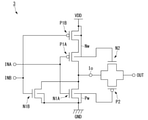
- FIG. 1 is a diagram showing an example of the configuration of a CMOS circuit (inverter circuit) according to the first embodiment.
- the inverter circuit 1 includes a P-channel MOS transistor P1, an N-channel MOS transistor N1, a P-channel MOS transistor P2, and an N-channel MOS transistor N2.
- the inverter circuit 1 shown in FIG. 1 is an example in which each transistor is formed on a P-type single crystal semiconductor substrate (bulk substrate).
- the gate terminal is connected to the input terminal IN of the inverter circuit 1, the source terminal is connected to the power supply VDD, and the drain terminal is connected to the drain terminal of the N-channel MOS transistor N1.
- the gate terminal is connected to the input terminal IN of the inverter circuit 1
- the source terminal is connected to the ground GND
- the drain terminal is connected to the drain terminal of the P-channel MOS transistor P1.
- the gate terminal is the P-well Pw of the N-channel MOS transistor N1 (the body of the N-channel MOS transistor N1 in FIG. 1)
- the source terminal is the drain of the P-channel MOS transistor P1 and the N-channel MOS transistor N1.
- the drain terminal is connected to the terminal and the drain terminal is connected to the output terminal OUT of the inverter circuit 1, respectively.
- the gate terminal is the N-well Nw of the P-channel MOS transistor P1 (the body of the P-channel MOS transistor P1 in FIG. 1)
- the source terminal is the drain of the P-channel MOS transistor P1 and the N-channel MOS transistor N1.
- the drain terminal is connected to the terminal and the drain terminal is connected to the output terminal OUT of the inverter circuit 1, respectively.
- the gate terminals of the P-channel MOS transistor P2 and the N-channel MOS transistor N2 and the corresponding wells may be connected by, for example, well contact.
- the configuration of the P-channel MOS transistor P1 and the N-channel MOS transistor N1 is the configuration of a basic logic negative circuit (inverter circuit) in a general logical operation circuit.
- the inverter circuit having a basic configuration consisting of the P-channel MOS transistor P1 and the N-channel MOS transistor N1 is referred to as a “NOT circuit” to distinguish it from the inverter circuit 1 of the first embodiment.
- the configuration of the P-channel MOS transistor P2 and the N-channel MOS transistor N2 is the configuration of a basic transmission gate circuit in a general semiconductor circuit.
- the inverter circuit 1 has a configuration including a NOT circuit having a basic configuration and a transmission gate circuit, and the node of the output terminal of the NOT circuit (hereinafter referred to as “internal node Io”) is the input terminal of the transmission gate circuit. It is connected to the.
- the P-type single crystal semiconductor substrate is an example of the "first conductive type substrate" within the scope of the claims.
- the P-channel MOS transistor P1 is an example of the "first transistor” in the claims
- the N-channel MOS transistor N1 is an example of the "second transistor” in the claims.
- N-well Nw is an example of the "first well” in the claims
- P-well Pw is an example of the "second well” in the claims.
- the P-type and P-channel are examples of the "first conductive type” in the claims
- the N-type and N-channel are examples of the "second conductive type” in the claims.
- the NOT circuit is an example of the "first logical operation circuit" in the claims.
- the P-channel MOS transistor P2 is an example of the "third transistor” in the claims, and the N-channel MOS transistor N2 is an example of the "fourth transistor” in the claims.
- the transmission gate circuit is an example of a "transmission circuit" in the claims.
- FIG. 2 is a timing chart showing an example of normal operation in the CMOS circuit (inverter circuit 1) according to the first embodiment.
- FIG. 2 is a timing chart in a normal state in which high-energy charged particles of radiation are not incident on the inverter circuit 1.
- VDD level the power supply VDD level
- GND level the ground GND level
- the input signal input to the input terminal IN is inverted at the timing delayed by a predetermined delay time in the NOT circuit, and is output to the internal node Io.
- the N-well Nw is the VDD level and the P-well Pw is the GND level. Therefore, the P-channel MOS transistor P2 and the N-channel MOS transistor N2 included in the transmission gate circuit are always on. Therefore, the signal output to the internal node Io by the NOT circuit in the normal operation of the inverter circuit 1 (hereinafter referred to as “internal signal”) is transmitted at a timing delayed by a predetermined delay time in the transmission gate circuit. It is output to the output terminal OUT.
- the internal signal output by the NOT circuit is transmitted by the transmission gate circuit and output to the output terminal OUT as an output signal. That is, in the normal operation of the inverter circuit 1, the input signal input to the input terminal IN of the inverter circuit 1 is inverted and output to the output terminal OUT, as in the general logic negative circuit.
- FIG. 3 is a diagram schematically showing an example of how high-energy charged particles are incident on the CMOS circuit (inverter circuit 1) according to the first embodiment.
- FIG. 3 shows a case where a high-energy charged particle E of radiation R is incident on a NOT circuit constituting the inverter circuit 1. Due to the incident charged particles E, a single event transient corresponding to the electric charge of the incident charged particles E is also generated in the inverter circuit 1. It is known that the incident charged particle E has a greater effect on the transistor in the off state than in the transistor in the on state.
- FIG. 4 and 5 are timing charts showing an example of operation when a single event is generated by high-energy charged particles incident on the CMOS circuit (inverter circuit 1) according to the first embodiment.
- FIG. 4 is a timing chart when a charged particle E is incident when a GND level signal is input to the input terminal IN of the inverter circuit 1
- FIG. 5 is a VDD level at the input terminal IN of the inverter circuit 1. It is a timing chart when the charged particle E is incident while the signal of is input.
- the period during which the single event transient occurred is expanded to show more detailed timing and its signal level.
- the potential level of the N well Nw decreases and the potential level of the P well Pw increases.
- the right side of FIG. 4 shows an example in which the potential level of the N-well Nw drops to the GND level and the potential level of the P-well Pw rises to a level between the VDD level and the GND level.
- the difference in the amount of change in the potential level in each well shown on the right side of FIG. 4 is that the N-well Nw is more than the P-well Pw because the semiconductor substrate forming the CMOS circuit is a P-type single crystal semiconductor substrate. Is an example of the fact that the potential level fluctuates more greatly, and it is considered that the amount of fluctuation of the potential level in each well changes according to, for example, the charge of the charged particle E.
- the transmission gate circuit does not transmit (output) the internal signal including the single event transient output to the internal node Io by the NOT circuit as it is to the output terminal OUT.
- the transmission gate circuit eliminates the transmission (output) of the single event transient included in the internal signal output to the internal node Io by the NOT circuit to the output terminal OUT.
- the transmission gate circuit reduces the single event transient included in the internal signal output to the internal node Io by the NOT circuit, and transmits (outputs) to the output terminal OUT.
- the right side of FIG. 4 shows an example in which the single event transient included in the internal signal of the internal node Io is reduced and transmitted (output) to the output terminal OUT.
- the period during which the single event transient occurred is expanded to show more detailed timing and its signal level.
- the transmission gate circuit is off from timing t3 to timing t4.
- the transmission gate circuit does not transmit (output) the internal signal including the single event transient output to the internal node Io by the NOT circuit as it is to the output terminal OUT.
- the right side of FIG. 5 shows an example in which the single event transient included in the internal signal of the internal node Io is reduced and transmitted (output) to the output terminal OUT.
- the internal signal of the internal node Io including the single event transient generated in the NOT circuit by the incident charged particles E is not output to the output terminal OUT when the transmission gate circuit is turned off.
- the single event transient output to the output terminal OUT is eliminated or reduced by the transmission gate circuit turned off by the incident charged particles E.
- the single event transient generated inside the inverter circuit 1 is not propagated to, for example, another CMOS circuit connected to the subsequent stage of the inverter circuit 1.
- the CMOS type semiconductor integrated circuit including the inverter circuit 1 it is possible to prevent the singing event upset in which erroneous data is stored due to the propagation of the signal including the generated single event transient. That is, it is possible to increase the resistance to a single event generated by the incident of the charged particles E in the CMOS circuit.
- the inverter circuit 1 has been described as an example of the CMOS circuit of the first embodiment.
- the CMOS circuit of the first embodiment may have another configuration different from that of the inverter circuit 1.
- 6 to 8 are diagrams showing another example of the configuration of the CMOS circuit according to the first embodiment.
- FIG. 6 is an example of a 2-input negative AND circuit (NAND circuit).
- the NAND circuit 2 includes a P-channel MOS transistor P1A, a P-channel MOS transistor P1B, an N-channel MOS transistor N1A, an N-channel MOS transistor N1B, a P-channel MOS transistor P2, and an N-channel MOS transistor N2.
- the NAND circuit 2 shown in FIG. 6 is an example in which each transistor is formed on a P-type single crystal semiconductor substrate.
- the configuration of the P-channel MOS transistor P1A, the P-channel MOS transistor P1B, the N-channel MOS transistor N1A, and the N-channel MOS transistor N1B is a basic negative logical product circuit (NAND circuit) in a general logical operation circuit. ).
- the configuration of the P-channel MOS transistor P2 and the N-channel MOS transistor N2 is the same as that of the transmission gate circuit in the inverter circuit 1. That is, the NAND circuit 2 includes a NAND circuit having a basic configuration and a transmission gate circuit, and the internal node Io of the output terminal of the NAND circuit is connected to the input terminal of the transmission gate circuit.
- a P-well Pw common to the N-channel MOS transistor N1A and the N-channel MOS transistor N1B is connected to the gate terminal of the P-channel MOS transistor P2, and the P-channel MOS is connected to the gate terminal of the N-channel MOS transistor N2.
- a common N-well Nw is connected between the transistor P1A and the P-channel MOS transistor P1B. Connection between the gate terminal of the P-channel MOS transistor P2 and the P-well Pw common to the N-channel MOS transistors N1A and N1B, the gate terminal of the N-channel MOS transistor N2, and the P-channel MOS transistors P1A and P-channel MOS.
- the connection with the N-well Nw common to the transistor P1B may be made by, for example, a well contact.
- the P-channel MOS transistor P1A and the P-channel MOS transistor P1B are examples of the "first transistor” in the scope of the patent claim, and the N-channel MOS transistor N1A and the N-channel MOS transistor N1B are the "second transistor” in the scope of the patent claim. Is an example.
- the basic NAND circuit is an example of the "first logical operation circuit" in the claims.
- the output signal corresponding to the input signal input to the input terminal INA and the input terminal INB of the NAND circuit 2 is output to the output terminal OUT, as in the general negative AND circuit. Will be done.
- the internal signal including the single event transient generated by any of the transistors in the off state according to the incident high-energy charged particle E is turned off by the incident charged particle E.
- the transmission gate circuit to be in the state eliminates or reduces transmission (output) to the output terminal OUT.
- FIG. 7 is an example of a 2-input NOR circuit.
- the NOR circuit 3 includes a P-channel MOS transistor P1A, a P-channel MOS transistor P1B, an N-channel MOS transistor N1A, an N-channel MOS transistor N1B, a P-channel MOS transistor P2, and an N-channel MOS transistor N2.
- the NOR circuit 3 shown in FIG. 7 is an example in which each transistor is formed on a P-type single crystal semiconductor substrate.
- the configuration of the P-channel MOS transistor P1A, the P-channel MOS transistor P1B, the N-channel MOS transistor N1A, and the N-channel MOS transistor N1B is a basic NOR circuit in a general logical operation circuit. ).
- the configuration of the P-channel MOS transistor P2 and the N-channel MOS transistor N2 is the same as that of the transmission gate circuit in the inverter circuit 1. That is, the NOR circuit 3 includes a NOR circuit having a basic configuration and a transmission gate circuit, and the internal node Io of the output terminal of the NOR circuit is connected to the input terminal of the transmission gate circuit.
- NOR circuit 3 a P-well Pw common to the N-channel MOS transistor N1A and the N-channel MOS transistor N1B is connected to the gate terminal of the P-channel MOS transistor P2, and the P-channel MOS is connected to the gate terminal of the N-channel MOS transistor N2.
- a common N-well Nw is connected between the transistor P1A and the P-channel MOS transistor P1B.
- the basic NOR circuit is an example of the "first logical operation circuit" in the claims.
- the output signal corresponding to the input signal input to the input terminal INA and the input terminal INB of the NOR circuit 3 is output to the output terminal OUT, as in the general NOR circuit. Will be done.
- the incident charged particle E turns off the internal signal including the single event transient generated by any of the transistors in the off state according to the incident high-energy charged particle E.
- the transmission gate circuit to be in the state eliminates or reduces transmission (output) to the output terminal OUT.
- FIG. 8 shows a D-type flip-flop circuit composed of six inverter circuits 1 (inverter circuits 1-1 to 1-6) and four transmission gate TMGs (transmission gates TMG-1 to TMG-4) (hereinafter, “” This is an example of "D-FF circuit”).
- the D-FF circuit 4 shown in FIG. 8 is a general D-type flip-flop circuit composed of six inverter circuits (NOT circuits) and four transmission gate TMGs, and each inverter circuit (NOT circuit) is the first. 1 It is a configuration replaced with the inverter circuit 1 of the embodiment.
- NOT circuits inverter circuits
- each inverter circuit NOT circuit
- each component included in the inverter circuits 1-1 to 1-6 is indicated by a logic gate symbol.
- the D-FF circuit 4 shown in FIG. 8 is an example in which each transistor is formed on a P-type single crystal semiconductor substrate.
- the state change of the input signal input to the input terminal D is delayed according to the clock signal CLK, and the output terminal Q While outputting to, the state of the output terminal Q is maintained. More specifically, in the D-FF circuit 4, the input signal of the input terminal D is taken in at the timing of the falling edge of the clock signal CLK, output to the output terminal Q at the timing of the rising edge of the clock signal CLK, and the clock. When the signal CLK is in another state, the output state of the output signal to the output terminal Q is maintained.
- the clock signal CLKB is an inverted clock signal of the clock signal CLK.
- each inverter circuit 1 an internal signal including a single event transient generated by one of the transistors in the off state according to the incident high-energy charged particle E is transmitted by the incident charged particle E.
- the transmission gate circuit that is turned off eliminates or reduces transmission (output) to the output terminal Q. This makes it possible to prevent a singing event upset in which erroneous data is stored in the D-FF circuit 4.
- FIG. 8 shows a D-FF circuit 4 having a configuration in which a single event upset is prevented by replacing six inverter circuits (NOT circuits) with an inverter circuit 1, but four transmissions included in the D-FF circuit 4 are shown.
- the gate TMG may also be configured by connecting a transmission gate circuit that is turned off by the incident charged particles E.
- the operation for eliminating or reducing the single event transient in each of the CMOS circuits shown in FIGS. 6 to 8 is the operation when a high-energy charged particle is incident on the inverter circuit 1 shown in FIGS. 3 to 5. It can be easily understood by thinking in the same way. Therefore, detailed description of the operation when eliminating or reducing the single event transient in each of the CMOS circuits shown in FIGS. 6 to 8 will be omitted.
- the CMOS circuit may have various configurations in addition to the respective CMOS circuits shown in FIGS. 6 to 8. These configurations are equivalent to the configurations of the inverter circuit 1 shown in FIG. 1 and the CMOS circuits (NAND circuit 2, NOR circuit 3, D-FF circuit 4) shown in FIGS.
- the CMOS circuit has a memory configuration for storing data (signal level) by combining a plurality of single logic operation circuits, flip-flop circuits, transmission gate circuits, etc., such as SRAM. Is also possible.
- the transmission gate circuit constituting this memory is a component for realizing the function of the memory. Therefore, a transmission gate circuit for eliminating or reducing single event transients may be connected to the transmission gate circuit constituting the memory.
- a transmission gate circuit that is turned off by the incident charged particles E is connected to the output terminal of the logic operation circuit having the basic configuration, and the output of the transmission gate circuit is output.
- the terminal is used as the output terminal of the CMOS circuit.
- CMOS circuit of the first embodiment it is possible to prevent a single event transient generated inside the CMOS circuit from propagating and storing erroneous data. That is, it is possible to realize a CMOS circuit having increased resistance to the incident of the charged particles E.
- the semiconductor integrated circuit having the functions realized by the CMOS circuit of the first embodiment is used in an environment where high-energy charged particles E are incident, for example, in space. It is possible to reduce the possibility of malfunction. That is, by realizing the function with the CMOS circuit of the first embodiment, it is possible to realize a highly reliable semiconductor integrated circuit with less possibility of malfunction due to the influence of the usage environment. Therefore, the semiconductor integrated circuit having the functions realized by the CMOS circuit of the first embodiment is used in an environment where high reliability is required even in places other than outer space, such as for industrial equipment, in-vehicle use, and medical use. Even when used, the effect can be obtained.
- the transmission gate circuit is formed by connecting wells of transistors having different conductive types included in the logic operation circuit having a basic configuration to the gate terminal of each transistor included in the transmission gate circuit.
- the configuration which is turned off by the incident charged particle E is shown.
- the configuration in which the transmission gate circuit is turned off by the incident charged particles E may be another configuration.
- CMOS circuit of the second embodiment will be described. Also in the following description, in order to facilitate the explanation, a logic negation circuit (inverter circuit), which is a logic operation circuit having the simplest configuration, will be described as an example of the CMOS circuit of the second embodiment.
- inverter circuit which is a logic operation circuit having the simplest configuration
- FIG. 9 is a diagram showing an example of the configuration of the CMOS circuit (inverter circuit) according to the second embodiment.
- the inverter circuit 1A includes a P-channel MOS transistor P1, an N-channel MOS transistor N1, a P-channel MOS transistor P2, an N-channel MOS transistor N2, a P-channel MOS transistor P3, an N-channel MOS transistor N3, and a P-channel MOS.
- a transistor P4 and an N-channel MOS transistor N4 are provided.
- the inverter circuit 1A shown in FIG. 9 is an example in which each transistor is formed on a P-type single crystal semiconductor substrate.
- the configuration of the P-channel MOS transistor P1 and the N-channel MOS transistor N1 is connected to the input terminal IN, similarly to the NOT circuit included in the inverter circuit 1 of the first embodiment.
- the internal node Io of the output terminal of the NOT circuit is connected to the input terminal of the transmission gate circuit composed of the P-channel MOS transistor P2 and the N-channel MOS transistor N2.
- a ground GND is connected to the input terminal of a NOT circuit (hereinafter referred to as "NOT circuit A”) composed of a P-channel MOS transistor P3 and an N-channel MOS transistor N3, and an output terminal is an N constituting a transmission gate circuit. It is connected to the gate terminal of the channel MOS transistor N2.
- a power supply VDD is connected to an input terminal of a NOT circuit (hereinafter referred to as "NOT circuit B") composed of a P-channel MOS transistor P4 and an N-channel MOS transistor N4, and an output terminal is a P constituting a transmission gate circuit. It is connected to the gate terminal of the channel MOS transistor P2.
- the wells of the P-channel MOS transistor P1, the P-channel MOS transistor P3, and the P-channel MOS transistor P4 are common N-wells Nw.
- the wells of the N-channel MOS transistor N1, the N-channel MOS transistor N3, and the N-channel MOS transistor N4 are common P-wells Pw.
- the connection between the gate terminal of the N-channel MOS transistor N2 and the output terminal of the NOT circuit A and the connection between the gate terminal of the P-channel MOS transistor P2 and the output terminal of the NOT circuit B are, for example, a manufacturing process of a CMOS type semiconductor integrated circuit. It may be performed in the wiring process in.
- the output terminal of the transmission gate circuit composed of the P-channel MOS transistor P2 and the N-channel MOS transistor N2 is connected to the output terminal OUT, similarly to the transmission gate circuit included in the inverter circuit 1 of the first embodiment.
- the P-channel MOS transistor P3 is an example of the "fifth transistor” in the claims, and the N-channel MOS transistor N3 is an example of the "sixth transistor” in the claims.
- the NOT circuit A is an example of the "second logical operation circuit” in the claims.
- the P-channel MOS transistor P4 is an example of the "seventh transistor” in the claims, and the N-channel MOS transistor N4 is an example of the "eighth transistor” in the claims.
- the NOT circuit B is an example of the "second logical operation circuit” in the claims.
- the input terminal of the NOT circuit A is fixed to the ground GND, so that "High” level (for example, VDD level) is always output, and the input terminal of the NOT circuit B is fixed to the power supply VDD. Therefore, the "Low” level (for example, GND level) is always output. Therefore, the P-channel MOS transistor P2 and the N-channel MOS transistor N2 included in the transmission gate circuit are always on. Therefore, in the normal operation of the inverter circuit 1A, the internal signal output to the internal node Io by the NOT circuit is transmitted at a timing delayed by a predetermined delay time in the transmission gate circuit and output to the output terminal OUT. ..
- the inverter circuit 1A when a high-energy charged particle E is incident, a single event transient is generated according to the charge of the incident charged particle E in any of the transistors in the off state provided in the inverter circuit 1A. Therefore, also in the inverter circuit 1A, the potential level of the N-well Nw common to the P-channel MOS transistor is lowered for the same reason as described in the first embodiment, and the P-well Pw common to the N-channel MOS transistor is reduced. The potential level goes up. As a result, in the inverter circuit 1A, the NOT circuit A outputs the “Low” level, and the NOT circuit B outputs the “High” level.
- the transmission gate circuit is turned off according to the incident high-energy charged particles E, as in the case of the inverter circuit 1 of the first embodiment.
- an internal signal including a single event transient generated by any of the transistors in the off state according to the incident high-energy charged particles E is transmitted.
- the transmission gate circuit turned off by the incident charged particles E eliminates or reduces transmission (output) to the output terminal OUT.
- FIG. 10 is a diagram showing another example of the configuration of the CMOS circuit (inverter circuit) according to the second embodiment.
- the inverter circuit 1B includes a P-channel MOS transistor P1, an N-channel MOS transistor N1, an N-channel MOS transistor N2, a P-channel MOS transistor P3, and an N-channel MOS transistor N3.
- the inverter circuit 1B shown in FIG. 10 is an example in which each transistor is formed on a P-type single crystal semiconductor substrate.
- the transmission gate circuit included in the inverter circuit 1A is composed of only the N-channel MOS transistor N2, and the NOT circuit B is deleted accordingly. Therefore, the inverter circuit 1B can form a CMOS circuit with a circuit scale smaller than that of the inverter circuit 1A.
- the inverter circuit 1B has a different transmission gate circuit configuration, but its operation is the same as that of the inverter circuit 1A. Therefore, in the inverter circuit 1B as well, as in the inverter circuit 1 and the inverter circuit 1A, an internal signal including a single event transient generated by any of the transistors in the off state according to the incident high-energy charged particle E is incident.
- the transmission gate circuit turned off by the charged particles E eliminates or reduces transmission (output) to the output terminal OUT.
- the well is turned off by the output signal of the NOT circuit A and / or the NOT circuit B in which the well is composed of a common transistor at the output terminal of the logic arithmetic circuit of the basic configuration.
- the transmission gate circuit to be in the state is connected, and the output terminal of the transmission gate circuit is used as the output terminal of the CMOS circuit.
- the operation of the transmission gate circuit in the CMOS circuit of the second embodiment to the off state can be considered to be an operation due to indirectly detecting the fluctuation of the potential level of the well.
- the well is directly connected to the gate terminal of each transistor included in the transmission gate circuit, so that the fluctuation of the potential level of the well is directly detected and the transmission gate is transmitted.
- the circuit is turned off, whereas in the CMOS circuit of the second embodiment, the transmission gate circuit is turned off due to the change in the potential level of the output signal of the NOT circuit A and / or the NOT circuit B having a common well. Because it becomes.
- the transmission gate circuit has the fluctuation of the potential level of the well due to the incident high-energy charged particles E. Is detected and turned off.
- the internal including the single event transient generated by any of the transistors in the off state according to the charged particle E incident on the CMOS circuit. Eliminates or reduces the signal being transmitted (output) to the output terminal OUT.
- the single event transient generated inside the CMOS circuit is connected to, for example, another CMOS circuit after the CMOS circuit. It is possible to prevent the single event transient from being propagated to the CMOS, and it is possible to prevent the single event transient from being propagated and the singing event upset in which erroneous data is stored. That is, the CMOS circuit of the second embodiment can also increase the resistance to the incident of the charged particles E as in the CMOS circuit of the first embodiment. As a result, even in the CMOS circuit of the second embodiment, it is possible to realize a highly reliable semiconductor integrated circuit with less possibility of malfunction due to the influence of the usage environment.
- the CMOS circuit of each embodiment even if a single event transient is generated in the logical operation circuit due to the incident of high energy charged particles of radiation from the usage environment, the generated single event transient is generated. It can be eliminated or reduced from being transmitted (output) to the output terminal OUT. As a result, the semiconductor integrated circuit having the functions realized by the CMOS circuit of each embodiment reduces the possibility of malfunction even when used in an environment where high-energy charged particles are incident. And high reliability can be obtained.
- the semiconductor substrate includes various structures such as an N-type single crystal substrate and a P-type or N-type SOI structure substrate in addition to the P-type single crystal substrate.
- the configuration and operation of the CMOS circuit may be equivalent to the configuration and operation of the CMOS circuit formed on the P-type single crystal semiconductor substrate described above. Therefore, detailed description of the configuration and operation when the CMOS circuit is formed on a semiconductor substrate different from the P-type single crystal semiconductor substrate will be omitted.
Landscapes
- Engineering & Computer Science (AREA)
- Power Engineering (AREA)
- Physics & Mathematics (AREA)
- Computer Hardware Design (AREA)
- Computing Systems (AREA)
- General Engineering & Computer Science (AREA)
- Mathematical Physics (AREA)
- Metal-Oxide And Bipolar Metal-Oxide Semiconductor Integrated Circuits (AREA)
- Logic Circuits (AREA)
Abstract
第一導電型の基板に形成されるCMOS回路であって、第1論理演算回路は、第一導電型と異なる第二導電型の第1ウェルを有する第一導電型の第1トランジスタと、第一導電型の第2ウェルを有する第二導電型の第2トランジスタとの組み合わせを備え、伝送回路は、第1論理演算回路の出力端子に接続され、第一導電型の第3トランジスタと、第二導電型の第4トランジスタとのいずれか一方または両方を備え、第3トランジスタと第4トランジスタとのゲート端子には、第1トランジスタおよび第2トランジスタのうち導電型が異なるトランジスタのウェル、あるいは、第1ウェルを有する第一導電型の第5トランジスタと、第2ウェルを有する第二導電型の第6トランジスタとの組み合わせを備え、入力端子が所定の電位に固定された第2論理演算回路の出力端子が接続される。
Description
本発明は、CMOS回路に関する。
本願は、2020年08月07日に出願された日本国特許出願2020-134718号に基づき優先権を主張し、その内容をここに援用する。
本願は、2020年08月07日に出願された日本国特許出願2020-134718号に基づき優先権を主張し、その内容をここに援用する。
従来から、例えば、CMOS(Complementary Metal Oxide Semiconductor:相補型金属酸化膜半導体)型のLSI(Large Scale Integration)やASIC(Application Specific Integrated Circuit)、FPGA(Field-Programmable Gate Array)、GPU(Graphics Processing Unit)などの半導体集積回路が、様々な機器や装置に使用されている。CMOS型半導体集積回路では、半導体基板(例えば、シリコン基板)上に形成されたトランジスタなどの回路素子を複数繋げて回路を形成することにより、必要な動作をする機能が実現される。
例えば、地球を周回する人工衛星など、宇宙空間において使用されるCMOS型半導体集積回路は、例えば、高エネルギーの荷電粒子などの放射線が入射してしまう環境で使用される。さらに、地上で使用されるCMOS型半導体集積回路も、例えば、中性子などの放射線の影響を受けることが知られている。CMOS型半導体集積回路に入射した放射線は、半導体基板上に形成された回路素子が誤動作してしまう要因となることが知られている。より具体的には、CMOS型半導体集積回路に高エネルギーの荷電粒子が入射すると、例えば、電位の変動(いわゆる、シングルイベントトランジェント:Single Event Transient:SET)や、電位の変動の影響を受けた信号の伝搬による誤ったデータの記憶(いわゆる、シングイベントアップセット:Single Event Upset:SEU)などが発生することが知られている。
従来から、シングルイベントトランジェントやシングイベントアップセットなどのシングルイベントに対する対策をするための種々の技術が開示されている(特許文献1、非特許文献1参照)。例えば、特許文献1には、回路素子を二重化構造(縦積みの構造)にすることにより、高エネルギーの荷電粒子によって発生したシングルイベントによる誤動作を後段に伝搬させないようにすることが開示されている。例えば、非特許文献1には、シングルイベントのエラー(ソフトエラー)に対する耐性(ロバスト性)を高めた組み込み型の回路素子の設計(構造)に関する技術が開示されている。
S.Mitra、N.Seifert、M.Zhang、Q.Shi、K.S.Kim、"Robust system design with built-in soft-error resilience"、IEEE Computer Society、vol.38、no.2、pp.43-52、Feb.2005、doi:10.1109/MC.2005.70.
しかしながら、特許文献1に開示された技術は、SOI(Silicon on Insulator)構造の半導体基板に回路素子を形成する場合にのみ有効な技術である。SOI構造の半導体基板は、基板の内部に絶縁体の層を設けている構造となっているため、例えば、シリコンの単結晶の基板(いわゆる、バルク基板)に比べて高価なものである。さらに、近年では、CMOS型半導体集積回路の製造プロセスの微細化が進んできている。このため、従来の技術を適用した回路素子は、製造プロセスの微細化に伴って、シングルイベントへの対策効果を期待することができなくなってきている。これは、従来の技術では、回路素子を構成するそれぞれの構成要素の間に空間的な距離を設けることによってシングルイベントへの対策を行っているが、製造プロセスが微細化すると半導体基板上に形成される回路素子が小さくなり、それぞれの構成要素の間に必要な距離を確保することができなくなってしまい、従来の技術によるシングルイベントへの対策効果が無効化されてしまうからである。
本発明は、上記の課題認識に基づいてなされたものであり、シングルイベントに対する耐性が高いCMOS回路を提供することを目的としている。
上記目的を達成するため、本発明の一態様に係るCMOS回路は、第一導電型の基板に形成された第1論理演算回路、および前記第1論理演算回路の出力端子の信号を伝送する伝送回路を備えるCMOS回路であって、前記第1論理演算回路は、前記第一導電型と異なる第二導電型の第1ウェルを有する前記第一導電型の第1トランジスタと、前記第一導電型の第2ウェルを有する前記第二導電型の第2トランジスタと、の組み合わせを備え、前記伝送回路は、前記第1論理演算回路の出力端子に接続され、前記第一導電型の第3トランジスタと、前記第二導電型の第4トランジスタとのいずれか一方または両方を備え、前記第3トランジスタと前記第4トランジスタとのゲート端子には、前記第1トランジスタおよび前記第2トランジスタのうち導電型が異なるトランジスタのウェル、あるいは、前記第1ウェルを有する前記第一導電型の第5トランジスタと、前記第2ウェルを有する前記第二導電型の第6トランジスタと、の組み合わせを備え、入力端子が所定の電位に固定された第2論理演算回路の出力端子が接続される、CMOS回路である。
本発明の一態様によれば、CMOS回路におけるシングルイベントへの耐性を高くすることができる。
以下、図面を参照し、本発明のCMOS(Complementary Metal Oxide Semiconductor:相補型金属酸化膜半導体)回路の実施形態について説明する。本出願が日本語から英語に翻訳された場合、本開示全体を通して使用されるように、単数形「a」、「an」、および「the」は、文脈が明らかにそうでないことを示していない限り、複数形のリファレンスを含むとみなしてよい。実施形態のCMOS回路は、例えば、論理否定回路(NOT回路あるいはインバータ回路)、論理和回路(OR回路)、論理積回路(AND回路)、否定論理和回路(NOR回路)、否定論理積回路(NAND回路)、排他的論理和回路(EXOR回路)、否定排他的論理和回路(EXNOR回路)など、論理演算を行う単独の論理演算回路である。実施形態のCMOS回路は、単独の論理演算回路を複数組み合わせることによって、例えば、ラッチ回路やフリップフロップ回路など、データ(信号レベル)を保持する構成にすることもできる。さらに、実施形態のCMOS回路は、単独の論理演算回路や、フリップフロップ回路、伝送ゲート回路などを複数組み合わせることによって、例えば、SRAM(Static Random Access Memory)など、データ(信号レベル)を記憶する(メモリする)構成にすることもできる。
<第1実施形態>
以下の説明においては、説明を容易にするため、最も簡単な構成の論理演算回路である論理否定回路(以下、「インバータ回路」という)を、第1実施形態のCMOS回路の一例として説明する。
以下の説明においては、説明を容易にするため、最も簡単な構成の論理演算回路である論理否定回路(以下、「インバータ回路」という)を、第1実施形態のCMOS回路の一例として説明する。
[インバータ回路の構成]
図1は、第1実施形態に係るCMOS回路(インバータ回路)の構成の一例を示す図である。インバータ回路1は、PチャンネルMOSトランジスタP1と、NチャンネルMOSトランジスタN1と、PチャンネルMOSトランジスタP2と、NチャンネルMOSトランジスタN2と、を備える。図1に示したインバータ回路1は、P型の単結晶の半導体基板(バルク基板)にそれぞれのトランジスタを形成した場合の一例である。
図1は、第1実施形態に係るCMOS回路(インバータ回路)の構成の一例を示す図である。インバータ回路1は、PチャンネルMOSトランジスタP1と、NチャンネルMOSトランジスタN1と、PチャンネルMOSトランジスタP2と、NチャンネルMOSトランジスタN2と、を備える。図1に示したインバータ回路1は、P型の単結晶の半導体基板(バルク基板)にそれぞれのトランジスタを形成した場合の一例である。
PチャンネルMOSトランジスタP1は、ゲート端子がインバータ回路1の入力端子INに、ソース端子が電源VDDに、ドレイン端子がNチャンネルMOSトランジスタN1のドレイン端子に、それぞれ接続されている。NチャンネルMOSトランジスタN1は、ゲート端子がインバータ回路1の入力端子INに、ソース端子がグラウンドGNDに、ドレイン端子がPチャンネルMOSトランジスタP1のドレイン端子に、それぞれ接続されている。PチャンネルMOSトランジスタP2は、ゲート端子がNチャンネルMOSトランジスタN1のPウェルPw(図1では、NチャンネルMOSトランジスタN1のボディ)に、ソース端子がPチャンネルMOSトランジスタP1およびNチャンネルMOSトランジスタN1のドレイン端子に、ドレイン端子がインバータ回路1の出力端子OUTに、それぞれ接続されている。NチャンネルMOSトランジスタN2は、ゲート端子がPチャンネルMOSトランジスタP1のNウェルNw(図1では、PチャンネルMOSトランジスタP1のボディ)に、ソース端子がPチャンネルMOSトランジスタP1およびNチャンネルMOSトランジスタN1のドレイン端子に、ドレイン端子がインバータ回路1の出力端子OUTに、それぞれ接続されている。PチャンネルMOSトランジスタP2およびNチャンネルMOSトランジスタN2のゲート端子と、対応するウェルは、例えば、ウェルコンタクトなどによって接続されてもよい。
インバータ回路1において、PチャンネルMOSトランジスタP1とNチャンネルMOSトランジスタN1との構成は、一般的な論理演算回路における基本的な論理否定回路(インバータ回路)の構成である。以下の説明においては、PチャンネルMOSトランジスタP1とNチャンネルMOSトランジスタN1とによる基本的な構成のインバータ回路を、「NOT回路」といって、第1実施形態のインバータ回路1と区別する。インバータ回路1において、PチャンネルMOSトランジスタP2とNチャンネルMOSトランジスタN2との構成は、一般的な半導体回路における基本的な伝送ゲート回路の構成である。つまり、インバータ回路1は、基本的な構成のNOT回路と伝送ゲート回路とを備える構成であり、NOT回路の出力端子のノード(以下、「内部ノードIo」という)が、伝送ゲート回路の入力端子に接続されている。
P型の単結晶の半導体基板は、特許請求の範囲における「第一導電型の基板」の一例である。PチャンネルMOSトランジスタP1は、特許請求の範囲における「第1トランジスタ」の一例であり、NチャンネルMOSトランジスタN1は、特許請求の範囲における「第2トランジスタ」の一例である。NウェルNwは、特許請求の範囲における「第1ウェル」の一例であり、PウェルPwは、特許請求の範囲における「第2ウェル」の一例である。P型やPチャンネルは、特許請求の範囲における「第一導電型」の一例であり、N型やNチャンネルは、特許請求の範囲における「第二導電型」の一例である。NOT回路は、特許請求の範囲における「第1論理演算回路」の一例である。PチャンネルMOSトランジスタP2は、特許請求の範囲における「第3トランジスタ」の一例であり、NチャンネルMOSトランジスタN2は、特許請求の範囲における「第4トランジスタ」の一例である。伝送ゲート回路は、特許請求の範囲における「伝送回路」の一例である。
[インバータ回路の動作]
以下、インバータ回路1の動作タイミングについて説明する。まず、インバータ回路1における通常の動作について説明する。図2は、第1実施形態に係るCMOS回路(インバータ回路1)における通常の動作の一例を示すタイミングチャートである。図2は、インバータ回路1に放射線の高エネルギーの荷電粒子が入射していない通常の状態のタイミングチャートである。以下の説明においては、インバータ回路1におけるそれぞれの信号の“High”レベルを電源VDDのレベル(以下、「VDDレベル」という)とし、“Low”レベルをグラウンドGNDのレベル(以下、「GNDレベル」という)とする。
以下、インバータ回路1の動作タイミングについて説明する。まず、インバータ回路1における通常の動作について説明する。図2は、第1実施形態に係るCMOS回路(インバータ回路1)における通常の動作の一例を示すタイミングチャートである。図2は、インバータ回路1に放射線の高エネルギーの荷電粒子が入射していない通常の状態のタイミングチャートである。以下の説明においては、インバータ回路1におけるそれぞれの信号の“High”レベルを電源VDDのレベル(以下、「VDDレベル」という)とし、“Low”レベルをグラウンドGNDのレベル(以下、「GNDレベル」という)とする。
図2には、所定の時間間隔でVDDレベルとGNDレベルとの間で信号レベルが変化させて入力信号がインバータ回路1の入力端子INに入力された場合において、入力端子IN、内部ノードIo、出力端子OUT、NウェルNw、およびPウェルPwのそれぞれの信号が変化するタイミングとその信号レベルとを示している。
インバータ回路1の通常の動作では、入力端子INに入力された入力信号が、NOT回路における所定の遅延時間だけ遅延したタイミングで反転されて、内部ノードIoに出力される。インバータ回路1において、NウェルNwはVDDレベルであり、PウェルPwはGNDレベルである。従って、伝送ゲート回路が備えるPチャンネルMOSトランジスタP2とNチャンネルMOSトランジスタN2とは、常にオン状態である。このため、インバータ回路1の通常の動作においてNOT回路により内部ノードIoに出力された信号(以下、「内部信号」という)は、伝送ゲート回路における所定の遅延時間だけ遅延したタイミングで伝送されて、出力端子OUTに出力される。
このように、インバータ回路1の通常の動作では、NOT回路により出力された内部信号が伝送ゲート回路によって伝送され、出力信号として出力端子OUTに出力される。つまり、インバータ回路1における通常の動作では、一般的な論理否定回路と同様に、インバータ回路1の入力端子INに入力された入力信号が反転されて、出力端子OUTに出力される。
次に、インバータ回路1に放射線の高エネルギーの荷電粒子が入射した場合の動作について説明する。図3は、第1実施形態に係るCMOS回路(インバータ回路1)に高エネルギーの荷電粒子が入射する様子の一例を模式的に示す図である。図3には、放射線Rの高エネルギーの荷電粒子Eが、インバータ回路1を構成するNOT回路に入射した場合を示している。入射した荷電粒子Eにより、インバータ回路1においても、入射した荷電粒子Eの電荷に応じたシングルイベントトランジェントが発生する。入射した荷電粒子Eは、オン状態のトランジスタよりも、オフ状態のトランジスタに対してより大きな影響を与えることが知られている。
図4および図5は、第1実施形態に係るCMOS回路(インバータ回路1)に入射した高エネルギーの荷電粒子によりシングルイベントが発生した場合の動作の一例を示すタイミングチャートである。図4は、インバータ回路1の入力端子INにGNDレベルの信号が入力されているときに荷電粒子Eが入射した場合のタイミングチャートであり、図5は、インバータ回路1の入力端子INにVDDレベルの信号が入力されているときに荷電粒子Eが入射した場合のタイミングチャートである。
まず、図4に示したタイミングチャートについて説明する。インバータ回路1の入力端子INにGNDレベルの信号が入力されているタイミングt1のときにNOT回路に荷電粒子Eが入射すると、入射した荷電粒子Eの電荷に応じて、NOT回路を構成するオフ状態であるNチャンネルMOSトランジスタN1の電位が過渡的に変動する。これにより、NOT回路の出力信号である内部ノードIoにGNDレベルの瞬時的なパルスが表れる。これが、シングルイベントトランジェントである。
図4の右側には、シングルイベントトランジェントが発生した期間を拡大して、より詳細なタイミングとその信号レベルとを示している。シングルイベントトランジェントの発生に伴って、例えば、NウェルNwの電位レベルが下がり、PウェルPwの電位レベルが上がる。図4の右側には、NウェルNwの電位レベルがGNDレベルまで下がり、PウェルPwの電位レベルがVDDレベルとGNDレベルとの間のレベルまで上がった場合の一例を示している。図4の右側に示したそれぞれのウェルにおける電位レベルの変動量の違いは、CMOS回路を形成する半導体基板がP型の単結晶の半導体基板であるため、PウェルPwよりもNウェルNwの方がより大きく電位レベルが変動すると考えたことによる一例であり、それぞれのウェルにおける電位レベルの変動量は、例えば、荷電粒子Eの電荷に応じて変わるものと考えられる。
すると、NウェルNwの電位レベルが下がったことにより、伝送ゲート回路を構成するNチャンネルMOSトランジスタN2がオフ状態になり、PウェルPwの電位レベルが上がったことにより、伝送ゲート回路を構成するPチャンネルMOSトランジスタP2がオフ状態になる。つまり、伝送ゲート回路は、オフ状態になる。図4の右側では、タイミングt1からタイミングt2までの間、伝送ゲート回路がオフ状態である。これにより、伝送ゲート回路は、NOT回路により内部ノードIoに出力されたシングルイベントトランジェントを含む内部信号を、そのまま出力端子OUTに伝送(出力)しなくなる。言い換えれば、伝送ゲート回路は、NOT回路により内部ノードIoに出力された内部信号に含まれるシングルイベントトランジェントの出力端子OUTへの伝送(出力)を排除する。あるいは、伝送ゲート回路は、NOT回路により内部ノードIoに出力された内部信号に含まれるシングルイベントトランジェントを低減させて、出力端子OUTに伝送(出力)する。図4の右側には、内部ノードIoの内部信号に含まれるシングルイベントトランジェントが低減されて出力端子OUTに伝送(出力)されている場合の一例を示している。
次に、図5に示したタイミングチャートについて説明する。インバータ回路1の入力端子INにVDDレベルの信号が入力されているタイミングt3のときにNOT回路に荷電粒子Eが入射すると、入射した荷電粒子Eの電荷に応じて、NOT回路を構成するオフ状態であるPチャンネルMOSトランジスタP1の電位が変動する。これにより、NOT回路の出力信号である内部ノードIoにVDDレベルの瞬時的なパルスが表れる。
図5の右側には、シングルイベントトランジェントが発生した期間を拡大して、より詳細なタイミングとその信号レベルとを示している。シングルイベントトランジェントの発生に伴って、図4に示したインバータ回路1の入力端子INにGNDレベルの信号が入力されているときにNOT回路に荷電粒子Eが入射した場合と同様に、伝送ゲート回路は、オフ状態になる。図5の右側では、タイミングt3からタイミングt4までの間、伝送ゲート回路がオフ状態である。これにより、伝送ゲート回路は、NOT回路により内部ノードIoに出力されたシングルイベントトランジェントを含む内部信号を、そのまま出力端子OUTに伝送(出力)しなくなる。図5の右側には、内部ノードIoの内部信号に含まれるシングルイベントトランジェントが低減されて出力端子OUTに伝送(出力)されている場合の一例を示している。
このように、インバータ回路1では、入射した荷電粒子EによってNOT回路で発生したシングルイベントトランジェントを含む内部ノードIoの内部信号を、伝送ゲート回路がオフ状態になることによって出力端子OUTに出力しないようにする。言い換えれば、インバータ回路1では、入射した荷電粒子Eによってオフ状態にされる伝送ゲート回路によって、出力端子OUTに出力されるシングルイベントトランジェントを排除または低減させる。これにより、インバータ回路1では、インバータ回路1の内部で発生したシングルイベントトランジェントを、例えば、インバータ回路1の後段に接続されている他のCMOS回路に伝搬させることがなくなる。このことにより、インバータ回路1を備えるCMOS型半導体集積回路では、発生したシングルイベントトランジェントを含む信号の伝搬によって誤ったデータが記憶されてしまうシングイベントアップセットを防止することができる。つまり、CMOS回路に荷電粒子Eが入射したことによって発生するシングルイベントに対する耐性を高くすることができる。
[他のCMOS回路の構成]
以上の説明では、第1実施形態のCMOS回路の一例として、インバータ回路1について説明した。しかし、第1実施形態のCMOS回路は、インバータ回路1と異なる他の構成も考えられる。以下、第1実施形態のCMOS回路におけるインバータ回路1以外の他のCMOS回路の構成の一例について説明する。図6~図8は、第1実施形態に係るCMOS回路の構成の別の一例を示す図である。
以上の説明では、第1実施形態のCMOS回路の一例として、インバータ回路1について説明した。しかし、第1実施形態のCMOS回路は、インバータ回路1と異なる他の構成も考えられる。以下、第1実施形態のCMOS回路におけるインバータ回路1以外の他のCMOS回路の構成の一例について説明する。図6~図8は、第1実施形態に係るCMOS回路の構成の別の一例を示す図である。
図6は、2入力の否定論理積回路(NAND回路)の一例である。NAND回路2は、PチャンネルMOSトランジスタP1Aと、PチャンネルMOSトランジスタP1Bと、NチャンネルMOSトランジスタN1Aと、NチャンネルMOSトランジスタN1Bと、PチャンネルMOSトランジスタP2と、NチャンネルMOSトランジスタN2と、を備える。図6に示したNAND回路2は、P型の単結晶の半導体基板にそれぞれのトランジスタを形成した場合の一例である。
NAND回路2において、PチャンネルMOSトランジスタP1A、PチャンネルMOSトランジスタP1B、NチャンネルMOSトランジスタN1A、およびNチャンネルMOSトランジスタN1Bの構成は、一般的な論理演算回路における基本的な否定論理積回路(NAND回路)の構成である。NAND回路2において、PチャンネルMOSトランジスタP2とNチャンネルMOSトランジスタN2との構成は、インバータ回路1における伝送ゲート回路と同様である。つまり、NAND回路2は、基本的な構成のNAND回路と伝送ゲート回路とを備え、NAND回路の出力端子の内部ノードIoが、伝送ゲート回路の入力端子に接続されている。NAND回路2では、PチャンネルMOSトランジスタP2のゲート端子に、NチャンネルMOSトランジスタN1AとNチャンネルMOSトランジスタN1Bとで共通のPウェルPwが接続され、NチャンネルMOSトランジスタN2のゲート端子に、PチャンネルMOSトランジスタP1AとPチャンネルMOSトランジスタP1Bとで共通のNウェルNwが接続されている。PチャンネルMOSトランジスタP2のゲート端子と、NチャンネルMOSトランジスタN1AおよびNチャンネルMOSトランジスタN1Bで共通のPウェルPwとの接続、NチャンネルMOSトランジスタN2のゲート端子と、PチャンネルMOSトランジスタP1AおよびPチャンネルMOSトランジスタP1Bで共通のNウェルNwとの接続は、例えば、ウェルコンタクトなどによって行われてもよい。
PチャンネルMOSトランジスタP1AおよびPチャンネルMOSトランジスタP1Bは、特許請求の範囲における「第1トランジスタ」の一例であり、NチャンネルMOSトランジスタN1AおよびNチャンネルMOSトランジスタN1Bは、特許請求の範囲における「第2トランジスタ」の一例である。基本的なNAND回路は、特許請求の範囲における「第1論理演算回路」の一例である。
NAND回路2においても、通常の動作では、一般的な否定論理積回路と同様に、NAND回路2の入力端子INAおよび入力端子INBに入力された入力信号に応じた出力信号が出力端子OUTに出力される。NAND回路2においても、インバータ回路1と同様に、入射した高エネルギーの荷電粒子Eに応じてオフ状態のいずれかのトランジスタで発生したシングルイベントトランジェントを含む内部信号を、入射した荷電粒子Eによってオフ状態にされる伝送ゲート回路によって、出力端子OUTに伝送(出力)されるのを排除または低減させる。
図7は、2入力の否定論理和回路(NOR回路)の一例である。NOR回路3は、PチャンネルMOSトランジスタP1Aと、PチャンネルMOSトランジスタP1Bと、NチャンネルMOSトランジスタN1Aと、NチャンネルMOSトランジスタN1Bと、PチャンネルMOSトランジスタP2と、NチャンネルMOSトランジスタN2と、を備える。図7に示したNOR回路3は、P型の単結晶の半導体基板にそれぞれのトランジスタを形成した場合の一例である。
NOR回路3において、PチャンネルMOSトランジスタP1A、PチャンネルMOSトランジスタP1B、NチャンネルMOSトランジスタN1A、およびNチャンネルMOSトランジスタN1Bの構成は、一般的な論理演算回路における基本的な否定論理和回路(NOR回路)の構成である。NOR回路3において、PチャンネルMOSトランジスタP2とNチャンネルMOSトランジスタN2との構成は、インバータ回路1における伝送ゲート回路と同様である。つまり、NOR回路3は、基本的な構成のNOR回路と伝送ゲート回路とを備え、NOR回路の出力端子の内部ノードIoが、伝送ゲート回路の入力端子に接続されている。NOR回路3では、PチャンネルMOSトランジスタP2のゲート端子に、NチャンネルMOSトランジスタN1AとNチャンネルMOSトランジスタN1Bとで共通のPウェルPwが接続され、NチャンネルMOSトランジスタN2のゲート端子に、PチャンネルMOSトランジスタP1AとPチャンネルMOSトランジスタP1Bとで共通のNウェルNwが接続されている。
基本的なNOR回路は、特許請求の範囲における「第1論理演算回路」の一例である。
NOR回路3においても、通常の動作では、一般的な否定論理和回路と同様に、NOR回路3の入力端子INAおよび入力端子INBに入力された入力信号に応じた出力信号が出力端子OUTに出力される。NOR回路3においても、インバータ回路1と同様に、入射した高エネルギーの荷電粒子Eに応じてオフ状態のいずれかのトランジスタで発生したシングルイベントトランジェントを含む内部信号を、入射した荷電粒子Eによってオフ状態にされる伝送ゲート回路によって、出力端子OUTに伝送(出力)されるのを排除または低減させる。
図8は、六つのインバータ回路1(インバータ回路1-1~1-6)と四つのトランスミッションゲートTMG(トランスミッションゲートTMG-1~TMG-4)とで構成したD型フリップフロップ回路(以下、「D-FF回路」という)の一例である。図8に示したD-FF回路4は、六つのインバータ回路(NOT回路)と四つのトランスミッションゲートTMGとで構成した一般的なD型フリップフロップ回路において、それぞれのインバータ回路(NOT回路)を第1実施形態のインバータ回路1に置き換えた構成である。図8においては、インバータ回路1-1~1-6が備えるそれぞれの構成要素を論理ゲート記号で示している。図8に示したD-FF回路4は、P型の単結晶の半導体基板にそれぞれのトランジスタを形成した場合の一例である。
D-FF回路4においても、通常の動作では、一般的なD型フリップフロップ回路と同様に、入力端子Dに入力された入力信号の状態変化をクロック信号CLKに応じて遅延させて出力端子Qに出力するとともに、出力端子Qの状態を保持する。より具体的には、D-FF回路4では、入力端子Dの入力信号をクロック信号CLKの立ち下がりエッジのタイミングで取り込み、クロック信号CLKの立ち上がりエッジのタイミングで出力端子Qに出力するとともに、クロック信号CLKが他の状態のときには、出力信号の出力端子Qへの出力状態を保持する。図8においてクロック信号CLKBは、クロック信号CLKの反転クロック信号である。D-FF回路4では、それぞれのインバータ回路1において、入射した高エネルギーの荷電粒子Eに応じてオフ状態のいずれかのトランジスタで発生したシングルイベントトランジェントを含む内部信号を、入射した荷電粒子Eによってオフ状態にされる伝送ゲート回路によって、出力端子Qに伝送(出力)されるのを排除または低減させる。これにより、D-FF回路4において誤ったデータが記憶されてしまうシングイベントアップセットを防止することができる。図8においては、六つのインバータ回路(NOT回路)をインバータ回路1に置き換えることによってシングイベントアップセットを防止する構成のD-FF回路4を示したが、D-FF回路4が備える四つのトランスミッションゲートTMGも、入射した荷電粒子Eによってオフ状態にされる伝送ゲート回路を接続した構成にしてもよい。
図6~図8に示したそれぞれのCMOS回路においてシングルイベントトランジェントを排除または低減させる際の動作は、図3~図5に示したインバータ回路1に高エネルギーの荷電粒子が入射した場合の動作と同様に考えることによって、容易に理解することができる。従って、図6~図8に示したそれぞれのCMOS回路においてシングルイベントトランジェントを排除または低減させる際の動作に関する詳細な説明は省略する。さらに、上述したように、CMOS回路は、図6~図8に示したそれぞれのCMOS回路の他にも種々の構成が考えられる。これらの構成は、図1に示したインバータ回路1や、図6~図8に示したCMOS回路(NAND回路2、NOR回路3、D-FF回路4)の構成と等価なものになるように構成すればよい。さらに、上述したように、CMOS回路は、例えば、SRAMなどのように、単独の論理演算回路や、フリップフロップ回路、伝送ゲート回路などを複数組み合わせることによってデータ(信号レベル)を記憶するメモリの構成も考えられる。このメモリを構成する伝送ゲート回路は、メモリの機能を実現するための構成要素である。このため、メモリを構成する伝送ゲート回路にも、シングルイベントトランジェントを排除または低減させるための伝送ゲート回路を接続してもよい。これらの動作は、図3~図5に示したインバータ回路1に高エネルギーの荷電粒子が入射した場合の動作と同様に考えることによって、容易に理解することができる。従って、CMOS回路において考えられる種々の構成や動作に関する詳細な説明は省略する。
上述したように、第1実施形態のCMOS回路では、基本的な構成の論理演算回路の出力端子に、入射した荷電粒子Eによってオフ状態にされる伝送ゲート回路を接続し、伝送ゲート回路の出力端子をCMOS回路の出力端子とする。この構成により、第1実施形態のCMOS回路では、入射した荷電粒子Eに応じて論理演算回路で発生したシングルイベントトランジェントが出力端子に伝送(出力)されるのを排除または低減させる。これにより、第1実施形態のCMOS回路では、CMOS回路の内部で発生したシングルイベントトランジェントが、例えば、CMOS回路の後段に接続されている他のCMOS回路に伝搬されてしまうのを防止することができる。さらに、第1実施形態のCMOS回路では、CMOS回路の内部で発生したシングルイベントトランジェントが伝搬して誤ったデータが記憶されてしまうシングイベントアップセットを防止することができる。つまり、荷電粒子Eの入射に対する耐性を高めたCMOS回路を実現することができる。
このことにより、第1実施形態のCMOS回路で実現された機能を備える半導体集積回路は、例えば、宇宙空間などのように高エネルギーの荷電粒子Eが入射してしまう環境で使用された場合でも、誤動作をしてしまう可能性を低減させることができる。つまり、第1実施形態のCMOS回路で機能を実現することにより、使用環境の影響による誤動作の可能性が少ない、信頼性の高い半導体集積回路を実現することができる。このため、第1実施形態のCMOS回路で実現された機能を備える半導体集積回路は、例えば、産業機器用や、車載用、医療用など、宇宙空間以外の場所でも高い信頼性が求められる環境において使用した場合でも、その効果を得ることができる。
第1実施形態のCMOS回路では、伝送ゲート回路が備えるそれぞれのトランジスタのゲート端子に、基本的な構成の論理演算回路が備える導電型が異なるトランジスタのウェルを接続することにより、伝送ゲート回路が、入射した荷電粒子Eによってオフ状態にされる構成を示した。しかし、入射した荷電粒子Eによって伝送ゲート回路をオフ状態にさせる構成は、他の構成であってもよい。
<第2実施形態>
以下、第2実施形態のCMOS回路について説明する。以下の説明においても、説明を容易にするため、最も簡単な構成の論理演算回路である論理否定回路(インバータ回路)を、第2実施形態のCMOS回路の一例として説明する。
以下、第2実施形態のCMOS回路について説明する。以下の説明においても、説明を容易にするため、最も簡単な構成の論理演算回路である論理否定回路(インバータ回路)を、第2実施形態のCMOS回路の一例として説明する。
[インバータ回路の構成]
図9は、第2実施形態に係るCMOS回路(インバータ回路)の構成の一例を示す図である。インバータ回路1Aは、PチャンネルMOSトランジスタP1と、NチャンネルMOSトランジスタN1と、PチャンネルMOSトランジスタP2と、NチャンネルMOSトランジスタN2と、PチャンネルMOSトランジスタP3と、NチャンネルMOSトランジスタN3と、PチャンネルMOSトランジスタP4と、NチャンネルMOSトランジスタN4と、を備える。図9に示したインバータ回路1Aは、P型の単結晶の半導体基板にそれぞれのトランジスタを形成した場合の一例である。
図9は、第2実施形態に係るCMOS回路(インバータ回路)の構成の一例を示す図である。インバータ回路1Aは、PチャンネルMOSトランジスタP1と、NチャンネルMOSトランジスタN1と、PチャンネルMOSトランジスタP2と、NチャンネルMOSトランジスタN2と、PチャンネルMOSトランジスタP3と、NチャンネルMOSトランジスタN3と、PチャンネルMOSトランジスタP4と、NチャンネルMOSトランジスタN4と、を備える。図9に示したインバータ回路1Aは、P型の単結晶の半導体基板にそれぞれのトランジスタを形成した場合の一例である。
インバータ回路1Aにおいて、PチャンネルMOSトランジスタP1とNチャンネルMOSトランジスタN1との構成、PチャンネルMOSトランジスタP3とNチャンネルMOSトランジスタN3との構成、およびPチャンネルMOSトランジスタP4とNチャンネルMOSトランジスタN4との構成は、それぞれ、一般的な論理否定回路(NOT回路)である。PチャンネルMOSトランジスタP1とNチャンネルMOSトランジスタN1とにより構成されるNOT回路の入力端子は、第1実施形態のインバータ回路1が備えるNOT回路と同様に、入力端子INに接続されている。このNOT回路の出力端子の内部ノードIoは、PチャンネルMOSトランジスタP2とNチャンネルMOSトランジスタN2とにより構成される伝送ゲート回路の入力端子に接続されている。PチャンネルMOSトランジスタP3とNチャンネルMOSトランジスタN3とにより構成されるNOT回路(以下、「NOT回路A」という)の入力端子は、グラウンドGNDが接続され、出力端子は、伝送ゲート回路を構成するNチャンネルMOSトランジスタN2のゲート端子に接続されている。PチャンネルMOSトランジスタP4とNチャンネルMOSトランジスタN4とにより構成されるNOT回路(以下、「NOT回路B」という)の入力端子は、電源VDDが接続され、出力端子は、伝送ゲート回路を構成するPチャンネルMOSトランジスタP2のゲート端子に接続されている。PチャンネルMOSトランジスタP1と、PチャンネルMOSトランジスタP3と、PチャンネルMOSトランジスタP4とのウェルは、共通のNウェルNwである。NチャンネルMOSトランジスタN1と、NチャンネルMOSトランジスタN3と、NチャンネルMOSトランジスタN4とのウェルは、共通のPウェルPwである。NチャンネルMOSトランジスタN2のゲート端子とNOT回路Aの出力端子との接続、およびPチャンネルMOSトランジスタP2のゲート端子とNOT回路Bの出力端子との接続は、例えば、CMOS型半導体集積回路の製造プロセスにおける配線工程において行われてもよい。PチャンネルMOSトランジスタP2とNチャンネルMOSトランジスタN2とにより構成される伝送ゲート回路の出力端子は、第1実施形態のインバータ回路1が備える伝送ゲート回路と同様に、出力端子OUTに接続されている。
PチャンネルMOSトランジスタP3は、特許請求の範囲における「第5トランジスタ」の一例であり、NチャンネルMOSトランジスタN3は、特許請求の範囲における「第6トランジスタ」の一例である。NOT回路Aは、特許請求の範囲における「第2論理演算回路」の一例である。PチャンネルMOSトランジスタP4は、特許請求の範囲における「第7トランジスタ」の一例であり、NチャンネルMOSトランジスタN4は、特許請求の範囲における「第8トランジスタ」の一例である。NOT回路Bは、特許請求の範囲における「第2論理演算回路」の一例である。
インバータ回路1Aの通常の動作では、NOT回路Aの入力端子はグラウンドGNDに固定されているため常に“High”レベル(例えば、VDDレベル)を出力し、NOT回路Bの入力端子は電源VDDに固定されているため常に“Low”レベル(例えば、GNDレベル)を出力する。従って、伝送ゲート回路が備えるPチャンネルMOSトランジスタP2とNチャンネルMOSトランジスタN2とは、常にオン状態である。このため、インバータ回路1Aの通常の動作では、NOT回路により内部ノードIoに出力された内部信号が、伝送ゲート回路における所定の遅延時間だけ遅延したタイミングで伝送されて、出力端子OUTに出力される。
一方、インバータ回路1Aにおいても、高エネルギーの荷電粒子Eが入射すると、インバータ回路1Aが備えるオフ状態のいずれかのトランジスタにおいて、入射した荷電粒子Eの電荷に応じたシングルイベントトランジェントが発生する。このため、インバータ回路1Aにおいても、第1実施形態において説明したのと同様の理由によって、PチャンネルMOSトランジスタに共通のNウェルNwの電位レベルが下がり、NチャンネルMOSトランジスタに共通のPウェルPwの電位レベルが上がる。これにより、インバータ回路1Aでは、NOT回路Aが“Low”レベルを出力し、NOT回路Bが“High”レベルを出力する。このことにより、インバータ回路1Aにおいても、第1実施形態のインバータ回路1と同様に、伝送ゲート回路は、入射した高エネルギーの荷電粒子Eに応じてオフ状態になる。これにより、インバータ回路1Aにおいても、第1実施形態のインバータ回路1と同様に、入射した高エネルギーの荷電粒子Eに応じてオフ状態のいずれかのトランジスタで発生したシングルイベントトランジェントを含む内部信号を、入射した荷電粒子Eによってオフ状態にされる伝送ゲート回路によって、出力端子OUTに伝送(出力)されるのを排除または低減させる。
[インバータ回路の別の構成]
図10は、第2実施形態に係るCMOS回路(インバータ回路)の構成の別の一例を示す図である。インバータ回路1Bは、PチャンネルMOSトランジスタP1と、NチャンネルMOSトランジスタN1と、NチャンネルMOSトランジスタN2と、PチャンネルMOSトランジスタP3と、NチャンネルMOSトランジスタN3と、を備える。図10に示したインバータ回路1Bは、P型の単結晶の半導体基板にそれぞれのトランジスタを形成した場合の一例である。
図10は、第2実施形態に係るCMOS回路(インバータ回路)の構成の別の一例を示す図である。インバータ回路1Bは、PチャンネルMOSトランジスタP1と、NチャンネルMOSトランジスタN1と、NチャンネルMOSトランジスタN2と、PチャンネルMOSトランジスタP3と、NチャンネルMOSトランジスタN3と、を備える。図10に示したインバータ回路1Bは、P型の単結晶の半導体基板にそれぞれのトランジスタを形成した場合の一例である。
インバータ回路1Bは、インバータ回路1Aが備える伝送ゲート回路が、NチャンネルMOSトランジスタN2のみによる構成となり、これに伴ってNOT回路Bが削除されている。このため、インバータ回路1Bは、インバータ回路1Aよりも少ない回路規模で、CMOS回路を構成することができる。
インバータ回路1Bは、伝送ゲート回路の構成が異なるが、その動作は、インバータ回路1Aと同様である。従って、インバータ回路1Bにおいても、インバータ回路1やインバータ回路1Aと同様に、入射した高エネルギーの荷電粒子Eに応じてオフ状態のいずれかのトランジスタで発生したシングルイベントトランジェントを含む内部信号を、入射した荷電粒子Eによってオフ状態にされる伝送ゲート回路によって、出力端子OUTに伝送(出力)されるのを排除または低減させる。
上述したように、第2実施形態のCMOS回路では、基本的な構成の論理演算回路の出力端子に、ウェルが共通のトランジスタにより構成されるNOT回路Aおよび/またはNOT回路Bの出力信号によってオフ状態にされる伝送ゲート回路を接続し、伝送ゲート回路の出力端子をCMOS回路の出力端子とする。この構成により、第2実施形態のCMOS回路では、入射した荷電粒子Eに応じて論理演算回路で発生したシングルイベントトランジェントが出力端子に伝送(出力)されるのを排除または低減させる。ここで、第2実施形態のCMOS回路における伝送ゲート回路のオフ状態への動作は、ウェルの電位レベルの変動を間接的に検出したことによる動作であると考えることができる。これは、第1実施形態のインバータ回路1では、伝送ゲート回路が備えるそれぞれのトランジスタのゲート端子にウェルが直接接続されていることにより、ウェルの電位レベルの変動を直接的に検出して伝送ゲート回路がオフ状態になるのに対して、第2実施形態のCMOS回路では、共通のウェルを有するNOT回路Aおよび/またはNOT回路Bの出力信号の電位レベルの変化によって伝送ゲート回路がオフ状態になるからである。このように、直接的であるか間接的であるかの違いはあるものの、第2実施形態のCMOS回路においても、伝送ゲート回路が、入射した高エネルギーの荷電粒子Eによるウェルの電位レベルの変動を検出してオフ状態にされる。これにより、第2実施形態のCMOS回路でも、第1実施形態のCMOS回路と同様に、CMOS回路に入射した荷電粒子Eに応じてオフ状態のいずれかのトランジスタで発生したシングルイベントトランジェントを含む内部信号が出力端子OUTに伝送(出力)されるのを排除または低減させる。
これにより、第2実施形態のCMOS回路でも、第1実施形態のCMOS回路と同様に、CMOS回路の内部で発生したシングルイベントトランジェントが、例えば、CMOS回路の後段に接続されている他のCMOS回路に伝搬されてしまうのを防止することができ、発生したシングルイベントトランジェントが伝搬して誤ったデータが記憶されてしまうシングイベントアップセットを防止することができる。つまり、第2実施形態のCMOS回路でも、第1実施形態のCMOS回路と同様に、荷電粒子Eの入射に対する耐性を高めることができる。このことにより、第2実施形態のCMOS回路でも、使用環境の影響による誤動作の可能性が少ない、信頼性の高い半導体集積回路を実現することができる。
上記に述べたとおり、各実施形態のCMOS回路によれば、使用環境から放射線の高エネルギーの荷電粒子が入射したことにより論理演算回路にシングルイベントトランジェントが発生した場合でも、発生したシングルイベントトランジェントが出力端子OUTに伝送(出力)されてしまうのと排除または低減させることができる。これにより、各実施形態のCMOS回路で実現された機能を備える半導体集積回路は、高エネルギーの荷電粒子が入射してしまう環境で使用された場合でも、誤動作をしてしまう可能性を低減させることができ、高い信頼性を得ることができる。
上述したそれぞれの実施形態では、CMOS回路が備えるトランジスタをP型の単結晶の半導体基板(バルク基板)に形成した場合の一例を説明した。しかし、半導体基板には、P型の単結晶の基板の他にも、N型の単結晶の基板や、P型あるいはN型のSOI構造の基板など、種々の構造のものがある。この場合におけるCMOS回路の構成や動作などは、上述したP型の単結晶の半導体基板に形成したCMOS回路の構成や動作と等価なものになるようにすればよい。従って、CMOS回路をP型の単結晶の半導体基板と異なる半導体基板に形成する場合の構成や動作に関する詳細な説明は省略する。
以上、本発明を実施するための形態について実施形態を用いて説明したが、本発明はこうした実施形態に何ら限定されるものではなく、本発明の要旨を逸脱しない範囲内において種々の変形および置換を加えることができる。
1,1-1,1-2,1-3,1-4,1-5,1-6,1A,1B・・・インバータ回路
2・・・NAND回路
3・・・NOR回路
4・・・D-FF回路
P1,P1A,P1B,P2,P3,P4・・・PチャンネルMOSトランジスタ
N1,N1A,N1B、N2,N3,N4・・・NチャンネルMOSトランジスタ
Pw・・・Pウェル
Nw・・・Nウェル
Io・・・内部ノード
2・・・NAND回路
3・・・NOR回路
4・・・D-FF回路
P1,P1A,P1B,P2,P3,P4・・・PチャンネルMOSトランジスタ
N1,N1A,N1B、N2,N3,N4・・・NチャンネルMOSトランジスタ
Pw・・・Pウェル
Nw・・・Nウェル
Io・・・内部ノード
Claims (6)
- 第一導電型の基板に形成された第1論理演算回路、および前記第1論理演算回路の出力端子の信号を伝送する伝送回路を備えるCMOS回路であって、
前記第1論理演算回路は、前記第一導電型と異なる第二導電型の第1ウェルを有する前記第一導電型の第1トランジスタと、前記第一導電型の第2ウェルを有する前記第二導電型の第2トランジスタと、の組み合わせを備え、
前記伝送回路は、前記第1論理演算回路の出力端子に接続され、前記第一導電型の第3トランジスタと、前記第二導電型の第4トランジスタとのいずれか一方または両方を備え、
前記第3トランジスタと前記第4トランジスタとのゲート端子には、前記第1トランジスタおよび前記第2トランジスタのうち導電型が異なるトランジスタのウェル、あるいは、前記第1ウェルを有する前記第一導電型の第5トランジスタと、前記第2ウェルを有する前記第二導電型の第6トランジスタと、の組み合わせを備え、入力端子が所定の電位に固定された第2論理演算回路の出力端子が接続される、
CMOS回路。 - 前記第3トランジスタのゲート端子には、前記第2トランジスタの前記第2ウェルが接続され、
前記第4トランジスタのゲート端子には、前記第1トランジスタの前記第1ウェルが接続される、
請求項1に記載のCMOS回路。 - 前記第2論理演算回路は、前記第1ウェルを有する前記第一導電型の第7トランジスタと、前記第2ウェルを有する前記第二導電型の第8トランジスタと、の組み合わせをさらに備え、
前記第3トランジスタのゲート端子には、前記第7トランジスタのドレイン端子と前記第8トランジスタのドレイン端子とが接続された第1出力端子が接続され、前記第7トランジスタのゲート端子と前記第8トランジスタのゲート端子とが接続された第1入力端子は、電源の電位に固定され、
前記第4トランジスタのゲート端子には、前記第5トランジスタのドレイン端子と前記第6トランジスタのドレイン端子とが接続された第2出力端子が接続され、前記第5トランジスタのゲート端子と前記第6トランジスタのゲート端子とが接続された第2入力端子は、グラウンドの電位に固定される、
請求項1に記載のCMOS回路。 - 前記伝送回路は、前記第4トランジスタを備え、
前記第4トランジスタのゲート端子には、前記第5トランジスタのドレイン端子と前記第6トランジスタのドレイン端子とが接続された前記出力端子が接続され、前記第5トランジスタのゲート端子と前記第6トランジスタのゲート端子とが接続された前記入力端子は、グラウンドの電位に固定される、
請求項1に記載のCMOS回路。 - 前記第2論理演算回路は、論理否定回路である、
請求項1から請求項4のうちいずれか1項に記載のCMOS回路。 - 前記第一導電型のトランジスタは、PチャンネルMOSトランジスタであり、
前記第二導電型のトランジスタは、NチャンネルMOSトランジスタである、
請求項1から請求項5のうちいずれか1項に記載のCMOS回路。
Priority Applications (2)
| Application Number | Priority Date | Filing Date | Title |
|---|---|---|---|
| US18/004,559 US12501688B2 (en) | 2020-08-07 | 2021-08-05 | Cmos circuit having transmission circuit connected to output terminal of logical operation circuit |
| DE112021004308.0T DE112021004308T5 (de) | 2020-08-07 | 2021-08-05 | CMOS Schaltkreis |
Applications Claiming Priority (2)
| Application Number | Priority Date | Filing Date | Title |
|---|---|---|---|
| JP2020-134718 | 2020-08-07 | ||
| JP2020134718A JP7636767B2 (ja) | 2020-08-07 | 2020-08-07 | Cmos回路 |
Publications (1)
| Publication Number | Publication Date |
|---|---|
| WO2022030596A1 true WO2022030596A1 (ja) | 2022-02-10 |
Family
ID=80118117
Family Applications (1)
| Application Number | Title | Priority Date | Filing Date |
|---|---|---|---|
| PCT/JP2021/029176 Ceased WO2022030596A1 (ja) | 2020-08-07 | 2021-08-05 | Cmos回路 |
Country Status (4)
| Country | Link |
|---|---|
| US (1) | US12501688B2 (ja) |
| JP (1) | JP7636767B2 (ja) |
| DE (1) | DE112021004308T5 (ja) |
| WO (1) | WO2022030596A1 (ja) |
Cited By (1)
| Publication number | Priority date | Publication date | Assignee | Title |
|---|---|---|---|---|
| WO2022244664A1 (ja) * | 2021-05-19 | 2022-11-24 | 国立研究開発法人宇宙航空研究開発機構 | Cmos回路 |
Citations (3)
| Publication number | Priority date | Publication date | Assignee | Title |
|---|---|---|---|---|
| JPS63166259A (ja) * | 1986-12-27 | 1988-07-09 | Mitsubishi Electric Corp | 半導体記憶装置 |
| JP2000196429A (ja) * | 1998-12-25 | 2000-07-14 | Toshiba Corp | アナログスイッチ回路 |
| JP2005523625A (ja) * | 2002-04-17 | 2005-08-04 | ザイリンクス インコーポレイテッド | シングルイベントアップセットへの耐性を求めて改良されたメモリセル |
Family Cites Families (12)
| Publication number | Priority date | Publication date | Assignee | Title |
|---|---|---|---|---|
| US5706226A (en) * | 1996-12-31 | 1998-01-06 | Sgs-Thomson Microelectronics, Inc. | Low voltage CMOS SRAM |
| US5841694A (en) * | 1997-07-30 | 1998-11-24 | Programmable Silicon Solutions | High performance programmable interconnect |
| JP3502328B2 (ja) | 1999-05-06 | 2004-03-02 | 松下電器産業株式会社 | 半導体集積回路 |
| JP2003060087A (ja) | 2001-08-10 | 2003-02-28 | Mitsubishi Electric Corp | 半導体記憶装置 |
| JP3718687B2 (ja) | 2002-07-09 | 2005-11-24 | 独立行政法人 宇宙航空研究開発機構 | インバータ、半導体論理回路、スタティックランダムアクセスメモリ、及びデータラッチ回路 |
| US6670829B1 (en) * | 2002-07-19 | 2003-12-30 | Pericom Semiconductor Corp. | Isolating circuit for P/N transmission gate during hot-plug insertion |
| JP4471776B2 (ja) | 2004-08-16 | 2010-06-02 | Necエレクトロニクス株式会社 | 半導体装置、半導体装置の製造方法 |
| JP4555971B2 (ja) * | 2006-03-23 | 2010-10-06 | 国立大学法人 千葉大学 | エラートレラント方法及びその方法を実現可能な半導体集積回路 |
| US9030886B2 (en) * | 2012-12-07 | 2015-05-12 | United Microelectronics Corp. | Memory device and driving method thereof |
| FR3049765B1 (fr) * | 2016-04-05 | 2018-11-16 | Stmicroelectronics (Crolles 2) Sas | Dispositif logique cmos durci vis a vis des rayonnements |
| JP7210318B2 (ja) | 2019-02-20 | 2023-01-23 | シャープ株式会社 | プロセスカートリッジ及び画像形成装置 |
| US12444934B2 (en) * | 2020-03-31 | 2025-10-14 | Taiwan Semiconductor Manufacturing Company, Ltd. | Electrostatic discharge (ESD) protection circuit and method of operating the same |
-
2020
- 2020-08-07 JP JP2020134718A patent/JP7636767B2/ja active Active
-
2021
- 2021-08-05 US US18/004,559 patent/US12501688B2/en active Active
- 2021-08-05 DE DE112021004308.0T patent/DE112021004308T5/de active Pending
- 2021-08-05 WO PCT/JP2021/029176 patent/WO2022030596A1/ja not_active Ceased
Patent Citations (3)
| Publication number | Priority date | Publication date | Assignee | Title |
|---|---|---|---|---|
| JPS63166259A (ja) * | 1986-12-27 | 1988-07-09 | Mitsubishi Electric Corp | 半導体記憶装置 |
| JP2000196429A (ja) * | 1998-12-25 | 2000-07-14 | Toshiba Corp | アナログスイッチ回路 |
| JP2005523625A (ja) * | 2002-04-17 | 2005-08-04 | ザイリンクス インコーポレイテッド | シングルイベントアップセットへの耐性を求めて改良されたメモリセル |
Cited By (3)
| Publication number | Priority date | Publication date | Assignee | Title |
|---|---|---|---|---|
| WO2022244664A1 (ja) * | 2021-05-19 | 2022-11-24 | 国立研究開発法人宇宙航空研究開発機構 | Cmos回路 |
| JP7644970B2 (ja) | 2021-05-19 | 2025-03-13 | 国立研究開発法人宇宙航空研究開発機構 | Cmos回路 |
| US12531558B2 (en) | 2021-05-19 | 2026-01-20 | Japan Aerospace Exploration Agency | CMOS circuit |
Also Published As
| Publication number | Publication date |
|---|---|
| JP2022030601A (ja) | 2022-02-18 |
| US12501688B2 (en) | 2025-12-16 |
| JP7636767B2 (ja) | 2025-02-27 |
| DE112021004308T5 (de) | 2023-06-01 |
| US20230253265A1 (en) | 2023-08-10 |
Similar Documents
| Publication | Publication Date | Title |
|---|---|---|
| EP1720257B1 (en) | Single-event-effect tolerant SOI-based inverter, semiconductor memory element and data latch circuit | |
| US9344067B1 (en) | Dual interlocked cell (DICE) storage element with reduced charge sharing | |
| US7446581B2 (en) | Semiconductor integrated circuit with a logic circuit including a data holding circuit | |
| JP2007073709A (ja) | 半導体装置 | |
| US8581652B2 (en) | Flip-flop circuit, semiconductor device and electronic apparatus | |
| US9748955B1 (en) | Radiation-hardened CMOS logic device | |
| WO2022030596A1 (ja) | Cmos回路 | |
| JP7644970B2 (ja) | Cmos回路 | |
| JP4261606B2 (ja) | 設計支援装置 | |
| JP5369771B2 (ja) | ラッチ回路 | |
| US11711070B2 (en) | Semiconductor device | |
| Yamada et al. | Radiation-hardened flip-flops with small area and delay overheads using guard-gates in FDSOI processes | |
| KR20160020790A (ko) | 반도체 장치 | |
| US9559672B1 (en) | Ser tolerant flip flop having a redundant latch | |
| JP4946798B2 (ja) | 半導体装置 | |
| JP4910141B2 (ja) | エラートレラントが可能な半導体集積回路 | |
| JP5044778B2 (ja) | 半導体集積回路 | |
| US7732840B2 (en) | Semiconductor device | |
| KR20230030175A (ko) | 반도체 장치의 퓨즈 래치 | |
| JP2011176411A (ja) | 半導体集積回路 | |
| JP2019140554A (ja) | ラッチ回路およびフリップフロップ装置 |
Legal Events
| Date | Code | Title | Description |
|---|---|---|---|
| 121 | Ep: the epo has been informed by wipo that ep was designated in this application |
Ref document number: 21852777 Country of ref document: EP Kind code of ref document: A1 |
|
| 122 | Ep: pct application non-entry in european phase |
Ref document number: 21852777 Country of ref document: EP Kind code of ref document: A1 |
|
| WWG | Wipo information: grant in national office |
Ref document number: 18004559 Country of ref document: US |