WO2022030348A1 - ルテニウム薄膜の形成方法 - Google Patents
ルテニウム薄膜の形成方法 Download PDFInfo
- Publication number
- WO2022030348A1 WO2022030348A1 PCT/JP2021/028047 JP2021028047W WO2022030348A1 WO 2022030348 A1 WO2022030348 A1 WO 2022030348A1 JP 2021028047 W JP2021028047 W JP 2021028047W WO 2022030348 A1 WO2022030348 A1 WO 2022030348A1
- Authority
- WO
- WIPO (PCT)
- Prior art keywords
- ruthenium
- thin film
- ruthenium thin
- precursor
- forming
- Prior art date
- Legal status (The legal status is an assumption and is not a legal conclusion. Google has not performed a legal analysis and makes no representation as to the accuracy of the status listed.)
- Ceased
Links
Images





Classifications
-
- C—CHEMISTRY; METALLURGY
- C23—COATING METALLIC MATERIAL; COATING MATERIAL WITH METALLIC MATERIAL; CHEMICAL SURFACE TREATMENT; DIFFUSION TREATMENT OF METALLIC MATERIAL; COATING BY VACUUM EVAPORATION, BY SPUTTERING, BY ION IMPLANTATION OR BY CHEMICAL VAPOUR DEPOSITION, IN GENERAL; INHIBITING CORROSION OF METALLIC MATERIAL OR INCRUSTATION IN GENERAL
- C23C—COATING METALLIC MATERIAL; COATING MATERIAL WITH METALLIC MATERIAL; SURFACE TREATMENT OF METALLIC MATERIAL BY DIFFUSION INTO THE SURFACE, BY CHEMICAL CONVERSION OR SUBSTITUTION; COATING BY VACUUM EVAPORATION, BY SPUTTERING, BY ION IMPLANTATION OR BY CHEMICAL VAPOUR DEPOSITION, IN GENERAL
- C23C16/00—Chemical coating by decomposition of gaseous compounds, without leaving reaction products of surface material in the coating, i.e. chemical vapour deposition [CVD] processes
- C23C16/06—Chemical coating by decomposition of gaseous compounds, without leaving reaction products of surface material in the coating, i.e. chemical vapour deposition [CVD] processes characterised by the deposition of metallic material
- C23C16/16—Chemical coating by decomposition of gaseous compounds, without leaving reaction products of surface material in the coating, i.e. chemical vapour deposition [CVD] processes characterised by the deposition of metallic material from metal carbonyl compounds
-
- C—CHEMISTRY; METALLURGY
- C23—COATING METALLIC MATERIAL; COATING MATERIAL WITH METALLIC MATERIAL; CHEMICAL SURFACE TREATMENT; DIFFUSION TREATMENT OF METALLIC MATERIAL; COATING BY VACUUM EVAPORATION, BY SPUTTERING, BY ION IMPLANTATION OR BY CHEMICAL VAPOUR DEPOSITION, IN GENERAL; INHIBITING CORROSION OF METALLIC MATERIAL OR INCRUSTATION IN GENERAL
- C23C—COATING METALLIC MATERIAL; COATING MATERIAL WITH METALLIC MATERIAL; SURFACE TREATMENT OF METALLIC MATERIAL BY DIFFUSION INTO THE SURFACE, BY CHEMICAL CONVERSION OR SUBSTITUTION; COATING BY VACUUM EVAPORATION, BY SPUTTERING, BY ION IMPLANTATION OR BY CHEMICAL VAPOUR DEPOSITION, IN GENERAL
- C23C16/00—Chemical coating by decomposition of gaseous compounds, without leaving reaction products of surface material in the coating, i.e. chemical vapour deposition [CVD] processes
- C23C16/44—Chemical coating by decomposition of gaseous compounds, without leaving reaction products of surface material in the coating, i.e. chemical vapour deposition [CVD] processes characterised by the method of coating
- C23C16/455—Chemical coating by decomposition of gaseous compounds, without leaving reaction products of surface material in the coating, i.e. chemical vapour deposition [CVD] processes characterised by the method of coating characterised by the method used for introducing gases into reaction chamber or for modifying gas flows in reaction chamber
- C23C16/45523—Pulsed gas flow or change of composition over time
- C23C16/45525—Atomic layer deposition [ALD]
- C23C16/45553—Atomic layer deposition [ALD] characterized by the use of precursors specially adapted for ALD
-
- C—CHEMISTRY; METALLURGY
- C23—COATING METALLIC MATERIAL; COATING MATERIAL WITH METALLIC MATERIAL; CHEMICAL SURFACE TREATMENT; DIFFUSION TREATMENT OF METALLIC MATERIAL; COATING BY VACUUM EVAPORATION, BY SPUTTERING, BY ION IMPLANTATION OR BY CHEMICAL VAPOUR DEPOSITION, IN GENERAL; INHIBITING CORROSION OF METALLIC MATERIAL OR INCRUSTATION IN GENERAL
- C23C—COATING METALLIC MATERIAL; COATING MATERIAL WITH METALLIC MATERIAL; SURFACE TREATMENT OF METALLIC MATERIAL BY DIFFUSION INTO THE SURFACE, BY CHEMICAL CONVERSION OR SUBSTITUTION; COATING BY VACUUM EVAPORATION, BY SPUTTERING, BY ION IMPLANTATION OR BY CHEMICAL VAPOUR DEPOSITION, IN GENERAL
- C23C16/00—Chemical coating by decomposition of gaseous compounds, without leaving reaction products of surface material in the coating, i.e. chemical vapour deposition [CVD] processes
- C23C16/06—Chemical coating by decomposition of gaseous compounds, without leaving reaction products of surface material in the coating, i.e. chemical vapour deposition [CVD] processes characterised by the deposition of metallic material
- C23C16/18—Chemical coating by decomposition of gaseous compounds, without leaving reaction products of surface material in the coating, i.e. chemical vapour deposition [CVD] processes characterised by the deposition of metallic material from metallo-organic compounds
-
- C—CHEMISTRY; METALLURGY
- C23—COATING METALLIC MATERIAL; COATING MATERIAL WITH METALLIC MATERIAL; CHEMICAL SURFACE TREATMENT; DIFFUSION TREATMENT OF METALLIC MATERIAL; COATING BY VACUUM EVAPORATION, BY SPUTTERING, BY ION IMPLANTATION OR BY CHEMICAL VAPOUR DEPOSITION, IN GENERAL; INHIBITING CORROSION OF METALLIC MATERIAL OR INCRUSTATION IN GENERAL
- C23C—COATING METALLIC MATERIAL; COATING MATERIAL WITH METALLIC MATERIAL; SURFACE TREATMENT OF METALLIC MATERIAL BY DIFFUSION INTO THE SURFACE, BY CHEMICAL CONVERSION OR SUBSTITUTION; COATING BY VACUUM EVAPORATION, BY SPUTTERING, BY ION IMPLANTATION OR BY CHEMICAL VAPOUR DEPOSITION, IN GENERAL
- C23C16/00—Chemical coating by decomposition of gaseous compounds, without leaving reaction products of surface material in the coating, i.e. chemical vapour deposition [CVD] processes
- C23C16/56—After-treatment
-
- H—ELECTRICITY
- H10—SEMICONDUCTOR DEVICES; ELECTRIC SOLID-STATE DEVICES NOT OTHERWISE PROVIDED FOR
- H10D—INORGANIC ELECTRIC SEMICONDUCTOR DEVICES
- H10D64/00—Electrodes of devices having potential barriers
- H10D64/01—Manufacture or treatment
- H10D64/011—Manufacture or treatment of electrodes ohmically coupled to a semiconductor
-
- H—ELECTRICITY
- H10—SEMICONDUCTOR DEVICES; ELECTRIC SOLID-STATE DEVICES NOT OTHERWISE PROVIDED FOR
- H10P—GENERIC PROCESSES OR APPARATUS FOR THE MANUFACTURE OR TREATMENT OF DEVICES COVERED BY CLASS H10
- H10P14/00—Formation of materials, e.g. in the shape of layers or pillars
- H10P14/40—Formation of materials, e.g. in the shape of layers or pillars of conductive or resistive materials
- H10P14/42—Formation of materials, e.g. in the shape of layers or pillars of conductive or resistive materials using a gas or vapour
Definitions
- the present invention relates to a ruthenium thin film forming method. More specifically, the present invention relates to a method for forming a ruthenium thin film by an atomic layer deposition (ALD) method.
- ALD atomic layer deposition
- the width of the wiring becomes smaller than the mean free path of copper electrons of about 38.7 nm, and the resistance value increases due to scattering.
- the resistance value of the wiring is displayed as the sum of the bulk resistance value, the resistance coefficient due to surface scattering and the resistance coefficient due to grain boundary scattering.
- the drag coefficient due to surface scattering and the resistance coefficient due to grain boundary scattering are proportional to all mean free paths. Therefore, when the width of the wiring becomes smaller than the mean free path of electrons, the collision with the side surface of the wiring and the grain boundary becomes dominant, and the resistance value increases due to scattering. This problem becomes more remarkable as the wiring becomes finer. Therefore, as the miniaturization of wiring progresses, the advantage of copper as a wiring material decreases, and the fact is that research on new wiring materials to replace copper is required.
- ruthenium As a new wiring material to replace copper, ruthenium (Ru), whose bulk resistance is not as low as that of copper, but whose mean free path of electrons is shorter than that of copper, is being considered. Specifically, the resistance value of ruthenium bulk is 7.1 ⁇ ⁇ cm, which is higher than the bulk resistance of copper of 1.7 ⁇ ⁇ cm. However, the mean free path of electrons in ruthenium is 10.8 nm, which is much shorter than the mean free path of copper (38.7 nm). Therefore, with the application of ruthenium, the resistance value of the wiring decreases as the miniaturization of the wiring progresses.
- the melting point of ruthenium is 2334 ° C, which is higher than the melting point of copper, 1085 ° C. Therefore, ruthenium also has an advantage over copper in electromigration resistance, and makes it possible to improve the life of wiring.
- ruthenium has many advantages as a wiring material. Then, in order to use ruthenium for wiring, it is necessary to develop a method for forming a ruthenium thin film having a low resistivity at a low temperature.
- a chemical vapor deposition method such as an atomic layer deposition method is known as a method for manufacturing a ruthenium thin film to be a wiring or an electrode of such a semiconductor device.
- Many organic ruthenium compounds have been conventionally known as ruthenium precursors (precursors) used in chemical vapor deposition methods.
- Patent Document 1 discloses bis (ethylcyclopentadienyl) ruthenium (II). Further, Patent Document 2 discloses dicarbonyl-bis (tetramethylheptanetonato) ruthenium and tris (acetylacetonato) ruthenium. Further, Patent Document 3 and Non-Patent Document 1 contain (1,3-cyclohexadiene) tricarbonylruthenium, and Patent Document 4 contains dicarbonyl-bis (5-methyl-2,4-hexanediketonato) ruthenium. It has been disclosed.
- the technical problem to be solved by the present invention is to provide a method for forming a ruthenium thin film having a low resistivity at a low temperature.
- one embodiment of the ruthenium thin film forming method according to the present invention is tricarbonyl ( ⁇ 4 -methylene-1,3-propanediyl) ruthenium (Tricarbonyl ( ⁇ 4 -methylene-1). , 3-propanedyl) Ruthenium: C 7 H 6 O 3 Ru ((CO) 3 Ru-TMM)) is used, and the ruthenium precursor and the reaction gas are used. It can be formed at a temperature in the range of 200 to 350 ° C. by an atomic layer deposition (ALD).
- ALD atomic layer deposition
- the reaction gas consists of a group consisting of oxygen (O 2 ), hydrogen (H 2 ), water (H 2 O) and ammonia (NH 3 ). It can be one or more selected.
- the reaction gas is oxygen (O 2 ), and the ruthenium thin film can be formed at a pressure in the range of 0.1 to 10 Torr.
- the reaction gas is hydrogen (H 2 ), and the ruthenium thin film can be formed at a pressure in the range of 10 to 50 Torr.
- the specific resistance of the ruthenium thin film can be 20 ⁇ ⁇ cm or less.
- a step of heat-treating the ruthenium thin film can be further included after the step of forming the ruthenium thin film.
- the heat treatment step can be performed at a temperature of 500 ° C. or lower.
- the specific resistance of the heat-treated ruthenium thin film can be 10 ⁇ ⁇ cm or less.
- tricarbonyl ( ⁇ 4 -methylene-1,3-propanediyl) ruthenium Tricarbonyl ( ⁇ 4 -methylene-1,3-propanedyl) Ruthenium: C 7 H 6 O 3 Ru ((CO) 3 Ru) -When a ruthenium thin film is formed by using the ALD method using the ruthenium precursor expressed by TMM)), a ruthenium thin film having a very low specific resistance of 20 ⁇ ⁇ cm is formed even at a low temperature of 350 ° C. or lower. Can be done. Further, the ruthenium thin film forming method according to the present invention has a short incubation time, a very high growth rate, and high productivity. However, these effects are exemplary and the scope of the invention is not limited by the effects described above.
- XRD X-ray diffraction analysis
- deformation of the illustrated shape can be predicted, for example, based on the manufacturing technique and / or the tolerance. Therefore, the embodiments of the present invention should not be construed as being limited to a particular shape of the region shown herein and should include, for example, manufacturing-induced changes in shape. The same sign means the same element from beginning to end.
- the various elements and areas in the drawings are outlined. Therefore, the invention is not limited by the relative size or spacing depicted in the accompanying drawings.
- the present invention relates to tricarbonyl ( ⁇ 4 -methylene-1,3-propanediyl) ruthenium ( ⁇ 4 -methylene-1,3-propanedyl) ruthenium: C 7 H 6 O 3 Ru ((CO) 3 Ru-).
- the present invention relates to a method for forming a ruthenium thin film using the ruthenium precursor represented by TMM)), and the ruthenium thin film is formed by an atomic layer vapor deposition method using the ruthenium precursor and a reaction gas.
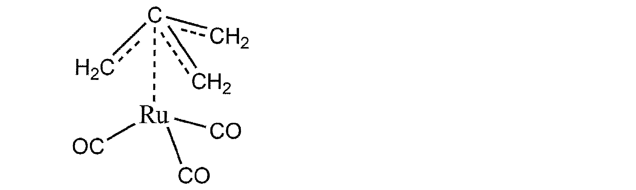
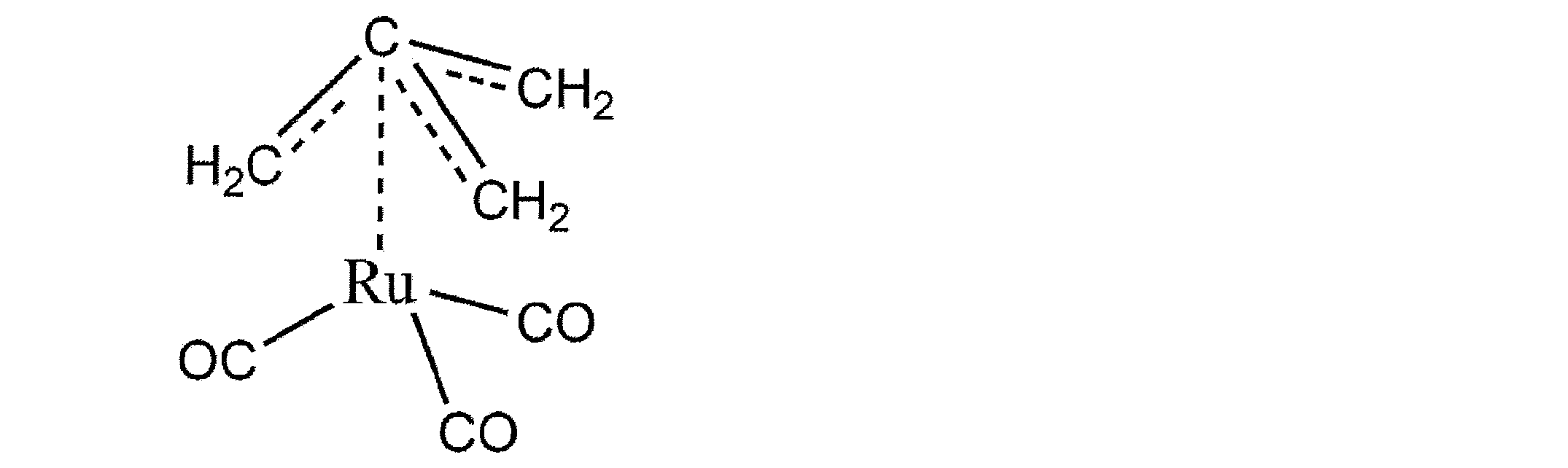
- the ruthenium precursor has the structure shown in Chemical formula 1 below.
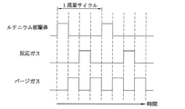
- the atomic layer deposition method is a method in which precursors and reaction gases are alternately supplied onto a substrate to form a thin film. After the supply of the precursor and the supply of the reaction gas, purge gas is supplied, respectively, and the precursor and the reaction gas remaining in the chamber are purged. When the precursor is supplied onto the substrate, the substrate and the precursor react with each other to form a layer of the precursor over the entire surface of the substrate. Once a layer of precursors is formed over the entire surface of the substrate, the additional precursors that are subsequently supplied are accumulated on the layer of the layer of precursors, even if the precursors are subsequently supplied. This accumulated precursor is removed by the purge gas supplied after the precursor is supplied. When supplying the reaction gas, a thin film is formed by the same mechanism.
- the reaction gas when the reaction gas is supplied to the precursor formed on the entire surface of the substrate, the reaction gas reacts with the precursor, and when all the reactions are completed, even if the reaction gas continues to be supplied, further reaction occurs. It disappears. Then, the residual reaction gas is removed by the purge gas supplied after the reaction gas is supplied.
- FIG. 1 shows tricarbonyl ( ⁇ 4 -methylene-1,3-propanediyl) ruthenium ( ⁇ 4 -methylene-1,3-propanedyl) ruthenium: C 7 H 6 O 3 Ru ((CO) 3 Ru-). It is a flowchart which shows the execution process of one Embodiment about the method of forming a ruthenium thin film using the ruthenium precursor expressed by TMM)).
- FIG. 2 is a diagram briefly showing a gas injection flow of an atomic layer deposition method in order to explain an embodiment of a method for forming a ruthenium thin film according to the present invention.
- the method for forming a ruthenium thin film first comprises tricarbonyl ( ⁇ 4 -methylene-1,3-propanediyl) ruthenium having the above-mentioned structure of Chemical formula 1.
- a ruthenium precursor represented by Tricarbonyl ( ⁇ 4 -methylene-1, 3-propanedyl) Ruthenium: C 7 H 6 O 3 Ru ((CO) 3 Ru-TMM)) is supplied onto a substrate (S110).
- the pressure for each chamber should be in the range of 0.1 to 10 Torr before the step of supplying the ruthenium precursor on the substrate. It is preferable to adjust to.
- the reaction gas supplied in the S130 step described later is hydrogen
- the pressure for each chamber is adjusted to be in the range of 10 to 50 Torr before the step of supplying the ruthenium precursor on the substrate. It is preferable to do so.
- Further inert gas can be supplied into the chamber to regulate the pressure in the chamber.
- the inert gas can be, but is not limited to, the same gas as the supplied purge gas in the S120 step or the S140 step.
- a preliminary cleaning step can be performed prior to the S110 step to remove etching residues or surface impurities that may be present on the substrate.
- a cleaning using argon (Ar) sputtering or a cleaning step using a wet detergent can be used.
- the ruthenium precursor is purged (S120).
- the purge gas it is preferable to use argon (Ar), helium (He), nitrogen (N 2 ) gas or the like. The purge gas removes residual by-products and unadsorbed ruthenium precursors.
- the reaction gas is supplied onto the substrate (S130).
- the reaction gas is a reducing gas that reduces the ruthenium precursor adsorbed on the substrate.
- the reaction gas is preferably one or more selected from the group consisting of oxygen (O 2 ), hydrogen (H 2 ), water (H 2 O) and ammonia (NH 3 ).
- oxygen or hydrogen is used, the formed ruthenium thin film has excellent characteristics, and these are preferable.
- the reaction gas is purged (S140).
- the purge gas it is preferable to use argon (Ar), helium (He), nitrogen (N 2 ) gas or the like.
- steps S110 to S140 are executed once in the above-mentioned order, and these form one vapor deposition cycle.
- This vapor deposition cycle can be repeated a plurality of times depending on the thickness of the target ruthenium thin film.
- a ruthenium thin film having a desired thickness is formed (S150)
- the step (S160) of heat-treating the ruthenium thin film can be performed at a temperature of 500 ° C. or lower in a hydrogen (H 2 ) atmosphere for about 10 minutes.
- FIG. 3 is a diagram showing the growth rate of the ruthenium thin film according to the ruthenium precursor supply time in the method for forming the ruthenium thin film using the atomic layer deposition method according to the present invention.
- FIG. 4 is a diagram showing the growth rate of the ruthenium thin film according to the gas supply time of the reaction gas in the ruthenium thin film forming method using the atomic layer deposition method according to the present invention.
- the ruthenium precursor was a ruthenium precursor having the structure of Chemical formula 1
- the reaction gas was oxygen gas
- the carrier gas and purge gas were nitrogen gas.
- the substrate temperature was maintained at 220 ° C. and the chamber pressure was 1 Torr.
- the purge gas was supplied for 10 seconds.
- the growth rate of the ruthenium thin film increases as each supply time increases until the ruthenium precursor supply time and the reaction gas supply time are set to 10 seconds.
- the ruthenium precursor supply time and the reaction gas supply time were 10 seconds or more, no increase in the growth rate of the ruthenium thin film was observed.
- the saturation time of the reaction step between the ruthenium precursor and the reaction gas is 10 seconds. Therefore, it is preferable to supply the ruthenium precursor and the reaction gas for 10 seconds in order to suppress waste of the ruthenium precursor and the reaction gas and to shorten the process time.
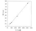
- FIG. 5 is a diagram showing the relationship between the number of vapor deposition cycles and the thickness of the thin film in the method for forming a ruthenium thin film using the atomic layer deposition method according to the present invention.
- the ruthenium precursor was a ruthenium precursor having the structure of Chemical formula 1
- the reaction gas was oxygen gas
- the carrier gas and purge gas were nitrogen gas.
- the chamber pressure was set to 1 Torr while the substrate temperature was maintained at 220 ° C. Then, the ruthenium precursor, the reaction gas and the purge gas were supplied for 10 seconds each.
- the vapor deposition thickness of the ruthenium thin film is constant at about 0.17 nm per vapor deposition cycle (S110 to S140). This shows a typical form of the atomic layer deposition method.
- the incubation cycle is very small, about 15 times, and it can be seen that the ruthenium precursor having the structure of Chemical formula 1 is a very suitable precursor for application to the atomic layer deposition method.
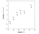
- FIG. 6 is a diagram showing the relationship between the vapor deposition temperature and the growth rate of the ruthenium thin film in the method for forming a ruthenium thin film using the atomic layer deposition method according to the present invention
- FIG. 7 is a diagram showing the relationship between the vapor deposition temperature and the growth rate of the ruthenium thin film. It is a figure which shows the relationship between the deposition temperature and the specific resistance of a ruthenium thin film in the method of forming a ruthenium thin film using the method.
- the ruthenium precursor was a ruthenium precursor having the structure of Chemical formula 1
- the reaction gas was oxygen gas
- the carrier gas and purge gas were nitrogen gas.
- the chamber pressure was 1 Torr.
- the ruthenium precursor, the reaction gas and the purge gas were supplied for 10 seconds each.
- the ruthenium precursor, the reaction gas and the purge gas were supplied for 10 seconds each.
- the growth rate is 1 ⁇ / cycle or higher, showing a very high growth rate.
- the vapor deposition temperature was 220 ° C. or higher, the growth rate was very high, about 1.5 ⁇ / cycle or higher.
- the ruthenium precursor having the structure of Chemical formula 1 does not thermally decompose at 260 ° C or lower, it exhibits a very high growth rate of 1.73 ⁇ / cycle at a vapor deposition temperature of 260 ° C even if thermal decomposition does not occur. It can be seen that the ruthenium precursor having the structure of Chemical formula 1 is a very excellent precursor for ruthenium thin film deposition.
- a ruthenium thin film having a very low resistivity value can be formed by using the ruthenium precursor having the structure of Chemical formula 1.
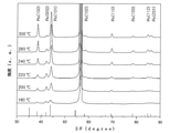
- FIG. 8 is a diagram showing the results of X-ray diffraction analysis (XRD) of the ruthenium thin film when the vapor deposition temperature is changed in the method for forming the ruthenium thin film using the atomic layer deposition method according to the present invention.
- XRD X-ray diffraction analysis
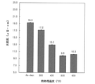
- FIG. 9 is a diagram showing the relationship between the heat treatment temperature after vapor deposition and the specific resistance of the ruthenium thin film in the ruthenium thin film forming method according to the present invention.
- FIG. 10 is a diagram showing the XRD result of the ruthenium thin film when the heat treatment temperature after vapor deposition is changed in the ruthenium thin film forming method according to the present invention.
- the ruthenium thin film immediately after vapor deposition (as-dep) was formed at a temperature of 220 ° C. using the ruthenium precursor having the structure of Chemical formula 1 and oxygen.
- the heat treatment after the vapor deposition was carried out in a hydrogen atmosphere for 10 minutes.
- the specific resistance of the ruthenium thin film decreases as the heat treatment temperature increases up to 500 ° C, but it may increase slightly at the heat treatment temperature of 600 ° C. I understand. Therefore, it can be said that the heat treatment after vapor deposition is preferably performed at a heat treatment temperature of 500 ° C. or lower.
- ruthenium thin film is less than 10 ⁇ ⁇ cm, which is about 9.8 ⁇ ⁇ cm, and an excellent ruthenium thin film that can be approximated to the bulk resistivity of ruthenium (7.1 ⁇ ⁇ cm). It turns out that it can be formed. That is, when the ruthenium thin film is formed by the method according to the present invention, it can be said that a ruthenium thin film having very excellent resistivity characteristics can be obtained even if a low temperature film forming step is applied.
- the present invention relates to tricarbonyl ( ⁇ 4 -methylene-1,3-propanediyl) ruthenium ( ⁇ 4 -methylene-1,3-propanedyl) ruthenium: C7 having the structure of Chemical formula 1 .
- This is a method of forming a ruthenium thin film by an atomic layer deposition method by applying a ruthenium precursor composed of H 6 O 3 Ru ((CO) 3 Ru-TMM)).
- a high quality ruthenium thin film having a low resistivity can be efficiently formed.
- the method for forming a ruthenium thin film of the present invention can also be applied to low temperature film formation.
- INDUSTRIAL APPLICABILITY The present invention is useful for wiring formation of semiconductor devices that are required to be further miniaturized in the future, and can contribute to miniaturization and high performance of various semiconductor devices.
Landscapes
- Chemical & Material Sciences (AREA)
- General Chemical & Material Sciences (AREA)
- Chemical Kinetics & Catalysis (AREA)
- Engineering & Computer Science (AREA)
- Materials Engineering (AREA)
- Mechanical Engineering (AREA)
- Metallurgy (AREA)
- Organic Chemistry (AREA)
- Chemical Vapour Deposition (AREA)
- Electrodes Of Semiconductors (AREA)
- Inorganic Compounds Of Heavy Metals (AREA)
Abstract
Description
[原子層蒸着法によるルテニウム薄膜の形成方法]
図1は、トリカルボニル(η4-メチレン-1,3-プロパンジイル)ルテニウム(Tricarbonyl(η4-methylene-1,3-propanediyl)Ruthenium:C7H6O3Ru((CO)3Ru-TMM))で表現されるルテニウム前駆体を利用して、ルテニウム薄膜を形成する方法について、その一実施形態の実行過程を概略的に示すフローチャートである。図2は、本発明に係るルテニウム薄膜の形成方法の一実施例を説明するため、原子層蒸着法のガス注入フローを簡単に示す図である。
次に、図3~図10を参照して、本発明の一実施形態に係るルテニウム薄膜の形成の結果を中心に、本発明を説明する。
Claims (8)
- ルテニウム前駆体を利用してルテニウム薄膜を形成するルテニウム薄膜形成方法において、
下記化1で示される構造を有するトリカルボニル(η4-メチレン-1,3-プロパンジイル)ルテニウム(Tricarbonyl(η4-methylene-1,3-propanediyl)Ruthenium((CO)3Ru-TMM))を前記ルテニウム前駆体とし、
前記ルテニウム前駆体と反応ガスを利用して、原子層蒸着法により200~350℃の範囲の温度でルテニウム薄膜を形成する段階を含むことを特徴とするルテニウム薄膜形成方法。
- 前記反応ガスは、酸素(O2)、水素(H2)、水(H2O)とアンモニア(NH3)からなる群から選択された一つ以上からなる請求項1に記載のルテニウム薄膜形成方法。
- 前記反応ガスは、酸素(O2)であり、0.1~10Torrの範囲の圧力で前記ルテニウム薄膜を形成する請求項2に記載のルテニウム薄膜形成方法。
- 前記反応ガスは、水素(H2)であり、10~50Torrの範囲の圧力で上記ルテニウム薄膜を形成する請求項2に記載のルテニウム薄膜形成方法。
- 前記ルテニウム薄膜の比抵抗は20μΩ・cm以下である請求項1~請求項4のいずれかに記載のルテニウム薄膜形成方法。
- 前記ルテニウム薄膜を形成する段階の後に、前記ルテニウム薄膜を熱処理する段階をさらに含む請求項1~請求項5のいずれかに記載のルテニウム薄膜形成方法。
- 前記熱処理する段階は、500℃以下の温度で行う請求項6に記載のルテニウム薄膜形成方法。
- 前記熱処理する段階で形成されたルテニウム薄膜の比抵抗は、10μΩ・cm以下である請求項6又は請求項7記載のルテニウム薄膜形成方法。
Priority Applications (4)
| Application Number | Priority Date | Filing Date | Title |
|---|---|---|---|
| CN202180058348.4A CN116097403B (zh) | 2020-08-04 | 2021-07-29 | 钌薄膜的形成方法 |
| US18/018,657 US12091748B2 (en) | 2020-08-04 | 2021-07-29 | Method for forming ruthenium thin film |
| JP2022541483A JP7611256B2 (ja) | 2020-08-04 | 2021-07-29 | ルテニウム薄膜の形成方法 |
| KR1020237005053A KR102800710B1 (ko) | 2020-08-04 | 2021-07-29 | 루테늄 박막의 형성 방법 |
Applications Claiming Priority (2)
| Application Number | Priority Date | Filing Date | Title |
|---|---|---|---|
| JP2020-132707 | 2020-08-04 | ||
| JP2020132707 | 2020-08-04 |
Publications (1)
| Publication Number | Publication Date |
|---|---|
| WO2022030348A1 true WO2022030348A1 (ja) | 2022-02-10 |
Family
ID=80118657
Family Applications (1)
| Application Number | Title | Priority Date | Filing Date |
|---|---|---|---|
| PCT/JP2021/028047 Ceased WO2022030348A1 (ja) | 2020-08-04 | 2021-07-29 | ルテニウム薄膜の形成方法 |
Country Status (6)
| Country | Link |
|---|---|
| US (1) | US12091748B2 (ja) |
| JP (1) | JP7611256B2 (ja) |
| KR (1) | KR102800710B1 (ja) |
| CN (1) | CN116097403B (ja) |
| TW (1) | TWI789848B (ja) |
| WO (1) | WO2022030348A1 (ja) |
Cited By (3)
| Publication number | Priority date | Publication date | Assignee | Title |
|---|---|---|---|---|
| WO2024090945A1 (ko) * | 2022-10-25 | 2024-05-02 | 주성엔지니어링(주) | 반도체 소자의 전극 형성 방법 |
| WO2024196152A1 (ko) * | 2023-03-20 | 2024-09-26 | 삼성전자주식회사 | 루테늄 함유 박막의 제조 방법 |
| WO2026028980A1 (ja) * | 2024-08-02 | 2026-02-05 | ユニスト(ウルサン ナショナル インスティテュート オブ サイエンス アンド テクノロジー) | ルテニウム薄膜の形成方法 |
Families Citing this family (1)
| Publication number | Priority date | Publication date | Assignee | Title |
|---|---|---|---|---|
| WO2024215025A2 (ko) * | 2023-04-13 | 2024-10-17 | 주성엔지니어링(주) | 산화 루테늄막의 형성 방법 및 이를 포함하는 반도체 소자의 제조 방법 |
Citations (3)
| Publication number | Priority date | Publication date | Assignee | Title |
|---|---|---|---|---|
| JP2002212112A (ja) * | 2001-01-22 | 2002-07-31 | Tanaka Kikinzoku Kogyo Kk | 化学気相蒸着用のルテニウム化合物並びにルテニウム薄膜及びルテニウム化合物薄膜の化学気相蒸着方法。 |
| JP2011522124A (ja) * | 2008-05-30 | 2011-07-28 | シグマ−アルドリッチ・カンパニー | 原子層堆積によるルテニウム含有膜を形成する方法 |
| JP2020090689A (ja) * | 2018-12-03 | 2020-06-11 | 田中貴金属工業株式会社 | ルテニウム錯体からなる化学蒸着用原料及び該化学蒸着用原料を用いた化学蒸着法 |
Family Cites Families (10)
| Publication number | Priority date | Publication date | Assignee | Title |
|---|---|---|---|---|
| US5962716A (en) | 1998-08-27 | 1999-10-05 | Micron Technology, Inc. | Methods for preparing ruthenium and osmium compounds |
| JP2000281694A (ja) | 1999-03-29 | 2000-10-10 | Tanaka Kikinzoku Kogyo Kk | 有機金属気相エピタキシー用の有機金属化合物 |
| US6303809B1 (en) | 1999-12-10 | 2001-10-16 | Yun Chi | Organometallic ruthenium and osmium source reagents for chemical vapor deposition |
| JP2013530304A (ja) * | 2010-04-19 | 2013-07-25 | レール・リキード−ソシエテ・アノニム・プール・レテュード・エ・レクスプロワタシオン・デ・プロセデ・ジョルジュ・クロード | Cvd及びald用のルテニウム含有前駆体 |
| JP4746141B1 (ja) | 2010-06-24 | 2011-08-10 | 田中貴金属工業株式会社 | 化学蒸着用の有機ルテニウム化合物及び該有機ルテニウム化合物を用いた化学蒸着方法 |
| TW201708579A (zh) * | 2015-08-27 | 2017-03-01 | 嶺南大學校產學協力團 | 藉由原子層蒸鍍法之釕薄膜之形成方法 |
| TWI809712B (zh) * | 2017-01-24 | 2023-07-21 | 美商應用材料股份有限公司 | 用於在基板上形成鈷層的方法 |
| KR101973549B1 (ko) * | 2017-04-19 | 2019-04-29 | 영남대학교 산학협력단 | 루테늄 박막 형성 방법 |
| TW202507047A (zh) * | 2017-11-01 | 2025-02-16 | 南韓商Dnf 有限公司 | 含釕薄膜之製造方法及以此方法製造之含釕薄膜 |
| WO2019088722A1 (ko) | 2017-11-01 | 2019-05-09 | (주)디엔에프 | 루테늄함유 박막의 제조방법 및 이로부터 제조된 루테늄함유 박막 |
-
2021
- 2021-07-28 TW TW110127741A patent/TWI789848B/zh active
- 2021-07-29 CN CN202180058348.4A patent/CN116097403B/zh active Active
- 2021-07-29 WO PCT/JP2021/028047 patent/WO2022030348A1/ja not_active Ceased
- 2021-07-29 JP JP2022541483A patent/JP7611256B2/ja active Active
- 2021-07-29 US US18/018,657 patent/US12091748B2/en active Active
- 2021-07-29 KR KR1020237005053A patent/KR102800710B1/ko active Active
Patent Citations (3)
| Publication number | Priority date | Publication date | Assignee | Title |
|---|---|---|---|---|
| JP2002212112A (ja) * | 2001-01-22 | 2002-07-31 | Tanaka Kikinzoku Kogyo Kk | 化学気相蒸着用のルテニウム化合物並びにルテニウム薄膜及びルテニウム化合物薄膜の化学気相蒸着方法。 |
| JP2011522124A (ja) * | 2008-05-30 | 2011-07-28 | シグマ−アルドリッチ・カンパニー | 原子層堆積によるルテニウム含有膜を形成する方法 |
| JP2020090689A (ja) * | 2018-12-03 | 2020-06-11 | 田中貴金属工業株式会社 | ルテニウム錯体からなる化学蒸着用原料及び該化学蒸着用原料を用いた化学蒸着法 |
Cited By (5)
| Publication number | Priority date | Publication date | Assignee | Title |
|---|---|---|---|---|
| WO2024090945A1 (ko) * | 2022-10-25 | 2024-05-02 | 주성엔지니어링(주) | 반도체 소자의 전극 형성 방법 |
| WO2024196152A1 (ko) * | 2023-03-20 | 2024-09-26 | 삼성전자주식회사 | 루테늄 함유 박막의 제조 방법 |
| WO2026028980A1 (ja) * | 2024-08-02 | 2026-02-05 | ユニスト(ウルサン ナショナル インスティテュート オブ サイエンス アンド テクノロジー) | ルテニウム薄膜の形成方法 |
| JP2026025068A (ja) * | 2024-08-02 | 2026-02-13 | ユニスト(ウルサン ナショナル インスティテュート オブ サイエンス アンド テクノロジー) | ルテニウム薄膜の形成方法 |
| JP7829891B2 (ja) | 2024-08-02 | 2026-03-16 | ユニスト(ウルサン ナショナル インスティテュート オブ サイエンス アンド テクノロジー) | ルテニウム薄膜の形成方法 |
Also Published As
| Publication number | Publication date |
|---|---|
| JP7611256B2 (ja) | 2025-01-09 |
| US12091748B2 (en) | 2024-09-17 |
| KR102800710B1 (ko) | 2025-04-29 |
| US20230212741A1 (en) | 2023-07-06 |
| TWI789848B (zh) | 2023-01-11 |
| JPWO2022030348A1 (ja) | 2022-02-10 |
| KR20230038543A (ko) | 2023-03-20 |
| CN116097403B (zh) | 2025-05-09 |
| CN116097403A (zh) | 2023-05-09 |
| TW202225449A (zh) | 2022-07-01 |
Similar Documents
| Publication | Publication Date | Title |
|---|---|---|
| US11174550B2 (en) | Selective deposition on metal or metallic surfaces relative to dielectric surfaces | |
| WO2022030348A1 (ja) | ルテニウム薄膜の形成方法 | |
| TWI394858B (zh) | 用於沉積具有降低電阻率及改良表面形態之鎢膜的方法 | |
| KR102013927B1 (ko) | 평활한 금속 질화물 막들의 퇴적 | |
| TWI661080B (zh) | 金屬矽化物的選擇性形成 | |
| KR101188503B1 (ko) | 카보닐 원료를 사용한 금속막의 성막 방법, 다층 배선 구조의 형성 방법, 반도체 장치의 제조 방법 및 성막 장치 | |
| TWI798582B (zh) | 第六族金屬沈積方法 | |
| JP2018178259A (ja) | ルテニウム薄膜形成方法 | |
| US20200090991A1 (en) | Method Of Forming Via With Embedded Barrier | |
| CN110777351B (zh) | 钨沉积方法 | |
| KR102837501B1 (ko) | 초박형 금속 박막의 제조 방법 및 제조 장치 | |
| CN120924935A (zh) | 包含金的薄膜的气相沉积 | |
| TW202407132A (zh) | 包含貴金屬之材料的選擇性沉積 | |
| TWI515803B (zh) | 矽化鉭內的摻雜鋁 | |
| WO2017009948A1 (ja) | 原子層蒸着法によるルテニウム薄膜の形成方法 | |
| US12622243B2 (en) | Selective liner deposition for via resistance reduction | |
| KR102536802B1 (ko) | 루테늄 박막의 선택적 증착 방법 | |
| US20240420997A1 (en) | Selective liner deposition for via resistance reduction | |
| JP5054890B2 (ja) | 半導体装置の製造方法 | |
| TW201708579A (zh) | 藉由原子層蒸鍍法之釕薄膜之形成方法 | |
| JP2026025068A (ja) | ルテニウム薄膜の形成方法 | |
| CN118064870A (zh) | 利用化学净化物质的薄膜形成方法 | |
| CN120249935A (zh) | 用于区域选择性沉积的方法和设备 | |
| JP2024513402A (ja) | 低温堆積プロセス | |
| KR20100023329A (ko) | 금속막 형성 방법 |
Legal Events
| Date | Code | Title | Description |
|---|---|---|---|
| 121 | Ep: the epo has been informed by wipo that ep was designated in this application |
Ref document number: 21854609 Country of ref document: EP Kind code of ref document: A1 |
|
| ENP | Entry into the national phase |
Ref document number: 2022541483 Country of ref document: JP Kind code of ref document: A |
|
| ENP | Entry into the national phase |
Ref document number: 20237005053 Country of ref document: KR Kind code of ref document: A |
|
| NENP | Non-entry into the national phase |
Ref country code: DE |
|
| 122 | Ep: pct application non-entry in european phase |
Ref document number: 21854609 Country of ref document: EP Kind code of ref document: A1 |
|
| WWG | Wipo information: grant in national office |
Ref document number: 202180058348.4 Country of ref document: CN |