WO2022030114A1 - 半導体積層体、半導体素子および半導体素子の製造方法 - Google Patents
半導体積層体、半導体素子および半導体素子の製造方法 Download PDFInfo
- Publication number
- WO2022030114A1 WO2022030114A1 PCT/JP2021/023252 JP2021023252W WO2022030114A1 WO 2022030114 A1 WO2022030114 A1 WO 2022030114A1 JP 2021023252 W JP2021023252 W JP 2021023252W WO 2022030114 A1 WO2022030114 A1 WO 2022030114A1
- Authority
- WO
- WIPO (PCT)
- Prior art keywords
- metal oxide
- buffer
- oxide semiconductor
- buffer layer
- crystalline metal
- Prior art date
Links
- 239000004065 semiconductor Substances 0.000 title claims abstract description 220
- 238000004519 manufacturing process Methods 0.000 title claims description 19
- 229910044991 metal oxide Inorganic materials 0.000 claims abstract description 100
- 150000004706 metal oxides Chemical class 0.000 claims abstract description 100
- 239000000758 substrate Substances 0.000 claims abstract description 77
- 229910052751 metal Inorganic materials 0.000 claims abstract description 54
- 239000002184 metal Substances 0.000 claims abstract description 43
- 239000000203 mixture Substances 0.000 claims abstract description 35
- 239000010431 corundum Substances 0.000 claims abstract description 12
- 229910052593 corundum Inorganic materials 0.000 claims abstract description 12
- 238000000034 method Methods 0.000 claims description 30
- 229910052782 aluminium Inorganic materials 0.000 claims description 8
- XAGFODPZIPBFFR-UHFFFAOYSA-N aluminium Chemical group [Al] XAGFODPZIPBFFR-UHFFFAOYSA-N 0.000 claims description 8
- GYHNNYVSQQEPJS-UHFFFAOYSA-N Gallium Chemical group [Ga] GYHNNYVSQQEPJS-UHFFFAOYSA-N 0.000 claims description 5
- 229910052733 gallium Inorganic materials 0.000 claims description 5
- 230000007423 decrease Effects 0.000 claims 1
- 230000007547 defect Effects 0.000 abstract description 14
- 230000015572 biosynthetic process Effects 0.000 abstract description 2
- 239000010410 layer Substances 0.000 description 115
- 239000013078 crystal Substances 0.000 description 17
- 229910005191 Ga 2 O 3 Inorganic materials 0.000 description 10
- IJGRMHOSHXDMSA-UHFFFAOYSA-N Atomic nitrogen Chemical compound N#N IJGRMHOSHXDMSA-UHFFFAOYSA-N 0.000 description 7
- XEEYBQQBJWHFJM-UHFFFAOYSA-N Iron Chemical compound [Fe] XEEYBQQBJWHFJM-UHFFFAOYSA-N 0.000 description 7
- 230000000052 comparative effect Effects 0.000 description 7
- 229910001873 dinitrogen Inorganic materials 0.000 description 7
- XLOMVQKBTHCTTD-UHFFFAOYSA-N Zinc monoxide Chemical compound [Zn]=O XLOMVQKBTHCTTD-UHFFFAOYSA-N 0.000 description 6
- 238000005229 chemical vapour deposition Methods 0.000 description 6
- 230000000694 effects Effects 0.000 description 6
- 238000011156 evaluation Methods 0.000 description 6
- 239000003595 mist Substances 0.000 description 6
- 239000002243 precursor Substances 0.000 description 6
- 238000002441 X-ray diffraction Methods 0.000 description 5
- 239000000463 material Substances 0.000 description 5
- 239000010453 quartz Substances 0.000 description 5
- 229910052594 sapphire Inorganic materials 0.000 description 5
- 239000010980 sapphire Substances 0.000 description 5
- VYPSYNLAJGMNEJ-UHFFFAOYSA-N silicon dioxide Inorganic materials O=[Si]=O VYPSYNLAJGMNEJ-UHFFFAOYSA-N 0.000 description 5
- 239000010936 titanium Substances 0.000 description 5
- 235000012431 wafers Nutrition 0.000 description 5
- VEXZGXHMUGYJMC-UHFFFAOYSA-N Hydrochloric acid Chemical compound Cl VEXZGXHMUGYJMC-UHFFFAOYSA-N 0.000 description 4
- PXHVJJICTQNCMI-UHFFFAOYSA-N Nickel Chemical compound [Ni] PXHVJJICTQNCMI-UHFFFAOYSA-N 0.000 description 4
- KDLHZDBZIXYQEI-UHFFFAOYSA-N Palladium Chemical compound [Pd] KDLHZDBZIXYQEI-UHFFFAOYSA-N 0.000 description 4
- RTAQQCXQSZGOHL-UHFFFAOYSA-N Titanium Chemical compound [Ti] RTAQQCXQSZGOHL-UHFFFAOYSA-N 0.000 description 4
- 239000011651 chromium Substances 0.000 description 4
- 230000005669 field effect Effects 0.000 description 4
- 239000012535 impurity Substances 0.000 description 4
- 229910052738 indium Inorganic materials 0.000 description 4
- APFVFJFRJDLVQX-UHFFFAOYSA-N indium atom Chemical compound [In] APFVFJFRJDLVQX-UHFFFAOYSA-N 0.000 description 4
- BASFCYQUMIYNBI-UHFFFAOYSA-N platinum Chemical compound [Pt] BASFCYQUMIYNBI-UHFFFAOYSA-N 0.000 description 4
- 238000004544 sputter deposition Methods 0.000 description 4
- 229910052719 titanium Inorganic materials 0.000 description 4
- VYZAMTAEIAYCRO-UHFFFAOYSA-N Chromium Chemical compound [Cr] VYZAMTAEIAYCRO-UHFFFAOYSA-N 0.000 description 3
- RYGMFSIKBFXOCR-UHFFFAOYSA-N Copper Chemical compound [Cu] RYGMFSIKBFXOCR-UHFFFAOYSA-N 0.000 description 3
- ATJFFYVFTNAWJD-UHFFFAOYSA-N Tin Chemical compound [Sn] ATJFFYVFTNAWJD-UHFFFAOYSA-N 0.000 description 3
- 229910052804 chromium Inorganic materials 0.000 description 3
- 239000004020 conductor Substances 0.000 description 3
- 229910052802 copper Inorganic materials 0.000 description 3
- 239000010949 copper Substances 0.000 description 3
- AMGQUBHHOARCQH-UHFFFAOYSA-N indium;oxotin Chemical compound [In].[Sn]=O AMGQUBHHOARCQH-UHFFFAOYSA-N 0.000 description 3
- 239000012212 insulator Substances 0.000 description 3
- 229910052741 iridium Inorganic materials 0.000 description 3
- GKOZUEZYRPOHIO-UHFFFAOYSA-N iridium atom Chemical compound [Ir] GKOZUEZYRPOHIO-UHFFFAOYSA-N 0.000 description 3
- 229910052742 iron Inorganic materials 0.000 description 3
- 150000002739 metals Chemical class 0.000 description 3
- 229910052718 tin Inorganic materials 0.000 description 3
- 239000011135 tin Substances 0.000 description 3
- 229910052720 vanadium Inorganic materials 0.000 description 3
- GPPXJZIENCGNKB-UHFFFAOYSA-N vanadium Chemical compound [V]#[V] GPPXJZIENCGNKB-UHFFFAOYSA-N 0.000 description 3
- 239000011787 zinc oxide Substances 0.000 description 3
- 229910018072 Al 2 O 3 Inorganic materials 0.000 description 2
- ZOKXTWBITQBERF-UHFFFAOYSA-N Molybdenum Chemical compound [Mo] ZOKXTWBITQBERF-UHFFFAOYSA-N 0.000 description 2
- 229910052779 Neodymium Inorganic materials 0.000 description 2
- BQCADISMDOOEFD-UHFFFAOYSA-N Silver Chemical compound [Ag] BQCADISMDOOEFD-UHFFFAOYSA-N 0.000 description 2
- HCHKCACWOHOZIP-UHFFFAOYSA-N Zinc Chemical compound [Zn] HCHKCACWOHOZIP-UHFFFAOYSA-N 0.000 description 2
- QCWXUUIWCKQGHC-UHFFFAOYSA-N Zirconium Chemical compound [Zr] QCWXUUIWCKQGHC-UHFFFAOYSA-N 0.000 description 2
- 229910045601 alloy Inorganic materials 0.000 description 2
- 239000000956 alloy Substances 0.000 description 2
- 239000007864 aqueous solution Substances 0.000 description 2
- 238000001505 atmospheric-pressure chemical vapour deposition Methods 0.000 description 2
- 230000004888 barrier function Effects 0.000 description 2
- 229910017052 cobalt Inorganic materials 0.000 description 2
- 239000010941 cobalt Substances 0.000 description 2
- GUTLYIVDDKVIGB-UHFFFAOYSA-N cobalt atom Chemical compound [Co] GUTLYIVDDKVIGB-UHFFFAOYSA-N 0.000 description 2
- 150000001875 compounds Chemical class 0.000 description 2
- AJNVQOSZGJRYEI-UHFFFAOYSA-N digallium;oxygen(2-) Chemical compound [O-2].[O-2].[O-2].[Ga+3].[Ga+3] AJNVQOSZGJRYEI-UHFFFAOYSA-N 0.000 description 2
- 239000007772 electrode material Substances 0.000 description 2
- PCHJSUWPFVWCPO-UHFFFAOYSA-N gold Chemical compound [Au] PCHJSUWPFVWCPO-UHFFFAOYSA-N 0.000 description 2
- 229910052737 gold Inorganic materials 0.000 description 2
- 239000010931 gold Substances 0.000 description 2
- 229910052735 hafnium Inorganic materials 0.000 description 2
- VBJZVLUMGGDVMO-UHFFFAOYSA-N hafnium atom Chemical compound [Hf] VBJZVLUMGGDVMO-UHFFFAOYSA-N 0.000 description 2
- 238000002248 hydride vapour-phase epitaxy Methods 0.000 description 2
- 229910003437 indium oxide Inorganic materials 0.000 description 2
- PJXISJQVUVHSOJ-UHFFFAOYSA-N indium(iii) oxide Chemical compound [O-2].[O-2].[O-2].[In+3].[In+3] PJXISJQVUVHSOJ-UHFFFAOYSA-N 0.000 description 2
- 238000007733 ion plating Methods 0.000 description 2
- WPBNNNQJVZRUHP-UHFFFAOYSA-L manganese(2+);methyl n-[[2-(methoxycarbonylcarbamothioylamino)phenyl]carbamothioyl]carbamate;n-[2-(sulfidocarbothioylamino)ethyl]carbamodithioate Chemical compound [Mn+2].[S-]C(=S)NCCNC([S-])=S.COC(=O)NC(=S)NC1=CC=CC=C1NC(=S)NC(=O)OC WPBNNNQJVZRUHP-UHFFFAOYSA-L 0.000 description 2
- 239000012528 membrane Substances 0.000 description 2
- 229910052750 molybdenum Inorganic materials 0.000 description 2
- 239000011733 molybdenum Substances 0.000 description 2
- QEFYFXOXNSNQGX-UHFFFAOYSA-N neodymium atom Chemical compound [Nd] QEFYFXOXNSNQGX-UHFFFAOYSA-N 0.000 description 2
- 229910052759 nickel Inorganic materials 0.000 description 2
- 229910052758 niobium Inorganic materials 0.000 description 2
- 239000010955 niobium Substances 0.000 description 2
- GUCVJGMIXFAOAE-UHFFFAOYSA-N niobium atom Chemical compound [Nb] GUCVJGMIXFAOAE-UHFFFAOYSA-N 0.000 description 2
- 229910052763 palladium Inorganic materials 0.000 description 2
- 238000005268 plasma chemical vapour deposition Methods 0.000 description 2
- 229910052697 platinum Inorganic materials 0.000 description 2
- 229920000767 polyaniline Polymers 0.000 description 2
- 229920000128 polypyrrole Polymers 0.000 description 2
- 229920000123 polythiophene Polymers 0.000 description 2
- -1 renium oxide Chemical compound 0.000 description 2
- 239000010948 rhodium Substances 0.000 description 2
- 229910052709 silver Inorganic materials 0.000 description 2
- 239000004332 silver Substances 0.000 description 2
- 229910052715 tantalum Inorganic materials 0.000 description 2
- GUVRBAGPIYLISA-UHFFFAOYSA-N tantalum atom Chemical compound [Ta] GUVRBAGPIYLISA-UHFFFAOYSA-N 0.000 description 2
- XOLBLPGZBRYERU-UHFFFAOYSA-N tin dioxide Chemical compound O=[Sn]=O XOLBLPGZBRYERU-UHFFFAOYSA-N 0.000 description 2
- 229910001887 tin oxide Inorganic materials 0.000 description 2
- WFKWXMTUELFFGS-UHFFFAOYSA-N tungsten Chemical compound [W] WFKWXMTUELFFGS-UHFFFAOYSA-N 0.000 description 2
- 229910052721 tungsten Inorganic materials 0.000 description 2
- 239000010937 tungsten Substances 0.000 description 2
- 238000007740 vapor deposition Methods 0.000 description 2
- 229910052725 zinc Inorganic materials 0.000 description 2
- 239000011701 zinc Substances 0.000 description 2
- 229910052726 zirconium Inorganic materials 0.000 description 2
- ZVYYAYJIGYODSD-LNTINUHCSA-K (z)-4-bis[[(z)-4-oxopent-2-en-2-yl]oxy]gallanyloxypent-3-en-2-one Chemical compound [Ga+3].C\C([O-])=C\C(C)=O.C\C([O-])=C\C(C)=O.C\C([O-])=C\C(C)=O ZVYYAYJIGYODSD-LNTINUHCSA-K 0.000 description 1
- XBIUWALDKXACEA-UHFFFAOYSA-N 3-[bis(2,4-dioxopentan-3-yl)alumanyl]pentane-2,4-dione Chemical compound CC(=O)C(C(C)=O)[Al](C(C(C)=O)C(C)=O)C(C(C)=O)C(C)=O XBIUWALDKXACEA-UHFFFAOYSA-N 0.000 description 1
- FYYHWMGAXLPEAU-UHFFFAOYSA-N Magnesium Chemical compound [Mg] FYYHWMGAXLPEAU-UHFFFAOYSA-N 0.000 description 1
- XUIMIQQOPSSXEZ-UHFFFAOYSA-N Silicon Chemical compound [Si] XUIMIQQOPSSXEZ-UHFFFAOYSA-N 0.000 description 1
- 229910006404 SnO 2 Inorganic materials 0.000 description 1
- 238000000137 annealing Methods 0.000 description 1
- 238000000576 coating method Methods 0.000 description 1
- 230000006837 decompression Effects 0.000 description 1
- 238000010586 diagram Methods 0.000 description 1
- 239000002019 doping agent Substances 0.000 description 1
- 239000012467 final product Substances 0.000 description 1
- 239000000446 fuel Substances 0.000 description 1
- 229910001195 gallium oxide Inorganic materials 0.000 description 1
- 239000007789 gas Substances 0.000 description 1
- 229910052732 germanium Inorganic materials 0.000 description 1
- GNPVGFCGXDBREM-UHFFFAOYSA-N germanium atom Chemical compound [Ge] GNPVGFCGXDBREM-UHFFFAOYSA-N 0.000 description 1
- 238000010438 heat treatment Methods 0.000 description 1
- 150000004678 hydrides Chemical class 0.000 description 1
- 238000009413 insulation Methods 0.000 description 1
- 238000010030 laminating Methods 0.000 description 1
- 238000004518 low pressure chemical vapour deposition Methods 0.000 description 1
- 239000011777 magnesium Substances 0.000 description 1
- 229910052749 magnesium Inorganic materials 0.000 description 1
- 230000003287 optical effect Effects 0.000 description 1
- 238000000059 patterning Methods 0.000 description 1
- 238000000206 photolithography Methods 0.000 description 1
- 238000000053 physical method Methods 0.000 description 1
- 230000000644 propagated effect Effects 0.000 description 1
- 229910052703 rhodium Inorganic materials 0.000 description 1
- MHOVAHRLVXNVSD-UHFFFAOYSA-N rhodium atom Chemical compound [Rh] MHOVAHRLVXNVSD-UHFFFAOYSA-N 0.000 description 1
- 229910052710 silicon Inorganic materials 0.000 description 1
- 239000010703 silicon Substances 0.000 description 1
- 239000002356 single layer Substances 0.000 description 1
- 239000007921 spray Substances 0.000 description 1
- 239000000126 substance Substances 0.000 description 1
- XLYOFNOQVPJJNP-UHFFFAOYSA-N water Substances O XLYOFNOQVPJJNP-UHFFFAOYSA-N 0.000 description 1
- YVTHLONGBIQYBO-UHFFFAOYSA-N zinc indium(3+) oxygen(2-) Chemical compound [O--].[Zn++].[In+3] YVTHLONGBIQYBO-UHFFFAOYSA-N 0.000 description 1
Images


Classifications
-
- H—ELECTRICITY
- H01—ELECTRIC ELEMENTS
- H01L—SEMICONDUCTOR DEVICES NOT COVERED BY CLASS H10
- H01L21/00—Processes or apparatus adapted for the manufacture or treatment of semiconductor or solid state devices or of parts thereof
- H01L21/02—Manufacture or treatment of semiconductor devices or of parts thereof
- H01L21/02104—Forming layers
- H01L21/02365—Forming inorganic semiconducting materials on a substrate
- H01L21/02436—Intermediate layers between substrates and deposited layers
- H01L21/02494—Structure
- H01L21/02496—Layer structure
- H01L21/02505—Layer structure consisting of more than two layers
-
- C—CHEMISTRY; METALLURGY
- C23—COATING METALLIC MATERIAL; COATING MATERIAL WITH METALLIC MATERIAL; CHEMICAL SURFACE TREATMENT; DIFFUSION TREATMENT OF METALLIC MATERIAL; COATING BY VACUUM EVAPORATION, BY SPUTTERING, BY ION IMPLANTATION OR BY CHEMICAL VAPOUR DEPOSITION, IN GENERAL; INHIBITING CORROSION OF METALLIC MATERIAL OR INCRUSTATION IN GENERAL
- C23C—COATING METALLIC MATERIAL; COATING MATERIAL WITH METALLIC MATERIAL; SURFACE TREATMENT OF METALLIC MATERIAL BY DIFFUSION INTO THE SURFACE, BY CHEMICAL CONVERSION OR SUBSTITUTION; COATING BY VACUUM EVAPORATION, BY SPUTTERING, BY ION IMPLANTATION OR BY CHEMICAL VAPOUR DEPOSITION, IN GENERAL
- C23C16/00—Chemical coating by decomposition of gaseous compounds, without leaving reaction products of surface material in the coating, i.e. chemical vapour deposition [CVD] processes
- C23C16/22—Chemical coating by decomposition of gaseous compounds, without leaving reaction products of surface material in the coating, i.e. chemical vapour deposition [CVD] processes characterised by the deposition of inorganic material, other than metallic material
- C23C16/30—Deposition of compounds, mixtures or solid solutions, e.g. borides, carbides, nitrides
- C23C16/40—Oxides
-
- C—CHEMISTRY; METALLURGY
- C23—COATING METALLIC MATERIAL; COATING MATERIAL WITH METALLIC MATERIAL; CHEMICAL SURFACE TREATMENT; DIFFUSION TREATMENT OF METALLIC MATERIAL; COATING BY VACUUM EVAPORATION, BY SPUTTERING, BY ION IMPLANTATION OR BY CHEMICAL VAPOUR DEPOSITION, IN GENERAL; INHIBITING CORROSION OF METALLIC MATERIAL OR INCRUSTATION IN GENERAL
- C23C—COATING METALLIC MATERIAL; COATING MATERIAL WITH METALLIC MATERIAL; SURFACE TREATMENT OF METALLIC MATERIAL BY DIFFUSION INTO THE SURFACE, BY CHEMICAL CONVERSION OR SUBSTITUTION; COATING BY VACUUM EVAPORATION, BY SPUTTERING, BY ION IMPLANTATION OR BY CHEMICAL VAPOUR DEPOSITION, IN GENERAL
- C23C16/00—Chemical coating by decomposition of gaseous compounds, without leaving reaction products of surface material in the coating, i.e. chemical vapour deposition [CVD] processes
- C23C16/44—Chemical coating by decomposition of gaseous compounds, without leaving reaction products of surface material in the coating, i.e. chemical vapour deposition [CVD] processes characterised by the method of coating
- C23C16/448—Chemical coating by decomposition of gaseous compounds, without leaving reaction products of surface material in the coating, i.e. chemical vapour deposition [CVD] processes characterised by the method of coating characterised by the method used for generating reactive gas streams, e.g. by evaporation or sublimation of precursor materials
-
- C—CHEMISTRY; METALLURGY
- C30—CRYSTAL GROWTH
- C30B—SINGLE-CRYSTAL GROWTH; UNIDIRECTIONAL SOLIDIFICATION OF EUTECTIC MATERIAL OR UNIDIRECTIONAL DEMIXING OF EUTECTOID MATERIAL; REFINING BY ZONE-MELTING OF MATERIAL; PRODUCTION OF A HOMOGENEOUS POLYCRYSTALLINE MATERIAL WITH DEFINED STRUCTURE; SINGLE CRYSTALS OR HOMOGENEOUS POLYCRYSTALLINE MATERIAL WITH DEFINED STRUCTURE; AFTER-TREATMENT OF SINGLE CRYSTALS OR A HOMOGENEOUS POLYCRYSTALLINE MATERIAL WITH DEFINED STRUCTURE; APPARATUS THEREFOR
- C30B25/00—Single-crystal growth by chemical reaction of reactive gases, e.g. chemical vapour-deposition growth
- C30B25/02—Epitaxial-layer growth
- C30B25/04—Pattern deposit, e.g. by using masks
-
- C—CHEMISTRY; METALLURGY
- C30—CRYSTAL GROWTH
- C30B—SINGLE-CRYSTAL GROWTH; UNIDIRECTIONAL SOLIDIFICATION OF EUTECTIC MATERIAL OR UNIDIRECTIONAL DEMIXING OF EUTECTOID MATERIAL; REFINING BY ZONE-MELTING OF MATERIAL; PRODUCTION OF A HOMOGENEOUS POLYCRYSTALLINE MATERIAL WITH DEFINED STRUCTURE; SINGLE CRYSTALS OR HOMOGENEOUS POLYCRYSTALLINE MATERIAL WITH DEFINED STRUCTURE; AFTER-TREATMENT OF SINGLE CRYSTALS OR A HOMOGENEOUS POLYCRYSTALLINE MATERIAL WITH DEFINED STRUCTURE; APPARATUS THEREFOR
- C30B25/00—Single-crystal growth by chemical reaction of reactive gases, e.g. chemical vapour-deposition growth
- C30B25/02—Epitaxial-layer growth
- C30B25/18—Epitaxial-layer growth characterised by the substrate
- C30B25/183—Epitaxial-layer growth characterised by the substrate being provided with a buffer layer, e.g. a lattice matching layer
-
- C—CHEMISTRY; METALLURGY
- C30—CRYSTAL GROWTH
- C30B—SINGLE-CRYSTAL GROWTH; UNIDIRECTIONAL SOLIDIFICATION OF EUTECTIC MATERIAL OR UNIDIRECTIONAL DEMIXING OF EUTECTOID MATERIAL; REFINING BY ZONE-MELTING OF MATERIAL; PRODUCTION OF A HOMOGENEOUS POLYCRYSTALLINE MATERIAL WITH DEFINED STRUCTURE; SINGLE CRYSTALS OR HOMOGENEOUS POLYCRYSTALLINE MATERIAL WITH DEFINED STRUCTURE; AFTER-TREATMENT OF SINGLE CRYSTALS OR A HOMOGENEOUS POLYCRYSTALLINE MATERIAL WITH DEFINED STRUCTURE; APPARATUS THEREFOR
- C30B29/00—Single crystals or homogeneous polycrystalline material with defined structure characterised by the material or by their shape
- C30B29/10—Inorganic compounds or compositions
- C30B29/16—Oxides
-
- H—ELECTRICITY
- H01—ELECTRIC ELEMENTS
- H01L—SEMICONDUCTOR DEVICES NOT COVERED BY CLASS H10
- H01L21/00—Processes or apparatus adapted for the manufacture or treatment of semiconductor or solid state devices or of parts thereof
- H01L21/02—Manufacture or treatment of semiconductor devices or of parts thereof
- H01L21/02104—Forming layers
- H01L21/02365—Forming inorganic semiconducting materials on a substrate
- H01L21/02367—Substrates
- H01L21/0237—Materials
- H01L21/0242—Crystalline insulating materials
-
- H—ELECTRICITY
- H01—ELECTRIC ELEMENTS
- H01L—SEMICONDUCTOR DEVICES NOT COVERED BY CLASS H10
- H01L21/00—Processes or apparatus adapted for the manufacture or treatment of semiconductor or solid state devices or of parts thereof
- H01L21/02—Manufacture or treatment of semiconductor devices or of parts thereof
- H01L21/02104—Forming layers
- H01L21/02365—Forming inorganic semiconducting materials on a substrate
- H01L21/02436—Intermediate layers between substrates and deposited layers
- H01L21/02439—Materials
- H01L21/02483—Oxide semiconducting materials not being Group 12/16 materials, e.g. ternary compounds
-
- H—ELECTRICITY
- H01—ELECTRIC ELEMENTS
- H01L—SEMICONDUCTOR DEVICES NOT COVERED BY CLASS H10
- H01L21/00—Processes or apparatus adapted for the manufacture or treatment of semiconductor or solid state devices or of parts thereof
- H01L21/02—Manufacture or treatment of semiconductor devices or of parts thereof
- H01L21/02104—Forming layers
- H01L21/02365—Forming inorganic semiconducting materials on a substrate
- H01L21/02436—Intermediate layers between substrates and deposited layers
- H01L21/02494—Structure
- H01L21/02496—Layer structure
- H01L21/0251—Graded layers
-
- H—ELECTRICITY
- H01—ELECTRIC ELEMENTS
- H01L—SEMICONDUCTOR DEVICES NOT COVERED BY CLASS H10
- H01L21/00—Processes or apparatus adapted for the manufacture or treatment of semiconductor or solid state devices or of parts thereof
- H01L21/02—Manufacture or treatment of semiconductor devices or of parts thereof
- H01L21/02104—Forming layers
- H01L21/02365—Forming inorganic semiconducting materials on a substrate
- H01L21/02518—Deposited layers
- H01L21/02521—Materials
- H01L21/02565—Oxide semiconducting materials not being Group 12/16 materials, e.g. ternary compounds
-
- H—ELECTRICITY
- H01—ELECTRIC ELEMENTS
- H01L—SEMICONDUCTOR DEVICES NOT COVERED BY CLASS H10
- H01L21/00—Processes or apparatus adapted for the manufacture or treatment of semiconductor or solid state devices or of parts thereof
- H01L21/02—Manufacture or treatment of semiconductor devices or of parts thereof
- H01L21/02104—Forming layers
- H01L21/02365—Forming inorganic semiconducting materials on a substrate
- H01L21/02612—Formation types
- H01L21/02617—Deposition types
- H01L21/02623—Liquid deposition
- H01L21/02628—Liquid deposition using solutions
-
- H—ELECTRICITY
- H01—ELECTRIC ELEMENTS
- H01L—SEMICONDUCTOR DEVICES NOT COVERED BY CLASS H10
- H01L29/00—Semiconductor devices specially adapted for rectifying, amplifying, oscillating or switching and having potential barriers; Capacitors or resistors having potential barriers, e.g. a PN-junction depletion layer or carrier concentration layer; Details of semiconductor bodies or of electrodes thereof ; Multistep manufacturing processes therefor
- H01L29/02—Semiconductor bodies ; Multistep manufacturing processes therefor
- H01L29/04—Semiconductor bodies ; Multistep manufacturing processes therefor characterised by their crystalline structure, e.g. polycrystalline, cubic or particular orientation of crystalline planes
-
- H—ELECTRICITY
- H01—ELECTRIC ELEMENTS
- H01L—SEMICONDUCTOR DEVICES NOT COVERED BY CLASS H10
- H01L29/00—Semiconductor devices specially adapted for rectifying, amplifying, oscillating or switching and having potential barriers; Capacitors or resistors having potential barriers, e.g. a PN-junction depletion layer or carrier concentration layer; Details of semiconductor bodies or of electrodes thereof ; Multistep manufacturing processes therefor
- H01L29/02—Semiconductor bodies ; Multistep manufacturing processes therefor
- H01L29/12—Semiconductor bodies ; Multistep manufacturing processes therefor characterised by the materials of which they are formed
- H01L29/24—Semiconductor bodies ; Multistep manufacturing processes therefor characterised by the materials of which they are formed including, apart from doping materials or other impurities, only semiconductor materials not provided for in groups H01L29/16, H01L29/18, H01L29/20, H01L29/22
-
- H—ELECTRICITY
- H01—ELECTRIC ELEMENTS
- H01L—SEMICONDUCTOR DEVICES NOT COVERED BY CLASS H10
- H01L29/00—Semiconductor devices specially adapted for rectifying, amplifying, oscillating or switching and having potential barriers; Capacitors or resistors having potential barriers, e.g. a PN-junction depletion layer or carrier concentration layer; Details of semiconductor bodies or of electrodes thereof ; Multistep manufacturing processes therefor
- H01L29/40—Electrodes ; Multistep manufacturing processes therefor
- H01L29/43—Electrodes ; Multistep manufacturing processes therefor characterised by the materials of which they are formed
- H01L29/47—Schottky barrier electrodes
-
- H—ELECTRICITY
- H01—ELECTRIC ELEMENTS
- H01L—SEMICONDUCTOR DEVICES NOT COVERED BY CLASS H10
- H01L29/00—Semiconductor devices specially adapted for rectifying, amplifying, oscillating or switching and having potential barriers; Capacitors or resistors having potential barriers, e.g. a PN-junction depletion layer or carrier concentration layer; Details of semiconductor bodies or of electrodes thereof ; Multistep manufacturing processes therefor
- H01L29/66—Types of semiconductor device ; Multistep manufacturing processes therefor
- H01L29/66007—Multistep manufacturing processes
- H01L29/66075—Multistep manufacturing processes of devices having semiconductor bodies comprising group 14 or group 13/15 materials
- H01L29/66227—Multistep manufacturing processes of devices having semiconductor bodies comprising group 14 or group 13/15 materials the devices being controllable only by the electric current supplied or the electric potential applied, to an electrode which does not carry the current to be rectified, amplified or switched, e.g. three-terminal devices
- H01L29/66409—Unipolar field-effect transistors
- H01L29/66848—Unipolar field-effect transistors with a Schottky gate, i.e. MESFET
-
- H—ELECTRICITY
- H01—ELECTRIC ELEMENTS
- H01L—SEMICONDUCTOR DEVICES NOT COVERED BY CLASS H10
- H01L29/00—Semiconductor devices specially adapted for rectifying, amplifying, oscillating or switching and having potential barriers; Capacitors or resistors having potential barriers, e.g. a PN-junction depletion layer or carrier concentration layer; Details of semiconductor bodies or of electrodes thereof ; Multistep manufacturing processes therefor
- H01L29/66—Types of semiconductor device ; Multistep manufacturing processes therefor
- H01L29/68—Types of semiconductor device ; Multistep manufacturing processes therefor controllable by only the electric current supplied, or only the electric potential applied, to an electrode which does not carry the current to be rectified, amplified or switched
- H01L29/70—Bipolar devices
- H01L29/72—Transistor-type devices, i.e. able to continuously respond to applied control signals
- H01L29/739—Transistor-type devices, i.e. able to continuously respond to applied control signals controlled by field-effect, e.g. bipolar static induction transistors [BSIT]
- H01L29/7393—Insulated gate bipolar mode transistors, i.e. IGBT; IGT; COMFET
- H01L29/7395—Vertical transistors, e.g. vertical IGBT
-
- H—ELECTRICITY
- H01—ELECTRIC ELEMENTS
- H01L—SEMICONDUCTOR DEVICES NOT COVERED BY CLASS H10
- H01L29/00—Semiconductor devices specially adapted for rectifying, amplifying, oscillating or switching and having potential barriers; Capacitors or resistors having potential barriers, e.g. a PN-junction depletion layer or carrier concentration layer; Details of semiconductor bodies or of electrodes thereof ; Multistep manufacturing processes therefor
- H01L29/66—Types of semiconductor device ; Multistep manufacturing processes therefor
- H01L29/68—Types of semiconductor device ; Multistep manufacturing processes therefor controllable by only the electric current supplied, or only the electric potential applied, to an electrode which does not carry the current to be rectified, amplified or switched
- H01L29/76—Unipolar devices, e.g. field effect transistors
- H01L29/772—Field effect transistors
- H01L29/778—Field effect transistors with two-dimensional charge carrier gas channel, e.g. HEMT ; with two-dimensional charge-carrier layer formed at a heterojunction interface
- H01L29/7786—Field effect transistors with two-dimensional charge carrier gas channel, e.g. HEMT ; with two-dimensional charge-carrier layer formed at a heterojunction interface with direct single heterostructure, i.e. with wide bandgap layer formed on top of active layer, e.g. direct single heterostructure MIS-like HEMT
-
- H—ELECTRICITY
- H01—ELECTRIC ELEMENTS
- H01L—SEMICONDUCTOR DEVICES NOT COVERED BY CLASS H10
- H01L29/00—Semiconductor devices specially adapted for rectifying, amplifying, oscillating or switching and having potential barriers; Capacitors or resistors having potential barriers, e.g. a PN-junction depletion layer or carrier concentration layer; Details of semiconductor bodies or of electrodes thereof ; Multistep manufacturing processes therefor
- H01L29/66—Types of semiconductor device ; Multistep manufacturing processes therefor
- H01L29/68—Types of semiconductor device ; Multistep manufacturing processes therefor controllable by only the electric current supplied, or only the electric potential applied, to an electrode which does not carry the current to be rectified, amplified or switched
- H01L29/76—Unipolar devices, e.g. field effect transistors
- H01L29/772—Field effect transistors
- H01L29/78—Field effect transistors with field effect produced by an insulated gate
- H01L29/7827—Vertical transistors
- H01L29/7828—Vertical transistors without inversion channel, e.g. vertical ACCUFETs, normally-on vertical MISFETs
-
- H—ELECTRICITY
- H01—ELECTRIC ELEMENTS
- H01L—SEMICONDUCTOR DEVICES NOT COVERED BY CLASS H10
- H01L29/00—Semiconductor devices specially adapted for rectifying, amplifying, oscillating or switching and having potential barriers; Capacitors or resistors having potential barriers, e.g. a PN-junction depletion layer or carrier concentration layer; Details of semiconductor bodies or of electrodes thereof ; Multistep manufacturing processes therefor
- H01L29/66—Types of semiconductor device ; Multistep manufacturing processes therefor
- H01L29/68—Types of semiconductor device ; Multistep manufacturing processes therefor controllable by only the electric current supplied, or only the electric potential applied, to an electrode which does not carry the current to be rectified, amplified or switched
- H01L29/76—Unipolar devices, e.g. field effect transistors
- H01L29/772—Field effect transistors
- H01L29/80—Field effect transistors with field effect produced by a PN or other rectifying junction gate, i.e. potential-jump barrier
- H01L29/812—Field effect transistors with field effect produced by a PN or other rectifying junction gate, i.e. potential-jump barrier with a Schottky gate
-
- H—ELECTRICITY
- H01—ELECTRIC ELEMENTS
- H01L—SEMICONDUCTOR DEVICES NOT COVERED BY CLASS H10
- H01L29/00—Semiconductor devices specially adapted for rectifying, amplifying, oscillating or switching and having potential barriers; Capacitors or resistors having potential barriers, e.g. a PN-junction depletion layer or carrier concentration layer; Details of semiconductor bodies or of electrodes thereof ; Multistep manufacturing processes therefor
- H01L29/66—Types of semiconductor device ; Multistep manufacturing processes therefor
- H01L29/86—Types of semiconductor device ; Multistep manufacturing processes therefor controllable only by variation of the electric current supplied, or only the electric potential applied, to one or more of the electrodes carrying the current to be rectified, amplified, oscillated or switched
- H01L29/861—Diodes
- H01L29/872—Schottky diodes
-
- H—ELECTRICITY
- H01—ELECTRIC ELEMENTS
- H01L—SEMICONDUCTOR DEVICES NOT COVERED BY CLASS H10
- H01L33/00—Semiconductor devices having potential barriers specially adapted for light emission; Processes or apparatus specially adapted for the manufacture or treatment thereof or of parts thereof; Details thereof
- H01L33/02—Semiconductor devices having potential barriers specially adapted for light emission; Processes or apparatus specially adapted for the manufacture or treatment thereof or of parts thereof; Details thereof characterised by the semiconductor bodies
- H01L33/12—Semiconductor devices having potential barriers specially adapted for light emission; Processes or apparatus specially adapted for the manufacture or treatment thereof or of parts thereof; Details thereof characterised by the semiconductor bodies with a stress relaxation structure, e.g. buffer layer
-
- H—ELECTRICITY
- H01—ELECTRIC ELEMENTS
- H01L—SEMICONDUCTOR DEVICES NOT COVERED BY CLASS H10
- H01L33/00—Semiconductor devices having potential barriers specially adapted for light emission; Processes or apparatus specially adapted for the manufacture or treatment thereof or of parts thereof; Details thereof
- H01L33/36—Semiconductor devices having potential barriers specially adapted for light emission; Processes or apparatus specially adapted for the manufacture or treatment thereof or of parts thereof; Details thereof characterised by the electrodes
- H01L33/40—Materials therefor
- H01L33/42—Transparent materials
-
- H—ELECTRICITY
- H01—ELECTRIC ELEMENTS
- H01L—SEMICONDUCTOR DEVICES NOT COVERED BY CLASS H10
- H01L33/00—Semiconductor devices having potential barriers specially adapted for light emission; Processes or apparatus specially adapted for the manufacture or treatment thereof or of parts thereof; Details thereof
- H01L33/02—Semiconductor devices having potential barriers specially adapted for light emission; Processes or apparatus specially adapted for the manufacture or treatment thereof or of parts thereof; Details thereof characterised by the semiconductor bodies
- H01L33/16—Semiconductor devices having potential barriers specially adapted for light emission; Processes or apparatus specially adapted for the manufacture or treatment thereof or of parts thereof; Details thereof characterised by the semiconductor bodies with a particular crystal structure or orientation, e.g. polycrystalline, amorphous or porous
Definitions
- the present invention relates to a semiconductor laminate, a semiconductor element, and a method for manufacturing a semiconductor element.
- the corundum-type ⁇ - Ga 2 O3 metal oxide can be epitaxially grown using a relatively inexpensive sapphire substrate, and is further subjected to mist CVD (chemical vapor deposition) method (Patent Document 1) and HVPE (hydride gas). Since a normal pressure process such as the phase growth method (Patent Document 2) can be applied, it is expected that it can be manufactured at a lower cost than existing power semiconductor devices.
- mist CVD chemical vapor deposition
- HVPE hydrogen gas
- Patent Document 3 an InAlGaO-based semiconductor film having a corundum structure having a film thickness of 3 ⁇ m or more without cracks is formed in a region of 300 ⁇ m square or more by using a base substrate in which two or more oxide layers are formed on the base substrate.
- An example is shown.
- cracks can be suppressed only in a small-diameter substrate with a diameter of less than 4 inches (about 10 cm), and a practical size (diameter of 4 inches or more). The effect was insufficient when the above-mentioned substrate was used. Further, even with a substrate having a small diameter, it was not possible to suppress the warp of the substrate.
- the present invention has been made to solve the above problems, and is a high-quality corundum-type crystalline metal oxide in which crystal defects, warpage, and cracks are suppressed even when formed by heteroepitaxial growth. It is an object of the present invention to provide a semiconductor laminate having a semiconductor film and a high-performance semiconductor element.
- the stress caused by the lattice mismatch between the substrate and the crystalline metal oxide semiconductor film can be effectively alleviated, so that the introduction of crystal defects can be reduced, and cracks and warpage can be further reduced. It is possible to obtain a semiconductor laminate having a high-quality crystalline metal oxide semiconductor film in which the above is suppressed.
- the composition ratio of the main component metal element of the crystalline metal oxide semiconductor film increases as the buffer layer moves from the substrate side to the crystalline metal oxide semiconductor film side.
- a laminated structure in which the plurality of buffer films are laminated is preferable.
- the stress-relieving effect of the buffer layer can be further enhanced, so that the crystalline metal oxide semiconductor film on the buffer layer becomes of higher quality.
- the buffer film contains the main component metal element contained most among the metal elements contained in the base of the buffer layer.
- the composition ratio of the main component metal element under the buffer layer becomes smaller. It is preferably a laminated structure in which buffer films are laminated.
- the stress-relieving effect of the buffer layer can be further enhanced, so that the crystalline metal oxide semiconductor film on the buffer layer becomes of higher quality.
- the base of the buffer layer is the substrate, and the main component metal element of the substrate is aluminum.
- the main component metal element of the crystalline metal oxide semiconductor film is gallium.
- the gallium oxide film has a large bandgap and can be suitably used as the crystalline metal oxide semiconductor film according to the present invention.
- the film thickness of the crystalline metal oxide semiconductor film is preferably 1 ⁇ m or more.
- the area of the main surface of the substrate is preferably 10 cm 2 or more.
- the crystalline metal oxide semiconductor film becomes of higher quality.
- the degree of freedom in device design is increased.
- the present invention is a method for manufacturing a semiconductor device having at least a crystalline metal oxide semiconductor film and an electrode, which has different compositions as a buffer layer on the main surface of a substrate and has a composition of 200 nm or more and 650 nm or less.
- a method for manufacturing a semiconductor device which comprises a step of forming an electrode on a metal oxide semiconductor film.
- the stress caused by the lattice mismatch between the substrate and the crystalline metal oxide semiconductor film can be effectively alleviated, so that the introduction of crystal defects is reduced and cracks are further formed.
- a high-performance semiconductor device using a high-quality crystalline metal oxide semiconductor film in which warpage is suppressed can be obtained.
- a semiconductor laminate having a high-quality corundum-type crystalline metal oxide semiconductor film in which crystal defects, warpage, and cracks are suppressed even when formed by heteroepitaxial growth A body, a semiconductor element, and a method for manufacturing a semiconductor element can be provided. Further, by using the semiconductor laminate having the crystalline metal oxide semiconductor film according to the present invention, a high-performance semiconductor device can be manufactured.
- the present invention has been completed by finding that a high-quality semiconductor laminate in which the introduction of crystal defects is reduced and cracks and warpage are suppressed can be obtained.
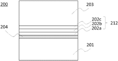
- semiconductor laminate 1 and 2 are diagrams showing one form of the structure of the semiconductor laminate according to the present invention, respectively.
- the semiconductor laminates (hereinafter, may be simply referred to as “semiconductor laminates”) 100 and 200 having a crystalline metal oxide semiconductor film according to the present invention are basically the substrates 101 and 201 and the buffer layer 112. , 212, and the buffer layers 112 and 212 formed on the main surfaces of the substrates 101 and 201, including the crystalline metal oxide semiconductor films 103 and 203, and the crystalline metal oxide further formed on the buffer layers 112 and 212. It is composed of semiconductor films 103 and 203.
- the substrates 101 and 201 are not particularly limited as long as they contain a crystal as a main component, and may be a known substrate. It may be an insulator, a conductor, a semiconductor, a single crystal, or a polycrystal. Further, among the metal elements contained in the substrate, it is preferable to use a substrate in which the main component metal element contained most is aluminum. Above all, it is preferable to use a sapphire wafer from the viewpoint of quality and cost.
- the thicknesses of the substrates 101 and 201 are not particularly limited, but are preferably about 200 to 800 ⁇ m from the viewpoint of cost.
- the area of the main surface of the substrates 101 and 201 is preferably 10 cm 2 or more, and more preferably about 10 cm (4 inches) or more in diameter. If the substrates 101 and 201 have a large diameter in this way, the crystalline metal oxide semiconductor films 103 and 203 formed on the substrates 101 and 201 will have higher quality and higher productivity. In addition, the degree of freedom in device design is increased.
- the shapes of the substrates 101 and 201 are not particularly limited in the present invention.
- the buffer layers 112 and 212 may be formed directly on the substrate 101 as shown in FIG. 1, or may be formed via another layer. As another layer, for example, when a release layer for separating the crystalline metal oxide semiconductor film from the substrate is introduced, it may be formed on the release layer 204 as shown in FIG.
- the buffer layers 112 and 212 are laminated structures of a plurality of buffer films 102a, 102b, 102c, 202a, 202b, and 202c having different compositions, respectively. Each buffer membrane shall have a different composition. More preferably, among the metal elements contained in the crystalline metal oxide semiconductor films 103 and 203 described later, the main component metal element contained most, or the metal element contained in the base of the buffer layers 112 and 212. It is good to contain the most abundant main component metal element. Of course, both the main component metal element of the crystalline metal oxide semiconductor films 103 and 203 and the main component metal element of the base of the buffer layers 112 and 212 may be contained.
- the main component metal element of the base of the buffer layers 112 and 212 refers to the main component metal element of the substrate 101 in the form of FIG. 1 and the main component metal element of the release layer 204 in the form of FIG.
- the buffer layer is composed of three buffer films, but the present invention is not limited to this, and two or more or more (multiple layers) buffer films having different compositions are formed. If so, the number of layers and the composition of the entire buffer film can be appropriately adjusted depending on the conditions such as the thickness of the crystalline metal oxide semiconductor film.
- the film thickness of each of the buffer films having at least two layers among the buffer films having two or more layers (multiple layers) is set to 200 nm or more and 650 nm or less.
- the thicknesses of the buffer films of at least two layers may be the same or different, but a sufficient effect cannot be obtained below 200 nm, and stress becomes remarkable above 650 nm. Warpage and defects will be introduced. It is preferable that all the film thicknesses of the buffer films having two or more layers (multiple layers) are 200 nm or more and 650 nm or less.
- the buffer film contains the main component metal elements of the crystalline metal oxide semiconductor films 103 and 203
- the crystalline metal increases from the substrate 101 and 201 sides toward the crystalline metal oxide semiconductor films 103 and 203. It is preferable to stack the buffer films so that the composition ratio of the main component metal elements of the oxide semiconductor films 103 and 203 is large.
- the buffer film contains the main component metal element of the base of the buffer layers 112 and 212
- the buffer layers 112 and 212 move from the substrates 101 and 201 to the crystalline metal oxide semiconductor films 103 and 203. It is preferable to stack the buffer film so that the composition ratio of the main component metal element of the base is small.
- the buffer film is (Al x Ga 1-x ) 2 O 3 (0 ⁇ . It is preferable to form x ⁇ 1) and reduce the value of x from the buffer film 102a toward the buffer film 102c.
- a substrate in which the main component metal element contained most in the substrate is aluminum, and to use the substrate of the buffer layer as the substrate. It is advantageous in terms of quality and cost.
- the main components of the crystalline metal oxide semiconductor films 103 and 203 are not particularly limited as long as they are crystalline metal oxides having a corundum structure, and for example, aluminum, titanium, vanadium, chromium, iron, gallium, rhodium, indium, and the like.
- the main component can be a crystalline metal oxide containing any of iridium.
- the main component metal element contained in the crystalline metal oxide semiconductor films 103 and 203 the main component metal element contained most preferably is gallium.
- Ga 2 O 3 is particularly preferable. This is because Ga 2 O 3 has a large band gap and can be expected to be applied as various semiconductor devices.
- the three elements selected from the above metal elements are A, B, and C (A x By C 1-x-y ) , 2 O 3 (0 ⁇ x ⁇ 1, 0 ⁇ y ⁇ 1) is shown. It can also be a ternary metal oxide.
- the crystalline metal oxide semiconductor films 103 and 203 may have a single-layer structure of the above-mentioned metal oxide, or may have a laminated structure of a plurality of crystal films having different components such as composition and dopant.
- the film thicknesses of the crystalline metal oxide semiconductor films 103 and 203 are preferably 1 ⁇ m or more, preferably 3 ⁇ m or more. With such a film thickness, the orientation of the crystals is improved, and a higher quality crystalline metal oxide semiconductor film can be obtained.
- the semiconductor laminate according to the present invention may be doped with impurities in order to impart conductivity, depending on the design of the semiconductor element or the like to be applied.
- impurities for example, when the semiconductor films 103 and 203 contain at least gallium, any one of silicon, germanium, tin, magnesium, and copper, or a combination thereof can be preferably used.
- the conductive type is n type.
- the concentration of impurities added by doping depends on the design of the target final product, but is generally 1 ⁇ 10 16 cm -3 or more and 8 ⁇ 10 22 cm -3 or less.
- the crystalline metal oxide semiconductor films 103 and 203 can be laminated with crystals to which impurities are added at different concentrations.
- the buffer layers 102 and 202 may also have conductivity by the same doping.
- semiconductor element Further, by using the semiconductor laminate according to the present invention as described above, it is possible to provide a semiconductor element having at least a buffer layer and a crystalline metal oxide semiconductor film in the semiconductor laminate. Such a semiconductor element may include a substrate or may have the substrate removed.
- the semiconductor device according to the present invention uses a high-quality crystalline metal oxide semiconductor film in which the introduction of crystal defects is reduced and cracks and warpage are suppressed, and is a high-quality semiconductor device.
- An application example (specific example) of the semiconductor element will be described in detail later.
- the method for manufacturing the semiconductor laminate according to the present invention is not particularly limited.
- a semiconductor laminate can be obtained by appropriately selecting a substrate and a buffer layer according to the type of the crystalline metal oxide semiconductor film and the semiconductor element to be applied and forming a film on the substrate.
- the film forming method is not particularly limited, and can be realized by a wide range of known methods such as plasma CVD, LPCVD (decompression CVD), APCVD (atmospheric pressure CVD), mist CVD, HVPE, sputtering, and ion plating.
- a buffer layer is formed on the main surface of the substrate, either directly or via another layer.
- the buffer layer is formed by forming a film so as to include two or more buffer films having different compositions and having a thickness of 200 nm or more and 650 nm or less. It is preferable that all of the plurality of buffer films constituting the buffer layer are formed with a thickness of 200 nm or more and 650 nm or less.
- a crystalline metal oxide semiconductor film having a corundum structure is formed on the buffer layer to obtain a semiconductor laminate according to the present invention. After that, a semiconductor device is manufactured by further forming an electrode on the crystalline metal oxide semiconductor film.
- the semiconductor laminate containing the substrate, the buffer layer, and the crystalline metal oxide semiconductor film can be used as it is, or the substrate can be removed to leave the buffer layer and the crystalline metal oxide semiconductor film, or the substrate. And the buffer layer may be removed to leave only the crystalline metal oxide semiconductor film. In this way, it is possible to manufacture a high-performance semiconductor device using a high-quality crystalline metal oxide semiconductor film in which the introduction of crystal defects is reduced and cracks and warpage are suppressed.
- the semiconductor laminate having the crystalline metal oxide semiconductor film as described above has a reduced defect density and excellent electrical characteristics, and is industrially useful.
- a semiconductor laminate having such a crystalline metal oxide semiconductor film can be suitably used for various semiconductor devices and the like, and is particularly useful for power devices.
- the semiconductor laminate having the crystalline metal oxide semiconductor film according to the present invention includes a horizontal element (horizontal device) in which an electrode is formed on one side of the crystalline metal oxide semiconductor film and a crystalline metal oxide. It can be classified into vertical elements (vertical devices) having electrodes on both the front and back sides of the semiconductor film. In the present invention, it can be suitably used for both horizontal and vertical devices, but it is particularly preferable to use it for vertical devices.
- semiconductor elements include a shot key barrier diode (SBD), a metal semiconductor field effect transistor (MESFET), a high electron mobility transistor (HEMT), a semiconductor field effect transistor (PLC), a junction field effect transistor (JFET), and insulation. Examples thereof include a gate type bipolar transistor (IGBT) or a light emitting diode (LED).
- n-type semiconductor layer n + type semiconductor, n-semiconductor layer, etc.
- another layer for example, an insulator layer or a conductor layer
- an intermediate layer or a buffer layer buffer layer
- FIG. 3 is an example of the SBD according to the present invention.
- the SBD 300 includes an n-type semiconductor layer 301a to which a relatively low concentration of doping has been applied, an n + type semiconductor layer 301b to which a relatively high concentration of doping has been applied, a Schottky electrode 302 and an ohmic electrode 303.
- the material of the Schottky electrode 302 and the ohmic electrode 303 may be known electrode materials, and examples of the electrode material include aluminum, molybdenum, cobalt, zirconium, tin, niobium, iron, chromium, tantalum, and titanium.
- Metals such as gold, platinum, vanadium, manganese, nickel, copper, hafnium, tungsten, iridium, zinc, indium, palladium, neodymium or silver or alloys thereof, tin oxide, zinc oxide, renium oxide, indium oxide, indium tin oxide
- metal oxide conductive films such as (ITO) and indium tin oxide (IZO), organic conductive compounds such as polyaniline, polythiophene or polypyrrole, or mixtures and laminates thereof.
- the Schottky electrode 302 and the ohmic electrode 303 can be formed by a known means such as a vacuum vapor deposition method or a sputtering method. More specifically, for example, when a shotkey electrode is formed by using two kinds of the first metal and the second metal among the metals, it is composed of a layer made of the first metal and a second metal. This can be done by laminating the layers and patterning the layer made of the first metal and the layer made of the second metal by using a photolithography technique.
- the SBD 300 When a reverse bias is applied to the SBD 300, the depletion layer (not shown) spreads in the n-type semiconductor layer 301a, resulting in a high withstand voltage SBD. Further, when a forward bias is applied, electrons flow from the ohmic electrode 303 to the Schottky electrode 302. Therefore, the SBD of the present invention is excellent for high withstand voltage and large current, has a high switching speed, and is also excellent in withstand voltage and reliability.
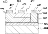
- FIG. 4 is an example of a HEMT according to the present invention.
- the HEMT400 includes an n-type semiconductor layer 401 with a wide bandgap, an n-type semiconductor layer 402 with a narrow bandgap, an n + type semiconductor layer 403, a semi-insulator layer 404, a buffer layer 405, a gate electrode 406, a source electrode 407, and a drain electrode 408. It is equipped with.
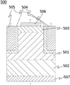
- FIG. 5 is an example of the MOSFET according to the present invention.
- the MOSFET 500 includes an n-type semiconductor layer 501, an n + type semiconductor layers 502 and 503, a gate insulating film 504, a gate electrode 505, a source electrode 506, and a drain electrode 507.
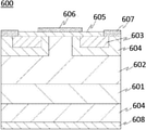
- FIG. 6 is an example of the IGBT according to the present invention.
- the IGBT 600 includes an n-type semiconductor layer 601, an n-type semiconductor layer 602, an n + type semiconductor layer 603, a p-type semiconductor layer 604, a gate insulating film 605, a gate electrode 606, an emitter electrode 607, and a collector electrode 608.
- FIG. 7 is an example of the LED according to the present invention.
- the LED 700 includes a first electrode 701, an n-type semiconductor layer 702, a light emitting layer 703, a p-type semiconductor layer 704, a translucent electrode 705, and a second electrode 706.
- the material of the translucent electrode examples include a conductive material of an oxide containing indium or titanium. More specifically, for example, In 2 O 3 , ZnO, SnO 2 , Ga 2 O 3 , TIO 2 , CeO 2 or a mixed crystal of two or more of these, or those doped with these can be mentioned.
- a translucent electrode can be formed by providing these materials by a known means such as sputtering. Further, after forming the translucent electrode, thermal annealing may be performed for the purpose of making the translucent electrode transparent.
- the materials of the first electrode 701 and the second electrode 706 include, for example, aluminum, molybdenum, cobalt, zirconium, tin, niobium, iron, chromium, tantalum, titanium, gold, platinum, vanadium, manganese, nickel, copper, and the like.
- Metals such as hafnium, tungsten, iridium, zinc, indium, palladium, neodymium or silver or alloys thereof, tin oxide, zinc oxide, renium oxide, indium oxide, indium tin oxide (ITO), indium zinc oxide (IZO) and the like.
- the film forming method of the electrode is not particularly limited, and is a wet method such as a printing method, a spray method, a coating method, a physical method such as a vacuum vapor deposition method, a sputtering method, and an ion plating method, CVD, and plasma CVD. It can be formed on the substrate according to a method appropriately selected in consideration of suitability with the material from chemical methods such as a method.
- Example 1 A semiconductor laminate was produced as follows using a mist CVD apparatus. Two atomizers (atomizer A and atomizer B) and a quartz tubular reactor were prepared, both atomizers were connected by a quartz tube, and a quartz tube was branched from the quartz tube to be connected to the reactor.
- a 4-inch c-plane sapphire substrate with a thickness of 0.6 mm was loaded into the reactor in a state of leaning against a quartz susceptor, and heated so that the substrate temperature became 450 ° C.
- ultrasonic vibration was propagated to the precursors of the atomizers A and B through water by a 2.4 MHz ultrasonic vibrator to mist the precursor.
- the supply of nitrogen gas to the atomizer B is stopped, the flow rate of the nitrogen gas to the atomizer A is 20 L / min, and the mixture of mist and nitrogen gas is supplied to the reactor for 180 minutes to form a semiconductor film having a film thickness of about 7 ⁇ m. did.
- the obtained semiconductor film was confirmed to be ⁇ -Ga 2 O 3 by X-ray diffraction measurement.
- the cracks, warpage, and dislocation density of the prepared film were evaluated.
- the presence or absence of cracks is evaluated as a linear defect with a length of 1 mm or more observed in the bright field of an optical microscope on the entire surface of the substrate, and the warp is the shortest distance between the straight line connecting both ends of the substrate and the concave or convex apex.
- the dislocation density was quantified by the TEM method using a sample in which the vertical cross section of the laminated body was sliced to a thickness of 100 nm.
- Example 2 A semiconductor laminate was produced in the same manner as in Example 1 except that the film thickness of each buffer film was 200 nm (Example 2) and 650 nm (Example 3). The produced semiconductor film was confirmed to be ⁇ -Ga 2 O 3 by X-ray diffraction measurement. After that, the same evaluation as in Example 1 was performed.
- Example 1 A semiconductor laminate was produced in the same manner as in Example 1 except that the film thickness of each buffer film was 150 nm (Comparative Example 1) and 700 nm (Comparative Example 2). The produced semiconductor film was confirmed to be ⁇ -Ga 2 O 3 by X-ray diffraction measurement. After that, the same evaluation as in Example 1 was performed.
- Example 4 A semiconductor laminate was produced in the same manner as in Example 1 except that the film thicknesses of the first and second buffer films were 150 nm. The produced semiconductor film was confirmed to be ⁇ -Ga 2 O 3 by X-ray diffraction measurement. After that, the same evaluation as in Example 1 was performed.
- Example 3 A semiconductor laminate was produced in the same manner as in Example 1 except that the film thicknesses of the buffer films of the first layer, the second layer, and the third layer were set to 150 nm. The produced semiconductor film was confirmed to be ⁇ -Ga 2 O 3 by X-ray diffraction measurement. After that, the same evaluation as in Example 1 was performed.
- Table 1 shows the evaluation results of cracks, warpage, and dislocation densities of Examples 1, 2, and 3 and Comparative Examples 1, 2.
- Table 2 shows the evaluation results of cracks, warpage, and dislocation densities of Example 4 and Comparative Example 3.
- the semiconductor laminate according to the present invention is a high-quality film in which cracks and warpage are suppressed and the dislocation density is reduced. ..
- the semiconductor laminate obtained in the comparative example of the prior art had cracks and significant warpage, and had a high dislocation density.
- the present invention is not limited to the above embodiment.
- the above-described embodiment is an example, and any of the above-described embodiments having substantially the same configuration as the technical idea described in the claims of the present invention and having the same effect and effect is the present invention. Is included in the technical scope of.
Landscapes
- Engineering & Computer Science (AREA)
- Microelectronics & Electronic Packaging (AREA)
- Power Engineering (AREA)
- Chemical & Material Sciences (AREA)
- Computer Hardware Design (AREA)
- Condensed Matter Physics & Semiconductors (AREA)
- General Physics & Mathematics (AREA)
- Physics & Mathematics (AREA)
- Manufacturing & Machinery (AREA)
- Ceramic Engineering (AREA)
- Materials Engineering (AREA)
- Crystallography & Structural Chemistry (AREA)
- Metallurgy (AREA)
- Organic Chemistry (AREA)
- Inorganic Chemistry (AREA)
- Chemical Kinetics & Catalysis (AREA)
- General Chemical & Material Sciences (AREA)
- Mechanical Engineering (AREA)
- Junction Field-Effect Transistors (AREA)
- Crystals, And After-Treatments Of Crystals (AREA)
- Electrodes Of Semiconductors (AREA)
- Recrystallisation Techniques (AREA)
- Liquid Deposition Of Substances Of Which Semiconductor Devices Are Composed (AREA)
- Chemical Vapour Deposition (AREA)
Abstract
本発明は、少なくとも、基体と、バッファ層と、少なくとも1種の金属元素を含みコランダム構造を有する結晶性金属酸化物半導体膜とを含み、前記基体の主表面の上に直接または別の層を介して前記バッファ層を有し、前記バッファ層の上に前記結晶性金属酸化物半導体膜を有する半導体積層体であって、前記バッファ層は、組成がそれぞれ異なる複数のバッファ膜の積層構造体であり、前記複数のバッファ膜のうちの少なくとも2層のバッファ膜の膜厚が、200nm以上650nm以下であることを特徴とする半導体積層体である。これにより、ヘテロエピタキシャル成長により形成される場合であっても、結晶欠陥、反り、及びクラックが抑制された高品質なコランダム型結晶性金属酸化物半導体膜を有する半導体積層体が提供される。
Description
本発明は、半導体積層体、半導体素子および半導体素子の製造方法に関する。
高耐圧、低損失および高耐熱を実現できる次世代のスイッチング素子として、バンドギャップの大きな酸化ガリウム(Ga2O3)を用いた半導体素子が注目されており、インバータなどの電力用半導体装置への適用が期待されている。
特にコランダム型のα-Ga2O3金属酸化物は、比較的安価なサファイア基体を用いたエピタキシャル成長が可能であり、さらにミストCVD(化学気相成長)法(特許文献1)やHVPE(ハイドライド気相成長)法(特許文献2)といった常圧プロセスが適用できることから、既存の電力用半導体素子にくらべて低コストで製造できる期待がある。
一方で、上述のようなヘテロエピタキシャル成長では、基体とエピタキシャル層との格子不整合や熱膨張係数の違いによるストレスに起因して、転位などの結晶欠陥や反りやクラックが生じるという問題があった。特に大面積の基体に成膜を行う場合にはこれらの問題がより顕著になり、その生産が困難であった。
特許文献3では下地基板に2層以上の酸化物層が形成されている下地基板を用いて、300μm四方以上の領域でクラックを含まない膜厚3μm以上のコランダム構造を有するInAlGaO系半導体膜を形成した例が示されている。しかしながら、特許文献3に示されている例によりクラックを抑制できるのは、実際のところ直径4インチ(約10センチメートル)未満の小口径基板に限られ、実用的なサイズ(直径4インチ以上)の基板を用いた場合には効果が不十分であった。また小口径の基板においても、基板の反りを抑制するには至らなかった。
本発明は、上記問題を解決するためになされたものであり、ヘテロエピタキシャル成長により形成される場合であっても、結晶欠陥、反り、及びクラックが抑制された高品質なコランダム型結晶性金属酸化物半導体膜を有する半導体積層体及び高性能な半導体素子を提供することを目的とする。
本発明は、上記目的を達成するためになされたものであり、少なくとも、基体と、バッファ層と、少なくとも1種の金属元素を含みコランダム構造を有する結晶性金属酸化物半導体膜とを含み、前記基体の主表面の上に直接または別の層を介して前記バッファ層を有し、前記バッファ層の上に前記結晶性金属酸化物半導体膜を有する半導体積層体であって、前記バッファ層は、組成がそれぞれ異なる複数のバッファ膜の積層構造体であり、前記複数のバッファ膜のうちの少なくとも2層のバッファ膜の膜厚が、200nm以上650nm以下である半導体積層体を提供する。
本発明は、また、少なくとも、基体と、バッファ層と、少なくとも1種の金属元素を含みコランダム構造を有する結晶性金属酸化物半導体膜とを含み、前記基体の主表面の上に直接または別の層を介して前記バッファ層を有し、前記バッファ層の上に前記結晶性金属酸化物半導体膜を有する半導体積層体であって、前記バッファ層は、組成がそれぞれ異なる複数のバッファ膜の積層構造体であり、前記複数のバッファ膜の膜厚は、すべて200nm以上650nm以下である半導体積層体を提供する。
このようなバッファ層を有することにより、基体と結晶性金属酸化物半導体膜の格子不整合に由来するストレスを効果的に緩和することができるので、結晶欠陥の導入を低減し、さらにクラックと反りが抑制された、高品質な結晶性金属酸化物半導体膜を有する半導体積層体が得られるものとなる。
このとき、前記バッファ膜は、前記結晶性金属酸化物半導体膜に含まれる金属元素のうち、最も多く含まれる主成分金属元素を含むことが好ましい。
さらに、前記バッファ層は、該バッファ層の前記基体側から前記結晶性金属酸化物半導体膜側に向かうにつれて、前記結晶性金属酸化物半導体膜の前記主成分金属元素の組成比が大きくなるように前記複数のバッファ膜が積層した積層構造体であることが好ましい。
これにより、バッファ層のストレス緩和効果をさらに高めることができるので、バッファ層上の結晶性金属酸化物半導体膜がさらに高品質なものとなる。
このとき、前記バッファ膜は、前記バッファ層の下地に含まれる金属元素のうち、最も多く含まれる主成分金属元素を含むことが好ましい。
さらに、前記バッファ層は、該バッファ層の前記基体側から前記結晶性金属酸化物半導体膜側に向かうにつれて、前記バッファ層の下地の前記主成分金属元素の組成比が小さくなるように前記複数のバッファ膜が積層した積層構造体であることが好ましい。
これにより、バッファ層のストレス緩和効果をさらに高めることができるので、バッファ層上の結晶性金属酸化物半導体膜がさらに高品質なものとなる。
このとき、前記バッファ層の下地は前記基体であり、前記基体の前記主成分金属元素はアルミニウムであることが好ましい。
アルミニウムを主成分金属元素とする、例えばサファイアウェハのようなウェハは、品質およびコストの面から基体として好適に用いることができる。
このとき、前記結晶性金属酸化物半導体膜の前記主成分金属元素はガリウムであることが好ましい。
ガリウム酸化膜は、バンドギャップが大きく、本発明に係る結晶性金属酸化物半導体膜として好適に用いることができる。
このとき、前記結晶性金属酸化物半導体膜の膜厚は1μm以上であることが好ましい。
これにより、結晶性金属酸化物半導体膜がより高品質なものとなる。
このとき、前記基体の主表面の面積は10cm2以上であることが好ましい。
これにより、結晶性金属酸化物半導体膜がさらに高品質なものとなる。また、デバイス設計の自由度が高くなる。
このとき、上記に記載の半導体積層体における、少なくとも前記バッファ層と前記結晶性金属酸化物半導体膜を備える半導体素子を提供することが好ましい。
これにより、電気特性の優れた、高性能な半導体素子となる。
また、本発明は、少なくとも結晶性金属酸化物半導体膜と電極とを有する半導体素子の製造方法であって、基体の主表面の上に、バッファ層として、それぞれ異なる組成を有するとともに200nm以上650nm以下の厚さのバッファ膜を2層以上含む、複数層のバッファ膜を形成する工程と、前記バッファ層の上に、コランダム構造を有する結晶性金属酸化物半導体膜を形成する工程と、少なくとも前記結晶性金属酸化物半導体膜の上に電極を形成する工程とを有する半導体素子の製造方法を提供する。
また、本発明は、さらに、少なくとも結晶性金属酸化物半導体膜と電極とを有する半導体素子の製造方法であって、基体の主表面の上に、バッファ層として、それぞれ異なる組成を有するとともに200nm以上650nm以下の厚さのバッファ膜を複数層形成する工程と、前記バッファ層の上に、コランダム構造を有する結晶性金属酸化物半導体膜を形成する工程と、少なくとも前記結晶性金属酸化物半導体膜の上に電極を形成する工程とを有する半導体素子の製造方法を提供する。
このようなバッファ層を形成することにより、基体と結晶性金属酸化物半導体膜の格子不整合に由来するストレスを効果的に緩和することができるので、結晶欠陥の導入が低減され、さらにクラックと反りが抑制された高品質な結晶性金属酸化物半導体膜を用いた、高性能な半導体素子が得られる。
以上のように、本発明によれば、ヘテロエピタキシャル成長により形成される場合であっても、結晶欠陥、反り、及びクラックが抑制された高品質なコランダム型結晶性金属酸化物半導体膜を有する半導体積層体、半導体素子および半導体素子の製造方法を提供することができる。また、本発明に係る結晶性金属酸化物半導体膜を有する半導体積層体を用いることで、高性能な半導体素子を製造することができる。
以下、本発明を詳細に説明するが、本発明はこれらに限定されるものではない。
上述のように、ヘテロエピタキシャル成長により形成される場合であっても、結晶欠陥、反り、及びクラックが抑制された高品質なコランダム型結晶性金属酸化物半導体膜を有する半導体積層体が求められていた。
本発明者は、上記課題について鋭意検討を重ねた結果、少なくとも、基体と、バッファ層と、少なくとも1種の金属元素を含みコランダム構造を有する結晶性金属酸化物半導体膜とを含み、前記基体の主表面の上に直接または別の層を介して前記バッファ層を有し、前記バッファ層の上に前記結晶性金属酸化物半導体膜を有する半導体積層体であって、前記バッファ層は、組成がそれぞれ異なる複数のバッファ膜の積層構造体であり、前記複数のバッファ膜のうちの少なくとも2層のバッファ膜の膜厚が、200nm以上650nm以下である半導体積層体、また、前記バッファ層は、組成がそれぞれ異なる複数のバッファ膜の積層構造体であり、前記複数のバッファ膜の膜厚は、すべて200nm以上650nm以下である半導体積層体により、基体と半導体膜の格子不整合に由来するストレスを効果的に緩和することができるので、結晶欠陥の導入を低減し、さらにクラックと反りが抑制された、高品質な半導体積層体が得られることを見出し、本発明を完成した。
また、本発明者は、少なくとも結晶性金属酸化物半導体膜と電極とを有する半導体素子の製造方法であって、基体の主表面の上に、バッファ層として、それぞれ異なる組成を有するとともに200nm以上650nm以下の厚さのバッファ膜を2層以上含む、複数層のバッファ膜を形成する工程と、前記バッファ層の上に、コランダム構造を有する結晶性金属酸化物半導体膜を形成する工程と、少なくとも前記結晶性金属酸化物半導体膜の上に電極を形成する工程とを有する半導体素子の製造方法、また、基体の主表面の上に、バッファ層として、それぞれ異なる組成を有するとともに200nm以上650nm以下の厚さのバッファ膜を複数層形成する工程と、前記バッファ層の上に、コランダム構造を有する結晶性金属酸化物半導体膜を形成する工程と、少なくとも前記結晶性金属酸化物半導体膜の上に電極を形成する工程とを有する半導体素子の製造方法により、結晶欠陥が低減され、さらにクラックや反りが抑制された、高品質な結晶性金属酸化物半導体膜を用いた半導体素子が得られることを見出し、本発明を完成した。
以下、図面を参照して説明する。
(半導体積層体)
図1、図2はそれぞれ、本発明に係る半導体積層体の構造の一形態を示す図である。本発明に係る結晶性金属酸化物半導体膜を有する半導体積層体(以下、単に「半導体積層体」と呼称する場合もある)100、200は、基本的に、基体101、201と、バッファ層112、212と、結晶性金属酸化物半導体膜103、203とを含み、基体101、201の主表面の上に形成されたバッファ層112、212と、さらにその上に形成された結晶性金属酸化物半導体膜103、203で構成されている。
図1、図2はそれぞれ、本発明に係る半導体積層体の構造の一形態を示す図である。本発明に係る結晶性金属酸化物半導体膜を有する半導体積層体(以下、単に「半導体積層体」と呼称する場合もある)100、200は、基本的に、基体101、201と、バッファ層112、212と、結晶性金属酸化物半導体膜103、203とを含み、基体101、201の主表面の上に形成されたバッファ層112、212と、さらにその上に形成された結晶性金属酸化物半導体膜103、203で構成されている。
(基体)
基体101、201は、結晶物を主成分として含んでいれば特に限定されず、公知の基板であってよい。絶縁体であってもよいし、導電体であってもよいし、半導体であってもよいし、単結晶であってもよいし、多結晶であっても良い。また、基体に含まれる金属元素のうち、最も多く含まれる主成分金属元素がアルミニウムである基体を用いることが好ましい。なかでも、品質およびコストの面から、サファイアウェハを用いるのが好ましい。
基体101、201は、結晶物を主成分として含んでいれば特に限定されず、公知の基板であってよい。絶縁体であってもよいし、導電体であってもよいし、半導体であってもよいし、単結晶であってもよいし、多結晶であっても良い。また、基体に含まれる金属元素のうち、最も多く含まれる主成分金属元素がアルミニウムである基体を用いることが好ましい。なかでも、品質およびコストの面から、サファイアウェハを用いるのが好ましい。
基体の主面の面方位は特に限定されず、サファイアウェハの場合、例えばc面、m面、a面などの主要面が使用できる。また、ジャスト面に対してオフ角を有するものであってもよい。オフ角は、特に限定されないが、好ましくは0°~15°である。
基体101、201の厚さは、特に限定されないが、コストの面から200~800μm程度が好ましい。また、基体101、201の主表面の面積は、10cm2以上であるのが良く、より好ましくは直径約10cm(4インチ)以上であるのが良い。このように基体101、201を大直径のものとすれば、基体101、201の上に形成される結晶性金属酸化物半導体膜103、203がさらに高品質かつ生産性の高いものとなる。また、デバイス設計の自由度が高くなる。基体101、201の形状は、本発明においては特に限定されない。
(バッファ層)
バッファ層112、212は、図1のように基体101上へ直接形成されても良いし、別の層を介して形成されても良い。別の層として、例えば、結晶性金属酸化物半導体膜を基体から分離するための剥離層を導入する場合などでは、図2のように剥離層204上へ形成されていてもよい。
バッファ層112、212は、図1のように基体101上へ直接形成されても良いし、別の層を介して形成されても良い。別の層として、例えば、結晶性金属酸化物半導体膜を基体から分離するための剥離層を導入する場合などでは、図2のように剥離層204上へ形成されていてもよい。
(バッファ膜)
バッファ層112、212は、それぞれ組成の異なる複数のバッファ膜102a、102b、102c、202a、202b、202cの積層構造体となっている。バッファ膜はそれぞれが異なる組成を有するものとする。より好ましくは、後述する結晶性金属酸化物半導体膜103、203に含まれる金属元素のうち、最も多く含まれる主成分金属元素、または、バッファ層112、212の下地に含まれる金属元素のうち、最も多く含まれる主成分金属元素を含んでいるのが良い。もちろん、結晶性金属酸化物半導体膜103、203の主成分金属元素とバッファ層112、212の下地の主成分金属元素の両方を含んでいても良い。ここで、バッファ層112、212の下地の主成分金属元素とは、図1の形態では基体101の主成分金属元素を、また図2の形態では剥離層204の主成分金属元素を指す。
バッファ層112、212は、それぞれ組成の異なる複数のバッファ膜102a、102b、102c、202a、202b、202cの積層構造体となっている。バッファ膜はそれぞれが異なる組成を有するものとする。より好ましくは、後述する結晶性金属酸化物半導体膜103、203に含まれる金属元素のうち、最も多く含まれる主成分金属元素、または、バッファ層112、212の下地に含まれる金属元素のうち、最も多く含まれる主成分金属元素を含んでいるのが良い。もちろん、結晶性金属酸化物半導体膜103、203の主成分金属元素とバッファ層112、212の下地の主成分金属元素の両方を含んでいても良い。ここで、バッファ層112、212の下地の主成分金属元素とは、図1の形態では基体101の主成分金属元素を、また図2の形態では剥離層204の主成分金属元素を指す。
なお、図1および図2の形態では、バッファ層は3層のバッファ膜で構成されているが、本発明はこれに限らず、組成がそれぞれ異なる2層以上(複数層)のバッファ膜が形成されていれば、結晶性金属酸化物半導体膜の厚さなどの条件により、バッファ膜全体の層数および組成を適宜調整することができる。このとき、2層以上(複数層)のバッファ膜のうちの少なくとも2層のバッファ膜のそれぞれの膜厚を200nm以上650nm以下とする。少なくとも2層のバッファ膜の厚さはすべて同じ厚さであっても、異なる厚さであっても良いが、200nm未満では十分な効果が得られず、また650nm超では応力が顕著になって反りと欠陥が導入されるようになる。2層以上(複数層)のバッファ膜のすべての膜厚が200nm以上650nm以下であれば好ましい。
また、バッファ膜が結晶性金属酸化物半導体膜103、203の主成分金属元素を含む場合には、基体101、201側から結晶性金属酸化物半導体膜103、203側に向かうにつれて、結晶性金属酸化物半導体膜103、203の主成分金属元素の組成比が大きくなるようにバッファ膜を積層するのが良い。また、バッファ膜が、バッファ層112、212の下地の主成分金属元素を含む場合には、基体101、201側から結晶性金属酸化物半導体膜103、203側に向かうにつれて、バッファ層112、212の下地の主成分金属元素の組成比が小さくなるようにバッファ膜を積層するのが良い。例えば、図1の形態でAl2O3ウェハ上にα-Ga2O3の結晶性金属酸化物半導体膜を形成する場合、バッファ膜を(AlxGa1-x)2O3(0<x<1)で形成し、xの値をバッファ膜102aからバッファ膜102cに向かって小さくするのが良い。
また、基体に含まれる金属元素のうち、最も多く含まれる主成分金属元素がアルミニウムである基体を用い、バッファ層の下地を基体とすることが好ましい。品質およびコストの面で有利である。
(結晶性金属酸化物半導体膜)
結晶性金属酸化物半導体膜103、203の主成分は、コランダム構造を取る結晶性金属酸化物であれば特に限定されず、例えば、アルミニウム、チタン、バナジウム、クロム、鉄、ガリウム、ロジウム、インジウム、イリジウムのいずれかを含む結晶性金属酸化物を主成分とすることができる。結晶性金属酸化物半導体膜103、203に含まれる金属元素のうち、最も多く含まれる主成分金属元素はガリウムであることがより好ましい。具体的には、Al2O3、Ti2O3、V2O3、Cr2O3、Fe2O3、Ga2O3、Rh2O3、In2O3、Ir2O3であり、本発明においては特にGa2O3であるのが好ましい。Ga2O3は、バンドギャップが大きく、様々な半導体素子としての応用が期待できるからである。また上記の金属元素から選ばれる2元素をA、Bとした場合に(AxB1-x)2O3(0<x<1)で表される2元系の金属酸化物や、あるいは、上記の金属元素から選ばれる3元素をA、B、Cとした場合に(AxByC1-x-y)2O3(0<x<1、0<y<1)で表される3元系の金属酸化物とすることもできる。
結晶性金属酸化物半導体膜103、203の主成分は、コランダム構造を取る結晶性金属酸化物であれば特に限定されず、例えば、アルミニウム、チタン、バナジウム、クロム、鉄、ガリウム、ロジウム、インジウム、イリジウムのいずれかを含む結晶性金属酸化物を主成分とすることができる。結晶性金属酸化物半導体膜103、203に含まれる金属元素のうち、最も多く含まれる主成分金属元素はガリウムであることがより好ましい。具体的には、Al2O3、Ti2O3、V2O3、Cr2O3、Fe2O3、Ga2O3、Rh2O3、In2O3、Ir2O3であり、本発明においては特にGa2O3であるのが好ましい。Ga2O3は、バンドギャップが大きく、様々な半導体素子としての応用が期待できるからである。また上記の金属元素から選ばれる2元素をA、Bとした場合に(AxB1-x)2O3(0<x<1)で表される2元系の金属酸化物や、あるいは、上記の金属元素から選ばれる3元素をA、B、Cとした場合に(AxByC1-x-y)2O3(0<x<1、0<y<1)で表される3元系の金属酸化物とすることもできる。
さらに、結晶性金属酸化物半導体膜103、203は、上記の金属酸化物の単層構造でも良いし、組成やドーパントなどの含有成分が異なる複数の結晶膜の積層構造であっても良い。
結晶性金属酸化物半導体膜103、203の膜厚は1μm以上であるのが良く、好ましくは3μm以上であるのが良い。このような膜厚にすることで結晶の配向性が改善し、より高品質な結晶性金属酸化物半導体膜とすることができる。
また、本発明に係る半導体積層体は、適用する半導体素子等の設計に応じて、導電性を付与すべく不純物でドーピングされていてもよい。この場合の不純物としては、例えば半導体膜103、203が少なくともガリウムを含む場合には、シリコン、ゲルマニウム、スズ、マグネシウム、銅のいずれか、またはこれらの組合せが好適に使用できる。尚、この場合の導電型はn型となる。ドーピングにより添加される不純物の濃度は、目的とする最終製品の設計にもよるが、1×1016cm-3以上8×1022cm-3以下とするのが一般的である。特に結晶性金属酸化物半導体膜103、203は、異なる濃度で不純物が添加された結晶膜の積層とすることができる。またバッファ層102、202も同様のドーピングにより導電性を具備して良い。
(半導体素子)
また、上記したような、本発明に係る半導体積層体を用い、半導体積層体における、少なくともバッファ層と結晶性金属酸化物半導体膜を有する半導体素子を提供することができる。このような半導体素子は、基体を含むものであっても、基体が除去されたものであっても良い。本発明に係る半導体素子は、結晶欠陥の導入が低減され、さらにクラックや反りが抑制された、高品質な結晶性金属酸化物半導体膜を用いるものであり、高品質な半導体素子である。半導体素子の応用例(具体例)については、後で詳しく説明する。
また、上記したような、本発明に係る半導体積層体を用い、半導体積層体における、少なくともバッファ層と結晶性金属酸化物半導体膜を有する半導体素子を提供することができる。このような半導体素子は、基体を含むものであっても、基体が除去されたものであっても良い。本発明に係る半導体素子は、結晶欠陥の導入が低減され、さらにクラックや反りが抑制された、高品質な結晶性金属酸化物半導体膜を用いるものであり、高品質な半導体素子である。半導体素子の応用例(具体例)については、後で詳しく説明する。
(半導体積層体の製造方法)
本発明に係る半導体積層体の製造方法は特に限定されない。結晶性金属酸化物半導体膜の種類や、適用する半導体素子に応じて、基体、バッファ層を適宜選択し、基体上に成膜を行うことで、半導体積層体を得ることができる。成膜方法は特に限定されず、プラズマCVD、LPCVD(減圧CVD)、APCVD(大気圧CVD)、ミストCVD、HVPE、スパッタ、イオンプレーティングなど公知の幅広い手法により実現できる。
本発明に係る半導体積層体の製造方法は特に限定されない。結晶性金属酸化物半導体膜の種類や、適用する半導体素子に応じて、基体、バッファ層を適宜選択し、基体上に成膜を行うことで、半導体積層体を得ることができる。成膜方法は特に限定されず、プラズマCVD、LPCVD(減圧CVD)、APCVD(大気圧CVD)、ミストCVD、HVPE、スパッタ、イオンプレーティングなど公知の幅広い手法により実現できる。
(半導体素子の製造方法)
また、基体の主表面の上に、直接又は別の層を介してバッファ層を形成する。バッファ層は、それぞれ異なる組成を有するとともに200nm以上650nm以下の厚さのバッファ膜を2層以上含むように製膜することにより、形成する。バッファ層を構成する複数層のバッファ膜のすべてを、厚さ200nm以上650nm以下として製膜することが好ましい。このバッファ層の上に、コランダム構造を有する結晶性金属酸化物半導体膜を形成し、本発明に係る半導体積層体を得る。その後に、さらに、結晶性金属酸化物半導体膜の上に電極を形成することで、半導体素子を製造する。このとき、基体と、バッファ層と、結晶性金属酸化物半導体膜を含む半導体積層体をそのまま用いることもできるし、基体を除去してバッファ層と結晶性金属酸化物半導体膜を残したり、基体とバッファ層を除去して、結晶性金属酸化物半導体膜のみを残したりしてもよい。このようにして、結晶欠陥の導入が低減され、さらにクラックや反りが抑制された高品質な結晶性金属酸化物半導体膜を用いた、高性能な半導体素子を製造することができる。
また、基体の主表面の上に、直接又は別の層を介してバッファ層を形成する。バッファ層は、それぞれ異なる組成を有するとともに200nm以上650nm以下の厚さのバッファ膜を2層以上含むように製膜することにより、形成する。バッファ層を構成する複数層のバッファ膜のすべてを、厚さ200nm以上650nm以下として製膜することが好ましい。このバッファ層の上に、コランダム構造を有する結晶性金属酸化物半導体膜を形成し、本発明に係る半導体積層体を得る。その後に、さらに、結晶性金属酸化物半導体膜の上に電極を形成することで、半導体素子を製造する。このとき、基体と、バッファ層と、結晶性金属酸化物半導体膜を含む半導体積層体をそのまま用いることもできるし、基体を除去してバッファ層と結晶性金属酸化物半導体膜を残したり、基体とバッファ層を除去して、結晶性金属酸化物半導体膜のみを残したりしてもよい。このようにして、結晶欠陥の導入が低減され、さらにクラックや反りが抑制された高品質な結晶性金属酸化物半導体膜を用いた、高性能な半導体素子を製造することができる。
(応用できる半導体素子の例)
上記のような結晶性金属酸化物半導体膜を有する半導体積層体は、欠陥密度が低減され、電気特性に優れており、工業的に有用なものである。このような結晶性金属酸化物半導体膜を有する半導体積層体は、様々な半導体素子等に好適に用いることができ、とりわけ、パワーデバイスに有用である。
上記のような結晶性金属酸化物半導体膜を有する半導体積層体は、欠陥密度が低減され、電気特性に優れており、工業的に有用なものである。このような結晶性金属酸化物半導体膜を有する半導体積層体は、様々な半導体素子等に好適に用いることができ、とりわけ、パワーデバイスに有用である。
また、本発明に係る結晶性金属酸化物半導体膜を有する半導体積層体は、電極が結晶性金属酸化物半導体膜の片面側に形成された横型の素子(横型デバイス)と、結晶性金属酸化物半導体膜の表裏両面側にそれぞれ電極を有する縦型の素子(縦型デバイス)に分類することができる。本発明においては、横型デバイスにも縦型デバイスにも好適に用いることができるが、中でも、縦型デバイスに用いることが好ましい。半導体素子としては、例えば、ショットキーバリアダイオード(SBD)、金属半導体電界効果トランジスタ(MESFET)、高電子移動度トランジスタ(HEMT)、半導体電界効果トランジスタ(MOSFET)、接合電界効果トランジスタ(JFET)、絶縁ゲート型バイポーラトランジスタ(IGBT)または発光ダイオード(LED)などが挙げられる。
以下、本発明の結晶性金属酸化物半導体膜をn型半導体層(n+型半導体やn-半導体層等)に適用した場合の好適な例を、図面を用いて説明するが、本発明は、これらの例に限定されるものではない。なお、以下に例示する半導体素子において、さらに他の層(例えば絶縁体層や導体層)などが含まれていてもよいし、また、中間層や緩衝層(バッファ層)などは適宜省いてもよい。
図3は、本発明に係るSBDの一例である。SBD300は、相対的に低濃度のドーピングを施したn-型半導体層301a、相対的に高濃度のドーピングを施したn+型半導体層301b、ショットキー電極302およびオーミック電極303を備えている。
ショットキー電極302およびオーミック電極303の材料は、公知の電極材料であってもよく、前記電極材料としては、例えば、アルミニウム、モリブデン、コバルト、ジルコニウム、スズ、ニオブ、鉄、クロム、タンタル、チタン、金、プラチナ、バナジウム、マンガン、ニッケル、銅、ハフニウム、タングステン、イリジウム、亜鉛、インジウム、パラジウム、ネオジムもしくは銀等の金属またはこれらの合金、酸化錫、酸化亜鉛、酸化レニウム、酸化インジウム、酸化インジウム錫(ITO)、酸化亜鉛インジウム(IZO)等の金属酸化物導電膜、ポリアニリン、ポリチオフェン又はポリピロ-ルなどの有機導電性化合物、またはこれらの混合物並びに積層体などが挙げられる。
ショットキー電極302およびオーミック電極303の形成は、例えば、真空蒸着法またはスパッタリング法などの公知の手段により行うことができる。より具体的には、例えば、前記金属のうち2種類の第1の金属と第2の金属とを用いてショットキー電極を形成する場合、第1の金属からなる層と第2の金属からなる層を積層させ、第1の金属からなる層および第2の金属からなる層に対して、フォトリソグラフィの手法を利用したパターニングを施すことにより行うことができる。
SBD300に逆バイアスが印加された場合には、空乏層(図示せず)がn-型半導体層301aの中に広がるため、高耐圧のSBDとなる。また、順バイアスが印加された場合には、オーミック電極303からショットキー電極302へ電子が流れる。したがって、本発明のSBDは、高耐圧・大電流用に優れており、スイッチング速度も速く、耐圧性・信頼性にも優れている。
図4は、本発明に係るHEMTの一例である。HEMT400は、バンドギャップの広いn型半導体層401、バンドギャップの狭いn型半導体層402、n+型半導体層403、半絶縁体層404、緩衝層405、ゲート電極406、ソース電極407およびドレイン電極408を備えている。
図5は、本発明に係るMOSFETの一例である。MOSFET500はn-型半導体層501、n+型半導体層502及び503、ゲート絶縁膜504、ゲート電極505、ソース電極506およびドレイン電極507を備えている。
図6は、本発明に係るIGBTの一例である。IGBT600は、n型半導体層601、n-型半導体層602、n+型半導体層603、p型半導体層604、ゲート絶縁膜605、ゲート電極606、エミッタ電極607およびコレクタ電極608を備えている。
図7は、本発明に係るLEDの一例である。LED700は、第1の電極701、n型半導体層702、発光層703、p型半導体層704、透光性電極705、第2の電極706を備えている。
透光性電極の材料としては、インジウムまたはチタンを含む酸化物の導電性材料などが挙げられる。より具体的には、例えば、In2O3、ZnO、SnO2、Ga2O3、TiO2、CeO2またはこれらの2以上の混晶またはこれらにドーピングされたものなどが挙げられる。これらの材料を、スパッタリング等の公知の手段で設けることによって、透光性電極を形成できる。また、透光性電極を形成した後に、透光性電極の透明化を目的とした熱アニールを施してもよい。
第1の電極701及び第2の電極706の材料としては、例えば、アルミニウム、モリブデン、コバルト、ジルコニウム、スズ、ニオブ、鉄、クロム、タンタル、チタン、金、プラチナ、バナジウム、マンガン、ニッケル、銅、ハフニウム、タングステン、イリジウム、亜鉛、インジウム、パラジウム、ネオジムもしくは銀等の金属またはこれらの合金、酸化錫、酸化亜鉛、酸化レニウム、酸化インジウム、酸化インジウム錫(ITO)、酸化亜鉛インジウム(IZO)等の金属酸化物導電膜、ポリアニリン、ポリチオフェン又はポリピロ-ルなどの有機導電性化合物、またはこれらの混合物などが挙げられる。電極の製膜法は特に限定されることはなく、印刷方式、スプレー法、コ-ティング方式等の湿式方式、真空蒸着法、スパッタリング法、イオンプレ-ティング法等の物理的方式、CVD、プラズマCVD法等の化学的方式、などの中から前記材料との適性を考慮して適宜選択した方法に従って前記基板上に形成することができる。
以下、実施例を挙げて本発明について具体的に説明するが、これは本発明を限定するものではない。
(実施例1)
ミストCVD装置を用いて、以下のように半導体積層体を作製した。2台の噴霧器(噴霧器A、噴霧器B)と石英製の管状反応炉を用意し、両噴霧器を石英管で接続し、さらにそこから石英管を枝出しして反応器と接続した。
ミストCVD装置を用いて、以下のように半導体積層体を作製した。2台の噴霧器(噴霧器A、噴霧器B)と石英製の管状反応炉を用意し、両噴霧器を石英管で接続し、さらにそこから石英管を枝出しして反応器と接続した。
次に、ガリウムアセチルアセトナート0.04mol/Lの水溶液に濃度34%の塩酸を体積比で1%加え、スターラーで60分間攪拌し、前駆体を得た。この前駆体を噴霧器Aに充填した。次に、アルミニウムアセチルアセトナート0.06mol/Lの水溶液に濃度34%の塩酸を体積比で1%加え、スターラーで60分間攪拌し、前駆体を得た。この前駆体を噴霧器Bに充填した。
次に、厚さ0.6mmの4インチc面サファイア基板を石英製サセプターに立てかけた状態で反応炉に装填し、基板温度が450℃になるように加温した。次に、2.4MHzの超音波振動子により水を通じて噴霧器A、Bの前駆体に超音波振動を伝播させて、前駆体をミスト化した。
この後、噴霧器Aと噴霧器Bに総流量として毎分20Lの窒素ガスを加え、ミストと窒素ガスの混合気を反応炉に供給し、基板の上に膜厚400nmのバッファ膜を一層形成した。続けて、噴霧器Bへの窒素ガス流量を減少させることで混合気中のAl比率を低下させながら、同様の成膜を3回繰り返して2層目から4層目のバッファ膜を積層した。各バッファ膜中のAl/Ga比率は、1層目から4層目にかけて、0.60、0.30、0.15、0.05とした。次に、噴霧器Bへの窒素ガス供給を止め、噴霧器Aへの窒素ガス流量を毎分20Lとしてミストと窒素ガスの混合気を反応器に180分間供給し、膜厚約7μmの半導体膜を形成した。
次に、窒素ガス供給と基板への加温を停止し、室温付近まで冷却してから基板を反応炉から取り出した。得られた半導体膜は、X線回折測定により、α-Ga2O3であることが確認された。
この後、作製した膜について、クラック、反りおよび転位密度を評価した。クラックは、基板全面の光学顕微鏡明視野で観察される1mm長以上の直線状欠陥として、発生の有無を評価し、また反りは基板の両端を結ぶ直線と凹または凸の頂点との最短の距離として評価した。また転位密度は、積層体の縦断面を100nm厚の薄片化した試料を使い、TEM法によって定量した。
(実施例2、3)
各バッファ膜の膜厚を200nm(実施例2)、650nm(実施例3)としたこと以外は実施例1と同様に半導体積層体を作製した。作製した半導体膜は、X線回折測定により、α-Ga2O3であることが確認された。この後、実施例1と同様の評価を行った。
各バッファ膜の膜厚を200nm(実施例2)、650nm(実施例3)としたこと以外は実施例1と同様に半導体積層体を作製した。作製した半導体膜は、X線回折測定により、α-Ga2O3であることが確認された。この後、実施例1と同様の評価を行った。
(比較例1、2)
各バッファ膜の膜厚を150nm(比較例1)、700nm(比較例2)としたこと以外は実施例1と同様に半導体積層体を作製した。作製した半導体膜は、X線回折測定により、α-Ga2O3であることが確認された。この後、実施例1と同様の評価を行った。
各バッファ膜の膜厚を150nm(比較例1)、700nm(比較例2)としたこと以外は実施例1と同様に半導体積層体を作製した。作製した半導体膜は、X線回折測定により、α-Ga2O3であることが確認された。この後、実施例1と同様の評価を行った。
(実施例4)
1層目と2層目のバッファ膜の膜厚を150nmとしたこと以外は実施例1と同様に半導体積層体を作製した。作製した半導体膜は、X線回折測定により、α-Ga2O3であることが確認された。この後、実施例1と同様の評価を行った。
1層目と2層目のバッファ膜の膜厚を150nmとしたこと以外は実施例1と同様に半導体積層体を作製した。作製した半導体膜は、X線回折測定により、α-Ga2O3であることが確認された。この後、実施例1と同様の評価を行った。
(比較例3)
1層目、2層目および3層目のバッファ膜の膜厚を150nmとしたこと以外は実施例1と同様に半導体積層体を作製した。作製した半導体膜は、X線回折測定により、α-Ga2O3であることが確認された。この後、実施例1と同様の評価を行った。
1層目、2層目および3層目のバッファ膜の膜厚を150nmとしたこと以外は実施例1と同様に半導体積層体を作製した。作製した半導体膜は、X線回折測定により、α-Ga2O3であることが確認された。この後、実施例1と同様の評価を行った。
実施例1、2、3および比較例1、2のクラック、反り、転位密度の評価結果を表1に示す。また、実施例4および比較例3のクラック、反り、転位密度の評価結果を表2に示す。


表1および表2に示した実施例の結果で示されるように、本発明に係る半導体積層体は、クラックと反りが抑制され、かつ転位密度が低減された高品質な膜であることが分かる。一方、従来技術の比較例で得られた半導体積層体は、クラックと著しい反りが生じ、また転位密度も高かった。
なお、本発明は、上記実施形態に限定されるものではない。上記実施形態は例示であり、本発明の特許請求の範囲に記載された技術的思想と実質的に同一な構成を有し、同様な作用効果を奏するものは、いかなるものであっても本発明の技術的範囲に包含される。
Claims (13)
- 少なくとも、基体と、バッファ層と、少なくとも1種の金属元素を含みコランダム構造を有する結晶性金属酸化物半導体膜とを含み、
前記基体の主表面の上に直接または別の層を介して前記バッファ層を有し、前記バッファ層の上に前記結晶性金属酸化物半導体膜を有する半導体積層体であって、
前記バッファ層は、組成がそれぞれ異なる複数のバッファ膜の積層構造体であり、
前記複数のバッファ膜のうちの少なくとも2層のバッファ膜の膜厚が、200nm以上650nm以下であることを特徴とする半導体積層体。 - 少なくとも、基体と、バッファ層と、少なくとも1種の金属元素を含みコランダム構造を有する結晶性金属酸化物半導体膜とを含み、
前記基体の主表面の上に直接または別の層を介して前記バッファ層を有し、前記バッファ層の上に前記結晶性金属酸化物半導体膜を有する半導体積層体であって、
前記バッファ層は、組成がそれぞれ異なる複数のバッファ膜の積層構造体であり、
前記複数のバッファ膜の膜厚は、すべて200nm以上650nm以下であることを特徴とする半導体積層体。 - 前記バッファ膜は、前記結晶性金属酸化物半導体膜に含まれる金属元素のうち、最も多く含まれる主成分金属元素を含むことを特徴とする請求項1又は2に記載の半導体積層体。
- 前記バッファ層は、該バッファ層の前記基体側から前記結晶性金属酸化物半導体膜側に向かうにつれて、前記結晶性金属酸化物半導体膜の前記主成分金属元素の組成比が大きくなるように前記複数のバッファ膜が積層した積層構造体であることを特徴とする請求項3に記載の半導体積層体。
- 前記バッファ膜は、前記バッファ層の下地に含まれる金属元素のうち、最も多く含まれる主成分金属元素を含むことを特徴とする請求項3又は請求項4のいずれか一項に記載の半導体積層体。
- 前記バッファ層は、該バッファ層の前記基体側から前記結晶性金属酸化物半導体膜側に向かうにつれて、前記バッファ層の下地の前記主成分金属元素の組成比が小さくなるように前記複数のバッファ膜が積層した積層構造体であることを特徴とする請求項5に記載の半導体積層体。
- 前記バッファ層の下地は前記基体であり、前記基体の前記主成分金属元素はアルミニウムであることを特徴とする請求項5又は請求項6のいずれか一項に記載の半導体積層体。
- 前記結晶性金属酸化物半導体膜の前記主成分金属元素はガリウムであることを特徴とする請求項3から請求項7のいずれか一項に記載の半導体積層体。
- 前記結晶性金属酸化物半導体膜の膜厚は1μm以上であることを特徴とする請求項1から請求項8のいずれか一項に記載の半導体積層体。
- 前記基体の主表面の面積は10cm2以上であることを特徴とする請求項1から請求項9のいずれか一項に記載の半導体積層体。
- 請求項1から10のいずれかに記載の半導体積層体における、少なくとも前記バッファ層と前記結晶性金属酸化物半導体膜を備えることを特徴とする半導体素子。
- 少なくとも結晶性金属酸化物半導体膜と電極とを有する半導体素子の製造方法であって、
基体の主表面の上に、バッファ層として、それぞれ異なる組成を有するとともに200nm以上650nm以下の厚さのバッファ膜を2層以上含む、複数層のバッファ膜を形成する工程と、
前記バッファ層の上に、コランダム構造を有する結晶性金属酸化物半導体膜を形成する工程と、
少なくとも前記結晶性金属酸化物半導体膜の上に電極を形成する工程とを有することを特徴とする半導体素子の製造方法。 - 少なくとも結晶性金属酸化物半導体膜と電極とを有する半導体素子の製造方法であって、
基体の主表面の上に、バッファ層として、それぞれ異なる組成を有するとともに200nm以上650nm以下の厚さのバッファ膜を複数層形成する工程と、
前記バッファ層の上に、コランダム構造を有する結晶性金属酸化物半導体膜を形成する工程と、
少なくとも前記結晶性金属酸化物半導体膜の上に電極を形成する工程とを有することを特徴とする半導体素子の製造方法。
Priority Applications (4)
| Application Number | Priority Date | Filing Date | Title |
|---|---|---|---|
| EP21854515.0A EP4194592A4 (en) | 2020-08-06 | 2021-06-18 | SEMICONDUCTOR LAMINATE, SEMICONDUCTOR ELEMENT, AND METHOD FOR PRODUCING SEMICONDUCTOR ELEMENT |
| US18/018,913 US20230245883A1 (en) | 2020-08-06 | 2021-06-18 | Semiconductor laminate, semiconductor device, and method for manufacturing semiconductor device |
| CN202180057772.7A CN116157550A (zh) | 2020-08-06 | 2021-06-18 | 半导体层叠体、半导体元件及半导体元件的制造方法 |
| KR1020237003593A KR20230048008A (ko) | 2020-08-06 | 2021-06-18 | 반도체 적층체, 반도체 소자 및 반도체 소자의 제조방법 |
Applications Claiming Priority (4)
| Application Number | Priority Date | Filing Date | Title |
|---|---|---|---|
| JP2020-133535 | 2020-08-06 | ||
| JP2020133535 | 2020-08-06 | ||
| JP2021-043094 | 2021-03-17 | ||
| JP2021043094A JP7061214B2 (ja) | 2020-08-06 | 2021-03-17 | 半導体積層体、半導体素子および半導体素子の製造方法 |
Publications (1)
| Publication Number | Publication Date |
|---|---|
| WO2022030114A1 true WO2022030114A1 (ja) | 2022-02-10 |
Family
ID=80119644
Family Applications (1)
| Application Number | Title | Priority Date | Filing Date |
|---|---|---|---|
| PCT/JP2021/023252 WO2022030114A1 (ja) | 2020-08-06 | 2021-06-18 | 半導体積層体、半導体素子および半導体素子の製造方法 |
Country Status (6)
| Country | Link |
|---|---|
| US (1) | US20230245883A1 (ja) |
| EP (1) | EP4194592A4 (ja) |
| JP (2) | JP7346626B2 (ja) |
| KR (1) | KR20230048008A (ja) |
| CN (1) | CN116157550A (ja) |
| WO (1) | WO2022030114A1 (ja) |
Citations (6)
| Publication number | Priority date | Publication date | Assignee | Title |
|---|---|---|---|---|
| JP2013028480A (ja) | 2011-07-27 | 2013-02-07 | Kochi Univ Of Technology | ドーパントを添加した結晶性の高い導電性α型酸化ガリウム薄膜およびその生成方法 |
| JP2014072533A (ja) * | 2013-10-10 | 2014-04-21 | Roca Kk | 半導体装置 |
| JP2018002544A (ja) | 2016-06-30 | 2018-01-11 | 株式会社Flosfia | 結晶性酸化物半導体膜およびその製造方法 |
| JP2019033142A (ja) * | 2017-08-04 | 2019-02-28 | 高知県公立大学法人 | 深紫外発光素子およびその製造方法 |
| JP2019034882A (ja) | 2017-08-21 | 2019-03-07 | 株式会社Flosfia | 結晶膜の製造方法 |
| CN110504343A (zh) * | 2018-05-18 | 2019-11-26 | 中国科学院苏州纳米技术与纳米仿生研究所 | 基于蓝宝石衬底的氧化镓薄膜及其生长方法和应用 |
Family Cites Families (8)
| Publication number | Priority date | Publication date | Assignee | Title |
|---|---|---|---|---|
| JP2008091470A (ja) * | 2006-09-29 | 2008-04-17 | Showa Denko Kk | Iii族窒化物化合物半導体積層構造体の成膜方法 |
| JP2009021540A (ja) * | 2007-06-13 | 2009-01-29 | Rohm Co Ltd | ZnO系薄膜及びZnO系半導体素子 |
| EP2807670A1 (de) * | 2012-01-27 | 2014-12-03 | Merck Patent GmbH | Verfahren zur herstellung elektrisch halbleitender oder leitender schichten mit verbesserter leitfähigkeit |
| KR102098250B1 (ko) * | 2013-10-21 | 2020-04-08 | 삼성전자 주식회사 | 반도체 버퍼 구조체, 이를 포함하는 반도체 소자 및 반도체 버퍼 구조체를 이용한 반도체 소자 제조방법 |
| US9806125B2 (en) * | 2015-07-28 | 2017-10-31 | Carrier Corporation | Compositionally graded photodetectors |
| JP2020001997A (ja) * | 2017-08-21 | 2020-01-09 | 株式会社Flosfia | 結晶膜の製造方法 |
| JP2019034883A (ja) * | 2017-08-21 | 2019-03-07 | 株式会社Flosfia | 結晶膜の製造方法 |
| JP6909191B2 (ja) * | 2018-09-27 | 2021-07-28 | 信越化学工業株式会社 | 積層体、半導体装置及び積層体の製造方法 |
-
2021
- 2021-06-18 EP EP21854515.0A patent/EP4194592A4/en active Pending
- 2021-06-18 US US18/018,913 patent/US20230245883A1/en active Pending
- 2021-06-18 CN CN202180057772.7A patent/CN116157550A/zh active Pending
- 2021-06-18 WO PCT/JP2021/023252 patent/WO2022030114A1/ja active Application Filing
- 2021-06-18 KR KR1020237003593A patent/KR20230048008A/ko active Search and Examination
-
2022
- 2022-02-16 JP JP2022021858A patent/JP7346626B2/ja active Active
-
2023
- 2023-09-06 JP JP2023144667A patent/JP2023169231A/ja active Pending
Patent Citations (6)
| Publication number | Priority date | Publication date | Assignee | Title |
|---|---|---|---|---|
| JP2013028480A (ja) | 2011-07-27 | 2013-02-07 | Kochi Univ Of Technology | ドーパントを添加した結晶性の高い導電性α型酸化ガリウム薄膜およびその生成方法 |
| JP2014072533A (ja) * | 2013-10-10 | 2014-04-21 | Roca Kk | 半導体装置 |
| JP2018002544A (ja) | 2016-06-30 | 2018-01-11 | 株式会社Flosfia | 結晶性酸化物半導体膜およびその製造方法 |
| JP2019033142A (ja) * | 2017-08-04 | 2019-02-28 | 高知県公立大学法人 | 深紫外発光素子およびその製造方法 |
| JP2019034882A (ja) | 2017-08-21 | 2019-03-07 | 株式会社Flosfia | 結晶膜の製造方法 |
| CN110504343A (zh) * | 2018-05-18 | 2019-11-26 | 中国科学院苏州纳米技术与纳米仿生研究所 | 基于蓝宝石衬底的氧化镓薄膜及其生长方法和应用 |
Non-Patent Citations (2)
| Title |
|---|
| RIENA JINNO, TAKAYUKI UCHIDA, KENTARO KANEKO, SHIZUO FUJITA: "Reduction in edge dislocation density in corundum-structured α-Ga 2 O 3 layers on sapphire substrates with quasi-graded α-(Al,Ga) 2 O 3 buffer layers", APPLIED PHYSICS EXPRESS, JAPAN SOCIETY OF APPLIED PHYSICS; JP, JP, vol. 9, no. 7, 1 July 2016 (2016-07-01), JP , pages 071101, XP055758843, ISSN: 1882-0778, DOI: 10.7567/APEX.9.071101 * |
| See also references of EP4194592A4 |
Also Published As
| Publication number | Publication date |
|---|---|
| JP7346626B2 (ja) | 2023-09-19 |
| JP2022070975A (ja) | 2022-05-13 |
| CN116157550A (zh) | 2023-05-23 |
| KR20230048008A (ko) | 2023-04-10 |
| EP4194592A4 (en) | 2024-08-21 |
| US20230245883A1 (en) | 2023-08-03 |
| EP4194592A1 (en) | 2023-06-14 |
| JP2023169231A (ja) | 2023-11-29 |
Similar Documents
| Publication | Publication Date | Title |
|---|---|---|
| JP7352226B2 (ja) | 結晶性半導体膜および半導体装置 | |
| TWI564937B (zh) | A crystalline laminated structure, and a semiconductor device | |
| KR102171509B1 (ko) | n형 질화알루미늄 단결정 기판 및 수직형 질화물 반도체 디바이스 | |
| JP6904517B2 (ja) | 結晶性酸化物半導体膜およびその製造方法 | |
| JP7220257B2 (ja) | 積層体、半導体装置、ミストcvd装置及び成膜方法 | |
| JP6230196B2 (ja) | 結晶性半導体膜および半導体装置 | |
| JP7061214B2 (ja) | 半導体積層体、半導体素子および半導体素子の製造方法 | |
| WO2022030114A1 (ja) | 半導体積層体、半導体素子および半導体素子の製造方法 | |
| KR102721047B1 (ko) | 적층체, 반도체장치 및 적층체의 제조방법 |
Legal Events
| Date | Code | Title | Description |
|---|---|---|---|
| 121 | Ep: the epo has been informed by wipo that ep was designated in this application |
Ref document number: 21854515 Country of ref document: EP Kind code of ref document: A1 |
|
| WWE | Wipo information: entry into national phase |
Ref document number: 2021854515 Country of ref document: EP |
|
| NENP | Non-entry into the national phase |
Ref country code: DE |