WO2022025009A1 - フォトニック結晶素子 - Google Patents
フォトニック結晶素子 Download PDFInfo
- Publication number
- WO2022025009A1 WO2022025009A1 PCT/JP2021/027594 JP2021027594W WO2022025009A1 WO 2022025009 A1 WO2022025009 A1 WO 2022025009A1 JP 2021027594 W JP2021027594 W JP 2021027594W WO 2022025009 A1 WO2022025009 A1 WO 2022025009A1
- Authority
- WO
- WIPO (PCT)
- Prior art keywords
- photonic crystal
- substrate
- crystal element
- waveguide
- element according
- Prior art date
- Legal status (The legal status is an assumption and is not a legal conclusion. Google has not performed a legal analysis and makes no representation as to the accuracy of the status listed.)
- Ceased
Links
Images





Classifications
-
- G—PHYSICS
- G02—OPTICS
- G02F—OPTICAL DEVICES OR ARRANGEMENTS FOR THE CONTROL OF LIGHT BY MODIFICATION OF THE OPTICAL PROPERTIES OF THE MEDIA OF THE ELEMENTS INVOLVED THEREIN; NON-LINEAR OPTICS; FREQUENCY-CHANGING OF LIGHT; OPTICAL LOGIC ELEMENTS; OPTICAL ANALOGUE/DIGITAL CONVERTERS
- G02F1/00—Devices or arrangements for the control of the intensity, colour, phase, polarisation or direction of light arriving from an independent light source, e.g. switching, gating or modulating; Non-linear optics
- G02F1/01—Devices or arrangements for the control of the intensity, colour, phase, polarisation or direction of light arriving from an independent light source, e.g. switching, gating or modulating; Non-linear optics for the control of the intensity, phase, polarisation or colour
- G02F1/21—Devices or arrangements for the control of the intensity, colour, phase, polarisation or direction of light arriving from an independent light source, e.g. switching, gating or modulating; Non-linear optics for the control of the intensity, phase, polarisation or colour by interference
- G02F1/225—Devices or arrangements for the control of the intensity, colour, phase, polarisation or direction of light arriving from an independent light source, e.g. switching, gating or modulating; Non-linear optics for the control of the intensity, phase, polarisation or colour by interference in an optical waveguide structure
- G02F1/2257—Devices or arrangements for the control of the intensity, colour, phase, polarisation or direction of light arriving from an independent light source, e.g. switching, gating or modulating; Non-linear optics for the control of the intensity, phase, polarisation or colour by interference in an optical waveguide structure the optical waveguides being made of semiconducting material
-
- G—PHYSICS
- G02—OPTICS
- G02B—OPTICAL ELEMENTS, SYSTEMS OR APPARATUS
- G02B6/00—Light guides; Structural details of arrangements comprising light guides and other optical elements, e.g. couplings
- G02B6/10—Light guides; Structural details of arrangements comprising light guides and other optical elements, e.g. couplings of the optical waveguide type
- G02B6/12—Light guides; Structural details of arrangements comprising light guides and other optical elements, e.g. couplings of the optical waveguide type of the integrated circuit kind
- G02B6/122—Basic optical elements, e.g. light-guiding paths
- G02B6/1225—Basic optical elements, e.g. light-guiding paths comprising photonic band-gap structures or photonic lattices
-
- G—PHYSICS
- G02—OPTICS
- G02F—OPTICAL DEVICES OR ARRANGEMENTS FOR THE CONTROL OF LIGHT BY MODIFICATION OF THE OPTICAL PROPERTIES OF THE MEDIA OF THE ELEMENTS INVOLVED THEREIN; NON-LINEAR OPTICS; FREQUENCY-CHANGING OF LIGHT; OPTICAL LOGIC ELEMENTS; OPTICAL ANALOGUE/DIGITAL CONVERTERS
- G02F1/00—Devices or arrangements for the control of the intensity, colour, phase, polarisation or direction of light arriving from an independent light source, e.g. switching, gating or modulating; Non-linear optics
- G02F1/01—Devices or arrangements for the control of the intensity, colour, phase, polarisation or direction of light arriving from an independent light source, e.g. switching, gating or modulating; Non-linear optics for the control of the intensity, phase, polarisation or colour
- G02F1/015—Devices or arrangements for the control of the intensity, colour, phase, polarisation or direction of light arriving from an independent light source, e.g. switching, gating or modulating; Non-linear optics for the control of the intensity, phase, polarisation or colour based on semiconductor elements having potential barriers, e.g. having a PN or PIN junction
- G02F1/025—Devices or arrangements for the control of the intensity, colour, phase, polarisation or direction of light arriving from an independent light source, e.g. switching, gating or modulating; Non-linear optics for the control of the intensity, phase, polarisation or colour based on semiconductor elements having potential barriers, e.g. having a PN or PIN junction in an optical waveguide structure
-
- H—ELECTRICITY
- H01—ELECTRIC ELEMENTS
- H01P—WAVEGUIDES; RESONATORS, LINES, OR OTHER DEVICES OF THE WAVEGUIDE TYPE
- H01P1/00—Auxiliary devices
- H01P1/20—Frequency-selective devices, e.g. filters
-
- H—ELECTRICITY
- H01—ELECTRIC ELEMENTS
- H01Q—ANTENNAS, i.e. RADIO AERIALS
- H01Q15/00—Devices for reflection, refraction, diffraction or polarisation of waves radiated from an antenna, e.g. quasi-optical devices
- H01Q15/14—Reflecting surfaces; Equivalent structures
-
- G—PHYSICS
- G02—OPTICS
- G02F—OPTICAL DEVICES OR ARRANGEMENTS FOR THE CONTROL OF LIGHT BY MODIFICATION OF THE OPTICAL PROPERTIES OF THE MEDIA OF THE ELEMENTS INVOLVED THEREIN; NON-LINEAR OPTICS; FREQUENCY-CHANGING OF LIGHT; OPTICAL LOGIC ELEMENTS; OPTICAL ANALOGUE/DIGITAL CONVERTERS
- G02F2202/00—Materials and properties
- G02F2202/32—Photonic crystals
Definitions
- the present invention relates to a photonic crystal element.
- Photonic crystal elements are expected to be applied and developed in a wide range of fields such as optical waveguides, next-generation high-speed communications, sensors, laser processing, and photovoltaic power generation.
- a photonic crystal element is being developed as a waveguide for millimeter waves to terahertz waves, which is the key to next-generation high-speed communication.
- Patent Document 1 a technique using a two-dimensional photonic crystal slab made of a semiconductor material has been proposed.
- the photonic crystal element by such a technique has a relatively large dielectric constant, a large delay of an electric signal, a large propagation loss in a waveguide, and a large variation in characteristics depending on the direction and polarization. There's a problem.
- a main object of the present invention is to provide a photonic crystal device having a small delay of an electric signal, a small propagation loss, and uniform characteristics over the entire device.
- the photonic crystal element according to the embodiment of the present invention has a two-dimensional photonic crystal slab in which pores are periodically formed in a substrate made of a ceramic material, and waves an electromagnetic wave having a frequency of 30 GHz or more and 20 THz or less. ..
- the photonic crystal element is provided at the bottom of the substrate and has a support substrate that supports the substrate; a joint that integrates the substrate and the support substrate; and a lower surface of the substrate. And a cavity defined by the top surface of the support substrate and the junction;
- the ceramic material is polycrystalline or amorphous.
- the porosity of the substrate having a pore size of 1 ⁇ m or more is 0.5 ppm to 3000 ppm.
- the period of the pores is 10 ⁇ m to 1 mm.
- the dielectric constant of the substrate at 100 GHz to 10 THz is 3.6 to 11.5.
- the dielectric loss of the substrate is 0.01 or less.
- the resistivity of the substrate is 100 k ⁇ ⁇ cm or more.
- the ceramic material is one selected from the group consisting of quartz, aluminum nitride, aluminum oxide, silicon carbide, magnesium oxide, and spinel.
- a waveguide is defined in a portion of the substrate in which the pores are not formed, and the waveguide transmits an electromagnetic wave having a frequency of 30 GHz or more and 20 THz or less. do.
- the photonic crystal element can be used as an antenna, a bandpass filter, a coupler, a delay line or an isolator.
- the photonic crystal element is an active element provided in the lower part of the substrate and capable of transmitting, receiving, and amplifying at least one of a support substrate that supports the substrate and electromagnetic waves. It is provided with an active element supported by the support substrate.
- the photonic crystal element comprises a first waveguide of line defects defined in a portion of the substrate where no pores are formed, and the active element and the first in an electromagnetic wave propagation path. It is located between the first waveguide and has a second waveguide capable of waveguideing electromagnetic waves.
- the photonic crystal element is formed in a waveguide of line defects defined in a portion where the pores are not formed in the substrate and a portion in which the pores are not formed in the substrate. It is a defined resonator and includes a resonator located between the active element and the waveguide in the propagation path of the electromagnetic wave and capable of guiding the electromagnetic wave.
- the substrate and the support substrate are directly bonded.
- the support substrate has a recess
- the photonic crystal element comprises a cavity defined by a lower surface of the substrate and a recess of the support substrate.
- the photonic crystal element is a cavity defined by an insulating layer located between the substrate and the supporting substrate, a lower surface of the substrate, an upper surface of the supporting substrate, and the insulating layer. And have.
- the ceramic material by forming a predetermined pore pattern on the substrate of the ceramic material, it is possible to realize a photonic crystal element having a small delay of an electric signal and a small propagation loss.
- the ceramic material by making the ceramic material polycrystalline or amorphous, it is possible to realize a photonic crystal device having uniform properties over the entire device in addition to the above-mentioned excellent properties.
- FIG. 3 is a cross-sectional view taken along the line AA'of the photonic crystal element of FIG.
- FIG. 3 is a cross-sectional view taken along the line BB'of the photonic crystal element of FIG.
- FIG. 6 is a cross-sectional view taken along the line AA'of the photonic crystal element of FIG.
- FIG. 11 (a) and 11 (b) are plan views of two different unit cells included in the photonic crystal element of FIG. 9, and FIG. 11 (a) shows a first unit cell, FIG. 11 (B) shows the second unit cell.
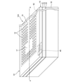
- FIG. 1 is a schematic perspective view of a photonic crystal element according to one embodiment of the present invention.
- the photonic crystal element 100 of the illustrated example has a two-dimensional photonic crystal slab in which pores 12 are periodically formed in a substrate 10 made of a ceramic material.
- a photonic crystal is a multidimensional periodic structure in which a medium having a large refractive index and a medium having a small refractive index are composed of a medium having a period similar to that of light or electromagnetic waves, and has a band structure of light or electromagnetic waves similar to an electron band structure. Have. Therefore, by appropriately designing the periodic structure, a predetermined light or electromagnetic wave forbidden band (photonic band gap) can be expressed.
- a photonic crystal having a forbidden band functions as an object that is neither reflected nor transmitted to light or electromagnetic waves of a predetermined wavelength.
- a line defect is introduced into a photonic crystal having a photonic bandgap, a waveguide mode is formed in the frequency domain of the bandgap, and a waveguide that propagates light or electromagnetic waves with low loss can be realized.
- the photonic crystal element according to the embodiment of the present invention can typically function as a waveguide that guides millimeter waves to terahertz waves.
- the millimeter wave is typically an electromagnetic wave having a frequency of about 30 GHz to 300 GHz; and the terahertz wave is typically an electromagnetic wave having a frequency of about 300 GHz to 20 THz.
- the "photonic crystal element” includes both a wafer on which at least one photonic element is formed (photonic crystal wafer) and a chip obtained by cutting the photonic crystal wafer.
- the photonic crystal in the illustrated example has a two-dimensional photonic crystal slab as described above.
- a two-dimensional photonic crystal slab is a thin plate that uses a dielectric (typically a ceramic material) and is thinned to the wavelength level of electromagnetic waves, and is a material with a refractive index lower than the refractive index of the material that constitutes this thin plate.
- It is a photonic crystal in which the constructed low refractive index portion is provided at an appropriate two-dimensional periodic interval according to the purpose and a desired photonic band gap.
- the pores 12 function as a low refractive index portion
- the portion 14 between the pores 12 and 12 of the substrate 10 functions as a high refractive index portion.
- a portion of the substrate 10 in which the periodic pattern of the holes 12 is not formed becomes a line defect, and the portion of the line defect constitutes the waveguide 16.
- an upper clad and a lower clad having a refractive index lower than that of the thin plate slab may be provided above and below the thin plate slab.
- the upper and lower external environments (air portions) of the photonic crystal element 100 function as the upper clad and the lower clad.
- the substrate 10 is made of a ceramic material as described above. Since the ceramic material that can be used in the embodiment of the present invention has a small dielectric constant (real part) and a small dielectric constant (imaginary part), it is possible to reduce the delay and loss of the electric signal propagating in the photonic crystal. can. Further, the propagation loss in the waveguide can be reduced.
- the substrate is composed of a sintered body of a ceramic material (eg, ceramic powder). Since the sintered body is polycrystalline, the anisotropy in the substrate can be reduced, and therefore the position-dependent characteristics in the photonic crystal element due to the anisotropy (typically, dielectric).
- the ceramic material is preferably polycrystalline or amorphous, more preferably amorphous. Since amorphous can suppress scattering due to grain boundaries peculiar to polycrystals, anisotropy can be further reduced, and the effect of using a ceramic material can be further remarkable.
- a polycrystalline or amorphous ceramic material for example, the complex term (indicating a loss) of the permittivity at a frequency of 0.5 THz or less can be reduced and the variation thereof can be reduced.
- the complex permittivity can be measured by using, for example, terahertz time region spectroscopy.
- semiconductors have been used in many cases as materials constituting photonic crystals. This is because it is easy to form a pore pattern by using a semiconductor process such as photolithography and etching.
- the semiconductor material has a large dielectric constant, the delay of the electric signal propagating in the photonic crystal is large.
- the semiconductor material is a single crystal and has a large anisotropy, and the variation in characteristics (typically, the dielectric constant) depending on the direction in which the electromagnetic wave propagates in the photonic crystal element and the polarization is large.
- ceramic materials particularly sintered bodies have the advantages of low dielectric constant and anisotropy, but are chemically stable and difficult to etch, and are extremely hard and unsuitable for machining.
- the present inventors have holes suitable as a waveguide for millimeter wave to terahertz wave in a sintered body of a ceramic material. It was possible to form a pattern and apply a sintered body of ceramic material to a photonic crystal. The method of forming a photonic crystal will be described later.
- the dielectric constant of the substrate (substantially a ceramic material) at 100 GHz to 10 THz is preferably 3.6 to 11.5, preferably 3.7 when used for an antenna, a bandpass filter, a line, or the like. It is about 10.0, more preferably 3.8 to 9.0. If the dielectric constant is too small, the desired photonic band gap may not be sufficiently formed in the millimeter-wave to terahertz-wave waveguide. If the permittivity is too large, the delay of the electric signal propagating through the photonic crystal may increase.
- the resistivity of the substrate is preferably 100 k ⁇ ⁇ cm or more, more preferably 300 k ⁇ ⁇ cm or more, still more preferably 500 k ⁇ ⁇ cm or more, and particularly preferably 700 k ⁇ ⁇ cm or more. That is all.
- the resistivity is in such a range, the electromagnetic wave can propagate in the material with low loss without affecting the electron conduction.
- this phenomenon is not clear in detail, it can be inferred that if the resistivity is small, the electromagnetic wave is combined with the electron and the energy of the electromagnetic wave is taken away by the electron conduction, resulting in a loss. From this point of view, the larger the resistivity, the more preferable.
- the resistivity can be, for example, 3000 k ⁇ (3 M ⁇ ) ⁇ cm or less.
- the dielectric loss (tan ⁇ ) of the substrate is preferably 0.01 or less, more preferably 0.008 or less, still more preferably 0.006 or less at the frequency used. , Particularly preferably 0.004 or less. If the dielectric loss is in such a range, the propagation loss in the waveguide can be reduced. The smaller the dielectric loss, the more preferable.
- the dielectric loss can be, for example, 0.001 or more.
- the bending strength of the substrate is preferably 50 MPa or more, more preferably 60 MPa or more. If the bending strength is within such a range, the photonic crystal element can be configured as a single layer of the substrate and is not easily deformed. It can be realized. The larger the bending strength, the more preferable. The bending strength can be, for example, 700 MPa or less.
- the coefficient of thermal expansion (linear expansion coefficient) of the substrate is preferably 10 ⁇ 10 -6 / K or less, and more preferably 8 ⁇ 10 -6 / K or less.
- thermal deformation typically, warpage
- a photonic crystal element that can stand on its own as a single layer of the substrate, has sufficient mechanical strength, and has a small change in characteristics is realized by a synergistic effect with the above-mentioned effect of bending strength. be able to.
- the substrate can be made of any suitable ceramic material as long as the above properties can be achieved.
- the ceramic material include quartz, aluminum nitride (AlN), aluminum oxide (Al 2 O 3 ), silicon carbide (SiC), magnesium oxide (Mg O), and spinel (Mg Al 2 O 4 ).
- the thickness of the substrate is preferably 10 ⁇ m to 1 mm, more preferably 0.2 mm to 0.8 mm. When the thickness is within such a range, a photonic crystal element that can stand on its own as a single layer of a substrate and has sufficient mechanical strength can be realized. Further, the propagation loss in the waveguide can be reduced.
- the substrate 10 is periodically formed with holes 12.
- any suitable shape can be adopted as long as a desired photonic band gap can be formed in the waveguide of millimeter wave to terahertz wave.
- Specific examples of the shape of the pores include a substantially spherical shape, an elliptical spherical shape, a substantially cylindrical shape, a polygonal columnar shape (for example, a triangle, a quadrangle, a pentagon, a hexagon, and an octagon in a plan view), and an indeterminate shape.
- the vacancies may be through holes, and for example, a plurality of substantially spherical vacancies may communicate with each other.
- the size of the pores is preferably 10 ⁇ m to 0.8 mm, more preferably 50 ⁇ m to 0.6 mm, and even more preferably 70 ⁇ m to 0.4 mm. If the pore size is in such a range, it is possible to make a photonic band appear in the millimeter wave band and the terahertz wave band. Further, even if a periodic pore structure is formed, a stable photonic crystal element can be realized from the viewpoints of both mechanical strength and long-term reliability.
- the porosity of the substrate is preferably 0.5 ppm to 3000 ppm, more preferably 0.5 ppm to 1000 ppm, and further preferably 0.5 ppm to 100 ppm for pores having a pore size of 1 ⁇ m or more. If the porosity is within such a range, densification is possible, and further, due to the synergistic effect with the above-mentioned effect of setting the pore size within a predetermined range, even if a periodic pore structure is formed, the mechanical strength and long-term reliability are achieved.
- a stable photonic crystal device can be realized from any viewpoint of sex.
- the shape of the pores can be made uniform without variation, the wavelength-dependent characteristics of the transmittance due to the photonic band become clear, and the hand band can be widened. .. If the porosity exceeds 3000 ppm, the propagation loss in the waveguide may increase. It is difficult to make the porosity less than 0.5 ppm by the technique using a sintered body of a ceramic material.
- the “pores” mean bubbles (micropores) possessed by the substrate (ceramic material) itself, and are different from the pores formed to form a photonic crystal.
- the size of the pores or pores is the diameter when the pores or pores are substantially spherical, the diameter when viewed in a plan view when the pores are substantially cylindrical, and the diameter when the pores have other shapes.
- the presence or absence of pores or pores can be confirmed by, for example, an optical CT (Computed Tomography) or a transmittance measuring device.
- the size of the pores or pores can be measured, for example, by a scanning electron microscope (SEM). Since the pores are relatively large in size, they can also be measured with a stereomicroscope or a laser shape measuring instrument.
- the pores 12 can be formed as a periodic pattern as described above.
- the holes 12 are typically arranged to form a regular grid.
- any suitable form can be adopted as long as a desired photonic band gap can be realized in the waveguide of millimeter wave to terahertz wave. Typical examples include a triangular lattice and a square lattice.
- the grid pattern of the pores can be appropriately set according to the purpose and the desired photonic band gap.
- the pores having a diameter d form a square grid with a period P.
- the square lattice pattern is formed on both sides of the photonic crystal element, and the waveguide 16 is formed in the central portion where the lattice pattern is not formed.
- the width of the waveguide 16 can be, for example, 1.01P to 3P (2P in the illustrated example) with respect to the pore period P.
- the number of rows of vacancies in the direction of the waveguide (hereinafter, may be referred to as grid rows) can be 3 to 10 rows (5 rows in the illustrated example) on each side of the waveguide.
- the pore period P may satisfy, for example, the following relationship.
- ⁇ is the wavelength (nm) of light or electromagnetic wave introduced into the waveguide
- n is the refractive index of the substrate. Since the refractive index ⁇ r is proportional to the 1/2 power of the dielectric constant, “n” in the above equation may be replaced with “( ⁇ r) 1/2 ”.
- the pore period P is preferably 10 ⁇ m to 1 mm, more preferably 0.2 mm to 0.8 mm. In one embodiment, the pore period P can be comparable to the thickness of the sintered body (substrate).
- the diameter d of the pores is preferably 0.1P to 0.9P, more preferably 0.2P to 0.6P, with respect to the pore period P.
- the width of the grid pattern is preferably 10P or more, and more preferably 12P to 20P.
- the width of the grid pattern is the distance between the outermost grid pattern in the grid pattern on one side of the waveguide and the outermost grid row in the grid pattern on the other side of the waveguide. Therefore, as shown in the illustrated example, the width of the grid pattern on one side of the waveguide is 4P or more.
- the waveguide 16 has a band shape (straight line shape), but by changing the lattice pattern, it is possible to form a waveguide having a predetermined shape (hence, a predetermined waveguide direction).
- the waveguide may extend in a direction (oblique direction) having a predetermined angle with respect to the long side direction or the short side direction of the photonic crystal element, or may bend at a predetermined point (waveguide direction). May change at a given point).
- the two-dimensional photonic crystal slab can be made by near-net molding of a powder sintering method (substantially, slurry casting molding).
- a powder sintering method substantially, slurry casting molding
- near-net molding of a powder sintering method substantially, slurry casting molding
- the two-dimensional photonic crystal slab may be formed by machining a wafer.
- the protrusions can form pores in the resulting sintered body. Therefore, the shape, size, and the like of the protrusions can be designed according to the shape, size, and the like of the pores formed in the obtained sintered body. In one embodiment, the protrusions can form through holes.
- a slurry containing a ceramic material powder and a predetermined dispersant and a dispersion medium is poured into the molding die.
- the dispersant can be appropriately selected depending on the ceramic material.
- the dispersant is typically an organic compound, more specifically a resin.
- the dispersion medium may be an aqueous system or an organic solvent system. Examples of the aqueous dispersion medium include water and water-soluble alcohol. Examples of the organic solvent-based dispersion medium include paraffin, toluene, and petroleum ether.
- the slurry is prepared, for example, by mixing a ceramic material powder, a dispersant, a dispersion medium and, if necessary, other components (eg, additives). Examples of the mixing means include a ball mill pot, a homogenizer, and a disperser.
- a sintered body (substrate: two-dimensional photonic crystal slab) of a ceramic material having a predetermined pore pattern can be obtained.
- Firing to obtain a sintered body typically includes a calcining step and, if necessary, a calcination step performed before the calcining step.
- the calcination temperature is preferably 1000 ° C. or higher and lower than 1250 ° C., and more preferably 1000 ° C. to 1200 ° C. When the calcination temperature is in such a range, a sintered body having excellent transparency can be obtained.
- the firing temperature is preferably 1500 ° C to 1700 ° C.
- the rate of temperature rise during firing is preferably 20 ° C./min or higher at 1000 ° C. or higher, preferably 20 ° C./min or higher at 1200 ° C. or higher, and more preferably 25 ° C./min or higher.
- degreasing is performed prior to firing.
- the degreasing temperature is preferably 300 ° C to 800 ° C.
- the above-mentioned temporary baking may also serve as degreasing. Degreasing at 1200 ° C. or lower can suppress the precipitation of the crystalline phase.
- a desired sintered body (substrate) can be obtained.
- a desired sintered body (substrate) can be obtained.
- a predetermined pore pattern can be easily applied to the sintered body of a ceramic material. Moreover, it can be formed at low cost. As a result, a photonic crystal device having a small delay of an electric signal, a small propagation loss, and uniform characteristics over the entire device can be obtained easily and at low cost.
- the frequency suitable for the photonic crystal element manufactured by such a method is preferably 125 / ⁇ GHz to 15000 / ⁇ GHz, where the relative permittivity of the substrate material is ⁇ .
- the photonic crystal element 101 of the illustrated example includes a support substrate 30 provided under the substrate 10 and supporting the substrate 10, a joint portion 20 for integrating the substrate 10 and the support substrate 30, and a lower surface and a support of the substrate 10. It further has a cavity 80 defined by an upper surface of the substrate 30 and a joint 20.
- any suitable configuration may be adopted for the support substrate 30.
- the materials constituting the support substrate 30 include silicon (Si), glass, Sialon (Si 3 N 4 -Al 2 O 3 ), and Murite ( 3 Al 2 O 3.2SiO 2 , 2Al 2 O 3.3SiO 2 ). ), Aluminum nitride (AlN), Silicon nitride (Si 3N 4 ) , Magnesium oxide (MgO), Aluminum oxide (Al 2 O 3 ), Spinel (Mg Al 2 O 4 ), Sapphire, Quartz, Crystal, Gallium nitride (GaN) ), Silicon carbide (SiC), gallium oxide (Ga 2 O 3 ).
- Such a material can be integrated with a semiconductor circuit such as an amplifier or a mixer when used at the front end of a millimeter wave to a terahertz wave (for example, as an antenna substrate).
- the coefficient of linear expansion of the material constituting the support substrate 30 is preferably closer to the coefficient of linear expansion of the material constituting the substrate 10. With such a configuration, thermal deformation (typically, warpage) of the photonic crystal element can be suppressed.
- the coefficient of linear expansion of the material constituting the support substrate 30 is in the range of 50% to 150% with respect to the coefficient of linear expansion of the material constituting the substrate 10. From this point of view, the support substrate may be made of the same material as the substrate 10.
- the joint portion 20 is interposed between the substrate 10 and the support substrate 30 to integrate them.
- the joint 20 is configured as the rest of the etching in forming the cavity 80.
- the joint portion 20 typically integrates the substrate 10 and the support substrate 30 by directly joining the upper layer and the lower layer. By integrating the substrate 10 and the support substrate 30 by direct bonding, peeling in the photonic crystal element can be satisfactorily suppressed.
- direct bonding means that two layers or substrates (here, an upper layer and a lower layer) are bonded without the intervention of an adhesive.
- the form of direct bonding can be appropriately set depending on the configuration of the layers or substrates to be bonded to each other.
- direct joining can be realized by the following procedure. In a high vacuum chamber (for example, about 1 ⁇ 10 -6 Pa), a neutralized beam is irradiated to the respective joint surfaces of the upper layer and the lower layer. As a result, each joint surface is activated. Then, in a vacuum atmosphere, the activated joining surfaces are brought into contact with each other and joined at room temperature.
- the load at the time of this joining can be, for example, 100N to 20000N.
- an inert gas is introduced into the chamber, and a high voltage is applied from a DC power source to the electrodes arranged in the chamber.
- a high voltage is applied from a DC power source to the electrodes arranged in the chamber.
- electrons move due to the electric field generated between the electrode (positive electrode) and the chamber (negative electrode), and a beam of atoms and ions due to the inert gas is generated.
- the ion beam is neutralized by the grid, so that the beam of neutral atoms is emitted from the high-speed atomic beam source.
- the atomic species constituting the beam is preferably an inert gas element (for example, argon (Ar), nitrogen (N)).
- the voltage at the time of activation by beam irradiation is, for example, 0.5 kV to 2.0 kV, and the current is, for example, 50 mA to 200 mA.
- the direct bonding method is not limited to this, and FAB (Fast Atom Beam), a surface activation method using an ion gun, an atomic diffusion method, a plasma bonding method, and the like can also be applied. Any suitable configuration may be adopted for the upper layer and the lower layer, respectively, depending on the purpose.
- the cavity 80 is formed by removing the upper layer and the lower layer by etching as described above, and can function as a lower clad.
- the width of the cavity is preferably larger than the width of the optical waveguide.
- the photonic crystal element according to the embodiment of the present invention is used for, for example, an antenna, a bandpass filter, a coupler, a delay line (phase detector), or an isolator. Since these can be realized without using metal wiring, it is possible to suppress conductor loss due to the skin effect and radiation loss due to scattering.
- the photonic crystal device is an active device capable of transmitting, receiving, and amplifying at least one of electromagnetic waves having a frequency of 30 GHz or more and 20 THz or less. Therefore, an active element supported by the support substrate may be provided. In such a photonic crystal element, the active element and the line substrate can be integrated to enable a wafer process, so that variation in characteristics can be reduced and the productivity of the photonic crystal element can be improved. Therefore, an inexpensive photonic crystal element can be realized.
- a configuration is configured in which an electromagnetic wave can be propagated between the waveguide of line defects formed in a two-dimensional photonic crystal slab and the active element.
- the photonic crystal element 102 shown in FIGS. 3 to 5 is formed between the first waveguide of the line defect formed in the two-dimensional photonic crystal slab and the active element and the first waveguide in the electromagnetic wave propagation path. It is located and has a second waveguide (typically a coplanar waveguide in the illustrated example) capable of waveguideing electromagnetic waves.
- the second waveguide is capable of waveguideing an electromagnetic wave transmitted from an active element into the first waveguide.
- the photonic crystal element 102 includes a two-dimensional photonic crystal slab 90 in which pores 12 are periodically formed in a ceramic material substrate 10, and a support provided below the substrate 10 to support the substrate 10. It includes a substrate 30, an active element 40 supported by the support substrate 30, and a coplanar type electrode pattern 50.
- the two-dimensional photonic crystal slab 90 has a photonic crystal portion 90a in which pores 12 are periodically formed in the substrate 10 and a portion in which the pores 12 are not formed in the photonic crystal portion 90a (substrate 10). It includes a defined line defect waveguide 16 and other portions 90b other than the photonic crystal portion 90a. The other portion 90b is typically not formed with a hole 12.
- the support substrate 30 has a recess 31.
- the recess 31 is recessed downward from the upper surface of the support substrate 30.
- the recess 31 is typically open toward one of the waveguide directions of the waveguide 16.
- the lower surface of the ceramic material substrate 10 and the recess 31 of the support substrate 30 define a cavity 81.
- the photonic crystal element 102 includes the cavity 81.
- the cavity 81 is a low dielectric constant portion and functions as a lower clad. Since the photonic crystal element is provided with a cavity, it is possible to stably suppress the leakage of electromagnetic waves propagating in the waveguide from the waveguide.
- the cavity 81 typically overlaps the waveguide 16 in the thickness direction of the substrate 10, and the width of the cavity 81 (dimensions in the direction orthogonal to the waveguide direction of the waveguide 16) is larger than the width of the waveguide 16. big.
- the cavity 81 preferably extends from the optical waveguide 16 to at least a third grid row. Electromagnetic waves not only propagate in the waveguide, but part of the electromagnetic waves may diffuse to the grid array near the waveguide. Therefore, by providing a cavity directly under such a grid array, propagation loss is suppressed. be able to. From this point of view, it is more preferable that the cavity 81 extends from the waveguide 16 to the fifth row, and it is particularly preferable that the cavity 81 extends so as to overlap the entire area of the photonic crystal portion 90a as shown in the illustrated example.
- the ceramic material substrate 10 two-dimensional photonic crystal slab 90
- the support substrate 30 are directly bonded by a bonding portion 20.
- the joint portion 20 is interposed between the other portion 90b of the two-dimensional photonic crystal slab 90 and the portion other than the recess 31 of the support substrate 30 to integrate the substrate 10 and the support substrate 30. do.
- the active element 40 is supported by the support substrate 30, and is typically embedded in a portion of the upper surface of the support substrate 30 other than the recess 31.
- Examples of the active element 40 include a resonance tunnel diode, a Schottky barrier diode, a CMOS transceiver, and an InPHEMT.
- the active element 40 is a resonant tunneling diode.
- the active element 40 can transmit (generate / radiate) electromagnetic waves.
- the active element 40 includes a first element electrode 41 and two second element electrodes 42. Each of the first element electrode 41 and the two second element electrodes 42 extends in the waveguide direction of the waveguide 16.
- the two second element electrodes 42 are arranged so as to be spaced apart from each other in a direction orthogonal to the waveguide direction of the waveguide 16.
- the first element electrode 41 is arranged between the two second element electrodes 42.
- the coplanar type electrode pattern 50 is arranged on a portion (that is, other portions 90b) other than the photonic crystal portion 90a in the ceramic material substrate 10.
- the coplanar electrode pattern 50 and the other portion 90b located below the coplanar electrode pattern 50 constitute a coplanar waveguide as an example of the second waveguide.
- the coplanar type electrode pattern 50 is aligned with the waveguide 16 in the waveguide direction.
- the coplanar type electrode pattern 50 includes a signal electrode 51 extending in the waveguide direction of the waveguide 16 and a plan-view U-shaped ground electrode 52 opened toward the waveguide 16.
- the signal electrode 51 is arranged inside the ground electrode 52, and is arranged at a distance from the ground electrode 52.
- the signal electrode 51 is electrically connected to the first element electrode 41 of the active element 40 via the via 43.
- the ground electrode 52 is electrically connected to the second element electrode 42 of the active element 40 via two vias 44.
- the second waveguide is not limited to the coplanar waveguide, and may be configured as, for example, a microstrip waveguide or a waveguide integrated waveguide.
- the propagation of electromagnetic waves in the photonic crystal element 102 will be described.
- a voltage is applied to the coplanar type electrode pattern 50, an electric field is generated between the signal electrode 51 and the ground electrode 52.
- the active element 40 transmits an electromagnetic wave.
- the electromagnetic wave transmitted from the active element 40 propagates toward the signal electrode 51 via the via 43, and then combines with the electric field formed between the signal electrode 51 and the ground electrode 52 to pass through the substrate 10. It propagates toward the waveguide 16 of the line defect.
- the electromagnetic wave transmitted from the active element 40 is first propagated to the coplanar waveguide.
- the electromagnetic wave is then propagated from the coplanar waveguide to the line defect waveguide 16 and then to the line defect waveguide 16.
- the photonic crystal element 103 shown in FIGS. 6 to 8 is a waveguide 16 having a line defect formed in the two-dimensional photonic crystal slab and a resonator 17 formed in the two-dimensional photonic crystal slab.
- a resonator 17 located between the active element 40 and the waveguide 16 in the propagation path of the electromagnetic wave and capable of guiding the electromagnetic wave is provided.
- the resonator is capable of waveguideing an electromagnetic wave transmitted from an active element into a waveguide.
- the two-dimensional photonic crystal slab 91 included in the photonic crystal element 103 has a line defect waveguide 16 defined as a portion in which the pores 12 are not formed, and a portion in which the pores 12 are not formed.
- a defined mode gap closed type resonator 17 is provided.
- the resonator 17 can receive the electromagnetic wave transmitted from the active element 40, and can send the received electromagnetic wave to the waveguide 16.
- the resonator 17 is aligned with the waveguide 16 in the waveguide direction of the waveguide 16 and is continuous with the waveguide 16.
- the width of the resonator 17 (dimension in the direction orthogonal to the waveguide direction of the waveguide 16) is larger than the width of the waveguide 16.
- the resonator 17 is formed by being surrounded by a row of three rows of holes.
- the photonic crystal element 103 includes an insulating layer 23 located between the ceramic material substrate 10 (two-dimensional photonic crystal slab 91) and the support substrate 30.
- the material of the insulating layer 23 include the above-mentioned ceramic materials, and preferably quartz glass.
- the ceramic material substrate 10 two-dimensional photonic crystal slab 90
- the insulating layer 23 are directly bonded by the bonding portion 21, and the support substrate 30 and the insulating layer 23 are directly bonded by the bonding portion 22. It is joined.
- the joint portion 21 is interposed between the substrate 10 and the insulating layer 23 to integrate the substrate 10 and the insulating layer 23.
- the joint portion 22 is interposed between the insulating layer 23 and the support substrate 30 to integrate the insulating layer 23 and the support substrate 30.
- the insulating layer 23 in the illustrated example has a U-shape in a plan view that is open toward one of the waveguide directions of the waveguide 16.
- the lower surface of the ceramic material substrate 10, the upper surface of the support substrate 30, and the insulating layer 23 define a cavity 82.
- the cavity 82 may be defined by a lower surface of the substrate 10, a joint 22 located on the upper surface of the support substrate 30, and an insulating layer 23.
- the photonic crystal element 103 includes the cavity 82.
- the cavity 82 typically overlaps the waveguide 16 and the resonator 17 in the thickness direction of the substrate 10, and the width of the cavity 82 (dimensions in the direction orthogonal to the waveguide direction of the waveguide 16) is the resonator. It is larger than the width of 17.
- the cavity 82 preferably extends from each of the waveguide 16 and the resonator 17 to the third row of grids and overlaps the entire pore-forming portion of the two-dimensional photonic crystal slab 91, as shown in the illustrated example. It is particularly preferable that it extends like this.
- the propagation of electromagnetic waves in the photonic crystal element 103 will be described.
- the first element electrode 41 functions as an antenna, and electromagnetic waves are transmitted from the first element electrode 41 toward the resonator 17.
- the electromagnetic wave that has reached the resonator 17 is received by the resonator 17 and then sent out from the resonator 17 to the waveguide 16 via a continuous portion between the resonator 17 and the waveguide 16. After that, the electromagnetic wave is propagated in the waveguide 16.
- 3 to 8 show an example in which the active element functions to transmit (generate / radiate) an electromagnetic wave, and the electromagnetic wave transmitted from the active element is coupled to a line defect waveguide via a second waveguide or a resonator.
- the active element functions to receive the electromagnetic wave, and the electromagnetic wave waveguideed through the line defect waveguide is coupled to the active element via the second waveguide or the resonator. Is easily assumed.
- the two-dimensional photonic crystal slab included in the photonic crystal element of the present invention is not limited to the two-dimensional photonic crystal slab including the waveguide of the line defect described above.
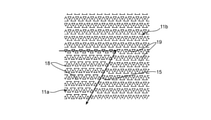
- the two-dimensional photonic crystal slab may be a valley photonic crystal layer 11 in which the boundary of a region composed of two different unit cells functions as a waveguide.
- the valley photonic crystal layer 11 includes a first region 11a composed of a plurality of first unit cells 18 and a second region 11b composed of a plurality of second unit cells 19.
- the first region 11a and the second region 11b are adjacent to each other, and the boundary portion between the first region 11a and the second region 11b is configured as the waveguide 15.
- Each of the first unit cell 18 and the second unit cell 19 is formed with two types of pores having different sizes periodically formed on the ceramic material substrate 10.
- the vacancies are typically arranged to form a regular grid.
- any suitable form can be adopted as long as a desired photonic band gap can be realized in the waveguide of millimeter wave to terahertz wave.
- first unit cell 18 and the second unit cell 19 of the illustrated example three relatively large first holes 12a and three relatively small second holes 12b are formed as a honeycomb lattice (hexagonal lattice). Is arranged to form a honeycomb. In each unit cell, the first holes 12a and the second holes 12b are arranged alternately.
- the first unit cell 18 and the second unit cell 19 have a 180 ° rotational symmetry (line symmetry) relationship. The first unit cell 18 coincides with the second unit cell 19 when rotated by 180 ° about the center of the grid.
- Each of the first hole 12a and the second hole 12b typically has a regular triangular shape.
- the length L of one side of the first hole 12a satisfies the following formula (1)
- the length S of one side of the second hole 12b satisfies the following formula (2).
- L is the length of one side of the first hole ( ⁇ m)
- S is the length of one side of the second hole ( ⁇ m)
- a is the distance between the opposite sides in the honeycomb lattice. ( ⁇ m).
- the distance between the opposite sides in the honeycomb lattice is, for example, 250 ⁇ m or more and 500 ⁇ m or less, and particularly preferably 400 ⁇ m in the case of a frequency of 300 GHz.
- the waveguide 15 is capable of waveguideing millimeter waves to terahertz waves, and is formed at the boundary between the first region 11a and the second region 11b.
- the waveguide 15 in the illustrated example is bent at a predetermined point (the waveguide direction is changed at a predetermined point), the shapes of the first region 11a and the second region 11b are changed to change the shapes of the first region 11a and the second region 11b.
- the boundary shape of the above it is possible to form a waveguide having a desired shape.
- the waveguide may extend linearly along the long side direction or the short side direction of the photonic crystal element without bending, and may be predetermined with respect to the long side direction or the short side direction of the photonic crystal element. It may extend in a direction having an angle of (diagonal direction).
- a photonic crystal element as shown in FIG. 1 was manufactured by near-net molding by a powder sintering method (substantially, slurry casting molding). Specifically, it is as follows. A mold with protrusions corresponding to the pore pattern is sufficiently mixed with a fine powder of amorphous quartz, a hydrophilic dispersant (organic compound) that decomposes or volatilizes by pre-baking, and a dispersion medium (water) to remove water. A slurry for near net molding of 15% by weight to 30% by weight was prepared. This slurry was cast into a molding die, and the slurry was solidified by utilizing a chemical reaction of an organic compound.
- a powder sintering method substantially, slurry casting molding. Specifically, it is as follows. A mold with protrusions corresponding to the pore pattern is sufficiently mixed with a fine powder of amorphous quartz, a hydrophilic dispersant (organic compound) that decomposes or volatilizes by pre-
- the solidified product was released from the mold and fired at a high temperature to produce a photonic crystal device in which a periodic pore pattern was formed in the sintered body.
- the molding die was designed in consideration of the firing shrinkage rate so that the desired dimensions could be obtained after firing.
- the produced photonic crystal element had a size of 30 mm ⁇ 30 mm, a thickness of 0.5 mm, a pore diameter of 0.2 mm, and a pore period of 0.5 mm.
- a waveguide having a width of 1 mm was formed by providing a portion that does not form a single row hole in the central portion. In order to measure the propagation loss of the waveguide, three photonic crystal elements having a waveguide length of 10 mm, 30 mm, and 50 mm were manufactured.
- the resistivity of the substrate constituting the photonic crystal element was 1 M ⁇ ⁇ cm.
- the propagation loss of the three obtained photonic crystal elements was measured as follows. The RF signal generator and the transmitting antenna in the 300 GHz band were coupled to the input side of the photonic crystal element, the receiving antenna and the RF signal receiver were coupled to the output side, and the RF power was measured by the RF signal receiver. The propagation loss (dB / cm) was calculated from the measurement results of the three photonic crystal elements. The delay of the electric signal is calculated from the phase difference of the photonic crystal elements having different waveguide lengths by measuring the phase in the RF signal receiver, and the transmission time (unit: picoseconds) of Comparative Example 1 is calculated. The delay ratio when it was set to 1 was obtained. In addition, the dielectric loss tan ⁇ of the material at 300 GHz was measured. The measurement was carried out by transmission measurement using a terahertz non-destructive measuring instrument manufactured by Japan Precision. The above results are shown in Table 1.
- a photonic crystal element as shown in FIG. 1 was produced by using single crystal quartz (quartz) instead of amorphous quartz. Specifically, it is as follows.
- a 4-inch crystal wafer with a thickness of 0.5 mm was prepared. In this wafer (board), the direction parallel to the main orientation is the normal optical axis, and the direction orthogonal to the main orientation is the abnormal optical axis.
- the same pore pattern and waveguide as in Example 1 were formed on this wafer by ultrasonic spindle processing.
- a photonic crystal element I in which the direction of the waveguide is parallel to the normal optical axis and a photonic crystal element II in which the direction of the waveguide is parallel to the abnormal optical axis were manufactured.
- photonic crystal elements I and II three photonic crystal elements having waveguide lengths of 10 mm, 30 mm, and 50 mm were produced, respectively.
- the substrate was cut into 30 mm ⁇ 30 mm.
- the resistivity of the substrate constituting the photonic crystal element was 1 M ⁇ ⁇ cm.
- the obtained photonic crystal element was subjected to the same evaluation as in Example 1. Furthermore, the presence or absence of characteristic variation due to anisotropy was evaluated from the propagation loss of the photonic crystal elements I and II. The results are shown in Table 1.
- a photonic crystal element as shown in FIG. 1 was manufactured by using polycrystalline aluminum nitride instead of amorphous quartz. Specifically, it is as follows. A 4-inch polycrystalline aluminum nitride wafer having a thickness of 0.32 mm was prepared. A pore pattern having a pore diameter of 0.08 mm and a pore period of 0.32 mm was formed on this wafer (board) by ultrasonic spindle processing. A waveguide having a width of 0.64 mm was formed by providing a portion not forming a single row hole in the central portion. In order to measure the propagation loss of the waveguide, three photonic crystal elements having a waveguide length of 10 mm, 30 mm, and 50 mm were manufactured.
- the substrate was cut into 30 mm ⁇ 30 mm.
- the resistivity of the substrate constituting the photonic crystal element was 1 M ⁇ ⁇ cm.
- the obtained photonic crystal element was subjected to the same evaluation as in Example 1. The results are shown in Table 1.
- a photonic crystal element as shown in FIG. 1 was manufactured by using single crystal silicon instead of amorphous quartz. Specifically, it is as follows. Single crystal silicon of 4 inches and a thickness of 0.3 mm was prepared. A pore pattern having a pore diameter of 0.075 mm and a pore period of 0.3 mm was formed on this wafer (board) by ultrasonic spindle processing. A waveguide having a width of 0.6 mm was formed by providing a portion not forming a single row hole in the central portion. In order to measure the propagation loss of the waveguide, three photonic crystal elements having a waveguide length of 10 mm, 30 mm, and 50 mm were manufactured.
- the substrate was cut into 30 mm ⁇ 30 mm.
- the resistivity of the substrate constituting the photonic crystal element was 10 k ⁇ ⁇ cm.
- the obtained photonic crystal element was subjected to the same evaluation as in Example 1. The results are shown in Table 1.
- the photonic crystal element of the embodiment of the present invention using the ceramic material has a significantly smaller delay amount of the electric signal than the photonic crystal element of Comparative Example 1 using the semiconductor material. Can be done. In addition, the propagation loss can be reduced. Further, as is clear when comparing Examples 1 and 3 with Example 2, by using a polycrystalline or amorphous material for the substrate, characteristic variation due to anisotropy as in the case of using a single crystal (here). Then, propagation loss) can be prevented.
- the photonic crystal element according to the embodiment of the present invention can be used in a wide range of fields such as optical waveguide, next-generation high-speed communication, sensor, laser processing, and photovoltaic power generation, and is particularly suitable as a millimeter-wave to terahertz-wave waveguide. Can be used.
- Such photonic crystal elements can be used, for example, in antennas, bandpass filters, couplers, delay lines (phase detectors), or isolators.
Landscapes
- Physics & Mathematics (AREA)
- Nonlinear Science (AREA)
- General Physics & Mathematics (AREA)
- Optics & Photonics (AREA)
- Electromagnetism (AREA)
- Engineering & Computer Science (AREA)
- Microelectronics & Electronic Packaging (AREA)
- Optical Integrated Circuits (AREA)
- Waveguide Connection Structure (AREA)
- Waveguides (AREA)
- Control Of Motors That Do Not Use Commutators (AREA)
- Aerials With Secondary Devices (AREA)
Abstract
電気信号の遅延が小さく、伝搬損失が小さく、および、素子全体にわたって均一な特性を有するフォトニック結晶素子が提供される。本発明の実施形態によるフォトニック結晶素子は、セラミックス材料の基板に周期的に空孔が形成されてなる2次元フォトニック結晶スラブを有し、周波数が30GHz以上20THz以下である電磁波を導波する。
Description
本発明は、フォトニック結晶素子に関する。
電気光学素子の1つとして、フォトニック結晶素子の開発が進められている。フォトニック結晶素子は、光導波路、次世代高速通信、センサー、レーザー加工、太陽光発電等の幅広い分野への応用および展開が期待されている。例えば、次世代高速通信のカギとなるミリ波~テラヘルツ波の導波路として、フォトニック結晶素子の開発が進められている。このようなフォトニック結晶素子の一例として、半導体材料からなる2次元フォトニック結晶スラブを用いた技術が提案されている(特許文献1)。しかし、このような技術によるフォトニック結晶素子は、比較的誘電率が大きく電気信号の遅延が大きい、導波路における伝搬損失が大きい、および、方位や偏波に依存した特性のばらつきが大きい、という問題がある。
本発明の主たる目的は、電気信号の遅延が小さく、伝搬損失が小さく、および、素子全体にわたって均一な特性を有するフォトニック結晶素子を提供することにある。
本発明の実施形態によるフォトニック結晶素子は、セラミックス材料の基板に周期的に空孔が形成されてなる2次元フォトニック結晶スラブを有し、周波数が30GHz以上20THz以下である電磁波を導波する。
1つの実施形態においては、上記フォトニック結晶素子は、上記基板の下部に設けられ、該基板を支持する支持基板と;該基板と該支持基板とを一体化する接合部と;該基板の下面と該支持基板の上面と該接合部とにより規定される空洞と;をさらに有する。
1つの実施形態においては、上記セラミックス材料は多結晶またはアモルファスである。
1つの実施形態においては、上記基板における気孔サイズが1μm以上の気孔率は0.5ppm~3000ppmである。
1つの実施形態においては、上記空孔の周期は10μm~1mmである。
1つの実施形態においては、上記基板の100GHz~10THzにおける誘電率は3.6~11.5である。
1つの実施形態においては、上記基板の誘電損失は0.01以下である。
1つの実施形態においては、上記基板の抵抗率は100kΩ・cm以上である。
1つの実施形態においては、上記セラミックス材料は、石英、窒化アルミニウム、酸化アルミニウム、炭化ケイ素、酸化マグネシウム、およびスピネルからなる群から選択される1つである。
1つの実施形態においては、上記フォトニック結晶素子は、上記基板において上記空孔が形成されていない部分に導波路が規定され、該導波路が、周波数が30GHz以上20THz以下である電磁波を導波する。
1つの実施形態においては、上記フォトニック結晶素子は、アンテナ、バンドパスフィルタ、カプラ、遅延線またはアイソレータとして用いることができる。
1つの実施形態においては、上記フォトニック結晶素子は、上記基板の下部に設けられ、該基板を支持する支持基板と、上記電磁波の送信、受信および増幅の少なくともいずれか1つが可能な能動素子であって、該支持基板に支持されている能動素子とを備えている。
1つの実施形態においては、上記フォトニック結晶素子は、上記基板において上記空孔が形成されていない部分に規定される線欠陥の第1導波路と、電磁波の伝搬経路において前記能動素子と前記第1導波路との間に位置し、電磁波を導波可能な第2導波路と、を備えている。
1つの実施形態においては、上記フォトニック結晶素子は、上記基板において上記空孔が形成されていない部分に規定される線欠陥の導波路と、上記基板において上記空孔が形成されていない部分に規定される共振器であって、電磁波の伝搬経路において前記能動素子と前記導波路との間に位置し、電磁波を導波可能な共振器と、を備えている。
1つの実施形態においては、上記基板と上記支持基板とは、直接接合されている。
1つの実施形態においては、上記支持基板は、凹部を有し、上記フォトニック結晶素子は、該基板の下面と該支持基板の凹部とにより規定される空洞を備えている。
1つの実施形態においては、上記フォトニック結晶素子は、上記基板と上記支持基板との間に位置する絶縁層と、該基板の下面と該支持基板の上面と該絶縁層とにより規定される空洞と、を備えている。
本発明の実施形態によれば、セラミックス材料の基板に所定の空孔パターンを形成することにより、電気信号の遅延が小さく、かつ、伝搬損失が小さいフォトニック結晶素子を実現することができる。1つの実施形態においては、セラミックス材料を多結晶またはアモルファスとすることにより、上記の優れた特性に加えて、素子全体にわたって均一な特性を有するフォトニック結晶素子を実現することができる。
以下、本発明の実施形態について説明するが、本発明はこれらの実施形態には限定されない。
図1は、本発明の1つの実施形態によるフォトニック結晶素子の概略斜視図である。図示例のフォトニック結晶素子100は、セラミックス材料の基板10に周期的に空孔12が形成されてなる2次元フォトニック結晶スラブを有する。フォトニック結晶とは、屈折率の大きい媒質と小さい媒質を光または電磁波の波長と同程度の周期で構成した多次元周期構造体であり、電子のバンド構造に似た光または電磁波のバンド構造を有する。したがって、周期構造を適切に設計することにより、所定の光または電磁波の禁制帯(フォトニックバンドギャップ)を発現させることができる。禁制帯を有するフォトニック結晶は、所定の波長の光または電磁波に対して反射も透過も起こらない物体として機能する。フォトニックバンドギャップを有するフォトニック結晶に、線欠陥を導入すると、バンドギャップの周波数領域内に導波モードが形成され、低損失で光または電磁波を伝搬する導波路を実現できる。本発明の実施形態によるフォトニック結晶素子は、代表的には、ミリ波~テラヘルツ波を導波する導波路として機能し得る。なお、ミリ波とは、代表的には周波数が30GHz~300GHz程度の電磁波であり;テラヘルツ波とは、代表的には周波数が300GHz~20THz程度の電磁波である。
本明細書において「フォトニック結晶素子」は、少なくとも1つのフォトニック素子が形成されたウェハ(フォトニック結晶ウェハ)および当該フォトニック結晶ウェハを切断して得られるチップの両方を包含する。
図示例のフォトニック結晶は、上記のとおり2次元フォトニック結晶スラブを有する。2次元フォトニック結晶スラブとは、誘電体(代表的には、セラミックス材料)を使用する電磁波の波長レベルに薄くした薄板に、この薄板を構成する材料の屈折率よりも低い屈折率の材料で構成された低屈折率部を目的および所望のフォトニックバンドギャップに応じた適切な2次元周期間隔で設けたフォトニック結晶のことである。図示例においては、空孔12が低屈折率部として機能し、基板10の空孔12、12間の部分14が高屈折率部として機能する。基板10において空孔12の周期パターンが形成されていない部分が線欠陥となり、当該線欠陥部分が導波路16を構成する。必要に応じて、薄板スラブの上下に薄板スラブよりも低い屈折率を有する上部クラッドと下部クラッドとを設けてもよい。図示例においては、フォトニック結晶素子100の上部および下部の外環境(空気部分)が上部クラッドおよび下部クラッドとして機能する。
基板10は、上記のとおりセラミックス材料で構成されている。本発明の実施形態において用いられ得るセラミックス材料は誘電率(実部)が小さく、かつ、誘電率(虚部)が小さいので、フォトニック結晶を伝搬する電気信号の遅延や損失を小さくすることができる。さらに、導波路における伝搬損失を小さくすることができる。1つの実施形態においては、基板は、セラミックス材料(例えば、セラミックス粉末)の焼結体で構成されている。焼結体は多結晶であるので、基板内の異方性を小さくすることができ、したがって、当該異方性に起因するフォトニック結晶素子内の位置に依存した特性(代表的には、誘電率)のばらつきを顕著に抑制することができ、その結果、例えばフォトニック結晶素子内の位置または方向に依存した伝搬損失を抑制することができる。この観点から、セラミックス材料は、好ましくは多結晶またはアモルファスであり、より好ましくはアモルファスである。アモルファスは多結晶特有の粒界による散乱を抑制できるので、異方性をさらに小さくすることができ、セラミックス材料を用いる効果がさらに顕著となり得る。多結晶またはアモルファスのセラミックス材料を用いることにより、例えば0.5THz以下の周波数における誘電率の複素項(損失を示す)を小さくしかつそのばらつきを小さくすることができる。さらに、単結晶では低周波領域(例えば0.5THz以下)において誘電率の複素項が突発的に大きく変動するリップルが発生する場合が多いが、多結晶またはアモルファスのセラミックス材料を用いることにより、このようなリップルを顕著に抑制することができる。なお、複素誘電率は、例えばテラヘルツ時間領域分光法を用いて測定することができる。
従来、フォトニック結晶を構成する材料として、多くの場合、半導体が用いられている。フォトリソグラフィーおよびエッチング等の半導体プロセスを利用することにより、空孔パターンの形成が容易だからである。しかし、半導体材料は誘電率が大きいので、フォトニック結晶を伝搬する電気信号の遅延が大きい。さらに、半導体材料は単結晶であり異方性が大きく、フォトニック結晶素子内の電磁波が伝搬する方向や偏波に依存した特性のばらつき(代表的には、誘電率)が大きい。一方、セラミックス材料(特に、焼結体)は、誘電率および異方性のいずれもが小さいという利点がありながら、化学的に安定でエッチングが困難であり、非常に硬く機械加工にも不向きであり、かつ、粒界・粒径の問題がある。より詳細には、フォトニック結晶を形成する場合、空孔パターンのエッチングは粒単位で進むことが多く、粒界・粒径は空孔の形状のバラツキに大きな影響を与え得る。また、一般的に粒径を微小化するのが難しいという問題もある。したがって、セラミックス材料の種類や焼結体の構造によっては、所望の空孔パターンを形成してフォトニック結晶を作製することが困難な場合がある。本発明者らは、粉末焼結法(実質的には、スラリー鋳込み成形)のニアネット成形を採用することにより、セラミックス材料の焼結体にミリ波~テラヘルツ波の導波路として適切な空孔パターンを形成することを実現し、セラミックス材料の焼結体をフォトニック結晶に適用することを実現した。なお、フォトニック結晶の形成方法については後述する。
基板(実質的には、セラミックス材料)の100GHz~10THzにおける誘電率は、アンテナ、バンドパスフィルタ、線路等に用いる場合には、好ましくは3.6~11.5であり、好ましくは3.7~10.0であり、さらに好ましくは3.8~9.0である。誘電率が小さすぎると、ミリ波~テラヘルツ波の導波路に所望のフォトニックバンドギャップが十分に形成されない場合がある。誘電率が大きすぎると、フォトニック結晶を伝搬する電気信号の遅延が大きくなる場合がある。
基板(実質的には、セラミックス材料)の抵抗率は、好ましくは100kΩ・cm以上であり、より好ましくは300kΩ・cm以上であり、さらに好ましくは500kΩ・cm以上であり、特に好ましくは700kΩ・cm以上である。抵抗率がこのような範囲であれば、電磁波が電子伝導に影響を与えることなく、材料中を低損失で伝搬することができる。この現象は、詳細には明らかではないが、抵抗率が小さいと電磁波が電子と結合し電磁波のエネルギーが電子伝導に奪われるために損失となると推察され得る。この観点から、抵抗率は大きいほど好ましい。抵抗率は、例えば3000kΩ(3MΩ)・cm以下であり得る。
基板(実質的には、セラミックス材料)の誘電損失(tanδ)は、使用する周波数において好ましくは0.01以下であり、より好ましくは0.008以下であり、さらに好ましくは0.006以下であり、特に好ましくは0.004以下である。誘電損失がこのような範囲であれば、導波路における伝搬損失を小さくすることができる。誘電損失は小さいほど好ましい。誘電損失は、例えば0.001以上であり得る。
基板の曲げ強度は、好ましくは50MPa以上であり、より好ましくは60MPa以上である。曲げ強度がこのような範囲であれば、基板の単一層としてフォトニック結晶素子を構成することができ、変形しにくいことから空孔径、空孔周期が安定となり特性変化の小さいフォトニック結晶素子を実現することができる。曲げ強度は大きいほど好ましい。曲げ強度は、例えば700MPa以下であり得る。
基板の熱膨張係数(線膨張係数)は、好ましくは10×10-6/K以下であり、より好ましくは8×10-6/K以下である。熱膨張係数がこのような範囲であれば、基板の熱変形(代表的には、反り)を良好に抑制することができる。その結果、上記の曲げ強度による効果との相乗的な効果により、基板の単一層として、自立可能であり、十分な機械的強度を有し、かつ、特性変化の小さいフォトニック結晶素子を実現することができる。
基板は、上記のような特性を実現し得る限りにおいて任意の適切なセラミックス材料から形成され得る。セラミックス材料としては、例えば、石英、窒化アルミニウム(AlN)、酸化アルミニウム(Al2O3)、炭化ケイ素(SiC)、酸化マグネシウム(MgO)、およびスピネル(MgAl2O4)が挙げられる。
基板の厚みは、好ましくは10μm~1mmであり、より好ましくは0.2mm~0.8mmである。厚みがこのような範囲であれば、基板の単一層として、自立可能であり、かつ、十分な機械的強度を有するフォトニック結晶素子を実現することができる。さらに、導波路における伝搬損失を小さくすることができる。
基板10には、上記のとおり、周期的に空孔12が形成されている。空孔の形状としては、ミリ波~テラヘルツ波の導波路に所望のフォトニックバンドギャップを形成し得る限りにおいて任意の適切な形状が採用され得る。空孔の形状の具体例としては、略球状、楕円球状、略円柱状、多角柱状(平面視が例えば三角形、四角形、五角形、六角形、八角形)、不定形が挙げられる。空孔は、貫通孔であってもよく、例えば略球状の空孔が複数連通していてもよい。
空孔のサイズは、好ましくは10μm~0.8mmであり、より好ましくは50μm~0.6mmであり、さらに好ましくは70μm~0.4mmである。空孔サイズがこのような範囲であれば、ミリ波帯、テラヘルツ波帯においてフォトニックバンドを出現させることが可能となる。また、周期空孔構造を形成しても機械強度および長期信頼性のいずれの観点からも安定なフォトニック結晶素子を実現できる。
基板の気孔率は、気孔サイズ1μm以上の気孔が、好ましくは0.5ppm~3000ppmであり、より好ましくは0.5ppm~1000ppmであり、さらに好ましくは0.5ppm~100ppmである。気孔率がこのような範囲であれば緻密化が可能であり、さらに、上記の空孔サイズを所定範囲とする効果との相乗効果により、周期空孔構造を形成しても機械強度および長期信頼性のいずれの観点からも安定なフォトニック結晶素子を実現できる。さらに、粒径も小さくできることから空孔の形状がバラツクことなく均一化することができ、フォトニックバンドによる透過率の波長依存特性が明瞭になり、ハンド帯域を広くすることができるという利点がある。なお、気孔率が3000ppmを超えると、導波路における伝搬損失が大きくなる場合がある。気孔率を0.5ppm未満とすることは、セラミックス材料の焼結体を用いる技術では困難である。なお、本明細書において「気孔」とは、基板(セラミックス材料)自体が有する気泡(微細孔)を意味し、フォトニック結晶を構成するために形成される空孔とは異なるものである。
気孔または空孔のサイズとは、気孔または空孔が略球状である場合には直径であり、略円柱状である場合には平面視した場合の直径であり、その他の形状である場合には気孔または空孔に内接する円の直径である。気孔または空孔の有無は、例えば、光CT(Computed Tomograohy)または透過率測定器により確認することができる。気孔または空孔のサイズは、例えば、走査型電子顕微鏡(SEM)により測定することができる。なお、空孔については、サイズが比較的大きいことから実体顕微鏡やレーザー形状測定器によっても測定することができる。
空孔12は、上記のとおり周期的なパターンとして形成され得る。空孔12は、代表的には、規則的な格子を形成するように配列されている。格子の形態としては、ミリ波~テラヘルツ波の導波路に所望のフォトニックバンドギャップを実現し得る限りにおいて、任意の適切な形態が採用され得る。代表例としては、三角格子、正方形格子が挙げられる。
空孔の格子パターンは、目的および所望のフォトニックバンドギャップに応じて適切に設定され得る。図示例においては、直径dの空孔が周期Pで正方形格子を形成している。当該正方形格子パターンは、フォトニック結晶素子の両側に形成され、格子パターンが形成されない中央部に導波路16が形成されている。導波路16の幅は、空孔周期Pに対して例えば1.01P~3P(図示例では2P)であり得る。導波路方向の空孔の列(以下、格子列と称する場合がある)の数は、導波路のそれぞれの側において3列~10列(図示例では5列)であり得る。空孔周期Pは、例えば以下の関係を満足し得る。
(1/7)×(λ/n)≦P≦1.4×(λ/n)
ここで、λは導波路に導入される光または電磁波の波長(nm)であり、nは基板の屈折率である。屈折率εrは誘電率の1/2乗に比例するので、上記式の「n」は「(εr)1/2」に置き換えてもよい。空孔周期Pは、好ましくは10μm~1mmであり、より好ましくは0.2mm~0.8mmである。1つの実施形態においては、空孔周期Pは、焼結体(基板)の厚みと同等であり得る。空孔の直径dは、空孔周期Pに対して好ましくは0.1P~0.9Pであり、より好ましくは0.2P~0.6Pである。格子パターンの幅は、好ましくは10P以上であり、より好ましくは12P~20Pである。なお、格子パターンの幅とは、導波路の一方の側の格子パターンにおける最外の格子列と導波路のもう一方の側の格子パターンにおける最外の格子列との距離である。したがって、図示例のように、導波路の一方の側の格子パターンの幅は4P以上である。空孔の直径d、空孔周期P、格子列の数、1つの格子列における空孔の数、基板の厚み、セラミックス材料の種類(実質的には、屈折率、誘電率、抵抗率等)、線欠陥部分の幅等を適切に組み合わせて調整することにより、所望のフォトニックバンドギャップが得られ得る。なお、図示例では導波路16は帯状(直線状)であるが、格子パターンを変更することにより、所定の形状(したがって、所定の導波方向)の導波路を形成することができる。例えば、導波路は、フォトニック結晶素子の長辺方向または短辺方向に対して所定の角度を有する方向(斜め方向)に延びてもよく、所定の地点で屈曲してもよい(導波方向が所定の地点で変わってもよい)。
以下、空孔が形成されたセラミックス材料の基板(2次元フォトニック結晶スラブ)の作製方法について簡単に説明する。1つの実施形態においては、2次元フォトニック結晶スラブは、粉末焼結法(実質的には、スラリー鋳込み成形)のニアネット成形により作製され得る。以下、2次元フォトニック結晶スラブの作製方法の一例として、粉末焼結法(実質的には、スラリー鋳込み成形)のニアネット成形を説明する。なお、セラミックス材料の種類に応じて、2次元フォトニック結晶スラブは、ウェハの機械加工により形成してもよい。
まず、格子パターンに対応した突起部を有する成形型を準備する。突起部により、得られる焼結体に空孔が形成され得る。したがって、突起部の形状、サイズ等は、得られる焼結体に形成される空孔の形状、サイズ等に応じて設計され得る。1つの実施形態においては、突起部により貫通孔が形成され得る。
次に、上記成形型にセラミックス材料の粉末と所定の分散剤および分散媒とを含むスラリーを流し込む。分散剤は、セラミックス材料に応じて適切に選択され得る。分散剤は、代表的には有機化合物であり、より詳細には樹脂である。分散媒は、水系であってもよく有機溶媒系であってもよい。水系分散媒としては、例えば、水、水溶性アルコールが挙げられる。有機溶媒系分散媒としては、例えば、パラフィン、トルエン、石油エーテルが挙げられる。スラリーは、例えば、セラミックス材料の粉末、分散剤、分散媒、および必要に応じて他の成分(例えば、添加剤)を混合することにより調製される。混合手段としては、例えば、ボールミルポット、ホモジナイザー、ディスパーサーが挙げられる。
次に、流し込んだスラリーを成形型内で固化させる。さらに、固化物を離型し、所定の条件で焼結することにより、所定の空孔パターンを有するセラミックス材料の焼結体(基板:2次元フォトニック結晶スラブ)を得ることができる。焼結体を得るための焼成は、代表的には、焼成工程と、必要に応じて焼成工程前に行われる仮焼工程と、を含む。仮焼温度は、好ましくは1000℃以上1250℃未満であり、より好ましくは1000℃~1200℃である。仮焼温度がこのような範囲であれば、透明性に優れた焼結体を得ることができる。焼成温度は、好ましくは1500℃~1700℃である。焼成時の昇温速度は、1000℃以上では好ましくは20℃/分以上であり、1200℃以上では好ましくは20℃/分以上であり、より好ましくは25℃/分以上である。昇温速度がこのような範囲であれば、得られる焼結体の変形を抑制することができる。1つの実施形態においては、焼成前に脱脂が行われる。脱脂温度は、好ましくは300℃~800℃である。なお、上記の仮焼が脱脂を兼ねてもよい。1200℃以下で脱脂を行うことにより、結晶相の析出が抑制され得る。
セラミックス材料の種類、スラリーにおけるセラミックス材料の濃度、分散剤の種類および添加量、添加剤の種類、数、組み合わせおよび添加量、ならびに焼成条件等を適切に組み合わせることにより、所望の焼結体(基板)を得ることができる。
セラミックス材料の焼結体はエッチングも機械加工も困難であるのに対し、上記のように焼結前に空孔パターンを形成することにより、セラミックス材料の焼結体に所定の空孔パターンを簡便かつ低コストで形成することができる。その結果、電気信号の遅延が小さく、伝搬損失が小さく、および、素子全体にわたって均一な特性を有するフォトニック結晶素子を簡便かつ低コストで得ることができる。このような方法で製造されるフォトニック結晶素子に適する周波数は、基板材料の比誘電率をεとすると、好ましくは125/√εGHz~15000/√εGHzである。
ここまで、フォトニック結晶素子について自立した単一層の実施形態を説明してきたが、フォトニック結晶素子は、図2に示すように支持基板により支持されていてもよい。図示例のフォトニック結晶素子101は、基板10の下部に設けられて基板10を支持する支持基板30と、基板10と支持基板30とを一体化する接合部20と、基板10の下面と支持基板30の上面と接合部20とにより規定される空洞80と、をさらに有する。支持基板を設けることにより、フォトニック結晶素子の強度を高めることができる。その結果、基板(2次元フォトニック結晶スラブ)の厚みを薄くすることができる。
支持基板30としては、任意の適切な構成が採用され得る。支持基板30を構成する材料の具体例としては、シリコン(Si)、ガラス、サイアロン(Si3N4-Al2O3)、ムライト(3Al2O3・2SiO2,2Al2O3・3SiO2)、窒化アルミニウム(AlN)、窒化シリコン(Si3N4)、酸化マグネシウム(MgO)、酸化アルミニウム(Al2O3)、スピネル(MgAl2O4)、サファイア、石英、水晶、窒化ガリウム(GaN)、炭化シリコン(SiC)、酸化ガリウム(Ga2O3)が挙げられる。好ましくは、シリコン、窒化ガリウム、炭化シリコン、酸化ゲルマニウムである。このような材料であれば、ミリ波~テラヘルツ波のフロントエンドで(例えば、アンテナ基板として)使用する場合、アンプやミキサなど半導体回路と一体化することができる。なお、支持基板30を構成する材料の線膨張係数は、基板10を構成する材料の線膨張係数に近いほど好ましい。このような構成であれば、フォトニック結晶素子の熱変形(代表的には、反り)を抑制することができる。好ましくは、支持基板30を構成する材料の線膨張係数は、基板10を構成する材料の線膨張係数に対して50%~150%の範囲内である。この観点から、支持基板は、基板10と同じ材料であってもよい。
接合部20は、基板10と支持基板30との間に介在し、これらを一体化する。接合部20は、空洞80を形成する際のエッチングの残りの部分として構成される。接合部20は、代表的には、上層と下層とが直接接合されることにより、基板10と支持基板30とを一体化する。直接接合により基板10と支持基板30とを一体化することにより、フォトニック結晶素子における剥離を良好に抑制することができる。
本明細書において「直接接合」とは、接着剤を介在させることなく2つの層または基板(ここでは、上層と下層)が接合していることを意味する。直接接合の形態は、互いに接合される層または基板の構成に応じて適切に設定され得る。例えば、直接接合は、以下の手順で実現され得る。高真空チャンバー内(例えば、1×10⁻⁶Pa程度)において、上層および下層のそれぞれの接合面に中性化ビームを照射する。これより、各接合面が活性化される。次いで、真空雰囲気で、活性化された接合面同士を接触させ、常温で接合する。この接合時の荷重は、例えば100N~20000Nであり得る。1つの実施形態においては、中性化ビームによる表面活性化を行う際には、チャンバーに不活性ガスを導入し、チャンバー内に配置した電極へ直流電源から高電圧を印加する。このような構成であれば、電極(正極)とチャンバー(負極)との間に生じる電界により電子が運動して、不活性ガスによる原子とイオンのビームが生成される。グリッドに達したビームのうち、イオンビームはグリッドで中和されるので、中性原子のビームが高速原子ビーム源から出射される。ビームを構成する原子種は、好ましくは不活性ガス元素(例えば、アルゴン(Ar)、窒素(N))である。ビーム照射による活性化時の電圧は例えば0.5kV~2.0kVであり、電流は例えば50mA~200mAである。なお、直接接合の方法は、これに限定されることはなく、FAB(Fast Atom Beam)やイオンガンによる表面活性化法、原子拡散法、プラズマ接合法等も適用できる。上層および下層はそれぞれ、目的に応じて任意の適切な構成が採用され得る。
空洞80は、上記のとおり上層および下層をエッチングにより除去することにより形成され、下部クラッドとして機能し得る。空洞の幅は、好ましくは光導波路の幅より大きい。上層および下層の構成、マスク、エッチング様式等を適切に組み合わせることにより、効率的な手順で、かつ、高精度で空洞を形成することができる。
本発明の実施形態によるフォトニック結晶素子は、例えば、アンテナ、バンドパスフィルタ、カプラ、遅延線(位相器)、またはアイソレータに用いられる。これらは、金属配線を使用することなく実現できるので、表皮効果による導体損失や散乱による放射損失を抑制することができる。
本発明の1つの実施形態によるフォトニック結晶素子は、図3~図8に示すように、周波数が30GHz以上20THz以下である電磁波の送信、受信および増幅の少なくともいずれか1つが可能な能動素子であって、支持基板に支持される能動素子を備えていてもよい。
このようなフォトニック結晶素子では、能動素子と線路基板とを一体化してウエハープロセスが可能となるので、特性バラツキを低減でき、フォトニック結晶素子の生産性の向上を図ることができる。そのため、安価なフォトニック結晶素子を実現できる。
このようなフォトニック結晶素子では、能動素子と線路基板とを一体化してウエハープロセスが可能となるので、特性バラツキを低減でき、フォトニック結晶素子の生産性の向上を図ることができる。そのため、安価なフォトニック結晶素子を実現できる。
支持基板に支持されている能動素子を備えるフォトニック結晶素子では、2次元フォトニック結晶スラブにおいて形成されている線欠陥の導波路と、能動素子との間を、電磁波の伝搬可能に繋ぐ構成を備えている。
図3~図5に示すフォトニック結晶素子102は、2次元フォトニック結晶スラブにおいて形成されている線欠陥の第1導波路と、電磁波の伝搬経路において能動素子と第1導波路との間に位置し、電磁波を導波可能な第2導波路(代表的には図示例のコプレーナ導波路)とを備えている。1つの実施形態において、第2導波路は、能動素子から送信された電磁波を第1導波路に導波可能である。
図3~図5に示すフォトニック結晶素子102は、2次元フォトニック結晶スラブにおいて形成されている線欠陥の第1導波路と、電磁波の伝搬経路において能動素子と第1導波路との間に位置し、電磁波を導波可能な第2導波路(代表的には図示例のコプレーナ導波路)とを備えている。1つの実施形態において、第2導波路は、能動素子から送信された電磁波を第1導波路に導波可能である。
詳しくは、フォトニック結晶素子102は、セラミックス材料の基板10に周期的に空孔12が形成されてなる2次元フォトニック結晶スラブ90と、基板10の下部に設けられて基板10を支持する支持基板30と、支持基板30に支持される能動素子40と、コプレーナ型電極パターン50と、を備えている。
2次元フォトニック結晶スラブ90は、基板10に周期的に空孔12が形成されているフォトニック結晶部分90aと、フォトニック結晶部分90a(基板10)において空孔12が形成されていない部分として規定される線欠陥の導波路16と、フォトニック結晶部分90a以外のその他の部分90bと、を備えている。その他の部分90bには、代表的には空孔12が形成されていない。
1つの実施形態において、支持基板30は、凹部31を有している。凹部31は、支持基板30の上面から下方に向かって凹んでいる。凹部31は、代表的には導波路16の導波方向の一方に向かって開放されている。セラミックス材料の基板10の下面と支持基板30の凹部31とは、空洞81を規定する。これによって、フォトニック結晶素子102は、空洞81を備えている。空洞81は、低誘電率部であって、下部クラッドとして機能する。フォトニック結晶素子が空洞を備えることで、導波路を伝搬する電磁波が、導波路から漏れ出すことを安定して抑制でき得る。
空洞81は、代表的には、基板10の厚み方向に導波路16と重なっており、空洞81の幅(導波路16の導波方向と直交する方向の寸法)は、導波路16の幅より大きい。空洞81は、好ましくは、光導波路16から少なくとも3列目の格子列まで延びている。電磁波は導波路内を伝搬するだけでなく、電磁波の一部が導波路近傍の格子列まで拡散する場合があるので、そのような格子列の直下に空洞を設けることにより、伝搬損失を抑制することができる。この観点から、空洞81は、導波路16から5列目まで延びていることがより好ましく、図示例のように、フォトニック結晶部分90aの全域と重なるように延びていることが特に好ましい。
1つの実施形態において、セラミックス材料の基板10(2次元フォトニック結晶スラブ90)と支持基板30とは、接合部20によって直接接合されている。図示例では、接合部20は、2次元フォトニック結晶スラブ90におけるその他の部分90bと、支持基板30における凹部31以外の部分との間に介在して、基板10と支持基板30とを一体化する。
能動素子40は、支持基板30に支持されており、代表的には支持基板30の上面における凹部31以外の部分に埋設されている。能動素子40として、例えば、共鳴トンネルダイオード、ショットキーバリアダイオード、CMOSトランシーバ、InP HEMTが挙げられる。
図示例においては、能動素子40は、共鳴トンネルダイオードである。能動素子40は、電磁波を送信可能(生成・放射可能)である。能動素子40は、第1素子電極41と、2つの第2素子電極42とを備えている。第1素子電極41と、2つの第2素子電極42とのそれぞれは、導波路16の導波方向に延びている。2つの第2素子電極42は、導波路16の導波方向と直交する方向に互いに間隔を空けて配置されている。第1素子電極41は、2つの第2素子電極42の間に配置されている。
図示例においては、能動素子40は、共鳴トンネルダイオードである。能動素子40は、電磁波を送信可能(生成・放射可能)である。能動素子40は、第1素子電極41と、2つの第2素子電極42とを備えている。第1素子電極41と、2つの第2素子電極42とのそれぞれは、導波路16の導波方向に延びている。2つの第2素子電極42は、導波路16の導波方向と直交する方向に互いに間隔を空けて配置されている。第1素子電極41は、2つの第2素子電極42の間に配置されている。
コプレーナ型電極パターン50は、セラミックス材料の基板10におけるフォトニック結晶部分90a以外の部分(つまり、その他の部分90b)上に配置されている。コプレーナ型電極パターン50と、コプレーナ型電極パターン50の下部に位置するその他の部分90bは、第2導波路の一例としてのコプレーナ導波路を構成している。
コプレーナ型電極パターン50は、導波方向において導波路16と並んでいる。コプレーナ型電極パターン50は、導波路16の導波方向に延びる信号電極51と、導波路16に向かって開放される平面視コ字状のグランド電極52とを備えている。信号電極51は、グランド電極52の内側に配置されており、グランド電極52に対して間隔を空けて配置されている。これによって、信号電極51とグランド電極52との間には、導波路16の導波方向に延びる空隙部(スリット)が形成される。信号電極51は、ビア43を介して、能動素子40の第1素子電極41と電気的に接続されている。グランド電極52は、2つのビア44を介して、能動素子40の第2素子電極42と電気的に接続されている。
なお、第2導波路は、コプレーナ導波路に限定されず、例えば、マイクロストリップ導波路、導波管集積型導波路として構成することもできる。
次に、フォトニック結晶素子102における電磁波の伝搬について説明する。
コプレーナ型電極パターン50に電圧が印加されると、信号電極51とグランド電極52との間に電界が生じる。また、能動素子40に電圧が印加されると、能動素子40は、電磁波を送信する。能動素子40から送信された電磁波は、ビア43を介して信号電極51に向かって伝搬された後、信号電極51とグランド電極52との間に形成される電界と結合して、基板10中を線欠陥の導波路16に向かって伝搬する。このように、能動素子40から送信された電磁波は、まず、コプレーナ導波路に伝搬される。次いで、電磁波は、コプレーナ導波路から線欠陥の導波路16に伝搬された後、線欠陥の導波路16に伝搬される。
コプレーナ型電極パターン50に電圧が印加されると、信号電極51とグランド電極52との間に電界が生じる。また、能動素子40に電圧が印加されると、能動素子40は、電磁波を送信する。能動素子40から送信された電磁波は、ビア43を介して信号電極51に向かって伝搬された後、信号電極51とグランド電極52との間に形成される電界と結合して、基板10中を線欠陥の導波路16に向かって伝搬する。このように、能動素子40から送信された電磁波は、まず、コプレーナ導波路に伝搬される。次いで、電磁波は、コプレーナ導波路から線欠陥の導波路16に伝搬された後、線欠陥の導波路16に伝搬される。
図6~図8に示すフォトニック結晶素子103は、2次元フォトニック結晶スラブにおいて形成されている線欠陥の導波路16と、2次元フォトニック結晶スラブにおいて形成されている共振器17であって、電磁波の伝搬経路において能動素子40と導波路16との間に位置し、電磁波を導波可能な共振器17とを備えている。1つの実施形態において、共振器は、能動素子から送信された電磁波を導波路に導波可能である。
詳しくは、フォトニック結晶素子103が備える2次元フォトニック結晶スラブ91は、空孔12が形成されていない部分として規定される線欠陥の導波路16と、空孔12が形成されていない部分として規定されるモードギャップ閉込型の共振器17と、を備えている。共振器17は、能動素子40から送信された電磁波を受け止め可能であり、かつ、受け止めた電磁波を、導波路16に送り出し可能である。
共振器17は、導波路16の導波方向において導波路16と並んでおり、導波路16と連続している。共振器17の幅(導波路16の導波方向と直交する方向の寸法)は、導波路16の幅より大きい。図示例では、共振器17は、3列の空孔の列に囲まれて形成されている。
共振器17は、導波路16の導波方向において導波路16と並んでおり、導波路16と連続している。共振器17の幅(導波路16の導波方向と直交する方向の寸法)は、導波路16の幅より大きい。図示例では、共振器17は、3列の空孔の列に囲まれて形成されている。
1つの実施形態において、フォトニック結晶素子103は、セラミックス材料の基板10(2次元フォトニック結晶スラブ91)と支持基板30との間に位置する絶縁層23を備えている。絶縁層23の材料として、例えば、上記したセラミックス材料が挙げられ、好ましくは、石英ガラスが挙げられる。
図示例では、セラミックス材料の基板10(2次元フォトニック結晶スラブ90)と絶縁層23とは、接合部21によって直接接合されており、支持基板30と絶縁層23とは、接合部22によって直接接合されている。接合部21は、基板10と絶縁層23との間に介在して、基板10と絶縁層23とを一体化する。接合部22は、絶縁層23と支持基板30との間に介在して、絶縁層23と支持基板30とを一体化する。
また、図示例の絶縁層23は、導波路16の導波方向の一方に向かって開放される平面視コ字状を有している。セラミックス材料の基板10の下面と支持基板30の上面と絶縁層23とは、空洞82を規定する。空洞82は、基板10の下面と、支持基板30の上面に位置する接合部22と、絶縁層23とによって規定されてもよい。これによって、フォトニック結晶素子103は、空洞82を備えている。
空洞82は、代表的には、基板10の厚み方向に導波路16および共振器17と重なっており、空洞82の幅(導波路16の導波方向と直交する方向の寸法)は、共振器17の幅より大きい。空洞82は、好ましくは、導波路16および共振器17のそれぞれから3列目の格子列まで延びており、図示例のように、2次元フォトニック結晶スラブ91における空孔形成部の全域と重なるように延びていることが特に好ましい。
次に、フォトニック結晶素子103における電磁波の伝搬について説明する。
フォトニック結晶素子103が備える能動素子40では、電圧が印加されると、第1素子電極41がアンテナとして機能して、電磁波が第1素子電極41から共振器17に向けて送信される。共振器17に到達した電磁波は、共振器17に受け止められた後、共振器17と導波路16との連続部分を介して、共振器17から導波路16に送り出される。その後、電磁波は、導波路16に伝搬される。
フォトニック結晶素子103が備える能動素子40では、電圧が印加されると、第1素子電極41がアンテナとして機能して、電磁波が第1素子電極41から共振器17に向けて送信される。共振器17に到達した電磁波は、共振器17に受け止められた後、共振器17と導波路16との連続部分を介して、共振器17から導波路16に送り出される。その後、電磁波は、導波路16に伝搬される。
図3~図8では、能動素子は電磁波を送信(生成・放射)する機能を果たし、能動素子から送信された電磁波が第2導波路や共振器を経由して線欠陥導波路に結合する例を示したが、これらの図において、能動素子が電磁波を受信する機能を果たし、線欠陥導波路を導波した電磁波が第2導波路や共振器を経由して能動素子に結合される実施形態も容易に想定される。
また、本発明のフォトニック結晶素子が備える2次元フォトニック結晶スラブは、上記した線欠陥の導波路を含む2次元フォトニック結晶スラブに限定されない。
図9~図11に示すように、2次元フォトニック結晶スラブは、2つの異なるユニットセルからなる領域の境界が導波路として機能するバレーフォトニック結晶層11であってもよい。
バレーフォトニック結晶層11は、複数の第1ユニットセル18からなる第1領域11aと、複数の第2ユニットセル19からなる第2領域11bとを備えている。第1領域11aと第2領域11bとは隣接しており、第1領域11aおよび第2領域11bの境界部分が、導波路15として構成される。
図9~図11に示すように、2次元フォトニック結晶スラブは、2つの異なるユニットセルからなる領域の境界が導波路として機能するバレーフォトニック結晶層11であってもよい。
バレーフォトニック結晶層11は、複数の第1ユニットセル18からなる第1領域11aと、複数の第2ユニットセル19からなる第2領域11bとを備えている。第1領域11aと第2領域11bとは隣接しており、第1領域11aおよび第2領域11bの境界部分が、導波路15として構成される。
第1ユニットセル18および第2ユニットセル19のそれぞれは、セラミックス材料の基板10に周期的にサイズの異なる2種の空孔が形成されてなる。空孔は、代表的には、規則的な格子を形成するように配列されている。格子の形態としては、ミリ波~テラヘルツ波の導波路に所望のフォトニックバンドギャップを実現し得る限りにおいて、任意の適切な形態が採用され得る。
図示例の第1ユニットセル18および第2ユニットセル19のそれぞれにおいて、比較的大きな3つの第1空孔12aと、比較的小さな3つの第2空孔12bとが、ハニカム格子(六角形格子)を形成するように配置されている。各ユニットセルにおいて、第1空孔12aと第2空孔12bとは交互に配置されている。第1ユニットセル18と第2ユニットセル19とは、180°回転対称(線対称)の関係にある。第1ユニットセル18は、格子の中心を軸として180°回転させると、第2ユニットセル19と一致する。
第1空孔12aおよび第2空孔12bのそれぞれは、代表的には正三角形状を有している。第1空孔12aの一辺の長さLは、下記式(1)を満足すし、第2空孔12bの一辺の長さSは、下記式(2)を満足する。

ここで、Lは、第1空孔の一辺の長さ(μm)であり、Sは、第2空孔の一辺の長さ(μm)であり、aは、ハニカム格子における対辺の間の間隔(μm)である。
ハニカム格子における対辺の間の間隔は、例えば周波数300GHzの場合、250μm以上500μm以下であり、とりわけ好ましくは400μmである。
ハニカム格子における対辺の間の間隔は、例えば周波数300GHzの場合、250μm以上500μm以下であり、とりわけ好ましくは400μmである。
導波路15は、ミリ波~テラヘルツ波を導波可能であり、第1領域11aと第2領域11bとの境界部分に形成されている。なお、図示例の導波路15は所定の地点で屈曲している(導波方向が所定の地点で変わっている)が、第1領域11aと第2領域11bとの形状を変更して、それらの境界形状を変更することにより、所望の形状の導波路を形成することができる。例えば、導波路は、屈曲することなく、フォトニック結晶素子の長辺方向または短辺方向に沿って直線状に延びてもよく、フォトニック結晶素子の長辺方向または短辺方向に対して所定の角度を有する方向(斜め方向)に延びてもよい。
以下、実施例によって本発明を具体的に説明するが、本発明はこれら実施例によって限定されるものではない。
<実施例1>
図1に示すようなフォトニック結晶素子を、粉末焼結法(実質的には、スラリー鋳込み成形)のニアネット成形により作製した。具体的には以下のとおりである。空孔パターンに対応する突起部を有する成形型に、アモルファス石英の微粉末と予備焼成によって分解もしくは揮発する親水性分散剤(有機化合物)と分散媒(水)とを十分に混合し、水分が15重量%~30重量%のニアネット成型用スラリーを調製した。このスラリーを成形型に鋳込み、有機化合物の化学反応を利用してスラリーを固化させた。固化物を成形型から離型して、高温で焼成することにより、焼結体に周期的な空孔パターンが形成されたフォトニック結晶素子を作製した。成形型は焼成収縮率を考慮して焼成後に所望の寸法が得られるように設計した。作製したフォトニック結晶素子は、サイズが30mm×30mm、厚み0.5mm、空孔径0.2mm、空孔周期0.5mmとした。中央部に1列空孔を形成しない部分を設けることにより、幅1mmの導波路を形成した。導波路の伝搬損失を測定するために、導波路長さが10mm、30mm、50mmの3つのフォトニック結晶素子を作製した。フォトニック結晶素子を構成する基板の抵抗率は1MΩ・cmであった。
得られた3つのフォトニック結晶素子について、以下のようにして伝搬損失を測定した。300GHz帯のRF信号発生機および送信アンテナをフォトニック結晶素子の入力側に結合し、出力側に受信アンテナおよびRF信号受信機を結合して、RF信号受信機によりRFパワーを測定した。3つのフォトニック結晶素子の測定結果から、伝搬損失(dB/cm)を算出した。また、電気信号の遅延については、RF信号受信機における位相を測定し、導波路長さの異なるフォトニック結晶素子の位相の差から算出し、比較例1の伝送時間(単位:ピコ秒)を1としたときの遅延比を求めた。また、材料の300GHzの誘電体損tanδを測定した。測定は、日邦プレシジョン製テラヘルツ非破壊測定器にて透過測定により測定した。以上の結果を表1に示す。
<実施例2>
アモルファス石英の代わりに単結晶石英(水晶)を用いて、図1に示すようなフォトニック結晶素子を作製した。具体的には以下のとおりである。4インチ、厚み0.5mmの水晶ウェハを用意した。このウェハ(基板)は、メインオリフラに平行な方向を常光軸、直交する方向を異常光軸とした。このウェハに、超音波スピンドル加工により、実施例1と同様の空孔パターンおよび導波路を形成した。導波路の方向が常光軸に平行であるフォトニック結晶素子Iと導波路の方向が異常光軸に平行であるフォトニック結晶素子IIを作製した。フォトニック結晶素子IおよびIIについて、それぞれ、導波路長さが10mm、30mm、50mmの3つのフォトニック結晶素子を作製した。フォトニック結晶素子作製後、基板を30mm×30mmに切断した。なお、フォトニック結晶素子を構成する基板の抵抗率は1MΩ・cmであった。得られたフォトニック結晶素子を実施例1と同様の評価に供した。さらに、フォトニック結晶素子IおよびIIの伝搬損失から、異方性に起因する特性ばらつきの有無を評価した。結果を表1に示す。
アモルファス石英の代わりに単結晶石英(水晶)を用いて、図1に示すようなフォトニック結晶素子を作製した。具体的には以下のとおりである。4インチ、厚み0.5mmの水晶ウェハを用意した。このウェハ(基板)は、メインオリフラに平行な方向を常光軸、直交する方向を異常光軸とした。このウェハに、超音波スピンドル加工により、実施例1と同様の空孔パターンおよび導波路を形成した。導波路の方向が常光軸に平行であるフォトニック結晶素子Iと導波路の方向が異常光軸に平行であるフォトニック結晶素子IIを作製した。フォトニック結晶素子IおよびIIについて、それぞれ、導波路長さが10mm、30mm、50mmの3つのフォトニック結晶素子を作製した。フォトニック結晶素子作製後、基板を30mm×30mmに切断した。なお、フォトニック結晶素子を構成する基板の抵抗率は1MΩ・cmであった。得られたフォトニック結晶素子を実施例1と同様の評価に供した。さらに、フォトニック結晶素子IおよびIIの伝搬損失から、異方性に起因する特性ばらつきの有無を評価した。結果を表1に示す。
<実施例3>
アモルファス石英の代わりに多結晶窒化アルミニウムを用いて、図1に示すようなフォトニック結晶素子を作製した。具体的には以下のとおりである。4インチ、厚み0.32mmの多結晶窒化アルミニウムウェハを用意した。このウェハ(基板)に、超音波スピンドル加工により、空孔径0.08mm、空孔周期0.32mmの空孔パターンを形成した。中央部に1列空孔を形成しない部分を設けることにより、幅0.64mmの導波路を形成した。導波路の伝搬損失を測定するために、導波路長さが10mm、30mm、50mmの3つのフォトニック結晶素子を作製した。フォトニック結晶素子作製後、基板を30mm×30mmに切断した。なお、フォトニック結晶素子を構成する基板の抵抗率は1MΩ・cmであった。得られたフォトニック結晶素子を実施例1と同様の評価に供した。結果を表1に示す。
アモルファス石英の代わりに多結晶窒化アルミニウムを用いて、図1に示すようなフォトニック結晶素子を作製した。具体的には以下のとおりである。4インチ、厚み0.32mmの多結晶窒化アルミニウムウェハを用意した。このウェハ(基板)に、超音波スピンドル加工により、空孔径0.08mm、空孔周期0.32mmの空孔パターンを形成した。中央部に1列空孔を形成しない部分を設けることにより、幅0.64mmの導波路を形成した。導波路の伝搬損失を測定するために、導波路長さが10mm、30mm、50mmの3つのフォトニック結晶素子を作製した。フォトニック結晶素子作製後、基板を30mm×30mmに切断した。なお、フォトニック結晶素子を構成する基板の抵抗率は1MΩ・cmであった。得られたフォトニック結晶素子を実施例1と同様の評価に供した。結果を表1に示す。
<比較例1>
アモルファス石英の代わりに単結晶シリコンを用いて、図1に示すようなフォトニック結晶素子を作製した。具体的には以下のとおりである。4インチ、厚み0.3mmの単結晶シリコンを用意した。このウェハ(基板)に、超音波スピンドル加工により、空孔径0.075mm、空孔周期0.3mmの空孔パターンを形成した。中央部に1列空孔を形成しない部分を設けることにより、幅0.6mmの導波路を形成した。導波路の伝搬損失を測定するために、導波路長さが10mm、30mm、50mmの3つのフォトニック結晶素子を作製した。フォトニック結晶素子作製後、基板を30mm×30mmに切断した。なお、フォトニック結晶素子を構成する基板の抵抗率は10kΩ・cmであった。得られたフォトニック結晶素子を実施例1と同様の評価に供した。結果を表1に示す。
アモルファス石英の代わりに単結晶シリコンを用いて、図1に示すようなフォトニック結晶素子を作製した。具体的には以下のとおりである。4インチ、厚み0.3mmの単結晶シリコンを用意した。このウェハ(基板)に、超音波スピンドル加工により、空孔径0.075mm、空孔周期0.3mmの空孔パターンを形成した。中央部に1列空孔を形成しない部分を設けることにより、幅0.6mmの導波路を形成した。導波路の伝搬損失を測定するために、導波路長さが10mm、30mm、50mmの3つのフォトニック結晶素子を作製した。フォトニック結晶素子作製後、基板を30mm×30mmに切断した。なお、フォトニック結晶素子を構成する基板の抵抗率は10kΩ・cmであった。得られたフォトニック結晶素子を実施例1と同様の評価に供した。結果を表1に示す。
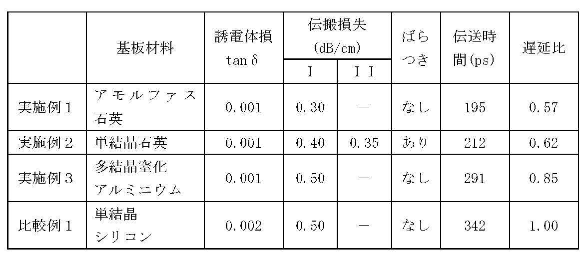
表1から明らかなように、セラミックス材料を用いる本発明の実施例のフォトニック結晶素子は、半導体材料を用いる比較例1のフォトニック結晶素子に比べて電気信号の遅延量を顕著に小さくすることができる。また、伝搬損失を小さくすることができる。さらに、実施例1および3と実施例2とを比較すると明らかなように、多結晶またはアモルファス材料を基板に用いることにより、単結晶を用いる場合のような異方性に起因する特性ばらつき(ここでは、伝搬損失)を防止することができる。
本発明の実施形態によるフォトニック結晶素子は、光導波路、次世代高速通信、センサー、レーザー加工、太陽光発電等の幅広い分野に用いられ得、特に、ミリ波~テラヘルツ波の導波路として好適に用いられ得る。このようなフォトニック結晶素子は、例えば、アンテナ、バンドパスフィルタ、カプラ、遅延線(位相器)、またはアイソレータに用いられ得る。
10 基板
12 空孔
14 高屈折率部
16 導波路
100 フォトニック結晶素子
12 空孔
14 高屈折率部
16 導波路
100 フォトニック結晶素子
Claims (17)
- セラミックス材料の基板に周期的に空孔が形成されてなる2次元フォトニック結晶スラブを有し、
周波数が30GHz以上20THz以下である電磁波を導波する、
フォトニック結晶素子。 - 前記基板の下部に設けられ、該基板を支持する支持基板と、
該基板と該支持基板とを一体化する接合部と、
該基板の下面と該支持基板の上面と該接合部とにより規定される空洞と、
をさらに有する、請求項1に記載のフォトニック結晶素子。 - 前記セラミックス材料が多結晶またはアモルファスである、請求項1または2に記載のフォトニック結晶素子。
- 前記基板における気孔サイズが1μm以上の気孔率が0.5ppm~3000ppmである、請求項1から3のいずれかに記載のフォトニック結晶素子。
- 前記空孔の周期が10μm~1mmである、請求項1から4のいずれかに記載のフォトニック結晶素子。
- 前記基板の100GHz~10THzにおける誘電率が3.6~11.5である、請求項1から5のいずれかに記載のフォトニック結晶素子。
- 前記基板の誘電損失が0.01以下である、請求項1から6のいずれかに記載のフォトニック結晶素子。
- 前記基板の抵抗率が100kΩ・cm以上である、請求項1から7のいずれかに記載のフォトニック結晶素子。
- 前記セラミックス材料が、石英、窒化アルミニウム、酸化アルミニウム、炭化ケイ素、酸化マグネシウム、およびスピネルからなる群から選択される1つである、請求項1から8のいずれかに記載のフォトニック結晶素子。
- 前記基板において前記空孔が形成されていない部分に導波路が規定され、該導波路が、周波数が30GHz以上20THz以下である電磁波を導波する、請求項1から9のいずれかに記載のフォトニック結晶素子。
- アンテナ、バンドパスフィルタ、カプラ、遅延線またはアイソレータとして用いることができる、請求項1から10のいずれかに記載のフォトニック結晶素子。
- 前記基板の下部に設けられ、該基板を支持する支持基板と、
前記電磁波の送信、受信および増幅の少なくともいずれか1つが可能な能動素子であって、前記支持基板に支持されている能動素子と、を備えている、請求項1に記載のフォトニック結晶素子。 - 前記基板において前記空孔が形成されていない部分に規定される線欠陥の第1導波路と、
電磁波の伝搬経路において前記能動素子と前記第1導波路との間に位置し、電磁波を導波可能な第2導波路と、を備えている、請求項12に記載のフォトニック結晶素子。 - 前記基板において前記空孔が形成されていない部分に規定される線欠陥の導波路と、
前記基板において前記空孔が形成されていない部分に規定される共振器であって、電磁波の伝搬経路において前記能動素子と前記導波路との間に位置し、電磁波を導波可能な共振器と、を備えている、請求項12に記載のフォトニック結晶素子。 - 前記基板と前記支持基板とは、直接接合されている、請求項12から14のいずれかに記載のフォトニック結晶素子。
- 前記支持基板は、凹部を有し、
前記フォトニック結晶素子は、前記基板の下面と前記支持基板の凹部とにより規定される空洞を備えている、請求項15に記載のフォトニック結晶素子。 - 前記基板と前記支持基板との間に位置する絶縁層と、
前記基板の下面と前記支持基板の上面と前記絶縁層とにより規定される空洞と、を備えている、請求項15に記載のフォトニック結晶素子。
Priority Applications (5)
| Application Number | Priority Date | Filing Date | Title |
|---|---|---|---|
| JP2021567018A JP7285340B2 (ja) | 2020-07-27 | 2021-07-26 | フォトニック結晶素子 |
| DE112021003953.9T DE112021003953T5 (de) | 2020-07-27 | 2021-07-26 | Photonisches Kristallelement |
| JP2021192761A JP7108119B2 (ja) | 2020-07-27 | 2021-11-29 | フォトニック結晶素子 |
| JP2021192760A JP7108118B2 (ja) | 2020-07-27 | 2021-11-29 | フォトニック結晶素子 |
| US18/062,733 US12645104B2 (en) | 2020-07-27 | 2022-12-07 | Photonic crystal element |
Applications Claiming Priority (2)
| Application Number | Priority Date | Filing Date | Title |
|---|---|---|---|
| JP2020-126208 | 2020-07-27 | ||
| JP2020126208 | 2020-07-27 |
Related Child Applications (1)
| Application Number | Title | Priority Date | Filing Date |
|---|---|---|---|
| US18/062,733 Continuation US12645104B2 (en) | 2020-07-27 | 2022-12-07 | Photonic crystal element |
Publications (1)
| Publication Number | Publication Date |
|---|---|
| WO2022025009A1 true WO2022025009A1 (ja) | 2022-02-03 |
Family
ID=80036200
Family Applications (1)
| Application Number | Title | Priority Date | Filing Date |
|---|---|---|---|
| PCT/JP2021/027594 Ceased WO2022025009A1 (ja) | 2020-07-27 | 2021-07-26 | フォトニック結晶素子 |
Country Status (4)
| Country | Link |
|---|---|
| US (1) | US12645104B2 (ja) |
| JP (3) | JP7285340B2 (ja) |
| DE (1) | DE112021003953T5 (ja) |
| WO (1) | WO2022025009A1 (ja) |
Cited By (2)
| Publication number | Priority date | Publication date | Assignee | Title |
|---|---|---|---|---|
| JP2023180718A (ja) * | 2022-06-10 | 2023-12-21 | 沖電気工業株式会社 | 光導波路素子 |
| DE102024107297A1 (de) * | 2024-03-14 | 2025-09-18 | Universität Duisburg-Essen, Körperschaft des öffentlichen Rechts | Drahtlose Detektion von Pathogen in Luft mit photonischem Kristall |
Families Citing this family (2)
| Publication number | Priority date | Publication date | Assignee | Title |
|---|---|---|---|---|
| JP2542202B2 (ja) | 1986-11-24 | 1996-10-09 | 株式会社 メレツク | ステッピングモ―タの微小角駆動方法とその装置 |
| JP3266557B2 (ja) | 1997-10-07 | 2002-03-18 | マイコム株式会社 | ステッピングモータの微小角駆動装置 |
Citations (6)
| Publication number | Priority date | Publication date | Assignee | Title |
|---|---|---|---|---|
| JP2003227953A (ja) * | 2002-02-06 | 2003-08-15 | Matsushita Electric Ind Co Ltd | フォトニック結晶集光素子、フォトニック結晶集光光源、および光ディスク装置 |
| JP2005274840A (ja) * | 2004-03-24 | 2005-10-06 | Ricoh Co Ltd | 光遅延素子 |
| WO2010073708A1 (ja) * | 2008-12-26 | 2010-07-01 | 日本電気株式会社 | 波長フィルタ |
| JP2015162787A (ja) * | 2014-02-27 | 2015-09-07 | 国立大学法人大阪大学 | 方向性結合器および合分波器デバイス |
| JP2015187716A (ja) * | 2014-03-12 | 2015-10-29 | 国立大学法人大阪大学 | テラヘルツ波デバイス、およびテラヘルツ波集積回路 |
| JP2019082518A (ja) * | 2017-10-30 | 2019-05-30 | 有限会社オートクローニング・テクノロジー | 光マトリクススイッチ |
Family Cites Families (13)
| Publication number | Priority date | Publication date | Assignee | Title |
|---|---|---|---|---|
| JP4658405B2 (ja) * | 2001-08-23 | 2011-03-23 | 三菱電機株式会社 | 高周波用導波路とその製造方法 |
| US7194174B2 (en) * | 2001-10-19 | 2007-03-20 | Ignis Technologies As | Integrated photonic crystal structure and method of producing same |
| GB0302654D0 (en) * | 2003-02-05 | 2003-03-12 | Univ Cambridge Tech | Processes of forming small diameter rods and tubes |
| US6873777B2 (en) | 2003-03-10 | 2005-03-29 | Japan Aviation Electronics Industry Limited | Two-dimensional photonic crystal device |
| CN100337132C (zh) * | 2003-03-26 | 2007-09-12 | Tdk株式会社 | 二维光子晶体及使用此晶体的波导和谐振器 |
| US7440658B2 (en) | 2004-03-03 | 2008-10-21 | Japan Science And Technology Agency | Photonic crystal coupling defect waveguide |
| US7228042B2 (en) * | 2005-03-04 | 2007-06-05 | International Business Machines Corporation | Method and apparatus for resonant coupling in photonic crystal circuits |
| JP2008035017A (ja) * | 2006-07-27 | 2008-02-14 | Murata Mfg Co Ltd | 2次元周期構造を有する高周波デバイス |
| JP4785194B2 (ja) * | 2006-08-25 | 2011-10-05 | 日本碍子株式会社 | スラブ型2次元フォトニック結晶構造の製造方法 |
| JP2008299031A (ja) * | 2007-05-31 | 2008-12-11 | Canon Inc | フォトニック結晶構造およびその製造方法 |
| JP5290737B2 (ja) * | 2008-02-08 | 2013-09-18 | 古河電気工業株式会社 | 光−マイクロ波発振器及びパルス発生装置 |
| JP6281868B2 (ja) | 2013-03-08 | 2018-02-21 | 国立大学法人大阪大学 | フォトニック結晶スラブ電磁波吸収体および高周波金属配線回路、電子部品、および送信器、受信器および近接無線通信システム |
| US11209473B2 (en) * | 2020-03-16 | 2021-12-28 | Quantum Valley Ideas Laboratories | Sensing radio frequency electromagnetic radiation |
-
2021
- 2021-07-26 JP JP2021567018A patent/JP7285340B2/ja active Active
- 2021-07-26 DE DE112021003953.9T patent/DE112021003953T5/de active Pending
- 2021-07-26 WO PCT/JP2021/027594 patent/WO2022025009A1/ja not_active Ceased
- 2021-11-29 JP JP2021192761A patent/JP7108119B2/ja active Active
- 2021-11-29 JP JP2021192760A patent/JP7108118B2/ja active Active
-
2022
- 2022-12-07 US US18/062,733 patent/US12645104B2/en active Active
Patent Citations (6)
| Publication number | Priority date | Publication date | Assignee | Title |
|---|---|---|---|---|
| JP2003227953A (ja) * | 2002-02-06 | 2003-08-15 | Matsushita Electric Ind Co Ltd | フォトニック結晶集光素子、フォトニック結晶集光光源、および光ディスク装置 |
| JP2005274840A (ja) * | 2004-03-24 | 2005-10-06 | Ricoh Co Ltd | 光遅延素子 |
| WO2010073708A1 (ja) * | 2008-12-26 | 2010-07-01 | 日本電気株式会社 | 波長フィルタ |
| JP2015162787A (ja) * | 2014-02-27 | 2015-09-07 | 国立大学法人大阪大学 | 方向性結合器および合分波器デバイス |
| JP2015187716A (ja) * | 2014-03-12 | 2015-10-29 | 国立大学法人大阪大学 | テラヘルツ波デバイス、およびテラヘルツ波集積回路 |
| JP2019082518A (ja) * | 2017-10-30 | 2019-05-30 | 有限会社オートクローニング・テクノロジー | 光マトリクススイッチ |
Cited By (2)
| Publication number | Priority date | Publication date | Assignee | Title |
|---|---|---|---|---|
| JP2023180718A (ja) * | 2022-06-10 | 2023-12-21 | 沖電気工業株式会社 | 光導波路素子 |
| DE102024107297A1 (de) * | 2024-03-14 | 2025-09-18 | Universität Duisburg-Essen, Körperschaft des öffentlichen Rechts | Drahtlose Detektion von Pathogen in Luft mit photonischem Kristall |
Also Published As
| Publication number | Publication date |
|---|---|
| JP2022040119A (ja) | 2022-03-10 |
| JP7108118B2 (ja) | 2022-07-27 |
| JP2022036087A (ja) | 2022-03-04 |
| JPWO2022025009A1 (ja) | 2022-02-03 |
| US12645104B2 (en) | 2026-06-02 |
| US20230112992A1 (en) | 2023-04-13 |
| JP7108119B2 (ja) | 2022-07-27 |
| JP7285340B2 (ja) | 2023-06-01 |
| DE112021003953T5 (de) | 2023-06-07 |
Similar Documents
| Publication | Publication Date | Title |
|---|---|---|
| JP7108118B2 (ja) | フォトニック結晶素子 | |
| JP7319472B2 (ja) | 導波素子 | |
| Liu et al. | Enhancement of the gain for microstrip antennas using negative permeability metamaterial on low temperature co-fired ceramic (LTCC) substrate | |
| McKinzie et al. | 60-GHz $2\times 2$ LTCC patch antenna array with an integrated EBG structure for gain enhancement | |
| Zheng et al. | A compact waveguide slot filtering antenna based on mushroom-type surface | |
| Oskouei et al. | Guided and leaky wave characteristics of periodic defected ground structures | |
| Chang et al. | Planar air-filled terahertz antenna array based on channelized coplanar waveguide using hierarchical silicon bulk micromachining | |
| US20240186672A1 (en) | Waveguide device | |
| JP7602995B2 (ja) | 導波素子および導波素子の製造方法 | |
| Lee et al. | Directive millimetre-wave antenna based on freeformed woodpile EBG structure | |
| Torrisi et al. | Design and characterization of a silicon w-band woodpile photonic crystal waveguide | |
| McKinzie et al. | 60 GHz patch antenna in LTCC with an integrated EBG structure for antenna pattern improvements | |
| Burns et al. | Improvement of planar antenna efficiency when integrated with a millimetre-wave photonic crystal | |
| US20240125986A1 (en) | Member for terahertz equipment | |
| CN117060090B (zh) | 一种宽带圆极化平面集成馈源透射阵天线 | |
| JP7138257B1 (ja) | 導波素子 | |
| Abdellatif et al. | Low-insertion loss phase shifter for millimeter-wave phased array antennas | |
| WO2023017775A1 (ja) | 導波素子 | |
| Liu | Suppression of the mutual coupling between microstrip antenna arrays using negative permeability metamaterial on LTCC substrate | |
| Ren et al. | 3D-printed open-ended waveguide antenna for 60 GHz applications | |
| Beruete et al. | Connection between extraordinary transmission and negative refraction in a prism of stacked sub-wavelength hole arrays | |
| CN118431752B (zh) | 适用于毫米波相控阵的宽波束天线及其设计方法 | |
| Ouassal | Investigation of electromagnetic band-gap structures using metallic open square rings for microwave applications | |
| JP2023026414A (ja) | 導波素子 | |
| Bunea et al. | 28 GHz CRLH antenna on silicon substrate |
Legal Events
| Date | Code | Title | Description |
|---|---|---|---|
| ENP | Entry into the national phase |
Ref document number: 2021567018 Country of ref document: JP Kind code of ref document: A |
|
| 121 | Ep: the epo has been informed by wipo that ep was designated in this application |
Ref document number: 21850053 Country of ref document: EP Kind code of ref document: A1 |
|
| 122 | Ep: pct application non-entry in european phase |
Ref document number: 21850053 Country of ref document: EP Kind code of ref document: A1 |