WO2022019042A1 - 電子回路 - Google Patents
電子回路 Download PDFInfo
- Publication number
- WO2022019042A1 WO2022019042A1 PCT/JP2021/023753 JP2021023753W WO2022019042A1 WO 2022019042 A1 WO2022019042 A1 WO 2022019042A1 JP 2021023753 W JP2021023753 W JP 2021023753W WO 2022019042 A1 WO2022019042 A1 WO 2022019042A1
- Authority
- WO
- WIPO (PCT)
- Prior art keywords
- resistance
- terminal
- resistor
- electronic circuit
- voltage
- Prior art date
- Legal status (The legal status is an assumption and is not a legal conclusion. Google has not performed a legal analysis and makes no representation as to the accuracy of the status listed.)
- Ceased
Links
Images










Classifications
-
- H—ELECTRICITY
- H03—ELECTRONIC CIRCUITRY
- H03H—IMPEDANCE NETWORKS, e.g. RESONANT CIRCUITS; RESONATORS
- H03H5/00—One-port networks comprising only passive electrical elements as network components
- H03H5/12—One-port networks comprising only passive electrical elements as network components with at least one voltage- or current-dependent element
-
- H—ELECTRICITY
- H10—SEMICONDUCTOR DEVICES; ELECTRIC SOLID-STATE DEVICES NOT OTHERWISE PROVIDED FOR
- H10D—INORGANIC ELECTRIC SEMICONDUCTOR DEVICES
- H10D1/00—Resistors, capacitors or inductors
- H10D1/40—Resistors
- H10D1/47—Resistors having no potential barriers
-
- H—ELECTRICITY
- H10—SEMICONDUCTOR DEVICES; ELECTRIC SOLID-STATE DEVICES NOT OTHERWISE PROVIDED FOR
- H10D—INORGANIC ELECTRIC SEMICONDUCTOR DEVICES
- H10D84/00—Integrated devices formed in or on semiconductor substrates that comprise only semiconducting layers, e.g. on Si wafers or on GaAs-on-Si wafers
- H10D84/201—Integrated devices formed in or on semiconductor substrates that comprise only semiconducting layers, e.g. on Si wafers or on GaAs-on-Si wafers characterised by the integration of only components covered by H10D1/00 or H10D8/00, e.g. RLC circuits
- H10D84/204—Integrated devices formed in or on semiconductor substrates that comprise only semiconducting layers, e.g. on Si wafers or on GaAs-on-Si wafers characterised by the integration of only components covered by H10D1/00 or H10D8/00, e.g. RLC circuits of combinations of diodes or capacitors or resistors
- H10D84/209—Integrated devices formed in or on semiconductor substrates that comprise only semiconducting layers, e.g. on Si wafers or on GaAs-on-Si wafers characterised by the integration of only components covered by H10D1/00 or H10D8/00, e.g. RLC circuits of combinations of diodes or capacitors or resistors of only resistors
-
- H—ELECTRICITY
- H10—SEMICONDUCTOR DEVICES; ELECTRIC SOLID-STATE DEVICES NOT OTHERWISE PROVIDED FOR
- H10D—INORGANIC ELECTRIC SEMICONDUCTOR DEVICES
- H10D84/00—Integrated devices formed in or on semiconductor substrates that comprise only semiconducting layers, e.g. on Si wafers or on GaAs-on-Si wafers
- H10D84/01—Manufacture or treatment
- H10D84/02—Manufacture or treatment characterised by using material-based technologies
- H10D84/03—Manufacture or treatment characterised by using material-based technologies using Group IV technology, e.g. silicon technology or silicon-carbide [SiC] technology
- H10D84/038—Manufacture or treatment characterised by using material-based technologies using Group IV technology, e.g. silicon technology or silicon-carbide [SiC] technology using silicon technology, e.g. SiGe
Definitions
- This disclosure relates to electronic circuits.
- the resistance value of the 3-terminal configuration changes depending on the voltage applied to the sub-terminals.
- This change in resistance can be one of the causes of distortion in electronic circuits.
- a configuration is conceivable in which the voltage dependence of the resistance can be canceled by the resistance ratio by applying an input-dependent correction voltage to the sub-terminal of the resistance on the input side.
- this method is effective only in a configuration using an operational amplifier, and an additional circuit for correction is required, so that an increase in power consumption is unavoidable. Further, the correction circuit to be added also needs to guarantee the accuracy for correcting the resistance distortion.
- an electronic circuit that suppresses distortion of a 3-terminal resistor is provided.
- the electronic circuit includes a first resistor and a second resistor.
- the first resistance has a structure of resistance to voltage between the first terminal and the second terminal, and the first terminal is directly or indirectly connected to the input.
- the second resistance has a structure of resistance to voltage between the first terminal and the second terminal, and the first terminal is directly or indirectly connected to the second terminal of the first resistance. 2 terminals are connected to the output.
- the second terminal of the second resistance is directly or indirectly connected to the third terminal that changes the resistance value of the first resistance by a voltage.
- the first terminal of the first resistance may be connected to the third terminal that changes the resistance value of the second resistance by a voltage.
- the same configuration may be obtained even when the first terminal of the first resistance is connected to the output and the second terminal of the second resistance is connected to the input.
- a third resistance having a first terminal, a second terminal, and a third terminal, and a fourth resistance having the first terminal, the second terminal, and the third terminal may be further provided, and the first resistance and the first resistance may be further provided.
- the first resistance group formed by the two resistances, the second terminal of the third resistance and the first terminal of the fourth resistance formed by the third resistance and the fourth resistance are at least direct.
- the first resistance group and the second resistance group are connected in series.
- the third terminal is the first terminal or the second terminal of the other resistance of the resistance group to which the third terminal belongs. It may be connected to a terminal.
- a third resistor having a first terminal, a second terminal, and a third terminal, and the second terminal being connected to the first terminal of the first resistor, and a first terminal, a second terminal, and a third terminal.
- a fourth resistor may be further provided, wherein the first terminal is connected to the second terminal of the second resistor.
- the third resistance, the first resistance, the second resistance, and the fourth resistance may have symmetry in this order.
- the first resistance group having the third resistance In the first resistance group having the third resistance, the first resistance, the second resistance, the fourth resistance, and the second resistance group which is another resistance group having symmetry, the first resistance group
- the second resistance group is connected in series or in parallel, and in any of the resistances belonging to the first resistance group and the second resistance group, the third terminal is other than the resistance group to which it belongs. It may be connected to the first terminal or the second terminal of the resistor of.
- a circuit diagram of an electronic circuit according to an embodiment A circuit diagram of an electronic circuit according to an embodiment. A circuit diagram of an electronic circuit according to an embodiment. A circuit diagram of an electronic circuit according to an embodiment. A circuit diagram of an electronic circuit according to an embodiment. A circuit diagram of an electronic circuit according to an embodiment. A circuit diagram of an electronic circuit according to an embodiment. A circuit diagram of an electronic circuit according to an embodiment. A circuit diagram of an electronic circuit according to an embodiment. A circuit diagram of an electronic circuit according to an embodiment. A circuit diagram of an electronic circuit according to an embodiment. A circuit diagram of an electronic circuit according to an embodiment. A circuit diagram of an electronic circuit according to an embodiment. A circuit diagram of an electronic circuit according to an embodiment. A circuit diagram of an electronic circuit according to an embodiment. A circuit diagram of an electronic circuit according to an embodiment. A circuit diagram of an electronic circuit according to an embodiment. A circuit diagram of an electronic circuit according to an embodiment. A circuit diagram of an electronic circuit according to an embodiment. A circuit diagram of an electronic circuit according to an embodiment. A circuit diagram of an electronic circuit according to an embodiment. A circuit diagram
- a circuit diagram of an electronic circuit according to an embodiment A circuit diagram of an electronic circuit according to an embodiment. A circuit diagram of an electronic circuit according to an embodiment. A circuit diagram of an electronic circuit according to an embodiment. A circuit diagram of an electronic circuit according to an embodiment. A circuit diagram of an electronic circuit according to an embodiment. A circuit diagram of an electronic circuit according to an embodiment. A circuit diagram of an electronic circuit according to an embodiment. A circuit diagram of an electronic circuit according to an embodiment. A circuit diagram of an electronic circuit according to an embodiment. A circuit diagram of an electronic circuit according to an embodiment. A circuit diagram of an electronic circuit according to an embodiment. A circuit diagram of an electronic circuit according to an embodiment. A circuit diagram of an electronic circuit according to an embodiment. A circuit diagram of an electronic circuit according to an embodiment. A circuit diagram of an electronic circuit according to an embodiment. A circuit diagram of an electronic circuit according to an embodiment. A circuit diagram of an electronic circuit according to an embodiment. A circuit diagram of an electronic circuit according to an embodiment. A circuit diagram of an electronic circuit according to an embodiment. A circuit diagram of an electronic circuit according to an embodiment. A circuit diagram
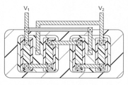
- the layout diagram of the electronic circuit which concerns on one Embodiment. A cross-sectional view of the layout of an electronic circuit according to an embodiment.
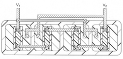
- the layout diagram of the electronic circuit which concerns on one Embodiment. The layout diagram of the electronic circuit which concerns on one Embodiment.
- FIG. 1 shows a circuit diagram of an electronic circuit according to an embodiment.
- the first resistance network 10 includes a first resistance R1 and a second resistance R2, which are two three-terminal resistors.
- the resistance value of the 3-terminal resistor changes depending on the voltage applied to the sub-terminals.
- the terminals connected as resistors will be referred to as the 1st terminal and the 2nd terminal, and the above sub-terminals will be referred to as the 3rd terminal.
- the resistance value of the first resistor R1 is described as R1, but depending on the context, it should be read whether it represents a circuit element or a resistance value.
- the first terminal in the first resistance R1, the first terminal is connected to the outside and the second terminal is connected in series with the second resistance R2.
- the first terminal is connected to the second terminal of the first resistance R1
- the second terminal is connected to the outside
- the second terminal is connected to the third terminal of the first resistance R1.
- the first resistance network 10 in the present embodiment is a circuit related to a resistance network having a plurality of resistances.
- the first resistance network 10 is provided with, for example, an input terminal and an output terminal, and these terminals are arranged in a circuit so as to be connected between the voltages V1 and V2. Then, the first resistance network 10 functions as a resistance network between the voltage V1 and the voltage V2.
- FIG. 2 shows a circuit diagram according to another example of the first resistance network 10 implemented based on the configuration of FIG.
- the connection of the first resistance R1 is the same as the example shown in FIG.
- the third terminal of the second resistor R2 is further connected to the first terminal of the first resistor R1.
- the first resistance network 10 has symmetry in which the structure does not change with respect to the replacement of the terminals of the entire circuit. Having symmetry means having the same function even if the terminals connected to the voltages V1 and V2 are exchanged, for example. In order to ensure this symmetry, it is preferable that the resistance value of the first resistor R1 and the resistance value of the second resistor R2 have the same characteristics. That is, it is desirable that the same resistance element is used for the first resistance R1 and the second resistance R2.
- the 3rd terminal of the 2nd resistance R2 is connected to the 1st terminal which is the farthest terminal of the 1st resistance R1 when viewed from the 2nd resistance R2.
- the terminals of the first resistance R1 and the second resistance R2 may be connected to each other in a so-called “sliding state”.
- R0 is a resistance value in a state where the voltage of the third terminal is the midpoint of the voltage of the first terminal and the second terminal
- k is the effective area of the material (for example, polysilicon) forming the resistance. It is a coefficient determined from and the depletion layer, and typically satisfies k ⁇ 1.
- the term over which k is applied in this equation (1) is the first-order distortion of the resistance.
- the resistance value is expressed as follows.
- the voltage between the first resistance R1 and the second resistance R2 that is, the potential at the second terminal of the first resistance R1 and the first terminal of the second resistance R2 is defined as Vc.
- Vc is expressed by dividing V1 and V2 by the ratio of the resistance values of the first resistance R1 and the second resistance R2, using equation (1) for R1 and R2, the following equation is used. (4) holds.
- equation (6) is an upwardly convex function with respect to voltage. From this, it is possible to reduce the influence of the second-order distortion of the resistance on the voltage by connecting a resistor (network) having a second-order distortion characteristic that is convex downward with respect to the voltage.
- the first resistance network 10 As described above, according to the first resistance network 10 according to the present embodiment, it is possible to form a resistance having characteristics with respect to an upwardly convex secondary voltage.
- FIG. 3 is a diagram showing an example of a second resistance network that suppresses secondary distortion due to the voltage of the first resistance network 10 shown in FIG.
- the second resistance network 10 includes a third resistance R3 and a fourth resistance R4.
- the 3rd resistor R3 is connected to the 1st terminal and the 3rd terminal, and is connected in series with the 4th resistor R4.
- the 4th resistance R4 is connected to the 2nd terminal and the 3rd terminal, and the 1st terminal is connected to the 2nd terminal of the 3rd resistance R3.
- This combined resistance value R is expressed as follows.
- Vc is expressed as follows.
- the combined resistance value R can be obtained as follows by performing the same equation conversion as above.
- the resistance value of the second resistance network 20 in FIG. 3 has a second-order distortion of the downwardly convex voltage.
- FIG. 4 is a diagram showing an example of a second resistance network that suppresses secondary distortion due to the voltage of the first resistance network 10 shown in FIG. 2 having a configuration different from that of FIG.
- the second resistance network 10 includes a third resistance R3 and a fourth resistance R4.
- the 3rd resistor R3 is connected to the 2nd terminal and the 3rd terminal, and is connected in series with the 4th resistor R4.
- the 4th resistor R4 is connected to the 1st terminal and the 3rd terminal, and the 1st terminal is connected to the 2nd terminal of the 3rd resistor R3.
- This combined resistance value R is expressed as follows.
- Vc is expressed as follows.
- the combined resistance value R can be obtained as follows by performing the same equation conversion as above.
- the resistance value of the second resistance network 20 in FIG. 4 has a second-order distortion of the downwardly convex voltage. That is, it has the same characteristics as in the case of FIG.
- FIG. 5 is a diagram showing an electronic circuit in which a resistance network according to an embodiment is combined.
- the electronic circuit 1 connects the first resistance network 10 shown in FIG. 2 and the second resistance network 20 shown in FIG. 3 in series.
- FIG. 6 is a diagram showing an electronic circuit in which a resistance network according to an embodiment is combined.
- the electronic circuit 1 connects the first resistance network 10 shown in FIG. 2 and the second resistance network 20 shown in FIG. 4 in series.
- each resistance network is connected in series, but the resistance network is not limited to the series and may be connected in parallel. That is, by combining the first resistance network 10 and the second resistance network 20 in parallel, it is possible to suppress the second-order distortion of the resistance value caused by the voltage.
- each of the electronic circuits 1 listed below (1) It has symmetry in the connection of resistors. (2) At least one resistor (at least two from symmetry), a voltage is applied from the terminal farther from the other resistance to the third terminal. Have in common. This property is shown, for example, as a combination of resistances represented by Eqs. (2), (6), (9), and (12).
- the electronic circuit preferably includes both a first resistance network 10 and a second resistance network 20.
- the resistance in the first network 10 has the same characteristics, and the resistance in the second network 20 has the same characteristics.
- the resistance in the first network 10 and the resistance in the second network 20 do not have to have the same characteristics, for example, a combination having characteristics such that the upper and lower convexities of the second-order distortion of the voltage are canceled out. May be.
- FIG. 7 shows an example of connecting a resistor having the symmetry described above.
- the resistors shown in FIG. 7 are the first resistance R1 and the second resistance R2, and the third terminal of the third resistance R3 is the second terminal far from the third resistance R3 of the first resistance R1. It is connected, and the third terminal of the fourth resistor R4 is connected to the first terminal, which is a terminal far from the fourth resistor R4 of the second resistor R2.
- the electronic circuit 1 Focusing on the first resistance R1 and the second resistance R2, the electronic circuit 1 includes the first resistance network 10 shown in FIG. 2, and focusing on the third resistance R3 and the fourth resistance R4, the second resistance shown in FIG. Equipped with network 20.
- FIG. 8 shows an example of connecting a resistor having the symmetry described above.
- the first resistance R1 and the second resistance R2 are crossed, the third terminal of the third resistance R3 is connected to the second terminal on the far side of the first resistance R1, and the fourth resistance R4.
- the third terminal of is connected to the first terminal on the far side of the second resistor R2.
- the electronic circuit 1 Focusing on the first resistance R1 and the second resistance R2, the electronic circuit 1 includes the first resistance network 10 shown in FIG. 2, and focusing on the third resistance R3 and the fourth resistance R4, the second resistance shown in FIG. Equipped with network 20.
- FIG. 9 shows an example of connecting a resistor having the symmetry described above.
- the third terminal of the first resistance R1 is connected to the first terminal
- the third terminal of the second resistance R2 is connected to the second terminal
- the third terminal of the third resistance R3 is the third terminal. 1 It is connected to the 2nd terminal on the far side of the resistor R1
- the 3rd terminal of the 4th resistor R4 is connected to the 1st terminal on the far side of the 2nd resistor R2.
- FIG. 10 shows an example of connecting a resistor having the symmetry described above.
- the third terminal of the first resistance R1 is connected to the second terminal
- the third terminal of the second resistance R2 is connected to the first terminal
- the third terminal of the third resistance R3 is the third terminal. 1 It is connected to the 2nd terminal on the far side of the resistor R1
- the 3rd terminal of the 4th resistor R4 is connected to the 1st terminal on the far side of the 2nd resistor R2.
- FIG. 11 shows an example of connecting a resistor having the symmetry described above.
- the first resistance R1 and the second resistance R2 are in contact with each other, the third terminal of the third resistance R3 is connected to the first terminal, and the third terminal of the fourth resistance R4 is the second terminal. Connected to the terminal.
- the electronic circuit 1 Focusing on the first resistance R1 and the second resistance R2, the electronic circuit 1 includes the first resistance network 10 shown in FIG. 2, and focusing on the third resistance R3 and the fourth resistance R4, the second resistance shown in FIG. Equipped with network 20.
- FIG. 12 shows an example of connecting a resistor having the symmetry described above.
- the first resistance R1 and the second resistance R2 are connected to each other via the third resistance R3 and the fourth resistance R4, respectively, and the third terminal of the third resistance R3 is connected to the first terminal. Then, the third terminal of the fourth resistor R4 is connected to the second resistor.
- the electronic circuit 1 Focusing on the first resistance R1 and the second resistance R2, the electronic circuit 1 includes the first resistance network 10 shown in FIG. 2, and focusing on the third resistance R3 and the fourth resistance R4, the second resistance shown in FIG. Equipped with network 20.
- FIG. 13 shows an example of connecting a resistor having the symmetry described above.
- the third terminal of the first resistance R1 is connected to the first terminal on the far side of the third resistance R3, and the third terminal of the second resistance R2 is the far side of the fourth resistance R4. It is connected to the 2nd terminal, the 3rd terminal of the 3rd resistance R3 is connected to the 2nd terminal, and the 3rd terminal of the 4th resistance R4 is connected to the 1st terminal.
- FIG. 14 shows an example of connecting a resistor having the symmetry described above.
- the first resistance R1 and the second resistance R2 are in contact with each other, the third terminal of the third resistance R3 is connected to the second terminal, and the third terminal of the fourth resistance R4 is the first terminal. Connected to the terminal.
- the electronic circuit 1 Focusing on the first resistance R1 and the second resistance R2, the electronic circuit 1 includes the first resistance network 10 shown in FIG. 2, and focusing on the third resistance R3 and the fourth resistance R4, the first resistance R1 and the second resistance R1 and the second resistance R4.
- the second resistor network 20 shown in FIG. 4 is provided via the resistor R2.
- FIG. 15 shows an example of connecting a resistor having the symmetry described above.
- the first resistance R1 and the second resistance R2 are connected via the third resistance R3 and the fourth resistance R4, respectively, and the third terminal of the third resistance R3 is connected to the second terminal. Then, the third terminal of the fourth resistor R4 is connected to the first terminal.
- the electronic circuit 1 Focusing on the first resistance R1 and the second resistance R2, the electronic circuit 1 includes the first resistance network 10 shown in FIG. 2, and focusing on the third resistance R3 and the fourth resistance R4, the second resistance shown in FIG. Equipped with network 20.
- FIG. 16 shows an example of connecting a resistor having the symmetry described above.
- the resistance shown in FIG. 16 is a combination of the third resistance R3, the first resistance R1 and the fourth resistance R4, and the fourth resistance R4, the second resistance R2 and the third resistance R3. ..
- the electronic circuit 1 Focusing on the first resistance R1 and the second resistance R2, the electronic circuit 1 includes the second resistance network 20 shown in FIG. 3, and focusing on the third resistance R3 and the fourth resistance R4, the first resistance shown in FIG. Equipped with network 10.
- FIG. 17 shows an example of connecting a resistor having the symmetry described above.
- the third terminal and the first terminal of the first resistance R1 are connected, the third terminal and the second terminal of the second resistance R2 are connected, and the third resistance R3 and the fourth resistance R4 are connected. It is a sash.
- the electronic circuit 1 Focusing on the first resistance R1 and the second resistance R2, the electronic circuit 1 includes the second resistance network 20 shown in FIG. 3, and focusing on the third resistance R3 and the fourth resistance R4, the first resistance shown in FIG. Equipped with network 10.
- FIG. 18 shows an example of connecting a resistor having the symmetry described above.
- the third terminal and the second terminal of the first resistance R1 are connected, the third terminal and the first terminal of the second resistance R2 are connected, and the third resistance R3 and the fourth resistance R4 are connected. It is a sash.
- the electronic circuit 1 Focusing on the first resistance R1 and the second resistance R2, the electronic circuit 1 includes the second resistance network 20 shown in FIG. 4, and focusing on the third resistance R3 and the fourth resistance R4, the first resistance shown in FIG. Equipped with network 10.
- FIG. 19 shows an example of connecting a resistor having the symmetry described above.
- the resistors shown in FIG. 19 are the first resistance R1 and the second resistance R2, the first resistance R1 and the fourth resistance R4, the second resistance R2 and the third resistance R3, and the third resistance R3 and the fourth resistance R4, respectively. It is a sash.
- FIG. 20 shows an example of connecting a resistor having the symmetry described above.
- the resistances shown in FIG. 20 are linked by the first resistance R1 and the second resistance R2, and the third resistance R3 and the fourth resistance R4, respectively.
- FIG. 21 shows an example of connecting a resistor having the symmetry described above.
- the third terminal of the first resistance R1 is connected to the first terminal on the far side of the third resistance R3, and the third terminal of the second resistance R2 is the far side of the fourth resistance R4.
- the 3rd terminal of the 3rd resistance R3 is connected to the 2nd terminal on the far side of the 2nd resistance R2
- the 3rd terminal of the 4th resistance R4 is the 1st terminal on the far side of the 1st resistance R1. Is connected to.
- FIG. 22 shows an example of connecting a resistor having the symmetry described above.
- the third terminal of the first resistance R1 is connected to the first terminal
- the third terminal of the second resistance R2 is connected to the second terminal
- the third terminal of the third resistance R3 is the third terminal. It is connected to the 2nd terminal on the far side of the 2 resistance R2, and the 3rd terminal of the 4th resistance R4 is connected to the 1st terminal on the far side of the 1st resistance R1.
- FIG. 23 shows an example of connecting a resistor having the symmetry described above.
- the third terminal of the first resistance R1 is connected to the second terminal
- the third terminal of the second resistance R2 is connected to the first terminal
- the third terminal of the third resistance R3 is the third terminal. It is connected to the 2nd terminal on the far side of the 2 resistance R2, and the 3rd terminal of the 4th resistance R4 is connected to the 1st terminal on the far side of the 1st resistance R1.
- FIG. 24 shows an example of connecting a resistor having the symmetry described above.
- the first resistance R1 and the second resistance R2 are crossed, and the third terminal of the third resistance R3 is connected to the second terminal on the far side of the second resistance R2, and the fourth resistance R4 The third terminal of is connected to the first terminal on the far side of the first resistor R1.
- FIG. 25 shows an example of connecting a resistor having the symmetry described above.
- the first resistance R1 and the second resistance R2 are connected via the third resistance R3 and the fourth resistance R4, and the third terminal of the third resistance R3 is on the far side of the second resistance R2.
- the third terminal of the fourth resistor R4 is connected to the first terminal on the far side of the first resistor R1.
- the resistance value of the electronic circuit 1 as a whole has a large amount of change depending on the voltage, and has a downwardly convex characteristic.
- 17 and 18 show that the resistance value of the electronic circuit 1 as a whole has a large amount of change depending on the voltage and has an upwardly convex characteristic.
- the resistance value of the electronic circuit 1 as a whole has a small amount of change depending on the voltage and has a downwardly convex characteristic.
- the resistance value of the electronic circuit 1 as a whole has a small amount of change depending on the voltage and has an upwardly convex characteristic.
- the resistance value of each resistor may be appropriately adjusted so as to cancel the distortion.
- Two or more resistance networks formed with symmetry using the four resistance elements described above may be combined. For example, here are some examples of combining the two.
- FIG. 26 shows a connection example in which resistance groups having the symmetry described above are connected in series. As shown in FIG. 26, the electronic circuit 1 of FIG. 7 and the electronic circuit 1 of FIG. 11 may be combined to form a resistor as a new electronic circuit 1.
- FIG. 27 shows a connection example in which resistance groups having the symmetry described above are connected in series.
- a resistor may be configured as a new electronic circuit 1 by combining the electronic circuit 1 of FIG. 8 and a group of resistors having symmetry in which four resistors are connected in series.
- the circuit shown in FIG. 27 is a series in which the input of the circuit of FIG. 8 and the output of the circuit obtained by modifying the circuit of FIG. 9 are connected in series. More specifically, the third terminal of the first resistor R1 in FIG. 9 is connected to the first terminal of the third resistor R3, and the third terminal of the second resistor R2 is connected to the second terminal of the fourth resistor R4. The circuit is connected in series with the circuit shown in FIG.
- FIG. 28 shows a connection example in which resistance groups having the symmetry described above are connected in series.
- a resistor may be configured as a new electronic circuit 1 by combining the electronic circuit 1 of FIG. 22 and a group of resistors having symmetry in which four resistors are connected in series.
- the circuit shown in FIG. 28 is a series in which the input of the circuit of FIG. 22 and the output of the circuit obtained by modifying the circuit of FIG. 11 are connected in series. More specifically, the third terminal of the first resistor R1 in FIG. 11 is connected to the second terminal, and the third terminal of the second resistor R2 is connected to the first terminal.
- FIG. 29 shows a connection example in which resistance groups having the symmetry described above are connected in series. As shown in FIG. 29, the electronic circuit 1 of FIG. 13 and the electronic circuit 1 of FIG. 21 may be combined to form a resistor as a new electronic circuit 1.
- FIG. 30 shows a connection example in which resistance groups having the symmetry described above are connected in series. As shown in FIG. 30, the electronic circuit 1 of FIG. 10 and the electronic circuit 1 of FIG. 18 may be combined to form a resistor as a new electronic circuit 1.
- FIG. 31 shows a connection example in which resistance groups having the symmetry described above are connected in series.
- a resistor may be configured as a new electronic circuit 1 by combining the electronic circuit 1 of FIG. 12 and a group of resistors having symmetry in which four resistors are connected in series.
- the circuit shown in FIG. 31 is a series in which the input of the circuit of FIG. 12 and the output of the circuit obtained by modifying the circuit of FIG. 9 are connected in series. More specifically, the third terminal of the third resistor R3 in FIG. 9 is connected to the first terminal, and the third terminal of the fourth resistor R4 is connected to the second terminal.
- All of the electronic circuits 1 listed above can suppress the secondary distortion of the voltage value applied to the sub-terminal (third terminal) of the resistor in the three-terminal resistor. According to such an example, the distortion characteristic of the resistance due to the voltage dependence can be reduced without the need for an additional circuit such as a comparator and a voltage generator. Since a correction circuit other than the resistance element is not required, it is possible to suppress an increase in power consumption due to the addition of such a correction circuit. Further, the polarities, materials, and the like of the resistors are not limited to the same as long as they have the same characteristics.
- the electronic circuit 1 may have symmetry as a whole, or the electronic circuit 1 may have symmetry as shown in FIGS. 5, 6, and 26 to 31. It may be configured to be provided with a plurality of electronic circuits to be provided. Further, the number of resistors is not limited to eight in the present disclosure, and electronic circuit 1 having more symmetry may be connected.
- the resistance group (resistance network) is connected in series, but for example, in the examples of FIGS. 26 to 31, distortion is reduced by connecting the resistance networks in parallel instead of in series. You may.
- the third terminal of each resistance is connected to the first terminal or the second terminal of the other resistance to which the resistance belongs. Please note that there is.
- FIG. 32 is a diagram showing, for example, the vibration of the resistance value as a whole (amount that changes depending on the voltage) in some electronic circuits 1 when a voltage that vibrates sine and cosine is input as a signal.
- the solid line shows the resistance value of the electronic circuit 1 shown in FIG. 6, the dotted line shows the resistance value of the electronic circuit 1 shown in FIG. 2, and the broken line shows the resistance value of the electronic circuit 1 shown in FIG. 3 or FIG.
- the resistance value of the electronic circuit 1 shown in FIG. 6 can be changed in a very small amount depending on the voltage as compared with the case where two resistors are provided.
- the amplitude of the dotted line is 468.8 m ⁇ and the amplitude of the broken line is 155.8 m ⁇ , whereas the amplitude of the solid line (change amount).
- Is 667n ⁇ which is an amplitude (change amount) of about 1 / 200,000 to 1 / 700,000. Further, according to each combination described above, it is possible to further reduce the value of the amplitude (change amount).
- a voltage is applied to the sub-terminal of the 3-terminal resistor at least at the terminal on the far side of the other resistor connected in series with the 3-terminal resistor.
- FIG. 2 An example of the layout of the circuit diagram shown in FIG. 2, which is the basic form of the first resistance network 10 provided in the electronic circuit 1 in the present embodiment, will be described.
- FIG. 33 is a plan view showing the layout of the circuit diagram shown in FIG.
- the first resistance R1 and the second resistance R2 are resistances formed on the semiconductor substrate.
- FIG. 34 is a cross-sectional view taken along the line AA of FIG. 33.
- the layout, cross section, etc. below are examples, and the forms in the present disclosure are not limited to these. Further, the following conductive type is described only as an example, and is not limited to the conductive type.
- Both the first resistor R1 and the second resistor R2 may be generated on the semiconductor substrate.
- the semiconductor substrate is a P-type substrate 200.
- N-type wells 202 are formed on the semiconductor substrate, and P-type wells 204 and 206 are formed on the N-type wells. Resistance is formed on this well region.
- the P-shaped wells 204 and 206 may be metal.
- An insulating film 208 is formed on the P-shaped well region 204, and a polysilicon 212 is formed on the insulating film 208, and this polysilicon 212 plays a role of resistance.
- an insulating film 210 is formed on the well 206, and a polysilicon 214 is formed on the insulating film 210, and the polysilicon 214 functions as a resistor.
- the conductor 100 is provided as a terminal to which the voltage of V1 is applied, that is, as the above-mentioned input terminal (or output terminal).
- the conductor 102 is provided as a terminal to which the voltage of V2 is applied, that is, an output terminal (or an input terminal) described above.
- the voltage applied to the conductor 100 is applied to the polysilicon 212 via the via 120 (first terminal).
- the polysilicon 212 is then connected to the conductor 104 via the via 122 (second terminal) in different regions.
- the conductor 104 is connected to the polysilicon 214 via the via 126 (first terminal) at the other end.
- the polysilicon 214 connects to the conductor 102, i.e., the output terminal, via the via 124 (second terminal) in different regions. In this way, the polysilicon 212, 214 form a resistor connected in series.
- the input terminal and output terminal are connected to the third terminal of the resistor. This connection will be described.
- the conductor 100 is connected to a conductor 108 different from the above via the via 100.
- the conductor 108 connects to the electrode 114 (third terminal) on the well 206 via the via 130, the conductor 110 and the contact 132 on the second resistance R2.
- a voltage is applied to the well 206 by this electrode 114, and the resistance value fluctuates.
- the conductor 102 is connected to the electrode 112 (third terminal) on the first resistor R1 via the conductor 106 and the contact 134.
- a voltage is applied to the well 204 by the electrode 112, and the resistance value fluctuates.
- the first resistor R1 and the second resistor R2 may be formed on the same semiconductor substrate as resistors each having a well region. Then, by connecting in this way, the same voltage is applied to the first terminal of the first resistor R1 and the third terminal of the second resistor R2, and the second terminal of the second resistor R2 and the third terminal of the first resistor R1 are connected. The same voltage can be applied to the terminals.
- FIGS. 35 and 36 show another example on this substrate. As shown in FIG. 35, the first resistance R1 may be divided and arranged on the same well. The same applies to the second resistance R2.
- the first resistance R1 may be divided and arranged on different wells. The same applies to the second resistance R2.
- first resistance which has a structure of resistance to voltage between the first terminal and the second terminal, and the first terminal is directly or indirectly connected to the input. It has a structure of resistance to voltage between the first terminal and the second terminal, the first terminal is directly or indirectly connected to the second terminal of the first resistance, and the second terminal is connected to the output.
- the second resistance and Equipped with The second terminal of the second resistance is directly or indirectly connected to the third terminal whose resistance value of the first resistance is changed by a voltage. Electronic circuit.
- the first terminal of the first resistance is connected to the third terminal whose resistance value of the second resistance is changed by a voltage. Electronic circuit.
- the first resistance group formed by the first resistance and the second resistance, Formed by the third resistance and the fourth resistance, the second terminal of the third resistance and the first terminal of the fourth resistance are at least connected to each other to have symmetry, and to the first resistance group.
- the first resistance group and the second resistance group are connected in series or in parallel.
- the third terminal is connected to the first terminal or the second terminal of the other resistances of the resistance group to which the third terminal belongs.
- a third resistor having a first terminal, a second terminal, and a third terminal, wherein the second terminal is connected to the first terminal of the first resistor.
- a fourth resistor having a first terminal, a second terminal, and a third terminal, wherein the first terminal is connected to the second terminal of the second resistor.
- the first resistance group and the second resistance group are connected in series or in parallel.
- the third terminal is connected to the first terminal or the second terminal of the other resistances of the resistance group to which the third terminal belongs.
- the aspect of the present disclosure is not limited to the above-mentioned embodiment, but also includes various possible modifications, and the effect of the present disclosure is not limited to the above-mentioned contents.
- the components in each embodiment may be applied in appropriate combinations. That is, various additions, changes and partial deletions are possible without departing from the conceptual idea and purpose of the present disclosure derived from the contents specified in the claims and their equivalents.
Landscapes
- Semiconductor Integrated Circuits (AREA)
- Filters And Equalizers (AREA)
- Details Of Resistors (AREA)
Abstract
[課題]3端子抵抗の歪みを抑制する。 [解決手段]電子回路は、第1抵抗と、第2抵抗と、を備える。前記第1抵抗は、第1端子と第2端子間で電圧に対する抵抗の構成を有し、前記第1端子が、直接的に又は間接的に入力と接続される。前記第2抵抗は、第1端子と第2端子間で電圧に対する抵抗の構成を有し、前記第1端子が、直接的に又は間接的に前記第1抵抗の第2端子と接続される。前記電子回路は、前記第1抵抗の抵抗値を電圧により変動させる第3端子に、前記第2抵抗の前記第2端子が、直接的に又は間接的に接続される。
Description
本開示は、電子回路に関する。
3端子構成の抵抗は、サブ端子に印加されている電圧に依存して抵抗値が変わる。この抵抗値の変化が電子回路における歪みの1つの原因となり得る。これに対して、入力側の抵抗のサブ端子に、入力依存の補正電圧を印加することにより抵抗比により抵抗の電圧依存性を打ち消すことを可能とする構成が考えられる。しかしながら、この方式は、オペアンプを用いた構成においてのみ有効であり、かつ、補正用の追加回路が必要となるため、消費電力の増加が避けられない。また、追加する補正回路にも、抵抗歪みを補正するための精度の担保が必要となる。
そこで、本開示では、3端子抵抗の歪みを抑制する電子回路を提供する。
一実施形態によれば、電子回路は、第1抵抗と、第2抵抗と、を備える。前記第1抵抗は、第1端子と第2端子間で電圧に対する抵抗の構成を有し、前記第1端子が、直接的に又は間接的に入力と接続される。前記第2抵抗は、第1端子と第2端子間で電圧に対する抵抗の構成を有し、前記第1端子が、直接的に又は間接的に前記第1抵抗の第2端子と接続され、第2端子が出力と接続される。前記電子回路は、前記第1抵抗の抵抗値を電圧により変動させる第3端子に、前記第2抵抗の前記第2端子が、直接的に又は間接的に接続される。
前記第2抵抗の抵抗値を電圧により変動させる第3端子に、前記第1抵抗の前記第1端子が接続されてもよい。
前記第1抵抗の前記第1端子を前記出力に接続し、前記第2抵抗の前記第2端子を前記入力に接続した場合においても同じ構成となる対称性を有してもよい。
第1端子、第2端子、第3端子を有する第3抵抗と、第1端子、第2端子、第3端子を有する第4抵抗と、をさらに備えてもよく、前記第1抵抗と前記第2抵抗により形成される、第1抵抗群と、前記第3抵抗と前記第4抵抗により形成され、前記第3抵抗の前記第2端子と、前記第4抵抗の前記第1端子が少なくとも直接的又は間接的に接続され、対称性を有し、前記第1抵抗群とは異なる接続の構成を有する、第2抵抗群とにおいて、前記第1抵抗群と、前記第2抵抗群が、直列、又は、並列に接続され、前記第1抵抗群及び前記第2抵抗群に属するいずれの抵抗においても、前記第3端子は、自身が属する抵抗群の他の抵抗の前記第1端子又は前記第2端子と接続されてもよい。
第1端子、第2端子、第3端子を有し、前記第2端子が前記第1抵抗の前記第1端子と接続される、第3抵抗と、第1端子、第2端子、第3端子を有し、前記第1端子が前記第2抵抗の前記第2端子と接続される、第4抵抗と、をさらに備えてもよい。
前記第3抵抗、前記第1抵抗、前記第2抵抗、前記第4抵抗の順番で対称性を有していてもよい。
前記第3抵抗、前記第1抵抗、前記第2抵抗、前記第4抵抗を有する第1抵抗群と、対称性を有する他の抵抗群である第2抵抗群と、において、前記第1抵抗群と、前記第2抵抗群が、直列、又は、並列に接続され、前記第1抵抗群及び前記第2抵抗群に属するいずれの抵抗においても、前記第3端子は、自身が属する抵抗群の他の抵抗の前記第1端子又は前記第2端子と接続されてもよい。
以下、図面を参照して本開示における実施形態の説明をする。図面は、説明のために用いるものであり、実際の装置における各部の構成の形状、サイズ、又は、他の構成とのサイズの比等が図に示されている通りである必要はない。また、図面は、簡略化して書かれているため、図に書かれている以外にも実装上必要な構成は、適切に備えるものとする。
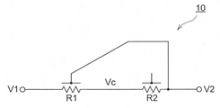
図1は、一実施形態に係る電子回路の回路図を示す。第1抵抗ネットワーク10は、2つの3端子抵抗である第1抵抗R1と、第2抵抗R2と、を備える。3端子抵抗は、サブ端子に印加されている電圧に依存して抵抗値が変化する。以下において、3端子抵抗について、抵抗として接続する端子を第1端子、第2端子とし、上記のサブ端子を第3端子と記載する。以下の説明においては、例えば、第1抵抗R1の抵抗値をR1と記載するが、文脈により、回路素子を表すのか、抵抗値を表すのかは読み分けるものとする。
図1において、第1抵抗R1は、第1端子が外部と接続され、第2端子が第2抵抗R2と直列に接続される。第2抵抗R2は、第1端子が第1抵抗R1の第2端子と接続され、第2端子が外部と接続されるとともに、第1抵抗R1の第3端子と接続される。第1抵抗R1の第1端子と、第2抵抗R2の第2端子とを任意の電子回路内に接続することにより、この第1抵抗ネットワーク10が1つの抵抗として動作する。
この図に示すように、第1抵抗R1は、接続されている第2抵抗R2の端子のうち、自身が接続している端子と反対側、すなわち、遠い側の端子が第3端子に接続される。この図においては、第1抵抗R1と第2抵抗R2の間には他の抵抗が備えられていないが、これらの抵抗間に1又は複数の他の抵抗が備えられていてもよい。すなわち、本実施形態における第1抵抗ネットワーク10は、複数の抵抗を有する抵抗ネットワークに係る回路である。
第1抵抗ネットワーク10は、例えば、入力端子と出力端子とを備え、これらの端子が電圧V1、V2の間に接続されるように回路内に配置される。そして、第1抵抗ネットワーク10は、電圧V1と電圧V2間における抵抗ネットワークとして機能する。
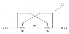
図2は、図1の構成に基づいて実装する第1抵抗ネットワーク10の他の例に係る回路図を示す。第1抵抗R1の接続は、図1に示す例と同様である。この図においては、さらに、第2抵抗R2の第3端子が、第1抵抗R1の第1端子と接続される。
第1抵抗ネットワーク10は、図2に示すように、回路全体としての端子を入れ替えに対して構造が変わらない対称性を有することが望ましい。対称性を有するとは、例えば、電圧V1、V2に接続されている端子を入れ替えても同等の機能を有することをいう。この対称性を担保する上で、第1抵抗R1の抵抗値、第2抵抗R2の抵抗値と、それらの抵抗が同じ特性を有することが好ましい。すなわち、第1抵抗R1と、第2抵抗R2には、同じ抵抗素子が用いられることが望ましい。
上記と同様に、第2抵抗R2の第3端子は、第2抵抗R2からみて、第1抵抗R1の遠い方の端子である第1端子と接続される。このように、第1抵抗R1と第2抵抗R2は、いわゆるたすき掛けの状態で端子同士が接続されていてもよい。
ここで、各図のように接続した場合に、接続された回路に対して抵抗を起因とするどのような信号の歪みが発生するかを計算する。
まず、抵抗値がRの3端子抵抗の第1端子にV1、第2端子にV2、第3端子にVrが印加された場合、この抵抗値は、以下の式(1)のように表される。

ここで、R0は、第3端子の電圧が第1端子と第2端子の電圧の中点である状態における抵抗値であり、kは、抵抗を形成する材料(例えば、ポリシリコン)の実効面積と空乏層とから決定される係数であり典型的には、k ≪ 1を満たす。この式(1)のkの掛かる項が、抵抗の1次歪となる。
図1のように接続される場合、Vr = V2であるので、合成抵抗値Rは、以下のように表される。

一方で、図2のように接続される場合には、抵抗値は、以下のように表される。
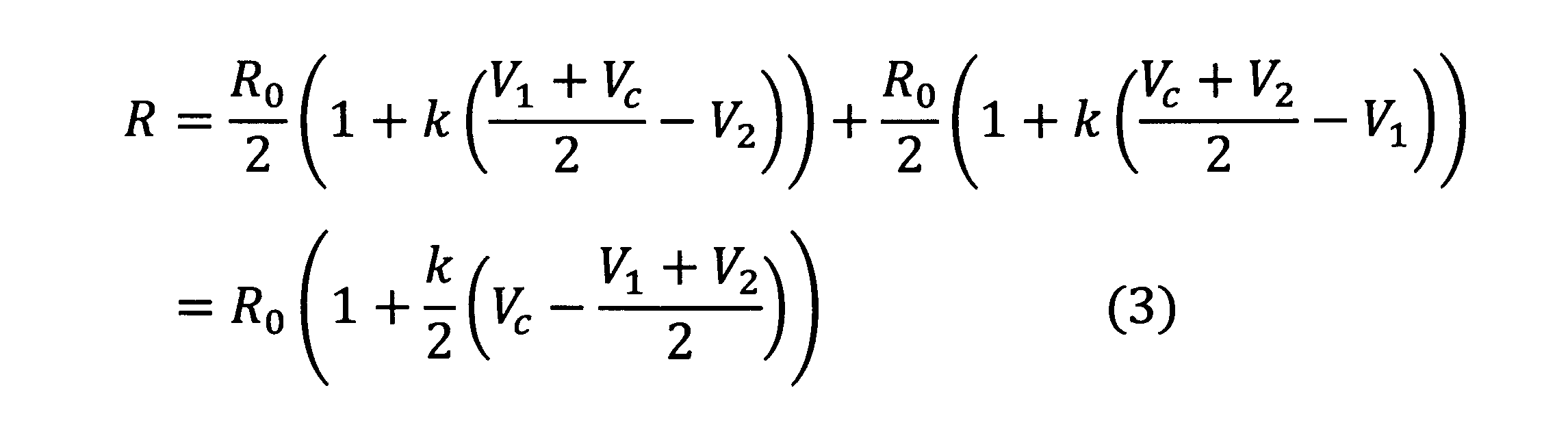
ただし、図に示すように、第1抵抗R1、第2抵抗R2の間の電圧、すなわち、第1抵抗R1の第2端子、第2抵抗R2の第1端子における電位をVcとする。
一方で、VcがV1、V2を第1抵抗R1、第2抵抗R2の抵抗値の比率による分圧で表されることから、R1、R2に対して式(1)を用いると、以下の式(4)が成り立つ。

式(4)をVcについて解くと、式(5)と表される。

ここで、仮にV1 = V2の場合について考えると、Vc = V1 = V2となるので、式(5)中の複号は、プラスと判断することができる。式(5)のVcを式(3)に代入し、k ≪ 1であることから近似すると、合成抵抗値Rについて以下の式が得られる。

この式(6)の関係から、抵抗の電圧依存による歪みは、式(2)では、1次であるのに対して、式(6)では2次となっている。すなわち、3端子抵抗の電圧の1次の歪み成分は、図2のように配置することにより、2次の歪みに変換されていることがわかる。また、k ≪ 1であることから、抵抗の電圧依存性は、図1の場合よりも小さくなっていることがわかる。
また、式(6)は、電圧に対して、上に凸な関数である。このことから、電圧に対して下に凸な2次歪み特性を有する抵抗(ネットワーク)を接続することにより、電圧に対する抵抗の2次歪みの影響を小さくすることができる。
以上のように、本実施形態に係る第1抵抗ネットワーク10によれば、上に凸な2次の電圧に対する特性を有する抵抗を形成することが可能となる。
次に、図2に示した第1抵抗ネットワーク10と組み合わせて用いて抵抗値の電圧に対する2次歪み特性を打ち消す回路について説明する。
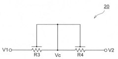
図3は、図2に示した第1抵抗ネットワーク10の電圧による2次歪みを抑制する第2抵抗ネットワークの一例を示す図である。第2抵抗ネットワーク10は、第3抵抗R3と、第4抵抗R4と、を備える。
第3抵抗R3は、第1端子と第3端子とが接続され、第4抵抗R4と直列に接続される。第4抵抗R4は、第2端子と第3端子とが接続され、第1端子が第3抵抗R3の第2端子と接続される。
この合成抵抗値Rは、以下のように表される。
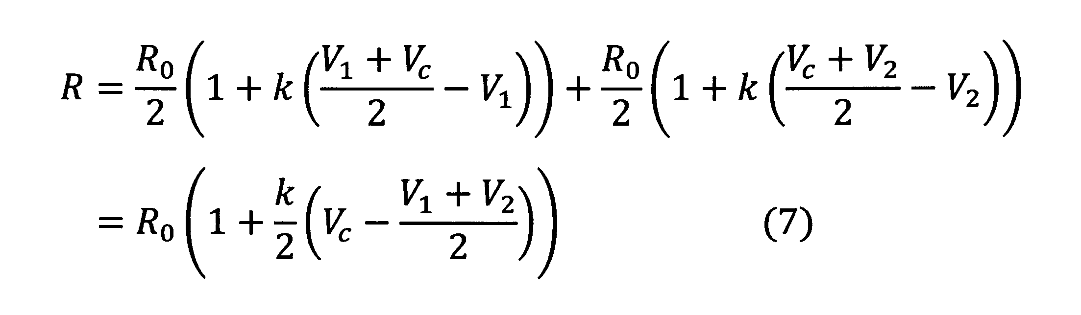
また、Vcは、以下のように表される。
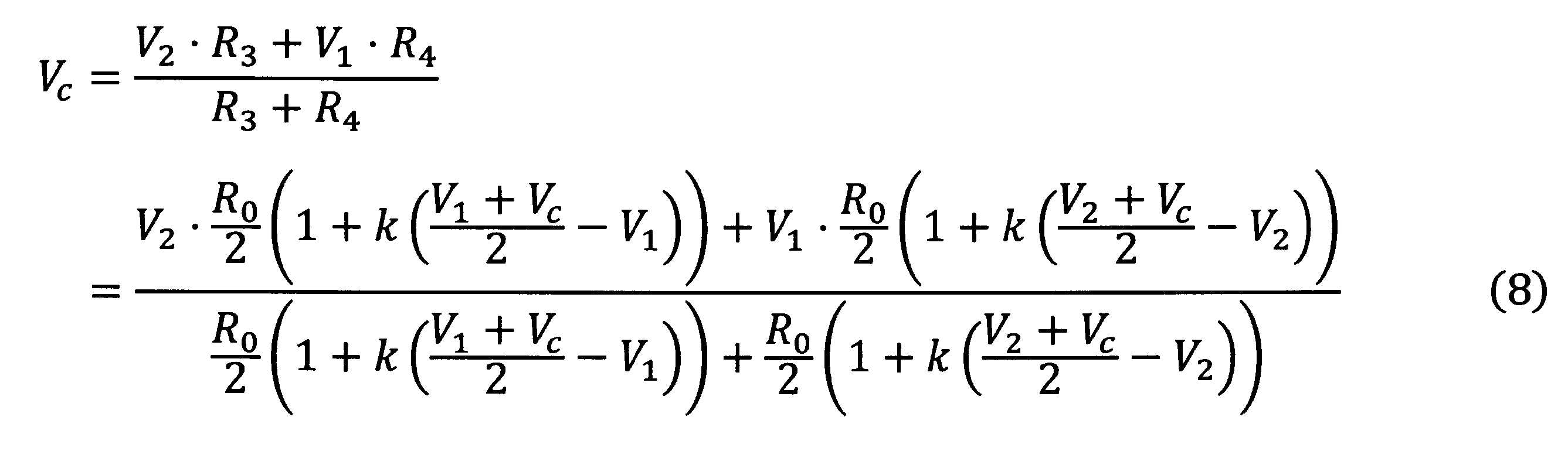
これらの2つの式から、合成抵抗値Rは、上記と同様の式変換をすることにより、以下のように求められる。

この式からわかるよう、図3の第2抵抗ネットワーク20の抵抗値は、下に凸の電圧の2次歪みを有する。
図4は、図3とは異なる構成の図2に示した第1抵抗ネットワーク10の電圧による2次歪みを抑制する第2抵抗ネットワークの一例を示す図である。図3の場合と同様に、第2抵抗ネットワーク10は、第3抵抗R3と、第4抵抗R4と、を備える。
第3抵抗R3は、第2端子と第3端子とが接続され、第4抵抗R4と直列に接続される。第4抵抗R4は、第1端子と第3端子とが接続され、第1端子が第3抵抗R3の第2端子と接続される。
この合成抵抗値Rは、以下のように表される。

また、Vcは、以下のように表される。
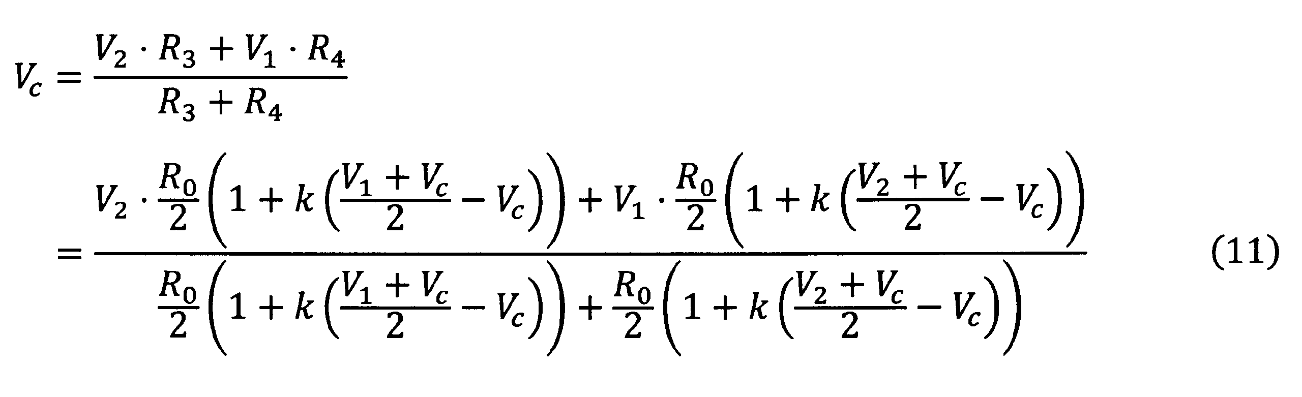
これらの2つの式から、合成抵抗値Rは、上記と同様の式変換をすることにより、以下のように求められる。
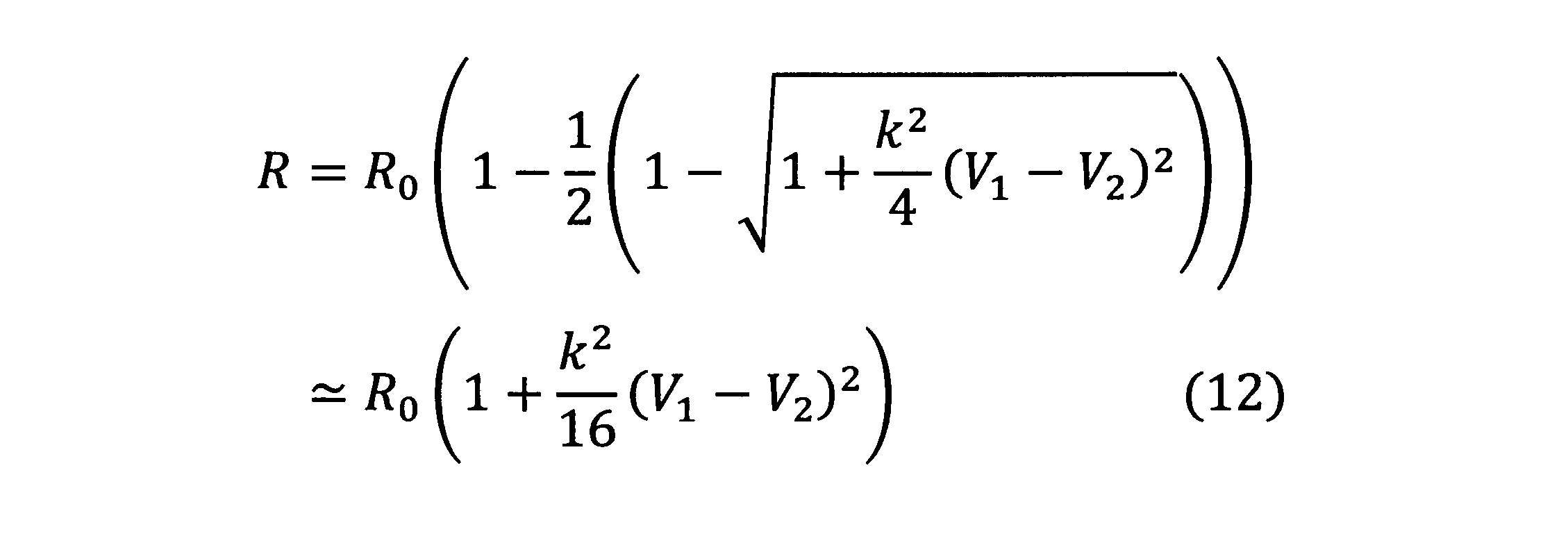
この式からわかるよう、図4の第2抵抗ネットワーク20の抵抗値は、下に凸の電圧の2次歪みを有する。すなわち、図3の場合と同等の特性を有する。
図2に示す第1抵抗ネットワーク10と、図3又は図4に示す第2抵抗ネットワーク20とを組み合わせることにより、全体としての抵抗値の電圧の2次に起因する歪みを小さくすることができる。
以下に、4つの抵抗素子を直列に接続した例をいくつか挙げる。
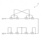
図5は、一実施形態に係る抵抗ネットワークを組み合わせた電子回路を示す図である。例えば、電子回路1は、図2に示す第1抵抗ネットワーク10と、図3に示す第2抵抗ネットワーク20とを直列に接続する。
このように接続することにより、式(6)、式(9)より、電圧による2次歪みが減少するように抵抗を形成することが可能となる。
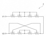
図6は、一実施形態に係る抵抗ネットワークを組み合わせた電子回路を示す図である。例えば、電子回路1は、図2に示す第1抵抗ネットワーク10と、図4に示す第2抵抗ネットワーク20とを直列に接続する。
このように接続することにより、式(6)、式(12)より、電圧による2次歪みが減少するように抵抗を形成することが可能となる。
図5及び図6においては、各抵抗ネットワークを直列に接続したが、直列には限られず、並列に接続してもよい。すなわち、第1抵抗ネットワーク10と第2抵抗ネットワーク20とを並列に組み合わせることにより、電圧に起因する抵抗値の2次歪みを抑制することも可能である。
さらに、抵抗ネットワークが対称性を有するいくつかの例を挙げる。以下に挙げるそれぞれの電子回路1は、
(1)抵抗の接続において対称性を有する、
(2)少なくとも1つ(対称性から少なくとも2つ)の抵抗において、当該抵抗から見て相手方の抵抗において遠い側の端子から第3端子に電圧が印加される、
という共通点を有する。この特性は、例えば、式(2)、式(6)、式(9)、式(12)により表される抵抗の合成として示される。電子回路は、第1抵抗ネットワーク10と、第2抵抗ネットワーク20との双方を備えることが望ましい。
(1)抵抗の接続において対称性を有する、
(2)少なくとも1つ(対称性から少なくとも2つ)の抵抗において、当該抵抗から見て相手方の抵抗において遠い側の端子から第3端子に電圧が印加される、
という共通点を有する。この特性は、例えば、式(2)、式(6)、式(9)、式(12)により表される抵抗の合成として示される。電子回路は、第1抵抗ネットワーク10と、第2抵抗ネットワーク20との双方を備えることが望ましい。
なお、第1ネットワーク10内の抵抗は、同じ特性を備え、第2ネットワーク20内の抵抗は、同じ特性を備える。一方で、第1ネットワーク10内の抵抗と、第2ネットワーク20内の抵抗は、同じ特性を備えなくてもよく、例えば、電圧の2次歪みの上下の凸が打ち消されるような特性を有する組み合わせであってもよい。
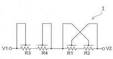
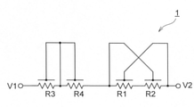
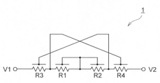
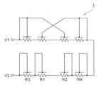
図7は、上記に説明した対称性を有する抵抗の接続例を示すものである。この図7に示す抵抗は、第1抵抗R1と第2抵抗R2とがたすき掛け、第3抵抗R3の第3端子が第1抵抗R1の第3抵抗R3からみた遠い端子である第2端子と接続され、第4抵抗R4の第3端子が第2抵抗R2の第4抵抗R4からみた遠い端子である第1端子と接続される。
電子回路1は、第1抵抗R1、第2抵抗R2に着目すると、図2に示す第1抵抗ネットワーク10を備え、第3抵抗R3、第4抵抗R4に着目すると、図4に示す第2抵抗ネットワーク20を備える。
図8は、上記に説明した対称性を有する抵抗の接続例を示すものである。この図8に示す抵抗は、第1抵抗R1と第2抵抗R2がたすき掛けとなり、第3抵抗R3の第3端子が第1抵抗R1の遠い側の第2端子と接続され、第4抵抗R4の第3端子が第2抵抗R2の遠い側の第1端子と接続される。
電子回路1は、第1抵抗R1、第2抵抗R2に着目すると、図2に示す第1抵抗ネットワーク10を備え、第3抵抗R3、第4抵抗R4に着目すると、図4に示す第2抵抗ネットワーク20を備える。
図9は、上記に説明した対称性を有する抵抗の接続例を示すものである。この図9に示す抵抗は、第1抵抗R1の第3端子が第1端子と接続され、第2抵抗R2の第3端子が第2端子と接続され、第3抵抗R3の第3端子が第1抵抗R1の遠い側の第2端子と接続され、第4抵抗R4の第3端子が第2抵抗R2の遠い側の第1端子と接続される。
図10は、上記に説明した対称性を有する抵抗の接続例を示すものである。この図10に示す抵抗は、第1抵抗R1の第3端子が第2端子と接続され、第2抵抗R2の第3端子が第1端子と接続され、第3抵抗R3の第3端子が第1抵抗R1の遠い側の第2端子と接続され、第4抵抗R4の第3端子が第2抵抗R2の遠い側の第1端子と接続される。
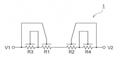
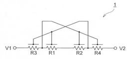
図11は、上記に説明した対称性を有する抵抗の接続例を示すものである。この図11に示す抵抗は、第1抵抗R1と第2抵抗R2とがたすき掛けとなり、第3抵抗R3の第3端子が第1端子と接続され、第4抵抗R4の第3端子が第2端子と接続される。
電子回路1は、第1抵抗R1、第2抵抗R2に着目すると、図2に示す第1抵抗ネットワーク10を備え、第3抵抗R3、第4抵抗R4に着目すると、図3に示す第2抵抗ネットワーク20を備える。
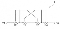
図12は、上記に説明した対称性を有する抵抗の接続例を示すものである。この図12に示す抵抗は、第1抵抗R1と第2抵抗R2とがそれぞれ第3抵抗R3及び第4抵抗R4を介してたすき掛けとなり、第3抵抗R3の第3端子が第1端子と接続され、第4抵抗R4の第3端子が第2抵抗と接続される。
電子回路1は、第1抵抗R1、第2抵抗R2に着目すると、図2に示す第1抵抗ネットワーク10を備え、第3抵抗R3、第4抵抗R4に着目すると、図3に示す第2抵抗ネットワーク20を備える。
図13は、上記に説明した対称性を有する抵抗の接続例を示すものである。この図13に示す抵抗は、第1抵抗R1の第3端子が第3抵抗R3の遠い側の第1端子と接続され、第2抵抗R2の第3端子が第4抵抗R4の遠い側の第2端子と接続され、第3抵抗R3の第3端子が第2端子と接続され、第4抵抗R4の第3端子が第1端子と接続される。
図14は、上記に説明した対称性を有する抵抗の接続例を示すものである。この図14に示す抵抗は、第1抵抗R1と第2抵抗R2とがたすき掛けとなり、第3抵抗R3の第3端子が第2端子と接続され、第4抵抗R4の第3端子が第1端子と接続される。
電子回路1は、第1抵抗R1、第2抵抗R2に着目すると、図2に示す第1抵抗ネットワーク10を備え、第3抵抗R3、第4抵抗R4に着目すると、第1抵抗R1、第2抵抗R2を介して図4に示す第2抵抗ネットワーク20を備える。
図15は、上記に説明した対称性を有する抵抗の接続例を示すものである。この図15に示す抵抗は、第1抵抗R1と第2抵抗R2とがそれぞれ第3抵抗R3及び第4抵抗R4を介してたすき掛けとなり、第3抵抗R3の第3端子が第2端子と接続され、第4抵抗R4の第3端子が第1端子と接続される。
電子回路1は、第1抵抗R1、第2抵抗R2に着目すると、図2に示す第1抵抗ネットワーク10を備え、第3抵抗R3、第4抵抗R4に着目すると、図4に示す第2抵抗ネットワーク20を備える。
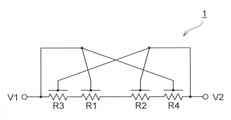
図16は、上記に説明した対称性を有する抵抗の接続例を示すものである。この図16に示す抵抗は、第3抵抗R3と、第1抵抗R1及び第4抵抗R4がたすき掛けとなり、第4抵抗R4と、第2抵抗R2及び第3抵抗R3がたすき掛けとなっている。
電子回路1は、第1抵抗R1、第2抵抗R2に着目すると、図3に示す第2抵抗ネットワーク20を備え、第3抵抗R3、第4抵抗R4に着目すると、図2に示す第1抵抗ネットワーク10を備える。
図17は、上記に説明した対称性を有する抵抗の接続例を示すものである。この図17に示す抵抗は、第1抵抗R1の第3端子と第1端子が接続され、第2抵抗R2の第3端子と第2端子が接続され、第3抵抗R3と、第4抵抗R4がたすき掛けとなっている。
電子回路1は、第1抵抗R1、第2抵抗R2に着目すると、図3に示す第2抵抗ネットワーク20を備え、第3抵抗R3、第4抵抗R4に着目すると、図2に示す第1抵抗ネットワーク10を備える。
図18は、上記に説明した対称性を有する抵抗の接続例を示すものである。この図18に示す抵抗は、第1抵抗R1の第3端子と第2端子が接続され、第2抵抗R2の第3端子と第1端子が接続され、第3抵抗R3と、第4抵抗R4がたすき掛けとなっている。
電子回路1は、第1抵抗R1、第2抵抗R2に着目すると、図4に示す第2抵抗ネットワーク20を備え、第3抵抗R3、第4抵抗R4に着目すると、図2に示す第1抵抗ネットワーク10を備える。
図19は、上記に説明した対称性を有する抵抗の接続例を示すものである。この図19に示す抵抗は、第1抵抗R1と第2抵抗R2、第1抵抗R1と第4抵抗R4、第2抵抗R2と第3抵抗R3、第3抵抗R3と第4抵抗R4がそれぞれたすき掛けとなっている。
図20は、上記に説明した対称性を有する抵抗の接続例を示すものである。この図20に示す抵抗は、第1抵抗R1と第2抵抗R2、第3抵抗R3と第4抵抗R4がそれぞれたすき掛けとなっている。
図21は、上記に説明した対称性を有する抵抗の接続例を示すものである。この図21に示す抵抗は、第1抵抗R1の第3端子が第3抵抗R3の遠い側の第1端子と接続され、第2抵抗R2の第3端子が第4抵抗R4の遠い側の第2端子と接続され、第3抵抗R3の第3端子が第2抵抗R2の遠い側の第2端子と接続され、第4抵抗R4の第3端子が第1抵抗R1の遠い側の第1端子と接続される。
図22は、上記に説明した対称性を有する抵抗の接続例を示すものである。この図22に示す抵抗は、第1抵抗R1の第3端子が第1端子と接続され、第2抵抗R2の第3端子が第2端子と接続され、第3抵抗R3の第3端子が第2抵抗R2の遠い側の第2端子と接続され、第4抵抗R4の第3端子が第1抵抗R1の遠い側の第1端子と接続される。
図23は、上記に説明した対称性を有する抵抗の接続例を示すものである。この図23に示す抵抗は、第1抵抗R1の第3端子が第2端子と接続され、第2抵抗R2の第3端子が第1端子と接続され、第3抵抗R3の第3端子が第2抵抗R2の遠い側の第2端子と接続され、第4抵抗R4の第3端子が第1抵抗R1の遠い側の第1端子と接続される。
図24は、上記に説明した対称性を有する抵抗の接続例を示すものである。この図24に示す抵抗は、第1抵抗R1と第2抵抗R2がたすき掛けとなり、第3抵抗R3の第3端子が第2抵抗R2の遠い側の第2端子と接続され、第4抵抗R4の第3端子が第1抵抗R1の遠い側の第1端子と接続される。
図25は、上記に説明した対称性を有する抵抗の接続例を示すものである。この図25に示す抵抗は、第1抵抗R1と第2抵抗R2が第3抵抗R3、第4抵抗R4を介してたすき掛けとなり、第3抵抗R3の第3端子が第2抵抗R2の遠い側の第2端子と接続され、第4抵抗R4の第3端子が第1抵抗R1の遠い側の第1端子と接続される。
上記に説明した例における簡単な特性について説明する。
図8、図10、図22、図23は、電子回路1全体としてみると、その抵抗値が、電圧に依存して変化する量が大きく、下に凸の特性を有する。図17、図18は、電子回路1全体としてみると、その抵抗値が、電圧に依存して変化する量が大きく、上に凸の特性を有する。
このため、例えば、図8、図10、図22、図23から1つを選択し、図17、図18から1つを選択して、それらの回路を直列又は並列に接続することにより、双方の特性を打ち消すことが可能となる。
図7、図9、図13、図24は、電子回路1全体としてみると、その抵抗値が、電圧に依存して変化する量が小さく、下に凸の特性を有する。図11、図12、図14、図21は、電子回路1全体としてみると、その抵抗値が、電圧に依存して変化する量が小さく、上に凸の特性を有する。
このため、例えば、図7、図9、図13、図24から1つを選択し、図11、図12、図14、図21から1つを選択して、それらの回路を直列又は並列に接続することにより、双方の特性を打ち消すことが可能となる。
なお、いずれの場合においても、歪みを打ち消すように、適切に各抵抗の抵抗値は調整してもよい。
上記に説明した4つの抵抗素子を用いて対称性を持たせて形成した抵抗ネットワークを2つ以上組み合わせてもよい。例えば、以下に2つ組み合わせた例をいくつか挙げる。
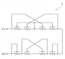
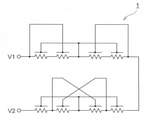
図26は、上記に説明した対称性を有する抵抗群を直列に接続した接続例を示すものである。この図26に示すように、図7の電子回路1と、図11の電子回路1とを組み合わせて新たな電子回路1として抵抗を構成してもよい。
図27は、上記に説明した対称性を有する抵抗群を直列に接続した接続例を示すものである。この図27に示すように、図8の電子回路1と、直列4つに抵抗を接続した対称性を有する抵抗群を組み合わせて新たな電子回路1として抵抗を構成してもよい。
この図27に示す回路は、図8の回路の入力と、図9の回路を変形した回路の出力と、を直列に接続したものである。より具体的には、図9における第1抵抗R1の第3端子を第3抵抗R3の第1端子と接続し、第2抵抗R2の第3端子を第4抵抗R4の第2端子と接続した回路を、図8の回路と直列に接続したものである。
図28は、上記に説明した対称性を有する抵抗群を直列に接続した接続例を示すものである。この図28に示すように、図22の電子回路1と、直列4つに抵抗を接続した対称性を有する抵抗群を組み合わせて新たな電子回路1として抵抗を構成してもよい。
この図28に示す回路は、図22の回路の入力と、図11の回路を変形した回路の出力と、を直列に接続したものである。より具体的には、図11における第1抵抗R1の第3端子を第2端子と接続し、第2抵抗R2の第3端子を第1端子と接続したものである。
図29は、上記に説明した対称性を有する抵抗群を直列に接続した接続例を示すものである。この図29に示すように、図13の電子回路1と、図21の電子回路1とを組み合わせて新たな電子回路1として抵抗を構成してもよい。
図30は、上記に説明した対称性を有する抵抗群を直列に接続した接続例を示すものである。この図30に示すように、図10の電子回路1と、図18の電子回路1とを組み合わせて新たな電子回路1として抵抗を構成してもよい。
図31は、上記に説明した対称性を有する抵抗群を直列に接続した接続例を示すものである。この図31に示すように、図12の電子回路1と、直列4つに抵抗を接続した対称性を有する抵抗群を組み合わせて新たな電子回路1として抵抗を構成してもよい。
この図31に示す回路は、図12の回路の入力と、図9の回路を変形した回路の出力と、を直列に接続したものである。より具体的には、図9における第3抵抗R3の第3端子を第1端子と接続し、第4抵抗R4の第3端子を第2端子と接続したものである。
これらの組み合わせは、一例として示したものであり、上記で説明した他の回路同士を接続してもよい。
以上列挙した電子回路1は、いずれも3端子抵抗において抵抗のサブ端子(第3端子)に印加される電圧値の2次歪みを抑制することが可能となる。このような例によれば、電圧依存による抵抗の歪み特性を、比較器、電圧生成器等の追加の回路を必要とせずに低減することが可能となる。抵抗素子以外の補正回路が必要とならないため、このような補正回路の追加に伴う消費電力の増加を抑制することができる。また、抵抗同士は、同等の特性を有しているものであれば、その極性、材料等は、同じものに限定されるものではない。
このような効果は、上述したように、電子回路1の少なくとも一部に、対称性を有する抵抗の配置を備えることにより実装される。例えば、図7から図31に示すように、電子回路1全体として対称性を備えていてもよいし、図5、図6、及び、図26から図31のように電子回路1が対称性を備える電子回路が複数備えられる構成としてもよい。さらに、抵抗は、本開示においては最大8個であるが、これには限られず、さらに多くの対称性を有する電子回路1が接続されてもよい。
上記のように、抵抗群(抵抗ネットワーク)を直列に接続するとしたが、例えば、図26から図31の例においても、直列ではなく、抵抗ネットワーク同士を並列に接続することにより、歪みを低減させてもよい。
また、いずれの場合においても、対称性を有する抵抗群を複数備える場合には、いずれの抵抗も、その第3端子は、自らが属する他の抵抗の第1端子又は第2端子と接続されていることに留意されたい。
図32は、例えば、信号として正弦振動する電圧を入力した場合におけるいくつかの電子回路1における全体としての抵抗値の振動(電圧に依存して変化する量)を示す図である。実線は、図6に示す電子回路1の抵抗値、点線は、図2に示す電子回路1の抵抗値、破線は、図3又は図4に示す電子回路1の抵抗値を示す。
図6に示す電子回路1の抵抗値は、このグラフを見てわかるように、2つの抵抗を備える場合と比較して、その電圧に依存して変化する量を非常に小さくできることがわかる。例えば、一シミュレーションによる例では、同じ電圧、同じ抵抗値を有する素子を用いる場合には、点線の振幅は468.8mΩ、破線の振幅は155.8mΩであるのに対して、実線の振幅(変化量)は667nΩと、約20万分の1から70万分の1程度の振幅(変化量)となる。また、上述した各組み合わせによれば、これよりもさらに振幅(変化量)の値を小さくすることが可能となる。
このように、本実施形態に係る電子回路1によれば、3端子抵抗におけるサブ端子に、少なくとも、当該3端子抵抗と直列に接続される他の抵抗の遠い側の端子における電圧を印加する構成を有することにより、電圧の変動による抵抗の2次の歪みを補正することが可能となる。
本実施形態における電子回路1に備えられる第1抵抗ネットワーク10の基本形である図2に示す回路図のレイアウト例について説明する。
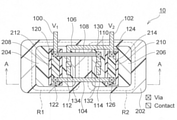
図33は、図2に示す回路図のレイアウトを示す平面図である。例えば、第1抵抗R1、第2抵抗R2は、半導体基板上に形成された抵抗である。
図34は、図33のA-A断面図である。なお、以下のレイアウト、断面等は、一例であり、本開示における形態は、これらに限られるものではない。また、以下の導電型は、一例として記載しているだけであり、導電型ものこれらに限定されるものではない。
第1抵抗R1、第2抵抗R2は、ともに、半導体基板上に生成されてもよい。例えば、半導体基板は、P型の基板200である。半導体基板上に、N型のウェル202を形成し、N型のウェル上に、P型のウェル204、206を形成する。このウェル領域上に抵抗が形成される。例えば、P型のウェル204、206は、メタルであってもよい。
P型のウェル領域204上には、絶縁膜208が形成され、この絶縁膜208上にポリシリコン212が形成され、このポリシリコン212が抵抗の役割を果たす。同様に、ウェル206上には、絶縁膜210が形成され、この絶縁膜210上にポリシリコン214が形成され、このポリシリコン214が抵抗として機能する。
このポリシリコン及びウェル領域と外部との接続について説明する。
V1の電圧が印加される端子、すなわち、上述した入力端子(又は出力端子)として、導線100が備えられる。同様に、V2の電圧が印加される端子、すなわち上述した出力端子(又は入力端子)として、導線102が備えられる。
導線100に印加された電圧は、ビア120(第1端子)を介してポリシリコン212へと印加される。そして、このポリシリコン212は、異なる領域においてビア122(第2端子)を介して導線104と接続される。
導線104は、他方の端部において、ビア126(第1端子)を介してポリシリコン214と接続される。ポリシリコン214は、異なる領域においてビア124(第2端子)を介して導線102、すなわち、出力端子と接続する。このように、ポリシリコン212、214により、直列に接続された抵抗が形成される。
図2に示すように、入力端子と出力端子は、抵抗の第3端子に接続される。この接続について説明する。
導線100は、ビア100を介して、上記とは異なる導線108と接続される。導線108は、第2抵抗R2上において、ビア130、導線110及びコンタクト132を介して、ウェル206上の電極114(第3端子)へと接続する。この電極114により、ウェル206に電圧が印加され、抵抗値が変動する。
同様に、導線102は、第1抵抗R1上で導線106及びコンタクト134を介して、電極112(第3端子)へと接続する。この電極112により、ウェル204に電圧が印加され抵抗値が変動する。
このように、第1抵抗R1、第2抵抗R2は、それぞれにウェル領域を有する抵抗として、同一の半導体基板上に形成されてもよい。そして、このように接続することにより、第1抵抗R1の第1端子と第2抵抗R2の第3端子に同じ電圧を印加し、第2抵抗R2の第2端子と第1抵抗R1の第3端子に同じ電圧を印加することができる。
図35、図36は、この基板上の別の例を示す。図35に示すように、第1抵抗R1を同一のウェル上で分割して配置してもよい。第2抵抗R2についても同様である。
図36に示すように、第1抵抗R1を異なるウェル上で分割して配置してもよい。第2抵抗R2についても同様である。
前述した実施形態は、以下のような形態としてもよい。
(1)
第1端子と第2端子間で電圧に対する抵抗の構成を有し、前記第1端子が、直接的に又は間接的に入力と接続される、第1抵抗と、
第1端子と第2端子間で電圧に対する抵抗の構成を有し、前記第1端子が、直接的に又は間接的に前記第1抵抗の第2端子と接続され、第2端子が出力と接続される、第2抵抗と、
を備え、
前記第1抵抗の抵抗値を電圧により変動させる第3端子に、前記第2抵抗の前記第2端子が、直接的に又は間接的に接続される、
電子回路。
第1端子と第2端子間で電圧に対する抵抗の構成を有し、前記第1端子が、直接的に又は間接的に入力と接続される、第1抵抗と、
第1端子と第2端子間で電圧に対する抵抗の構成を有し、前記第1端子が、直接的に又は間接的に前記第1抵抗の第2端子と接続され、第2端子が出力と接続される、第2抵抗と、
を備え、
前記第1抵抗の抵抗値を電圧により変動させる第3端子に、前記第2抵抗の前記第2端子が、直接的に又は間接的に接続される、
電子回路。
(2)
前記第2抵抗の抵抗値を電圧により変動させる第3端子に、前記第1抵抗の前記第1端子が接続される、
電子回路。
前記第2抵抗の抵抗値を電圧により変動させる第3端子に、前記第1抵抗の前記第1端子が接続される、
電子回路。
(3)
前記第1抵抗の前記第1端子を前記出力に接続し、前記第2抵抗の前記第2端子を前記入力に接続した場合においても同じ構成となる対称性を有する、
(1)又は(2)に記載の電子回路。
前記第1抵抗の前記第1端子を前記出力に接続し、前記第2抵抗の前記第2端子を前記入力に接続した場合においても同じ構成となる対称性を有する、
(1)又は(2)に記載の電子回路。
(4)
第1端子、第2端子、第3端子を有する第3抵抗と、
第1端子、第2端子、第3端子を有する第4抵抗と、
をさらに備え、
前記第1抵抗と前記第2抵抗により形成される、第1抵抗群と、
前記第3抵抗と前記第4抵抗により形成され、前記第3抵抗の前記第2端子と、前記第4抵抗の前記第1端子が少なくとも接続され、対称性を有し、前記第1抵抗群とは異なる接続の構成を有する、第2抵抗群とにおいて、
前記第1抵抗群と、前記第2抵抗群が、直列、又は、並列に接続され、
前記第1抵抗群及び前記第2抵抗群に属するいずれの抵抗においても、前記第3端子は、自身が属する抵抗群の他の抵抗の前記第1端子又は前記第2端子と接続される、
(3)に記載の電子回路。
第1端子、第2端子、第3端子を有する第3抵抗と、
第1端子、第2端子、第3端子を有する第4抵抗と、
をさらに備え、
前記第1抵抗と前記第2抵抗により形成される、第1抵抗群と、
前記第3抵抗と前記第4抵抗により形成され、前記第3抵抗の前記第2端子と、前記第4抵抗の前記第1端子が少なくとも接続され、対称性を有し、前記第1抵抗群とは異なる接続の構成を有する、第2抵抗群とにおいて、
前記第1抵抗群と、前記第2抵抗群が、直列、又は、並列に接続され、
前記第1抵抗群及び前記第2抵抗群に属するいずれの抵抗においても、前記第3端子は、自身が属する抵抗群の他の抵抗の前記第1端子又は前記第2端子と接続される、
(3)に記載の電子回路。
(5)
第1端子、第2端子、第3端子を有し、前記第2端子が前記第1抵抗の前記第1端子と接続される、第3抵抗と、
第1端子、第2端子、第3端子を有し、前記第1端子が前記第2抵抗の前記第2端子と接続される、第4抵抗と、
をさらに備える、(1)から(3)のいずれかに記載の電子回路。
第1端子、第2端子、第3端子を有し、前記第2端子が前記第1抵抗の前記第1端子と接続される、第3抵抗と、
第1端子、第2端子、第3端子を有し、前記第1端子が前記第2抵抗の前記第2端子と接続される、第4抵抗と、
をさらに備える、(1)から(3)のいずれかに記載の電子回路。
(6)
前記第3抵抗、前記第1抵抗、前記第2抵抗、前記第4抵抗の順番で対称性を有する、
(5)に記載の電子機器。
前記第3抵抗、前記第1抵抗、前記第2抵抗、前記第4抵抗の順番で対称性を有する、
(5)に記載の電子機器。
(7)
前記第3抵抗、前記第1抵抗、前記第2抵抗、前記第4抵抗を有する第1抵抗群と、
対称性を有する他の抵抗群である第2抵抗群と、において、
前記第1抵抗群と、前記第2抵抗群が、直列、又は、並列に接続され、
前記第1抵抗群及び前記第2抵抗群に属するいずれの抵抗においても、前記第3端子は、自身が属する抵抗群の他の抵抗の前記第1端子又は前記第2端子と接続される、
(6)に記載の電子回路。
前記第3抵抗、前記第1抵抗、前記第2抵抗、前記第4抵抗を有する第1抵抗群と、
対称性を有する他の抵抗群である第2抵抗群と、において、
前記第1抵抗群と、前記第2抵抗群が、直列、又は、並列に接続され、
前記第1抵抗群及び前記第2抵抗群に属するいずれの抵抗においても、前記第3端子は、自身が属する抵抗群の他の抵抗の前記第1端子又は前記第2端子と接続される、
(6)に記載の電子回路。
本開示の態様は、前述した実施形態に限定されるものではなく、想到しうる種々の変形も含むものであり、本開示の効果も前述の内容に限定されるものではない。各実施形態における構成要素は、適切に組み合わされて適用されてもよい。すなわち、特許請求の範囲に規定された内容及びその均等物から導き出される本開示の概念的な思想と趣旨を逸脱しない範囲で種々の追加、変更及び部分的削除が可能である。
1:電子回路、
10:第1抵抗ネットワーク、
20:第2抵抗ネットワーク、
R1、R2、R3、R4:3端子抵抗
10:第1抵抗ネットワーク、
20:第2抵抗ネットワーク、
R1、R2、R3、R4:3端子抵抗
Claims (7)
- 第1端子と第2端子間で電圧に対する抵抗の構成を有し、前記第1端子が、直接的に又は間接的に入力と接続される、第1抵抗と、
第1端子と第2端子間で電圧に対する抵抗の構成を有し、前記第1端子が、直接的に又は間接的に前記第1抵抗の第2端子と接続され、第2端子が出力と接続される、第2抵抗と、
を備え、
前記第1抵抗の抵抗値を電圧により変動させる第3端子に、前記第2抵抗の前記第2端子が、直接的に又は間接的に接続される、
電子回路。 - 前記第2抵抗の抵抗値を電圧により変動させる第3端子に、前記第1抵抗の前記第1端子が接続される、
請求項1に記載の電子回路。 - 前記第1抵抗の前記第1端子を前記出力に接続し、前記第2抵抗の前記第2端子を前記入力に接続した場合においても同じ構成となる対称性を有する、
請求項1に記載の電子回路。 - 第1端子、第2端子、第3端子を有する第3抵抗と、
第1端子、第2端子、第3端子を有する第4抵抗と、
をさらに備え、
前記第1抵抗と前記第2抵抗により形成される、第1抵抗群と、
前記第3抵抗と前記第4抵抗により形成され、前記第3抵抗の前記第2端子と、前記第4抵抗の前記第1端子が少なくとも直接的又は間接的に接続され、対称性を有し、前記第1抵抗群とは異なる接続の構成を有する、第2抵抗群とにおいて、
前記第1抵抗群と、前記第2抵抗群が、直列、又は、並列に接続され、
前記第1抵抗群及び前記第2抵抗群に属するいずれの抵抗においても、前記第3端子は、自身が属する抵抗群の他の抵抗の前記第1端子又は前記第2端子と接続される、
請求項3に記載の電子回路。 - 第1端子、第2端子、第3端子を有し、前記第2端子が前記第1抵抗の前記第1端子と接続される、第3抵抗と、
第1端子、第2端子、第3端子を有し、前記第1端子が前記第2抵抗の前記第2端子と接続される、第4抵抗と、
をさらに備える、請求項1に記載の電子回路。 - 前記第3抵抗、前記第1抵抗、前記第2抵抗、前記第4抵抗の順番で対称性を有する、
請求項5に記載の電子機器。 - 前記第3抵抗、前記第1抵抗、前記第2抵抗、前記第4抵抗を有する第1抵抗群と、
対称性を有する他の抵抗群である第2抵抗群と、において、
前記第1抵抗群と、前記第2抵抗群が、直列、又は、並列に接続され、
前記第1抵抗群及び前記第2抵抗群に属するいずれの抵抗においても、前記第3端子は、自身が属する抵抗群の他の抵抗の前記第1端子又は前記第2端子と接続される、
請求項6に記載の電子回路。
Priority Applications (1)
| Application Number | Priority Date | Filing Date | Title |
|---|---|---|---|
| US18/004,911 US20230246622A1 (en) | 2020-07-20 | 2021-06-23 | Electronic circuit |
Applications Claiming Priority (2)
| Application Number | Priority Date | Filing Date | Title |
|---|---|---|---|
| JP2020123728A JP2022020311A (ja) | 2020-07-20 | 2020-07-20 | 電子回路 |
| JP2020-123728 | 2020-07-20 |
Publications (1)
| Publication Number | Publication Date |
|---|---|
| WO2022019042A1 true WO2022019042A1 (ja) | 2022-01-27 |
Family
ID=79729434
Family Applications (1)
| Application Number | Title | Priority Date | Filing Date |
|---|---|---|---|
| PCT/JP2021/023753 Ceased WO2022019042A1 (ja) | 2020-07-20 | 2021-06-23 | 電子回路 |
Country Status (3)
| Country | Link |
|---|---|
| US (1) | US20230246622A1 (ja) |
| JP (1) | JP2022020311A (ja) |
| WO (1) | WO2022019042A1 (ja) |
Citations (3)
| Publication number | Priority date | Publication date | Assignee | Title |
|---|---|---|---|---|
| JP2010109233A (ja) * | 2008-10-31 | 2010-05-13 | Renesas Technology Corp | 半導体装置 |
| JP2013187470A (ja) * | 2012-03-09 | 2013-09-19 | Asahi Kasei Electronics Co Ltd | 非反転バッファ回路 |
| JP2013197487A (ja) * | 2012-03-22 | 2013-09-30 | Asahi Kasei Electronics Co Ltd | 反転バッファ回路および電子ボリューム回路 |
Family Cites Families (4)
| Publication number | Priority date | Publication date | Assignee | Title |
|---|---|---|---|---|
| JP4982921B2 (ja) * | 2001-03-05 | 2012-07-25 | ルネサスエレクトロニクス株式会社 | 半導体装置及びその製造方法 |
| EP2602817A1 (en) * | 2011-12-05 | 2013-06-12 | Nxp B.V. | Integrated circuit and IC manufacturing method |
| US9553139B2 (en) * | 2015-01-30 | 2017-01-24 | Semiconductor Components Industries, Llc | Semiconductor component and method of manufacture |
| US10651170B2 (en) * | 2017-07-11 | 2020-05-12 | Taiwan Semiconductor Manufacturing Co., Ltd. | Isolated wells for resistor devices |
-
2020
- 2020-07-20 JP JP2020123728A patent/JP2022020311A/ja active Pending
-
2021
- 2021-06-23 US US18/004,911 patent/US20230246622A1/en not_active Abandoned
- 2021-06-23 WO PCT/JP2021/023753 patent/WO2022019042A1/ja not_active Ceased
Patent Citations (3)
| Publication number | Priority date | Publication date | Assignee | Title |
|---|---|---|---|---|
| JP2010109233A (ja) * | 2008-10-31 | 2010-05-13 | Renesas Technology Corp | 半導体装置 |
| JP2013187470A (ja) * | 2012-03-09 | 2013-09-19 | Asahi Kasei Electronics Co Ltd | 非反転バッファ回路 |
| JP2013197487A (ja) * | 2012-03-22 | 2013-09-30 | Asahi Kasei Electronics Co Ltd | 反転バッファ回路および電子ボリューム回路 |
Also Published As
| Publication number | Publication date |
|---|---|
| US20230246622A1 (en) | 2023-08-03 |
| JP2022020311A (ja) | 2022-02-01 |
Similar Documents
| Publication | Publication Date | Title |
|---|---|---|
| USRE46486E1 (en) | Semiconductor pressure sensor | |
| US7388737B2 (en) | Multilayer capacitor and method of adjusting equivalent series resistance of multilayer capacitor | |
| US9147527B2 (en) | Variable capacity composite component | |
| US20050161725A1 (en) | Semiconductor component comprising an integrated latticed capacitance structure | |
| JP2008226998A (ja) | 半導体集積回路 | |
| US7298604B2 (en) | Multilayer capacitor and method of adjusting equivalent series resistance of multilayer capacitor | |
| JPWO2016136411A1 (ja) | キャパシタおよび電子機器 | |
| WO2022019042A1 (ja) | 電子回路 | |
| CN111309088B (zh) | 基准电压产生装置 | |
| JPH0645109A (ja) | 積層型チップバリスタ | |
| TWI642270B (zh) | 放大電路 | |
| JP7759593B2 (ja) | バリスタ部品 | |
| KR20040015673A (ko) | 반도체 장치 | |
| JP7584997B2 (ja) | 電子モジュール及び電子機器 | |
| US10425043B1 (en) | Operational amplifier with constant transconductance bias circuit and method using the same | |
| JP5002468B2 (ja) | 半導体圧力センサ | |
| US20060091443A1 (en) | Composite capacitor | |
| JP2005151219A (ja) | ポリフェーズフィルタ | |
| JP4650807B2 (ja) | 積層コンデンサ | |
| JP7434410B2 (ja) | 電圧増幅回路装置及び電圧印加回路 | |
| CN115244637B (zh) | 电容器组件 | |
| JP2005516420A (ja) | 電子装置 | |
| US20240105365A1 (en) | Multilayer varistor | |
| US20220200598A1 (en) | Level Shifter Including Dummy Circuit and Method of Manufacturing the Same | |
| CN116895652A (zh) | 半导体装置 |
Legal Events
| Date | Code | Title | Description |
|---|---|---|---|
| 121 | Ep: the epo has been informed by wipo that ep was designated in this application |
Ref document number: 21846616 Country of ref document: EP Kind code of ref document: A1 |
|
| NENP | Non-entry into the national phase |
Ref country code: DE |
|
| 122 | Ep: pct application non-entry in european phase |
Ref document number: 21846616 Country of ref document: EP Kind code of ref document: A1 |