WO2022019033A1 - 電子機器、および電気音響変換装置 - Google Patents
電子機器、および電気音響変換装置 Download PDFInfo
- Publication number
- WO2022019033A1 WO2022019033A1 PCT/JP2021/023639 JP2021023639W WO2022019033A1 WO 2022019033 A1 WO2022019033 A1 WO 2022019033A1 JP 2021023639 W JP2021023639 W JP 2021023639W WO 2022019033 A1 WO2022019033 A1 WO 2022019033A1
- Authority
- WO
- WIPO (PCT)
- Prior art keywords
- pulse signal
- signal
- circuit
- switching element
- terminal
- Prior art date
- Legal status (The legal status is an assumption and is not a legal conclusion. Google has not performed a legal analysis and makes no representation as to the accuracy of the status listed.)
- Ceased
Links
Images




Classifications
-
- H—ELECTRICITY
- H03—ELECTRONIC CIRCUITRY
- H03F—AMPLIFIERS
- H03F1/00—Details of amplifiers with only discharge tubes, only semiconductor devices or only unspecified devices as amplifying elements
- H03F1/26—Modifications of amplifiers to reduce influence of noise generated by amplifying elements
-
- H—ELECTRICITY
- H03—ELECTRONIC CIRCUITRY
- H03F—AMPLIFIERS
- H03F3/00—Amplifiers with only discharge tubes or only semiconductor devices as amplifying elements
- H03F3/181—Low-frequency amplifiers, e.g. audio preamplifiers
- H03F3/183—Low-frequency amplifiers, e.g. audio preamplifiers with semiconductor devices only
- H03F3/185—Low-frequency amplifiers, e.g. audio preamplifiers with semiconductor devices only with field-effect devices
-
- H—ELECTRICITY
- H03—ELECTRONIC CIRCUITRY
- H03F—AMPLIFIERS
- H03F3/00—Amplifiers with only discharge tubes or only semiconductor devices as amplifying elements
- H03F3/20—Power amplifiers, e.g. Class B amplifiers, Class C amplifiers
- H03F3/21—Power amplifiers, e.g. Class B amplifiers, Class C amplifiers with semiconductor devices only
- H03F3/217—Class D power amplifiers; Switching amplifiers
- H03F3/2175—Class D power amplifiers; Switching amplifiers using analogue-digital or digital-analogue conversion
-
- H—ELECTRICITY
- H03—ELECTRONIC CIRCUITRY
- H03F—AMPLIFIERS
- H03F3/00—Amplifiers with only discharge tubes or only semiconductor devices as amplifying elements
- H03F3/20—Power amplifiers, e.g. Class B amplifiers, Class C amplifiers
- H03F3/21—Power amplifiers, e.g. Class B amplifiers, Class C amplifiers with semiconductor devices only
- H03F3/217—Class D power amplifiers; Switching amplifiers
- H03F3/2178—Class D power amplifiers; Switching amplifiers using more than one switch or switching amplifier in parallel or in series
-
- H—ELECTRICITY
- H04—ELECTRIC COMMUNICATION TECHNIQUE
- H04B—TRANSMISSION
- H04B1/00—Details of transmission systems, not covered by a single one of groups H04B3/00 - H04B13/00; Details of transmission systems not characterised by the medium used for transmission
- H04B1/02—Transmitters
- H04B1/04—Circuits
-
- H—ELECTRICITY
- H04—ELECTRIC COMMUNICATION TECHNIQUE
- H04B—TRANSMISSION
- H04B1/00—Details of transmission systems, not covered by a single one of groups H04B3/00 - H04B13/00; Details of transmission systems not characterised by the medium used for transmission
- H04B1/02—Transmitters
- H04B1/04—Circuits
- H04B1/0475—Circuits with means for limiting noise, interference or distortion
-
- H—ELECTRICITY
- H04—ELECTRIC COMMUNICATION TECHNIQUE
- H04B—TRANSMISSION
- H04B1/00—Details of transmission systems, not covered by a single one of groups H04B3/00 - H04B13/00; Details of transmission systems not characterised by the medium used for transmission
- H04B1/69—Spread spectrum techniques
- H04B1/7163—Spread spectrum techniques using impulse radio
- H04B1/71637—Receiver aspects
-
- H—ELECTRICITY
- H04—ELECTRIC COMMUNICATION TECHNIQUE
- H04R—LOUDSPEAKERS, MICROPHONES, GRAMOPHONE PICK-UPS OR LIKE ACOUSTIC ELECTROMECHANICAL TRANSDUCERS; ELECTRIC HEARING AIDS; PUBLIC ADDRESS SYSTEMS
- H04R3/00—Circuits for transducers
-
- H—ELECTRICITY
- H03—ELECTRONIC CIRCUITRY
- H03F—AMPLIFIERS
- H03F2200/00—Indexing scheme relating to amplifiers
- H03F2200/03—Indexing scheme relating to amplifiers the amplifier being designed for audio applications
-
- H—ELECTRICITY
- H03—ELECTRONIC CIRCUITRY
- H03F—AMPLIFIERS
- H03F2200/00—Indexing scheme relating to amplifiers
- H03F2200/372—Noise reduction and elimination in amplifier
Definitions
- This disclosure relates to electronic devices and electroacoustic converters.
- Electronic devices are used to amplify weak audio signals and drive electro-acoustic conversion elements such as speakers and headphones.
- terminals such as smartphones also perform wireless communication while listening to voice based on voice signals.
- the noise generated by the electroacoustic conversion may interfere with the communication frequency of the transmitted / received signal.
- One aspect of the present disclosure provides an electronic device capable of suppressing noise and an electroacoustic conversion device.
- a voltage based on a DC power supply is applied to one end of an electroacoustic converter in response to a first pulse signal, and the electroacoustic converter responds to a second pulse signal.
- a switching element unit that applies a voltage based on the DC power supply to the other end of the A delay circuit that causes a delay based on the communication frequency with respect to at least one of the first pulse signal and the second pulse signal.
- Electronic devices are provided.
- the delay circuit may generate a delay time based on the cycle of the communication frequency.
- the delay time may be half of the cycle of the communication frequency.
- the switching element unit is The first and second switching elements connected in series to the DC power supply, It has a third and fourth switching element connected in series to the DC power supply, and has.
- One end of the electroacoustic transducer may be connected to the connection point of the first and second switching elements, and the other end may be connected to the connection point of the third and fourth switching elements.
- the first switching element is turned on and off by the first pulse signal
- the second switching element is turned off when the first switching element is turned on
- the second switching element is turned on when the first switching element is turned off.
- 1st gate control circuit and The third switching element is turned on and off by the second pulse signal, the fourth switching element is turned off when the third switching element is turned on, and the third switching element is turned on when the third switching element is turned off.
- a third gate control circuit may be further provided.
- the first pulse signal and the pulse generator for generating the second pulse signal are further provided, and the first pulse signal is a pulse signal having a duty ratio according to the level of the voice signal, and the first pulse signal is described.
- the pulse signal of 2 may be a pulse signal having a duty ratio according to the level of the voice signal.
- the delay circuit causes a delay of the first delay time based on the cycle of the communication frequency, the first pulse signal, and a delay of the second delay time based on the cycle of the communication frequency. 2 pulse signals may be generated.
- the delay circuit is A first flip-flop circuit in which the pulse signal is input to the D terminal, a clock signal based on the cycle of the communication frequency is input to the clock terminal, and the first pulse signal is output from the Q terminal.
- the delay circuit is The first delay circuit to which the pulse signal is input and The second delay circuit to which the output signal of the first delay circuit is input and The pulse signal, the exclusive OR circuit to which the output signal of the second delay circuit is input, and An ethical AND circuit in which the output signal of the exclusive OR circuit and the clock signal based on the cycle of the communication frequency are input, and A first flip-flop circuit in which the output signal of the first delay circuit is input to the D terminal, the output signal of the ethical product circuit is input to the clock terminal, and the first pulse signal is output from the Q terminal. It has a second flip-flop circuit in which the first pulse signal is input to the D terminal, the output signal of the ethical product circuit is input to the clock terminal, and the second pulse signal is output from the Q terminal. May be good.
- the delay circuit is The first delay circuit to which the pulse signal is input and The second delay circuit to which the output signal of the first delay circuit is input and The pulse signal, the exclusive OR circuit to which the output signal of the second delay circuit is input, and An ethical AND circuit in which the output signal of the exclusive OR circuit and the clock signal based on the cycle of the communication frequency are input, and A first flip-flop circuit in which the output signal of the first delay circuit is input to the D terminal, the output signal of the ethical product circuit is input to the clock terminal, and the first pulse signal is output from the Q terminal. It has a second flip-flop circuit in which the first pulse signal is input to the D terminal, the output signal of the ethical product circuit is input to the clock terminal, and the second pulse signal is output from the Q terminal. May be good.
- the delay circuit may be driven based on the signal of the reference frequency.
- the reference frequency output by the frequency synthesizer may be switched according to the time zone.
- a communication device that performs at least one of transmission and reception at the communication frequency based on the reference frequency may be further provided.
- a communication device that performs at least one of transmission and reception at the communication frequency and a communication device that performs at least one of transmission and reception are used. It is equipped with a switching element unit that applies a voltage based on a DC power supply to an electroacoustic converter in response to two pulse signals based on an audio signal. An electronic device is provided in which at least one of the two pulse signals is delayed with a period based on the communication frequency.
- An electroacoustic converter including the above electronic device and the electroacoustic converter may be provided.
- the figure which shows an example of the structure of the electroacoustic conversion apparatus which concerns on this embodiment The figure which shows the relationship between 1 pulse signal, 2nd pulse signal, and a speaker applied voltage.
- the figure explaining the reduction of the noise component in FIG. The figure which shows an example of the structure of the electroacoustic conversion apparatus which concerns on 2nd Embodiment.
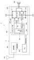
- FIG. 1 is a diagram showing an example of the configuration of the electroacoustic conversion device 1 according to the present embodiment.
- the electroacoustic conversion device 1 is a device capable of wireless communication and acoustic conversion of an audio signal Sm.
- the electroacoustic conversion device 1 includes an electronic device 2, an antenna 100, and headphones 500.
- the electronic device 2 includes a communication device 200, a frequency synthesizer 300, and a headphone amplifier unit 400.
- the antenna 100 receives the reception signal of the radio frequency and transmits the transmission signal of the radio frequency.
- the communication device 200 is, for example, a BT receiver, and after amplifying a signal corresponding to a communication frequency fc in the 2.4 Ghz band received by the antenna 100, it is converted into a digital signal.
- the BT receiver can support BLE specialized for power saving applications of Bluetooth (registered trademark).
- the communication device 200 according to the present embodiment is, for example, a BT receiver, but is not limited thereto.
- the communication device 200 may be a GNSS transceiver.
- the frequency synthesizer 300 is a phased lock loop (PLL) circuit that loop-controls the oscillation frequency fc of the communication device 200.
- the frequency synthesizer 300 generates a reference frequency signal having a frequency of 2 ⁇ fc corresponding to, for example, twice the communication frequency fc, and supplies the frequency signal of the frequency fc to the communication device 200.
- the frequency synthesizer 300 generates a reference frequency signal based on, for example, a frequency band signal of a transmission / reception signal.
- the frequency band signal is Bluetooth compliant.
- the frequency of 2.402 to 2.480 [GHz] is divided into 79. That is, communication is performed using any of the frequencies of 2.402 [GHz], 2.403 [GHz], 2.404 [GHz], ..., 2.480 [GHz].
- the communication device 200 switches (hopping) the frequency band used by the frequency synthesizer 300 every hour.
- the headphone amplifier unit 400 is, for example, a filterless class D amplifier.
- the headphone amplifier unit 400 includes a pulse generator 402, a delay circuit 404, and a switching element unit 405.
- the switching element unit 405 includes a first gate control circuit 406, first switching elements 408 and 410, a second gate control circuit 412, and a second switching element 414 and 416.
- the switching elements 408, 410, 414, 416 connected in full bridge are turned on by a pulse signal (PWM signal) of a predetermined frequency whose pulse width is modulated according to the signal level of the input audio signal Sm. , Off-switching.
- PWM signal pulse signal
- the headphones 500 electroacoustic converter
- the pulse generator 402 generates a first pulse signal (Sp signal) and a second pulse signal (Sn signal) according to the audio signal Sm.
- the first pulse signal is a pulse signal having a duty ratio corresponding to the level of the voice signal Sm
- the second pulse signal is a pulse signal having a duty ratio corresponding to the level of the voice signal Sm.
- the delay circuit 404 according to the present embodiment delays the second pulse signal, but is not limited thereto. For example, the first pulse signal may be delayed. Details of the delay circuit 404 will be described later.
- the signal based on the communication frequency fc is supplied from the frequency synthesizer 300. Therefore, for example, even when the frequency band used by the frequency synthesizer 300 is switched (hopping) every time, it is possible to cause a delay based on the communication frequency fc in the second pulse signal.
- FIG. 2 is a diagram showing the relationship between the first pulse signal generated by the pulse generator 402, the second pulse signal, and the speaker applied voltage.
- A shows the first pulse signal
- B shows the second pulse signal
- c shows the speaker applied voltage.
- the horizontal axis is time.
- FIG. 2 shows, for example, a state in which the input signal is positive and at a medium level.
- the duty ratio of the first pulse signal generated by the pulse generator 402 is larger than 50%, and the duty ratio of the second pulse signal is smaller than 50%. Therefore, as shown in (c), for example, a positive pulse voltage corresponding to the positive level of the input signal is applied to the headphones 500.
- the switching element unit 405 applies a voltage based on the DC power supply VDD to one end of the headphone 500 in response to the first pulse signal, and the other end of the headphone 500 in response to the second pulse signal.
- a voltage based on the DC power supply VDD is applied to. That is, a series connection circuit by the first switching elements 408 and 410 and a series connection circuit by the second switching elements 414 and 416 are connected between the DC power supply VDD and the ground GND, respectively.
- the headphone 500 is connected to the intermediate point between the first switching elements 408 and 410 and the intermediate point between the second switching elements 414 and 416.
- a full bridge circuit is configured by the first switching elements 408 and 410 and the second switching elements 414 and 416, and headphones are located at the intermediate point between the first switching elements 408 and 410 and the intermediate point between the second switching elements 414 and 416. 500 is connected.
- the first gate control circuit 406 turns on and off the first switching elements 408 and 410 in opposite directions according to the first pulse signal. That is, when the first switching element 408 is on, the first switching element 410 is driven off, and when the first switching element 408 is off, the first switching element 410 is driven on.
- the second gate control circuit 412 turns on and off the second switching elements 414 and 416 in opposite directions according to the second pulse signal. That is, when the second switching element 414 is on, the second switching element 416 is driven off, and when the second switching element 414 is off, the second switching element 416 is driven on.
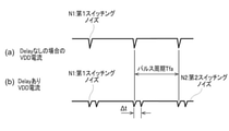
- FIG. 3 is a diagram showing an example of a power supply voltage VDD current flowing between the power supply voltage VDD and ground (GND).
- A The figure is a diagram showing an example of a power supply voltage VDD current when the delay processing by the delay circuit 404 is not performed.
- B The figure is a diagram showing an example of a power supply voltage VDD current when delay processing is performed by the delay circuit 404.
- the second switching noise N2 of the pulse period Tfa is added to the power supply voltage VDD current.
- FIG. 4 is a diagram schematically showing noise during electroacoustic conversion due to the power supply voltage VDD current.
- the vertical axis shows the power of noise, and the horizontal axis shows the frequency.
- A The figure is a case where the delay processing by the delay circuit 404 is not performed.
- B The figure is the case where the delay processing by the delay circuit 404 is performed.
- the noise component of the frequency f 1 / (2 ⁇ ⁇ t) is reduced.
- FIG. 5 is a diagram illustrating reduction of high frequency noise.
- A The figure shows impulse-like noise.
- the vertical axis shows the intensity of noise, and the horizontal axis shows time.
- B is a diagram showing the impulse-like noise in (a) by frequency.
- the vertical axis shows power and the horizontal axis shows frequency.
- the figure (c) shows an impulse-like noise with an interval ⁇ t.
- the vertical axis shows the intensity of noise, and the horizontal axis shows time.
- the figure (d) is a figure which showed the impulse-like noise of the figure (c) by frequency.
- the vertical axis shows power and the horizontal axis shows frequency.
- the magnitude of the impulse-like noise in (c) is 0.5 of the impulse-like noise in (a)
- the total energy of the noise power shown in (d) is (b). It is 0.5 squared x 2 of the total energy of the noise power shown by. That is, the total energy of the noise power shown in the figure (d) is 1/2 of the total energy of the noise power shown in the figure (b).
- FIG. 6 is a diagram illustrating the reduction of the noise component in FIG. (A)
- the figure shows an impulse-like noise having a period T (1 / fc).
- the vertical axis shows the intensity of noise, and the horizontal axis shows time.
- (B) is a diagram showing the impulse-like noise in (a) by frequency.
- the vertical axis shows power and the horizontal axis shows frequency.
- the figure (c) shows the impulse-like noise of the communication frequency fc and the impulse-like noise delayed by ⁇ t.
- the vertical axis shows power and the horizontal axis shows frequency.
- the figure (d) is a figure which showed the impulse-like noise of the figure (c) by frequency.
- the vertical axis shows power and the horizontal axis shows frequency.
- the second switching noise N2 caused by the second pulse signal is also delayed by ⁇ t.
- the magnitude of the noise pulse is halved.
- the total energy of the first switching noise N1 shown in FIG. 6B is 1
- the total energy of the noise power shown in FIG. 6D is twice the square of 0.5. .. That is, the total energy of the noise power shown in the figure (d) is 1/2 of the total energy of the noise power shown in the figure (b).
- communication applied to the power supply voltage VDD current by relatively delaying one of the first pulse signal and the second pulse signal by the delay circuit 404.
- the electroacoustic noise caused by the pulse-like noise of the frequency fc is suppressed.
- the electroacoustic noise caused by being applied to the power supply voltage VDD current is suppressed more efficiently. As a result, it is possible to suppress deterioration of the sound quality of the headphones 500, which is affected by the noise applied to the source voltage VDD current.
- the first pulse signal generated by the pulse generator 416 is delayed by a D flip-flop connected in sequence to generate a second pulse signal. It is different from the electroacoustic conversion device 1 according to the first embodiment.
- the differences from the electroacoustic conversion device 1 according to the first embodiment will be described.
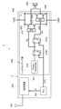
- FIG. 7A is a diagram showing an example of the configuration of the electroacoustic conversion device 1 according to the second embodiment. As shown in FIG. 7, a frequency signal having a communication frequency of 2 ⁇ fc is supplied to the D flip-flops 414b and c.
- a first pulse signal is input to the D terminal of the D flip-flop 414b, and a clock signal having a frequency of 2 ⁇ fc is supplied to the CL terminal.
- the D flip-flop 414c is connected longitudinally to the D flip-flop 414b. That is, the Q terminal of the D flip-flop 414b and the D terminal of the D flip-flop 414c are connected, and a clock signal having a frequency of 2 ⁇ fc is supplied to the CL terminal of the D flip-flop 414c.
- the first D flip-flop 414b reads the D signal at the rising edge of the CLK signal.
- the obtained first pulse signal Sp is taken in by the second D flip-flop 414c at the rising edge of the CLK signal.
- the obtained 2 pulse signal Sn is generated as a signal delayed by 1 clock from the first pulse signal Sp.
- the second pulse signal Sn delayed by one clock is output with respect to the first pulse signal Sp. That is, the second pulse signal Sn delayed by one cycle of the frequency (2 ⁇ fc) with respect to the first pulse signal Sp is output from the Q terminal of the flip-flop 414c.
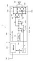
- FIG. 7B is a diagram showing another example of the configuration of the electroacoustic conversion device 1 according to the second embodiment.
- a frequency signal having a communication frequency fc is supplied to the D flip-flop 414b.
- the delay element 414d supplies a frequency signal delayed by half a cycle of the communication frequency fc to the lip flop 414c.
- the second pulse signal Sn delayed by one clock is output with respect to the first pulse signal Sp. That is, the second pulse signal Sn delayed by one cycle of the frequency (2 ⁇ fc) with respect to the first pulse signal Sp is output from the Q terminal of the flip-flop 414c.
- one of the first pulse signal and the second pulse signal is relatively divided into cycles based on the communication frequency fc by the connected D flip-flops 414b and 414c. I decided to delay it. As a result, the electroacoustic noise caused by the impulse-like noise of the communication frequency fc applied to the power supply voltage VDD current is suppressed.
- the electroacoustic conversion device 1 according to the modified example of the second embodiment is different from the electroacoustic conversion device 1 according to the second embodiment in that the operating time of the D flip-flops 414b and 414c is shortened.
- the differences from the electroacoustic conversion device 1 according to the second embodiment will be described.
- FIG. 8A is a diagram showing an example of the configuration of the electroacoustic conversion device 1 according to the modified example of the second embodiment. As shown in FIG. 8A, the delay circuit 414d, e, the exclusive OR circuit 414f, and the ethical product circuit 414g are further included.
- FIG. 8B is a diagram showing another example of the configuration of the electroacoustic conversion device 1 according to the modified example of the second embodiment. As shown in FIG. 8B, the delay circuit 414d, e, the exclusive OR circuit 414f, and the ethical product circuit 414g may be further provided with respect to the configuration of the electroacoustic conversion device 1 shown in FIG. 7B.
- One end of the delay circuit 414d is connected to the output terminal of the pulse generator 416, and the other end is connected to the input terminal of the delay circuit 414e and the D terminal of the D flip-flop 414b.
- One end of the delay circuit 414e is connected to the output terminal of the delay circuit 414d, and the other end is connected to the input terminal of the exclusive OR circuit 414f.
- the output terminal of the delay circuit 414e and the output terminal of the pulse generator 402 are connected to each input terminal of the exclusive OR circuit 414f.
- the input terminal of the AND circuit 414g is connected to the output terminal.
- the output terminal of the exclusive OR circuit 414f and the output terminal of the pulse generator 416 are connected to each input terminal of the ethical product circuit 414g. On the other hand, the output terminal is connected to the CL terminal of the D flip-flops 414b and 414c.
- FIG. 9 is a diagram showing an example of the output signal St4 of the AND circuit 414g when the first pulse signal Spt1 is output to the pulse generator 402.
- the vertical axis shows the magnitude of the signal, and the horizontal axis shows the time t.
- the figure (a) shows the first pulse signal Spt1 generated by the pulse generator 402, and the figure (b) shows the delay circuit 414d that the first pulse signal Spt1 has a delay time Td and a delayed first pulse.
- the signal Spt2 is shown.
- the figure (c) further shows the delay time Td of the first pulse signal Spt2 and the delayed first pulse signal Spt3 by the delay circuit 414d.
- the figure shows the output signal of the AND circuit 414g. As shown in FIG. 8, the first pulse signal Spt1 is output as the first pulse signal Spt2 to the input terminal of the delay circuit 414d and the D terminal of the D flip-flop 414b after the delay time Td.
- the delay circuit 414d outputs the third pulse signal Spt3 to the input terminal of the AND circuit 414g after the delay time Td.
- the exclusive OR circuit 414f outputs the other OR of the first pulse signal Spt1 and the third pulse signal Spt3 as the output signal St4. That is, the exclusive-OR circuit 414f uses the rising edge and the falling edge of the first pulse signal Spt2, which is an input signal to the D terminal of the D flip-flop 414b, as a reference time point, and sets the period Td before and after the period Td as a high level signal.
- the output signal St4 is output.
- the ethical product circuit 414g sends a clock signal to the CL terminal of the D flip-flops 414b and 414c whose high level is the period in which the high level period of the output signal St4 and the high level period of the clock signal of the frequency fc2 / 2 are superimposed. Supply.
- the pulse generator 402 outputs a Td clock signal from the rising and falling edges of the first pulse signal Spt2 for a certain period of time. It is supplied to the CL terminal of the flip-flops 414b and 414c.
- the operation of the D flip-flops 414b and 414c is limited to Td for a certain period of time from the rising and falling edges of the first pulse signal Spt2, and the power consumption of the D flip-flops 414b and 414c can be further reduced. ..
- a voltage based on a DC power supply is applied to one end of the electroacoustic converter in response to the first pulse signal, and a voltage based on the DC power supply is applied to the other end of the electroacoustic converter in response to the second pulse signal.
- the switching element part to apply A delay circuit that causes a delay based on the communication frequency with respect to at least one of the first pulse signal and the second pulse signal. Equipped with electronic devices.
- the switching element unit is The first and second switching elements connected in series to the DC power supply, It has a third and fourth switching element connected in series to the DC power supply, and has. Claim 1 that one end of the electroacoustic converter is connected to the connection point of the first and second switching elements, and the other end is connected to the connection point of the third and fourth switching elements.
- the electronic device according to any one of 3 to 3.
- the first switching element is turned on and off by the first pulse signal
- the second switching element is turned off when the first switching element is turned on
- the first switching element is turned off.
- the first gate control circuit that turns on when The third switching element is turned on and off by the second pulse signal
- the fourth switching element is turned off when the third switching element is turned on
- the third switching element is turned on when the third switching element is turned off.
- the first pulse signal and the pulse generator for generating the second pulse signal are further provided, and the first pulse signal is a pulse signal having a duty ratio according to the level of the voice signal.
- the electronic device according to any one of claims 1 to 5, wherein the second pulse signal is a pulse signal having a duty ratio according to the level of the voice signal.
- the delay circuit causes a delay of the first delay time based on the cycle of the communication frequency, the first pulse signal, and a delay of the second delay time based on the cycle of the communication frequency.
- the delay circuit is A first flip-flop circuit in which the pulse signal is input to the D terminal, a clock signal based on the cycle of the communication frequency is input to the clock terminal, and the first pulse signal is output from the Q terminal.
- a second flip-flop circuit in which the first pulse signal is input to the D terminal, the clock signal is input to the clock terminal, and the second pulse signal is output from the Q terminal.
- the delay circuit is The first delay circuit to which the pulse signal is input and The second delay circuit to which the output signal of the first delay circuit is input and The pulse signal, the exclusive OR circuit to which the output signal of the second delay circuit is input, and An ethical AND circuit in which the output signal of the exclusive OR circuit and the clock signal based on the cycle of the communication frequency are input, and A first flip-flop circuit in which the output signal of the first delay circuit is input to the D terminal, the output signal of the ethical product circuit is input to the clock terminal, and the first pulse signal is output from the Q terminal. A second flipflop circuit in which the first pulse signal is input to the D terminal, the output signal of the ethical product circuit is input to the clock terminal, and the second pulse signal is output from the Q terminal.
- Item 7. The electronic device according to Item 7.
- the electronic device according to claim 10 or 11, further comprising a communication device that performs at least one of transmission and reception at the communication frequency based on the reference frequency.
- a communication device that performs at least one of transmission and reception at the communication frequency, and It is equipped with a switching element unit that applies a voltage based on a DC power supply to an electroacoustic converter in response to two pulse signals based on an audio signal.
- An electronic device in which at least one of the two pulse signals is delayed in a cycle based on the communication frequency.
- An electroacoustic converter comprising the electronic device according to any one of claims 1 to 13 and the electroacoustic converter.
- Electro-acoustic converter 1: Electro-acoustic converter
- 2 Electronic equipment
- 200 Communication device
- 300 Frequency synthesizer
- 402 Pulse generator
- 404 Delay circuit
- 405 Switching element unit
- 406 First gate control circuit
- 408, 410 1st switching element
- 412 2nd gate control circuit
- 414, 416 2nd switching element
- 414b D flip-flop
- 414c D flip-flop
- 414d delay circuit
- 414e delay circuit
- 414f exclusive logic Japanese circuit
- 414g Ethical product circuit
- 500 Headphones.
Landscapes
- Engineering & Computer Science (AREA)
- Signal Processing (AREA)
- Computer Networks & Wireless Communication (AREA)
- Power Engineering (AREA)
- Multimedia (AREA)
- Physics & Mathematics (AREA)
- Acoustics & Sound (AREA)
- Circuit For Audible Band Transducer (AREA)
- Amplifiers (AREA)
Abstract
[課題]ノイズを抑制可能な電子機器、および電気音響変換装置を提供する。 [解決手段]本開示では、第1のパルス信号に応じて電気音響変換器の一端に直流電源に基づく電圧を印加し、第2のパルス信号に応じて電気音響変換器の他端に直流電源に基づく電圧を印加するスイッチング素子部と、第1のパルス信号、及び第2のパルス信号の少なくとも一方に対して、通信周波数に基づく遅延を生じさせる遅延回路と、を備える、電子機器が提供される。
Description
本開示は、電子機器、および電気音響変換装置に関する。
微弱なオーディオ信号を増幅し、スピーカやヘッドホンなどの電気音響変換素子を駆するために、電子機器が用いられる。また、スマートフォンなどの端末は、音声信号に基づく音声を聞きながら、無線通信なども行われる。ところが、電気音響変換により発生するノイズが送受信信号の通信周波数を妨害する恐れがある。
本開示の一態様は、ノイズを抑制可能な電子機器、および電気音響変換装置を提供する。
上記の課題を解決するために、本開示では、第1のパルス信号に応じて電気音響変換器の一端に直流電源に基づく電圧を印加し、第2のパルス信号に応じて前記電気音響変換器の他端に前記直流電源に基づく電圧を印加するスイッチング素子部と、
第1のパルス信号、及び前記第2のパルス信号の少なくとも一方に対して、通信周波数に基づく遅延を生じさせる遅延回路と、
を備える、電子機器が提供される。
第1のパルス信号、及び前記第2のパルス信号の少なくとも一方に対して、通信周波数に基づく遅延を生じさせる遅延回路と、
を備える、電子機器が提供される。
前記遅延回路は、前記通信周波数の周期に基づく遅延時間を生じさせてもよい。
前記遅延時間は、前記通信周波数の周期の2分の1であってもよい。
前記スイッチング素子部は、
前記直流電源に直列接続された第1,第2のスイッチング素子と、
前記直流電源に直列接続された第3,第4のスイッチング素子と、を有し、
前記電気音響変換器の一端は、前記第1,第2のスイッチング素子の接続点に接続され、他端は、と前記第3,第4のスイッチング素子の接続点に接続されてもよい。
前記直流電源に直列接続された第1,第2のスイッチング素子と、
前記直流電源に直列接続された第3,第4のスイッチング素子と、を有し、
前記電気音響変換器の一端は、前記第1,第2のスイッチング素子の接続点に接続され、他端は、と前記第3,第4のスイッチング素子の接続点に接続されてもよい。
前記第1のスイッチング素子を前記第1のパルス信号でオン、オフし、前記第2のスイッチング素子を前記第1 のスイッチング素子がオンするときオフし、前記第1 のスイッチング素子がオフするときオンする第1ゲート制御回路と、
前記第3のスイッチング素子を前記第2のパルス信号でオン、オフし、前記第4のスイッチング素子を前記第3 のスイッチング素子がオンするときオフし、前記第3のスイッチング素子がオフするときオンする第3ゲート制御回路と、を
更に備えてもよい。
前記第3のスイッチング素子を前記第2のパルス信号でオン、オフし、前記第4のスイッチング素子を前記第3 のスイッチング素子がオンするときオフし、前記第3のスイッチング素子がオフするときオンする第3ゲート制御回路と、を
更に備えてもよい。
前記第1のパルス信号と、前記第2のパルス信号を生成するパルス生成器を更に備え、前記第1のパルス信号は、音声信号のレベルに応じたデューティ比を有するパルス信号であり、前記第2のパルス信号は、前記音声信号のレベルに応じたデューティ比を有するパルス信号であってもよい。
音声信号のレベルに応じたパルス信号を生成するパルス生成器を更に備え、
前記前記遅延回路は、前記通信周波数の周期に基づく第1遅延時間の遅延を生じさせた前記第1のパルス信号と、前記通信周波数の周期に基づく第2遅延時間の遅延を生じさせた前記第2のパルス信号とを生成してもよい。
前記前記遅延回路は、前記通信周波数の周期に基づく第1遅延時間の遅延を生じさせた前記第1のパルス信号と、前記通信周波数の周期に基づく第2遅延時間の遅延を生じさせた前記第2のパルス信号とを生成してもよい。
前記遅延回路は、
D端子に前記パルス信号が入力され、クロック端子に前記通信周波数の周期に基づくクロック信号が入力され、Q端子から前記第1のパルス信号が出力される第1フリップフロップ回路と、
D端子に前記第1のパルス信号が入力され、クロック端子に前記クロック信号が入力され、Q端子から前記第2のパルス信号が出力される第2フリップフロップ回路と、
を有してもよい。
D端子に前記パルス信号が入力され、クロック端子に前記通信周波数の周期に基づくクロック信号が入力され、Q端子から前記第1のパルス信号が出力される第1フリップフロップ回路と、
D端子に前記第1のパルス信号が入力され、クロック端子に前記クロック信号が入力され、Q端子から前記第2のパルス信号が出力される第2フリップフロップ回路と、
を有してもよい。
前記遅延回路は、
前記パルス信号が入力される第1遅延回路と、
前記第1遅延回路の出力信号が入力される第2遅延回路と、
前記パルス信号と、第2遅延回路の出力信号が入力される排他的論理和回路と、
前記排他的論理和回路の出力信号と、前記通信周波数の周期に基づくクロック信号とが入力される倫理積回路と、
D端子に前記第1遅延回路の出力信号が入力され、クロック端子に前記倫理積回路の出力信号が入力され、Q端子から前記第1のパルス信号が出力される第1フリップフロップ回路と、
D端子に前記第1のパルス信号が入力されクロック端子に前記倫理積回路の出力信号が入力され、Q端子から前記第2のパルス信号が出力される第2フリップフロップ回路と、を有してもよい。
前記パルス信号が入力される第1遅延回路と、
前記第1遅延回路の出力信号が入力される第2遅延回路と、
前記パルス信号と、第2遅延回路の出力信号が入力される排他的論理和回路と、
前記排他的論理和回路の出力信号と、前記通信周波数の周期に基づくクロック信号とが入力される倫理積回路と、
D端子に前記第1遅延回路の出力信号が入力され、クロック端子に前記倫理積回路の出力信号が入力され、Q端子から前記第1のパルス信号が出力される第1フリップフロップ回路と、
D端子に前記第1のパルス信号が入力されクロック端子に前記倫理積回路の出力信号が入力され、Q端子から前記第2のパルス信号が出力される第2フリップフロップ回路と、を有してもよい。
前記遅延回路は、
前記パルス信号が入力される第1遅延回路と、
前記第1遅延回路の出力信号が入力される第2遅延回路と、
前記パルス信号と、第2遅延回路の出力信号が入力される排他的論理和回路と、
前記排他的論理和回路の出力信号と、前記通信周波数の周期に基づくクロック信号とが入力される倫理積回路と、
D端子に前記第1遅延回路の出力信号が入力され、クロック端子に前記倫理積回路の出力信号が入力され、Q端子から前記第1のパルス信号が出力される第1フリップフロップ回路と、
D端子に前記第1のパルス信号が入力されクロック端子に前記倫理積回路の出力信号が入力され、Q端子から前記第2のパルス信号が出力される第2フリップフロップ回路と、を有してもよい。
前記パルス信号が入力される第1遅延回路と、
前記第1遅延回路の出力信号が入力される第2遅延回路と、
前記パルス信号と、第2遅延回路の出力信号が入力される排他的論理和回路と、
前記排他的論理和回路の出力信号と、前記通信周波数の周期に基づくクロック信号とが入力される倫理積回路と、
D端子に前記第1遅延回路の出力信号が入力され、クロック端子に前記倫理積回路の出力信号が入力され、Q端子から前記第1のパルス信号が出力される第1フリップフロップ回路と、
D端子に前記第1のパルス信号が入力されクロック端子に前記倫理積回路の出力信号が入力され、Q端子から前記第2のパルス信号が出力される第2フリップフロップ回路と、を有してもよい。
前記通信周波数に応じて基準周波数の信号を生成する、周波数シンセサイザを更に備え、
前記遅延回路は、前記基準周波数の信号に基づき駆動してもよい。
前記遅延回路は、前記基準周波数の信号に基づき駆動してもよい。
前記周波数シンセサイザが出力する基準周波数は、時間帯に応じて切り換えてもよい。
前記基準周波数に基づく前記通信周波数により送信、及び受信の少なくとも一方を行う通信機を更に備えてもよい。
上記の課題を解決するために、本開示では、 前記通信周波数で送信、及び受信の少なくとも一方を行う通信機と、
音声信号に基づく2つのパルス信号に応じて電気音響変換器に直流電源に基づく電圧を印加するスイッチング素子部と、を備え、
前記2つのパルス信号の少なくとも一方は、前記通信周波数に基づく周期で遅延している、電子機器が提供される。
音声信号に基づく2つのパルス信号に応じて電気音響変換器に直流電源に基づく電圧を印加するスイッチング素子部と、を備え、
前記2つのパルス信号の少なくとも一方は、前記通信周波数に基づく周期で遅延している、電子機器が提供される。
上記の電子機器と、前記電気音響変換器とを備える、電気音響変換装置を提供してもよい。
以下、図面を参照して、電子機器、および電気音響変換装置の実施形態について説明する。以下では、電子機器、および電気音響変換装置の主要な構成部品分を中心に説明するが、電子機器、および電気音響変換装置には、図示又は説明されていない構成部品分や機能が存在しうる。以下の説明は、図示又は説明されていない構成部品分や機能を除外するものではない。
(第1実施形態)
図1を参照して、本実施形態に係る電子機器の構成について説明する。図1は、本実施形態に係る電気音響変換装置1の構成の一例を示す図である。電気音響変換装置1は、無線通信が可能であると共に音声信号Smの音響変換が可能な機器である。この電気音響変換装置1は、電子機器2と、アンテナ100と、ヘッドホン500とを備える。電子機器2は、通信機200と、周波数シンセサイザ300と、ヘッドホンアンプ部400とを有する。
図1を参照して、本実施形態に係る電子機器の構成について説明する。図1は、本実施形態に係る電気音響変換装置1の構成の一例を示す図である。電気音響変換装置1は、無線通信が可能であると共に音声信号Smの音響変換が可能な機器である。この電気音響変換装置1は、電子機器2と、アンテナ100と、ヘッドホン500とを備える。電子機器2は、通信機200と、周波数シンセサイザ300と、ヘッドホンアンプ部400とを有する。
アンテナ100は、無線周波数の受信信号を受信し、無線周波数の送信信号を送信する。
通信機200は、例えばBT受信機であり、アンテナ100で受信した、例えば2.4Ghz帯である通信周波数fcに対応する信号を増幅した後に、デジタル信号に変換する。BT受信機は、Bluetooth(登録商標)の省電力用途に特化したBLEに対応可能である。なお、本実施形態に係る通信機200は、例えばBT受信機であるが、これに限定されない。例えば、通信機200は、GNSS送受信機でもよい。
通信機200は、例えばBT受信機であり、アンテナ100で受信した、例えば2.4Ghz帯である通信周波数fcに対応する信号を増幅した後に、デジタル信号に変換する。BT受信機は、Bluetooth(登録商標)の省電力用途に特化したBLEに対応可能である。なお、本実施形態に係る通信機200は、例えばBT受信機であるが、これに限定されない。例えば、通信機200は、GNSS送受信機でもよい。
周波数シンセサイザ300は、通信機200の発振周波数fcをループ制御するフェーズドロックループ(PLL)回路である。周波数シンセサイザ300は、通信周波数fcの例えば2倍に対応する周波数2×fcの基準周波数信号を生成し、周波数fcの周波数信号を通信機200に供給する。
周波数シンセサイザ300は、例えば送受信信号の周波数帯域信号に基づき、基準周波数信号を生成する。例えば、周波数帯域信号は、Bluetoothに準拠している。例えば、2.402~2.480[GHz]の周波数が79分割される。つまり、2.402[GHz]、2.403[GHz]、2.404[GHz]、・・・、2.480[GHz]のいずれかの周波数を用いて通信が行われる。通信機200は、周波数シンセサイザ300が使用する周波数帯域を時間毎に切り替え(ホッピング)る。
ヘッドホンアンプ部400は、例えばフィルタレスD級アンプである。ヘッドホンアンプ部400は、パルス生成器402と、遅延回路404と、スイッチグ素子部405と、を備える。スイッチグ素子部405は、第1ゲート制御回路406と、第1スイッチグ素子408、410と、第2ゲート制御回路412と、第2スイッチグ素子414、416と、を有する。
このフィルタレスD級アンプは、フルブリッジ接続されたスイッチング素子408、410、414,416を、入力オーディオ信号Smの信号レベルに応じてパルス幅変調された所定周波数のパルス信号(PWM信号)でオン、オフスイッチングする。これにより、フルブリッジ接続されたフルブリッジ回路に負荷として接続されているヘッドホン500(電気音響変換器)を駆動する。
パルス生成器402は、音声信号Smに応じて、第1のパルス信(Sp信号)と、第2のパルス信号(Sn信号)とを生成する。例えば、第1のパルス信号は、音声信号Smのレベルに応じたデューティ比を有するパルス信号であり、第2のパルス信号は、音声信号Smのレベルに応じたデューティ比を有するパルス信号である、第1のパルス信号と、第2のパルス信号との生成方法には、様々な方法があり、既知の方法を用いることが可能である。
遅延回路404は、通信周波数fcに基づき、第1のパルス信号と、第2のパルス信号との一方を相対的にΔt遅延させる。例えば、遅延回路404は、第1のパルス信号に対して、第2のパルス信号を通信周波数fcの1/2周期(Δt=1/2fc)分遅延させる。本実施形態に係る遅延回路404は、第2のパルス信号を遅延させるがこれに限定されない。例えば、第1のパルス信号を遅延させてもよい。遅延回路404の詳細は、後述する。
上述のように、通信周波数fcに基づく信号は、周波数シンセサイザ300から供給される。このため、例えば、周波数シンセサイザ300が使用する周波数帯域を時間毎に切り替える(ホッピング)場合にも、通信周波数fcに基づく遅延を第2のパルス信号に生じさせることが可能である。
図2は、パルス生成器402が生成する第1のパルス信と、第2のパルス信号と、スピーカ印可電圧の関係を示す図である。ここでは、遅延がない場合の信号例を示す。(a)図は、第1のパルス信号を示し、(b)図は、第2のパルス信号を示し、(c)図は、スピーカ印可電圧を示す。横軸は時間である。図2は、例えば入力信号が正極性で中レベル時の状態を示す。
図2に示すように、パルス生成器402が生成する第1のパルス信号のデューティ比は50%より大きくなり、第2のパルス信号のデューティ比は50%より小さくなる。したがって、ヘッドホン500には(c)に示すように、例えば入力信号の正極性レベルに応じた正極性のパルス電圧が印加される。
再び図1に示すように、スイッチグ素子部405は、第1のパルス信号に応じてヘッドホン500の一端に直流電源VDDに基づく電圧を印加し、第2のパルス信号に応じてヘッドホン500の他端に直流電源VDDに基づく電圧を印加する。すなわち、直流電源VDDとグランドGNDとの間には、第1スイッチグ素子408、410による直列接続回路と、第2スイッチグ素子414、416による直列接続回路とがそれぞれ接続されている。第1スイッチグ素子408、410の中間点と第2スイッチグ素子414、416の中間点にヘッドホン500が接続される。このように、第1スイッチグ素子408、410と第2スイッチグ素子414、416によりフルブリッジ回路が構成され、第1スイッチグ素子408、410の中間点と第2スイッチグ素子414、416の中間点にヘッドホン500が接続される。
第1ゲート制御回路406は、第1のパルス信に応じて、第1スイッチグ素子408、410を互いに逆方向にオン、オフする。すなわち、第1スイッチグ素子408がオンのとき、第1スイッチグ素子410はオフに駆動され、第1スイッチグ素子408がオフのとき、第1スイッチグ素子410はオンに駆動される。
第2ゲート制御回路412は、第2のパルス信に応じて、第2スイッチグ素子414、416を互いに逆方向にオン、オフする。すなわち、第2スイッチグ素子414がオンのとき、第2スイッチグ素子416はオフに駆動され、第2スイッチグ素子414がオフのとき、第2スイッチグ素子416はオンに駆動される。
ここで、図3に基づき、遅延回路404の制御例の詳細を説明する。
図3は、電源電圧VDDとグランド(GND)間に流れる電源電圧VDD電流の例を示す図である。(a)図は、遅延回路404による遅延処理を行わない場合の電源電圧VDD電流の例を示す図である。(b)図は、遅延回路404による遅延処理を行った場合の電源電圧VDD電流の例を示す図である。
図3は、電源電圧VDDとグランド(GND)間に流れる電源電圧VDD電流の例を示す図である。(a)図は、遅延回路404による遅延処理を行わない場合の電源電圧VDD電流の例を示す図である。(b)図は、遅延回路404による遅延処理を行った場合の電源電圧VDD電流の例を示す図である。
(a)図に示すように、遅延回路404による遅延処理を行わない場合には、電源電圧VDD電流には、ヘッドホンアンプ部400におけるパルス周期Tfaの第1スイッチングノイズN1が発生する。これにより、ヘッドホン500では、電気音響変換の際に第1スイッチングノイズN1に起因するノイズが発生する。なお、本実施形態では、電気音響変換の際に生じるノイズを気音響変換ノイズと称することとする。
一方で、遅延回路404によるΔt=1/2fcの遅延処理を第2のパルス信号に行った場合には、パルス周期Tfaの第1スイッチングノイズN1の他に、第1スイッチングノイズN1からΔt遅延するパルス周期Tfaの第2スイッチングノイズN2が電源電圧VDD電流に追加される。
図4は、電源電圧VDD電流に起因する電気音響変換の際のノイズを模式的に示す図である。縦軸はノイズのパワーを示し、横軸は周波数を示す。(a)図は、遅延回路404による遅延処理を行わない場合である。(b)図は、遅延回路404による遅延処理を行った場合である。(b)図に示すように、周波数f=1/(2×Δt)のノイズ成分が低減される。
図5は、高域ノイズの低減を説明する図である。(a)図は、インパルス状のノイズを示す。縦軸はノイズの強度、横軸は時間を示す。(b)図は、(a)図のインパルス状のノイズを周波数で示した図である。縦軸はパワー、横軸は周波数を示す。
(c)図は、間隔Δtのインパルス状のノイズを示す。縦軸はノイズの強度、横軸は時間を示す。(d)図は、(c)図のインパルス状のノイズを周波数で示した図である。縦軸はパワー、横軸は周波数を示す。(d)図で示すように、(b)図と比較すると、周波数f=1/(2×Δt)のノイズ成分が低減される。この場合、(c)図のインパルス状のノイズの大きさが、(a)図のインパルス状のノイズの0.5とすると、(d)図で示すノイズパワーの総エネルギーは、(b)図で示すノイズパワーの総エネルギーの0.5の二乗×2となる。つまり、(d)図で示すノイズパワーの総エネルギーは、(b)図で示すノイズパワーの総エネルギーの1/2倍になる。
図6は、図4におけるノイズ成分の減少を説明する図である。(a)図は、周期T(1/fc)のインパルス状のノイズを示す。縦軸はノイズの強度、横軸は時間を示す。(b)図は、(a)図のインパルス状のノイズを周波数で示した図である。縦軸はパワー、横軸は周波数を示す。
(c)図は、通信周波数fcのインパルス状のノイズとΔt遅れたインパルス状のノイズを示す。縦軸はパワー、横軸は周波数を示す。(d)図は、(c)図のインパルス状のノイズを周波数で示した図である。縦軸はパワー、横軸は周波数を示す。(d)図で示すように、周波数f=1/(2×Δt)のノイズ成分が低減される。
図3に示すように、第1のパルス信号が第1ゲート制御回路406に、第2のパルス信号が第2ゲート制御回路412に、遅延無く加えられると、第1のパルス信号に起因するスイッチングノイズと、第2のパルス信号に起因するスイッチングノイズとが同時に生じ、第1スイッチングノイズN1となる。
一方で、例えば第2のパルス信号をΔt遅延させると、第2のパルス信号に起因する第2スイッチングノイズN2もΔt遅延する。この場合、スイッチングノイズの発生がずれるので、ノイズパルスの大きさは、半減する。再び図6を参照して、(b)図で示す第1スイッチングノイズN1の総エネルギーを1とすると、(d)図で示すノイズパワーの総エネルギーは、0.5の二乗の2倍となる。つまり、(d)図で示すノイズパワーの総エネルギーは、(b)図で示すノイズパワーの総エネルギーの1/2倍になる。
これらから分かるように、fc=1/(2×Δt)となるように遅延回路404によるΔtを設定すると、通信機200における通信周波数fcのインパルス状のノイズにより生じる電気音響変換ノイズのパワーを半減できる。このように、遅延回路404により、第1のパルス信号に対して第2のパルス信号に、Δt=2×fcの相対的な遅延を生じさせると、電源電圧VDD電流に印可される通信周波数fcの電流ノイズに起因する電気音響変換の際に生じるノイズが抑制される。
以上、説明したように、本実施形態によれば、遅延回路404により第1のパルス信号と、第2のパルス信号の一方を相対的に遅延させることにより、電源電圧VDD電流に印可される通信周波数fcのインパルス状のノイズに起因する電気音響ノイズが抑制される。特に、周期Δtを1/(2×fc)として遅延させることにより、より効率的に電源電圧VDD電流に印可される起因する電気音響イズが抑制される。これにより、源電圧VDD電流に印可されるノイズの影響を受けるヘッドホン500の音質の低下が抑制可能となる。
(第2実施形態)
第2実施形態に係る電気音響変換装置1は、パルス生成器416が生成する第1のパルス信号を縦続に接続させたDフリップフロップにより遅延させて、第2のパルス信号を生成される点で第1実施形態に係る電気音響変換装置1と相違する。以下では第1実施形態に係る電気音響変換装置1と相違する点を説明する。
第2実施形態に係る電気音響変換装置1は、パルス生成器416が生成する第1のパルス信号を縦続に接続させたDフリップフロップにより遅延させて、第2のパルス信号を生成される点で第1実施形態に係る電気音響変換装置1と相違する。以下では第1実施形態に係る電気音響変換装置1と相違する点を説明する。
図7Aは、第2実施形態に係る電気音響変換装置1の構成の一例を示す図である。図7に示すように、通信周波数2×fcの周波数信号がDフリップフロップ414b、cに供給する。
Dフリップフロップ414bのD端子には、第1のパルス信号が入力され、CL端子には周波数2×fcのクロック信号が供給される。Dフリップフロップ414cは、Dフリップフロップ414bに縦続に接続さる。すなわち、Dフリップフロップ414bのQ端子とDフリップフロップ414cのD端子とが接続され、Dフリップフロップ414cのCL端子には周波数2×fcのクロック信号が供給される。
このような、縦続に接続させたDフリップフロップでは、Dフリップフロップ414bのD端子に第1のパルス信号を加えると、一つ目のDフリップフロップ414bがD信号をCLK信号の立ち上がりで読み取り、得られた第1のパルス信号Spを2つ目のDフリップフロップ414cがCLK信号の立ち上がりで取り込む。これにより、得られる2のパルス信号Snは、第1のパルス信号Spより1クロック遅れた信号として生成される。このように、第1のパルス信号Spに対して、1クロック遅延した第2のパルス信号Snが出力される。すなわち、第1のパルス信号Spに対して、周波数(2×fc)の1周期分遅延した第2のパルス信号Snがフリップフロップ414cのQ端子から出力される。
図7Bは、第2実施形態に係る電気音響変換装置1の構成の別の一例を示す図である。図7Bに示すように、通信周波数fcの周波数信号がDフリップフロップ414bに供給される。一方で遅延素子414dにより通信周波数fcの半周期分遅延した周波数信号がリップフロップ414cに供給される。これにより、第1のパルス信号Spに対して、1クロック遅延した第2のパルス信号Snが出力される。すなわち、第1のパルス信号Spに対して、周波数(2×fc)の1周期分遅延した第2のパルス信号Snがフリップフロップ414cのQ端子から出力される。
以上、説明したように、本実施形態によれば、接続させたDフリップフロップ414b、414cにより第1のパルス信号と、第2のパルス信号の一方を通信周波数fcに基づく周期分を相対的に遅延させることとした。これにより、電源電圧VDD電流に印可される通信周波数fcのインパルス状のノイズに起因する電気音響イズが抑制される。
(第2実施形態の変形例)
第2実施形態の変形例に係る電気音響変換装置1は、Dフリップフロップ414b、414cの動作時間を短縮させる点で第2実施形態に係る電気音響変換装置1と相違する。以下では第2実施形態に係る電気音響変換装置1と相違する点を説明する。
第2実施形態の変形例に係る電気音響変換装置1は、Dフリップフロップ414b、414cの動作時間を短縮させる点で第2実施形態に係る電気音響変換装置1と相違する。以下では第2実施形態に係る電気音響変換装置1と相違する点を説明する。
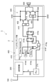
図8Aは、第2実施形態の変形例に係る電気音響変換装置1の構成の一例を示す図である。図8Aに示すように、遅延回路414d、eと、排他的論理和回路414fと、倫理積回路414gとを更に有する。
図8Bは、第2実施形態の変形例に係る電気音響変換装置1の構成の別の一例を示す図である。図8Bに示すように、図7Bで示した電気音響変換装置1の構成に対して遅延回路414d、eと、排他的論理和回路414fと、倫理積回路414gとを更に有してもよい。
遅延回路414dの一端は、パルス生成器416の出力端子に接続され、他端は、遅延回路414eの入力端子とDフリップフロップ414bのD端子とに接続される。遅延回路414eの一端は、遅延回路414dの出力端子に接続され、他端は、排他的論理和回路414fの入力端子に接続される。
排他的論理和回路414fのそれぞれの入力端子には、遅延回路414eの出力端子と、パルス生成器402の出力端子とが接続される。一方で、出力端子には、倫理積回路414gの入力端子が接続される。
倫理積回路414gのそれぞれの入力端子には、排他的論理和回路414fの出力端子と、パルス生成器416の出力端子とが接続さる。一方で、出力端子は、Dフリップフロップ414b、414cのCL端子に接続される。
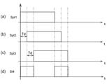
図9は、第1のパルス信号Spt1がパルス生成器402出力された際の倫理積回路414gの出力信号St4の例を示す図である。縦軸は信号の大きさを示し、横軸は時間tを示す。(a)図は、パルス生成器402の生成した第1のパルス信号Spt1を示し、(b)図は、遅延回路414dにより、第1のパルス信号Spt1が遅延時間Td、遅延した第1のパルス信号Spt2を示す。
(c)図は、更に遅延回路414dにより、第1のパルス信号Spt2が遅延時間Td、遅延した第1のパルス信号Spt3を示す。(d)図は、倫理積回路414gの出力信号を示す。図8に示すように、第1のパルス信号Spt1は、遅延時間Tdの後に、第1のパルス信号Spt2として、遅延回路414dの入力端子とDフリップフロップ414bのD端子とに出力される。
遅延回路414dは、遅延時間Tdの後に、第3のパルス信号Spt3を倫理積回路414gの入力端子に出力する。そして、排他的論理和回路414fは、第1のパルス信号Spt1と第3のパルス信号Spt3との他的論理和を出力信号St4として出力する。すなわち、排他的論理和回路414fは、Dフリップフロップ414bのD端子への入力信号である第1のパルス信号Spt2の立ち上がりと、立ち下がりを基準時点として、前後の期間Tdをハイレベル信号とする出力信号St4を出力する。
これにより、倫理積回路414gは、出力信号St4のハイレベル期間と周波数fc2/2のクロック信号のハイレベル期間が重畳する期間をハイレベルとするクロック信号をDフリップフロップ414b、414cのCL端子に供給する。
このように、第2実施形態の変形例に係る電気音響変換装置1は、パルス生成器402が出力に基づく、第1のパルス信号Spt2の立ち上がり及び立ち下がりエッジから一定時間Tdのクロック信号をDフリップフロップ414b、414cのCL端子に供給する。これにより、Dフリップフロップ414b、414cの動作が第1のパルス信号Spt2の立ち上がり及び立ち下がりエッジから一定時間Tdに限定され、Dフリップフロップ414b、414cの消費電力をより小さくすることが可能となる。
なお、本技術は以下のような構成を取ることができる。
(1)第1のパルス信号に応じて電気音響変換器の一端に直流電源に基づく電圧を印加し、第2のパルス信号に応じて前記電気音響変換器の他端に前記直流電源に基づく電圧を印加するスイッチング素子部と、
第1のパルス信号、及び前記第2のパルス信号の少なくとも一方に対して、通信周波数に基づく遅延を生じさせる遅延回路と、
を備える、電子機器。
第1のパルス信号、及び前記第2のパルス信号の少なくとも一方に対して、通信周波数に基づく遅延を生じさせる遅延回路と、
を備える、電子機器。
(2)前記遅延回路は、前記通信周波数の周期に基づく遅延時間を生じさせる、請求項1に記載の電子機器。
(3)前記遅延時間は、前記通信周波数の周期の2分の1である、請求項2に記載の電子機器。
(4)前記スイッチング素子部は、
前記直流電源に直列接続された第1,第2のスイッチング素子と、
前記直流電源に直列接続された第3,第4のスイッチング素子と、を有し、
前記電気音響変換器の一端は、前記第1,第2のスイッチング素子の接続点に接続され、他端は、と前記第3,第4のスイッチング素子の接続点に接続される、請求項1乃至3のいずれか一項に記載の電子機器。
前記直流電源に直列接続された第1,第2のスイッチング素子と、
前記直流電源に直列接続された第3,第4のスイッチング素子と、を有し、
前記電気音響変換器の一端は、前記第1,第2のスイッチング素子の接続点に接続され、他端は、と前記第3,第4のスイッチング素子の接続点に接続される、請求項1乃至3のいずれか一項に記載の電子機器。
(5)前記第1のスイッチング素子を前記第1のパルス信号でオン、オフし、前記第2のスイッチング素子を前記第1のスイッチング素子がオンするときオフし、前記第1のスイッチング素子がオフするときオンする第1ゲート制御回路と、
前記第3のスイッチング素子を前記第2のパルス信号でオン、オフし、前記第4のスイッチング素子を前記第3のスイッチング素子がオンするときオフし、前記第3のスイッチング素子がオフするときオンする第3ゲート制御回路と、を
更に備える、請求項4に記載の電子機器。
前記第3のスイッチング素子を前記第2のパルス信号でオン、オフし、前記第4のスイッチング素子を前記第3のスイッチング素子がオンするときオフし、前記第3のスイッチング素子がオフするときオンする第3ゲート制御回路と、を
更に備える、請求項4に記載の電子機器。
(6)前記第1のパルス信号と、前記第2のパルス信号を生成するパルス生成器を更に備え、前記第1のパルス信号は、音声信号のレベルに応じたデューティ比を有するパルス信号であり、前記第2のパルス信号は、前記音声信号のレベルに応じたデューティ比を有するパルス信号である、請求項1乃至5のいずれか一項に記載の電子機器。
(7)音声信号のレベルに応じたパルス信号を生成するパルス生成器を更に備え、
前記前記遅延回路は、前記通信周波数の周期に基づく第1遅延時間の遅延を生じさせた前記第1のパルス信号と、前記通信周波数の周期に基づく第2遅延時間の遅延を生じさせた前記第2のパルス信号とを生成する、請求項1乃至5のいずれか一項に記載の電子機器。
前記前記遅延回路は、前記通信周波数の周期に基づく第1遅延時間の遅延を生じさせた前記第1のパルス信号と、前記通信周波数の周期に基づく第2遅延時間の遅延を生じさせた前記第2のパルス信号とを生成する、請求項1乃至5のいずれか一項に記載の電子機器。
(8)前記遅延回路は、
D端子に前記パルス信号が入力され、クロック端子に前記通信周波数の周期に基づくクロック信号が入力され、Q端子から前記第1のパルス信号が出力される第1フリップフロップ回路と、
D端子に前記第1のパルス信号が入力され、クロック端子に前記クロック信号が入力され、Q端子から前記第2のパルス信号が出力される第2フリップフロップ回路と、
を有する、請求項7に記載の電子機器。
D端子に前記パルス信号が入力され、クロック端子に前記通信周波数の周期に基づくクロック信号が入力され、Q端子から前記第1のパルス信号が出力される第1フリップフロップ回路と、
D端子に前記第1のパルス信号が入力され、クロック端子に前記クロック信号が入力され、Q端子から前記第2のパルス信号が出力される第2フリップフロップ回路と、
を有する、請求項7に記載の電子機器。
(9)前記遅延回路は、
前記パルス信号が入力される第1遅延回路と、
前記第1遅延回路の出力信号が入力される第2遅延回路と、
前記パルス信号と、第2遅延回路の出力信号が入力される排他的論理和回路と、
前記排他的論理和回路の出力信号と、前記通信周波数の周期に基づくクロック信号とが入力される倫理積回路と、
D端子に前記第1遅延回路の出力信号が入力され、クロック端子に前記倫理積回路の出力信号が入力され、Q端子から前記第1のパルス信号が出力される第1フリップフロップ回路と、
D端子に前記第1のパルス信号が入力されクロック端子に前記倫理積回路の出力信号が入力され、Q端子から前記第2のパルス信号が出力される第2フリップフロップ回路と、を有する、請求項7に記載の電子機器。
前記パルス信号が入力される第1遅延回路と、
前記第1遅延回路の出力信号が入力される第2遅延回路と、
前記パルス信号と、第2遅延回路の出力信号が入力される排他的論理和回路と、
前記排他的論理和回路の出力信号と、前記通信周波数の周期に基づくクロック信号とが入力される倫理積回路と、
D端子に前記第1遅延回路の出力信号が入力され、クロック端子に前記倫理積回路の出力信号が入力され、Q端子から前記第1のパルス信号が出力される第1フリップフロップ回路と、
D端子に前記第1のパルス信号が入力されクロック端子に前記倫理積回路の出力信号が入力され、Q端子から前記第2のパルス信号が出力される第2フリップフロップ回路と、を有する、請求項7に記載の電子機器。
(10)前記通信周波数に応じて基準周波数の信号を生成する、周波数シンセサイザを更に備え、
前記遅延回路は、前記基準周波数の信号に基づき駆動する、請求項1乃至9のいずれか一項に記載の電子機器。
前記遅延回路は、前記基準周波数の信号に基づき駆動する、請求項1乃至9のいずれか一項に記載の電子機器。
(11)前記周波数シンセサイザが出力する基準周波数は、時間帯に応じて切り換えられる、請求項10に記載の電子機器。
(12)前記基準周波数に基づく前記通信周波数により送信、及び受信の少なくとも一方を行う通信機を更に備える、請求項10又は11に記載の電子機器。
(13)前記通信周波数で送信、及び受信の少なくとも一方を行う通信機と、
音声信号に基づく2つのパルス信号に応じて電気音響変換器に直流電源に基づく電圧を印加するスイッチング素子部と、を備え、
前記2つのパルス信号の少なくとも一方は、前記通信周波数に基づく周期で遅延している、電子機器。
音声信号に基づく2つのパルス信号に応じて電気音響変換器に直流電源に基づく電圧を印加するスイッチング素子部と、を備え、
前記2つのパルス信号の少なくとも一方は、前記通信周波数に基づく周期で遅延している、電子機器。
(14)請求項1乃至13のいずれか一項に記載の電子機器と、前記電気音響変換器とを備える、電気音響変換装置。
本開示の態様は、上述した個々の実施形態に限定されるものではなく、当業者が想到しうる種々の変形も含むものであり、本開示の効果も上述した内容に限定されない。すなわち、特許請求の範囲に規定された内容およびその均等物から導き出される本開示の概念的な思想と趣旨を逸脱しない範囲で種々の追加、変更および部分的削除が可能である。
1:電気音響変換装置、2:電子機器、200:通信機、300:周波数シンセサイザ、402:パルス生成器、404:遅延回路、405:スイッチグ素子部、406:第1ゲート制御回路、408、410:第1スイッチグ素子、412:第2ゲート制御回路、414、416:第2スイッチグ素子、414b:Dフリップフロップ、414c:Dフリップフロップ、414d:遅延回路、414e:遅延回路、414f:排他的論理和回路、414g:倫理積回路、500:ヘッドホン。
Claims (14)
- 第1のパルス信号に応じて電気音響変換器の一端に直流電源に基づく電圧を印加し、第2のパルス信号に応じて前記電気音響変換器の他端に前記直流電源に基づく電圧を印加するスイッチング素子部と、
第1のパルス信号、及び前記第2のパルス信号の少なくとも一方に対して、通信周波数に基づく遅延を生じさせる遅延回路と、
を備える、電子機器。 - 前記遅延回路は、前記通信周波数の周期に基づく遅延時間を生じさせる、請求項1に記載の電子機器。
- 前記遅延時間は、前記通信周波数の周期の2分の1である、請求項2に記載の電子機器。
- 前記スイッチング素子部は、
前記直流電源に直列接続された第1,第2のスイッチング素子と、
前記直流電源に直列接続された第3,第4のスイッチング素子と、を有し、
前記電気音響変換器の一端は、前記第1,第2のスイッチング素子の接続点に接続され、他端は、と前記第3,第4のスイッチング素子の接続点に接続される、請求項1に記載の電子機器。 - 前記第1のスイッチング素子を前記第1のパルス信号でオン、オフし、前記第2のスイッチング素子を前記第1のスイッチング素子がオンするときオフし、前記第1のスイッチング素子がオフするときオンする第1ゲート制御回路と、
前記第3のスイッチング素子を前記第2のパルス信号でオン、オフし、前記第4のスイッチング素子を前記第3のスイッチング素子がオンするときオフし、前記第3のスイッチング素子がオフするときオンする第3ゲート制御回路と、を
更に備える、請求項4に記載の電子機器。 - 前記第1のパルス信号と、前記第2のパルス信号を生成するパルス生成器を更に備え、前記第1のパルス信号は、音声信号のレベルに応じたデューティ比を有するパルス信号であり、前記第2のパルス信号は、前記音声信号のレベルに応じたデューティ比を有するパルス信号である、請求項1に記載の電子機器。
- 音声信号のレベルに応じたパルス信号を生成するパルス生成器を更に備え、
前記前記遅延回路は、前記通信周波数の周期に基づく第1遅延時間の遅延を生じさせた前記第1のパルス信号と、前記通信周波数の周期に基づく第2遅延時間の遅延を生じさせた前記第2のパルス信号とを生成する、請求項1に記載の電子機器。 - 前記遅延回路は、
D端子に前記パルス信号が入力され、クロック端子に前記通信周波数の周期に基づくクロック信号が入力され、Q端子から前記第1のパルス信号が出力される第1フリップフロップ回路と、
D端子に前記第1のパルス信号が入力され、クロック端子に前記クロック信号が入力され、Q端子から前記第2のパルス信号が出力される第2フリップフロップ回路と、
を有する、請求項7に記載の電子機器。 - 前記遅延回路は、
前記パルス信号が入力される第1遅延回路と、
前記第1遅延回路の出力信号が入力される第2遅延回路と、
前記パルス信号と、第2遅延回路の出力信号が入力される排他的論理和回路と、
前記排他的論理和回路の出力信号と、前記通信周波数の周期に基づくクロック信号とが入力される倫理積回路と、
D端子に前記第1遅延回路の出力信号が入力され、クロック端子に前記倫理積回路の出力信号が入力され、Q端子から前記第1のパルス信号が出力される第1フリップフロップ回路と、
D端子に前記第1のパルス信号が入力されクロック端子に前記倫理積回路の出力信号が入力され、Q端子から前記第2のパルス信号が出力される第2フリップフロップ回路と、を有する、請求項7に記載の電子機器。 - 前記通信周波数に応じて基準周波数の信号を生成する、周波数シンセサイザを更に備え、
前記遅延回路は、前記基準周波数の信号に基づき駆動する、請求項1に記載の電子機器。 - 前記周波数シンセサイザが出力する前記基準周波数は、時間帯に応じて切り換えられる、請求項10に記載の電子機器。
- 前記基準周波数に基づく前記通信周波数により送信、及び受信の少なくとも一方を行う通信機を更に備える、請求項10に記載の電子機器。
- 通信周波数で送信、及び受信の少なくとも一方を行う通信機と、
音声信号に基づく2つのパルス信号に応じて電気音響変換器に直流電源に基づく電圧を印加するスイッチング素子部と、を備え、
前記2つのパルス信号の少なくとも一方は、前記通信周波数に基づく周期で遅延している、電子機器。 - 請求項1に記載の電子機器と、前記電気音響変換器とを備える、電気音響変換装置。
Priority Applications (3)
| Application Number | Priority Date | Filing Date | Title |
|---|---|---|---|
| US18/005,033 US12218638B2 (en) | 2020-07-21 | 2021-06-22 | Electronic device and electroacoustic conversion apparatus |
| CN202180061262.7A CN116250252A (zh) | 2020-07-21 | 2021-06-22 | 电子设备及电声转换装置 |
| JP2022538649A JP7741804B2 (ja) | 2020-07-21 | 2021-06-22 | 電子機器、および電気音響変換装置 |
Applications Claiming Priority (2)
| Application Number | Priority Date | Filing Date | Title |
|---|---|---|---|
| JP2020-124512 | 2020-07-21 | ||
| JP2020124512 | 2020-07-21 |
Publications (1)
| Publication Number | Publication Date |
|---|---|
| WO2022019033A1 true WO2022019033A1 (ja) | 2022-01-27 |
Family
ID=79729412
Family Applications (1)
| Application Number | Title | Priority Date | Filing Date |
|---|---|---|---|
| PCT/JP2021/023639 Ceased WO2022019033A1 (ja) | 2020-07-21 | 2021-06-22 | 電子機器、および電気音響変換装置 |
Country Status (4)
| Country | Link |
|---|---|
| US (1) | US12218638B2 (ja) |
| JP (1) | JP7741804B2 (ja) |
| CN (1) | CN116250252A (ja) |
| WO (1) | WO2022019033A1 (ja) |
Citations (3)
| Publication number | Priority date | Publication date | Assignee | Title |
|---|---|---|---|---|
| JP2005136452A (ja) * | 2003-10-28 | 2005-05-26 | Sharp Corp | スイッチング回路及びそれを用いたオーディオ信号再生装置及びスイッチング素子保護方法 |
| JP2008509575A (ja) * | 2004-05-28 | 2008-03-27 | テキサス インスツルメンツ インコーポレイテッド | ディジタル帯域通過シグマ・デルタ変調器を含む全ディジタル送信機 |
| JP2013187861A (ja) * | 2012-03-09 | 2013-09-19 | Rohm Co Ltd | オーディオ出力回路およびそれを用いた電子機器、オーディオ用集積回路 |
Family Cites Families (4)
| Publication number | Priority date | Publication date | Assignee | Title |
|---|---|---|---|---|
| JP2002093997A (ja) | 2000-09-11 | 2002-03-29 | Tohoku Ricoh Co Ltd | 集積回路 |
| US6605991B2 (en) * | 2001-08-30 | 2003-08-12 | Motorola, Inc. | Circuitry for creating a spectral null in a differential output switching amplifier and method therefor |
| JP6044269B2 (ja) * | 2011-11-04 | 2016-12-14 | ヤマハ株式会社 | 自励発振型d級アンプおよび自励発振型d級アンプの自励発振周波数制御方法 |
| US11616501B2 (en) * | 2017-10-28 | 2023-03-28 | Solos Technology Limited | Programmable fractional time delay in digitally oversampled microphone systems, circuits, and methods |
-
2021
- 2021-06-22 JP JP2022538649A patent/JP7741804B2/ja active Active
- 2021-06-22 WO PCT/JP2021/023639 patent/WO2022019033A1/ja not_active Ceased
- 2021-06-22 CN CN202180061262.7A patent/CN116250252A/zh active Pending
- 2021-06-22 US US18/005,033 patent/US12218638B2/en active Active
Patent Citations (3)
| Publication number | Priority date | Publication date | Assignee | Title |
|---|---|---|---|---|
| JP2005136452A (ja) * | 2003-10-28 | 2005-05-26 | Sharp Corp | スイッチング回路及びそれを用いたオーディオ信号再生装置及びスイッチング素子保護方法 |
| JP2008509575A (ja) * | 2004-05-28 | 2008-03-27 | テキサス インスツルメンツ インコーポレイテッド | ディジタル帯域通過シグマ・デルタ変調器を含む全ディジタル送信機 |
| JP2013187861A (ja) * | 2012-03-09 | 2013-09-19 | Rohm Co Ltd | オーディオ出力回路およびそれを用いた電子機器、オーディオ用集積回路 |
Also Published As
| Publication number | Publication date |
|---|---|
| JP7741804B2 (ja) | 2025-09-18 |
| US12218638B2 (en) | 2025-02-04 |
| US20230253927A1 (en) | 2023-08-10 |
| CN116250252A (zh) | 2023-06-09 |
| JPWO2022019033A1 (ja) | 2022-01-27 |
Similar Documents
| Publication | Publication Date | Title |
|---|---|---|
| JP5580946B2 (ja) | 補聴器および出力段を駆動する方法 | |
| US8154358B2 (en) | System and method of changing a PWM power spectrum | |
| US9838068B2 (en) | Transmitter/receiver apparatus, transmitter apparatus and transmitting/receiving method | |
| US8203382B2 (en) | Amplifier circuitry | |
| CN100471044C (zh) | 抑制d类功率放大器pop音的频率切换电路及其方法 | |
| JP5139419B2 (ja) | 低パワー出力ステージ | |
| JP2012254003A (ja) | 無線電力データ伝送システム、送電装置、および受電装置 | |
| CN101667820A (zh) | 用于改变pwm功率谱的系统和方法 | |
| JPWO2008032782A1 (ja) | 増幅装置、出力制御方法、および制御プログラム | |
| JP2016046544A (ja) | スイッチング回路、オーディオアンプ集積回路、電子機器、電気音響変換素子の駆動方法 | |
| US9929664B2 (en) | Prevention of switching discontinuity in a hybrid switched mode amplifier | |
| JPWO2015040773A1 (ja) | 送信機及びその制御方法 | |
| JP2014507890A (ja) | Hブリッジ出力段を備える補聴器および出力段を駆動する方法 | |
| GB2585587A (en) | Modulators | |
| US7459968B2 (en) | Audio power amplifier IC and audio system provided with the same | |
| JP2005142780A (ja) | 電力増幅回路 | |
| CN113630132B (zh) | 多相信号生成 | |
| JP7741804B2 (ja) | 電子機器、および電気音響変換装置 | |
| WO2004107575A1 (ja) | 発振回路 | |
| JP2004312606A (ja) | D級増幅回路 | |
| US9084061B2 (en) | Method and system for improving quality of audio sound | |
| US11798978B2 (en) | On-chip inductor with audio headphone amplifier | |
| JP5612107B2 (ja) | スイッチング増幅器のためのパルス幅変調 | |
| JP2005142983A (ja) | 電力増幅回路 | |
| KR100945683B1 (ko) | 불요파 노이즈 감소회로를 구비한 오디오 앰프 |
Legal Events
| Date | Code | Title | Description |
|---|---|---|---|
| 121 | Ep: the epo has been informed by wipo that ep was designated in this application |
Ref document number: 21846766 Country of ref document: EP Kind code of ref document: A1 |
|
| ENP | Entry into the national phase |
Ref document number: 2022538649 Country of ref document: JP Kind code of ref document: A |
|
| NENP | Non-entry into the national phase |
Ref country code: DE |
|
| 122 | Ep: pct application non-entry in european phase |
Ref document number: 21846766 Country of ref document: EP Kind code of ref document: A1 |