WO2022018858A1 - 発光装置 - Google Patents
発光装置 Download PDFInfo
- Publication number
- WO2022018858A1 WO2022018858A1 PCT/JP2020/028447 JP2020028447W WO2022018858A1 WO 2022018858 A1 WO2022018858 A1 WO 2022018858A1 JP 2020028447 W JP2020028447 W JP 2020028447W WO 2022018858 A1 WO2022018858 A1 WO 2022018858A1
- Authority
- WO
- WIPO (PCT)
- Prior art keywords
- light emitting
- layer
- emitting layer
- region
- emitting region
- Prior art date
- Legal status (The legal status is an assumption and is not a legal conclusion. Google has not performed a legal analysis and makes no representation as to the accuracy of the status listed.)
- Ceased
Links
Images



Classifications
-
- H—ELECTRICITY
- H10—SEMICONDUCTOR DEVICES; ELECTRIC SOLID-STATE DEVICES NOT OTHERWISE PROVIDED FOR
- H10K—ORGANIC ELECTRIC SOLID-STATE DEVICES
- H10K50/00—Organic light-emitting devices
- H10K50/10—OLEDs or polymer light-emitting diodes [PLED]
- H10K50/11—OLEDs or polymer light-emitting diodes [PLED] characterised by the electroluminescent [EL] layers
- H10K50/125—OLEDs or polymer light-emitting diodes [PLED] characterised by the electroluminescent [EL] layers specially adapted for multicolour light emission, e.g. for emitting white light
- H10K50/13—OLEDs or polymer light-emitting diodes [PLED] characterised by the electroluminescent [EL] layers specially adapted for multicolour light emission, e.g. for emitting white light comprising stacked EL layers within one EL unit
- H10K50/131—OLEDs or polymer light-emitting diodes [PLED] characterised by the electroluminescent [EL] layers specially adapted for multicolour light emission, e.g. for emitting white light comprising stacked EL layers within one EL unit with spacer layers between the electroluminescent layers
-
- H—ELECTRICITY
- H05—ELECTRIC TECHNIQUES NOT OTHERWISE PROVIDED FOR
- H05B—ELECTRIC HEATING; ELECTRIC LIGHT SOURCES NOT OTHERWISE PROVIDED FOR; CIRCUIT ARRANGEMENTS FOR ELECTRIC LIGHT SOURCES, IN GENERAL
- H05B33/00—Electroluminescent light sources
- H05B33/12—Light sources with substantially two-dimensional [2D] radiating surfaces
-
- H—ELECTRICITY
- H05—ELECTRIC TECHNIQUES NOT OTHERWISE PROVIDED FOR
- H05B—ELECTRIC HEATING; ELECTRIC LIGHT SOURCES NOT OTHERWISE PROVIDED FOR; CIRCUIT ARRANGEMENTS FOR ELECTRIC LIGHT SOURCES, IN GENERAL
- H05B33/00—Electroluminescent light sources
- H05B33/12—Light sources with substantially two-dimensional [2D] radiating surfaces
- H05B33/14—Light sources with substantially two-dimensional [2D] radiating surfaces characterised by the chemical or physical composition or the arrangement of the electroluminescent material, or by the simultaneous addition of the electroluminescent material in or onto the light source
-
- H—ELECTRICITY
- H10—SEMICONDUCTOR DEVICES; ELECTRIC SOLID-STATE DEVICES NOT OTHERWISE PROVIDED FOR
- H10K—ORGANIC ELECTRIC SOLID-STATE DEVICES
- H10K50/00—Organic light-emitting devices
- H10K50/10—OLEDs or polymer light-emitting diodes [PLED]
- H10K50/11—OLEDs or polymer light-emitting diodes [PLED] characterised by the electroluminescent [EL] layers
- H10K50/125—OLEDs or polymer light-emitting diodes [PLED] characterised by the electroluminescent [EL] layers specially adapted for multicolour light emission, e.g. for emitting white light
- H10K50/13—OLEDs or polymer light-emitting diodes [PLED] characterised by the electroluminescent [EL] layers specially adapted for multicolour light emission, e.g. for emitting white light comprising stacked EL layers within one EL unit
-
- H—ELECTRICITY
- H10—SEMICONDUCTOR DEVICES; ELECTRIC SOLID-STATE DEVICES NOT OTHERWISE PROVIDED FOR
- H10K—ORGANIC ELECTRIC SOLID-STATE DEVICES
- H10K50/00—Organic light-emitting devices
- H10K50/10—OLEDs or polymer light-emitting diodes [PLED]
- H10K50/14—Carrier transporting layers
- H10K50/16—Electron transporting layers
-
- H—ELECTRICITY
- H10—SEMICONDUCTOR DEVICES; ELECTRIC SOLID-STATE DEVICES NOT OTHERWISE PROVIDED FOR
- H10K—ORGANIC ELECTRIC SOLID-STATE DEVICES
- H10K50/00—Organic light-emitting devices
- H10K50/10—OLEDs or polymer light-emitting diodes [PLED]
- H10K50/14—Carrier transporting layers
- H10K50/16—Electron transporting layers
- H10K50/166—Electron transporting layers comprising a multilayered structure
-
- H—ELECTRICITY
- H10—SEMICONDUCTOR DEVICES; ELECTRIC SOLID-STATE DEVICES NOT OTHERWISE PROVIDED FOR
- H10K—ORGANIC ELECTRIC SOLID-STATE DEVICES
- H10K50/00—Organic light-emitting devices
- H10K50/10—OLEDs or polymer light-emitting diodes [PLED]
- H10K50/18—Carrier blocking layers
- H10K50/181—Electron blocking layers
-
- H—ELECTRICITY
- H10—SEMICONDUCTOR DEVICES; ELECTRIC SOLID-STATE DEVICES NOT OTHERWISE PROVIDED FOR
- H10K—ORGANIC ELECTRIC SOLID-STATE DEVICES
- H10K59/00—Integrated devices, or assemblies of multiple devices, comprising at least one organic light-emitting element covered by group H10K50/00
- H10K59/30—Devices specially adapted for multicolour light emission
- H10K59/32—Stacked devices having two or more layers, each emitting at different wavelengths
-
- H—ELECTRICITY
- H10—SEMICONDUCTOR DEVICES; ELECTRIC SOLID-STATE DEVICES NOT OTHERWISE PROVIDED FOR
- H10K—ORGANIC ELECTRIC SOLID-STATE DEVICES
- H10K2101/00—Properties of the organic materials covered by group H10K85/00
- H10K2101/30—Highest occupied molecular orbital [HOMO], lowest unoccupied molecular orbital [LUMO] or Fermi energy values
-
- H—ELECTRICITY
- H10—SEMICONDUCTOR DEVICES; ELECTRIC SOLID-STATE DEVICES NOT OTHERWISE PROVIDED FOR
- H10K—ORGANIC ELECTRIC SOLID-STATE DEVICES
- H10K2101/00—Properties of the organic materials covered by group H10K85/00
- H10K2101/40—Interrelation of parameters between multiple constituent active layers or sublayers, e.g. HOMO values in adjacent layers
-
- H—ELECTRICITY
- H10—SEMICONDUCTOR DEVICES; ELECTRIC SOLID-STATE DEVICES NOT OTHERWISE PROVIDED FOR
- H10K—ORGANIC ELECTRIC SOLID-STATE DEVICES
- H10K50/00—Organic light-emitting devices
- H10K50/10—OLEDs or polymer light-emitting diodes [PLED]
- H10K50/18—Carrier blocking layers
Definitions
- the present invention relates to a light emitting device.
- Patent Document 1 discloses a light emitting device in which an anode, a first light emitting layer, a second light emitting layer, and a cathode are laminated in this order.
- the first light emitting layer is divided into a light emitting region and a non-light emitting region by partially treating the first light emitting layer to make it non-light emitting.
- the light emitting device described in Patent Document 1 has a structure in which a non-light emitting region of the first light emitting layer and a second light emitting layer are laminated, and holes supplied from the anode are non-light emitting of the first light emitting layer. By reaching the second light emitting layer through the region, light is emitted in the second light emitting layer.
- the non-light emitting region of the first light emitting layer may block holes reaching the second light emitting layer, and the light emitting efficiency may decrease.
- a main object of the present disclosure is to provide, for example, a light emitting device capable of suppressing a decrease in luminous efficiency.
- the light emitting device of one embodiment of the present invention includes a first light emitting region having a light emitting center wavelength of the first wavelength, and a second light emitting region having a light emitting center wavelength of a second wavelength shorter than the first wavelength.
- a cathode arranged in the first light emitting region and the second light emitting region, an anode arranged so as to face the cathode in the first light emitting region and the second light emitting region, and the cathode and the above. It is arranged between the anode and the first light emitting layer having a emission center wavelength of the first wavelength, and is arranged between the anode and the first light emitting layer at least in the second light emitting region.
- the second light emitting layer having a emission center wavelength of the second wavelength and having an electron affinity smaller than the electron affinity of the first light emitting layer, and the first light emitting layer and the second light emitting layer in the second light emitting region.
- the electron affinity includes a first electron transport layer having a wavelength between the electron affinity of the first light emitting layer and the electron affinity of the second light emitting layer.
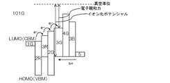
- FIG. 3 is an energy level diagram of an example of each layer in the red light emitting region of the light emitting device according to the first embodiment.
- FIG. 3 is an energy level diagram of an example of each layer in the green light emitting region of the light emitting device according to the first embodiment.
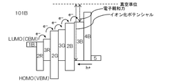
- FIG. 3 is an energy level diagram of an example of each layer in the blue light emitting region of the light emitting device according to the first embodiment.
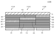
- FIG. 1 is a diagram schematically showing an example of a laminated structure of a light emitting device 100A according to the present embodiment.
- the light emitting device 100A is a device that emits light.
- the light emitting device 100A may be, for example, a lighting device (for example, a backlight or the like) that emits light such as white light, or displays an image (for example, including character information or the like) by emitting light. It may be a display device.
- a display device In this embodiment, an example in which the light emitting device 100A is one pixel in the display device will be described.
- a display device can be configured by arranging a plurality of pixels in a matrix.
- the light emitting device 100A includes, for example, a red light emitting region (first light emitting region) 101R, a green light emitting region (second light emitting region) 101G, and a blue light emitting region (third light emitting region) 101B.
- the red emission region 101R has a emission center wavelength of the first wavelength, and emits light at, for example, about 630 nm.
- the green light emitting region 101G is a second wavelength in which the emission center wavelength is shorter than the first wavelength, and is, for example, about 530 nm.
- the blue light emitting region 101B is a third wavelength in which the emission center wavelength is shorter than the second wavelength, and is, for example, about 440 nm.
- the red light emitting region 101R is a region that emits red light in the light emitting device 100A.
- the red light emitting region 101R corresponds to, for example, the red light emitting element in the light emitting device 100A.
- the cathode 1R, the second electron transport layer 2R, the first light emitting layer 3R, the first electron block layer 4R, the second light emitting layer 3G, the third light emitting layer 3B, and the anode 5 are laminated in this order. It has a structure that has been constructed. That is, in the red light emitting region 101R, each layer is arranged between the cathode 1R and the anode 5 arranged so as to face the cathode 1R.
- the cathode 1R for example, injects electrons into the first light emitting layer 3R.
- the anode 5 injects holes into the first light emitting layer 3R, for example.
- the cathode 1R and the anode 5 are made of a conductive material such as a metal, a transparent conductive oxide, or a conductive nanomaterial.
- a conductive material such as a metal, a transparent conductive oxide, or a conductive nanomaterial.
- the metal include alloys such as Al, Cu, Au, Ag and MgAg.
- the transparent conductive oxide include indium tin oxide (ITO), indium zinc oxide (IZO), zinc oxide (ZnO), aluminum zinc oxide (ZnO: Al (AZO)), and boron zinc oxide. (ZnO: B (BZO)) and the like.
- the conductive nanomaterial include Ag nanowires, carbon nanotubes, ITO nanoparticles and the like.
- the cathode 1R and the anode 5 may be, for example, a laminate including at least one metal layer and / or at least one transparent conductive oxide layer.
- the first light emitting layer 3R is arranged between the cathode 1R and the anode 5.
- the first light emitting layer 3R has a light emitting center wavelength of the first wavelength, and emits light at, for example, about 630 nm.
- the first light emitting layer 3R includes, for example, a first light emitting material having a light emitting center wavelength of the first wavelength and emitting light at, for example, about 630 nm.
- the first light emitting material emits light, for example, by recombination of the injected electrons and the injected holes. That is, it can be said that the first light emitting layer 3R emits light by recombination of the injected electrons and the injected holes, for example.
- the first light emitting layer 3R in the present embodiment for example, as shown in FIG. 6, holes (from the anode 5 through the third light emitting layer 3B, the second light emitting layer 3G, and the first electron block layer 4R) ( h +) is injected.
- holes from the anode 5 through the third light emitting layer 3B, the second light emitting layer 3G, and the first electron block layer 4R
- h + is injected.
- electrons (e ⁇ ) are injected from the cathode 1R via the second electron transport layer 2R.
- the emission center wavelength represents, for example, an emission peak in the emission layer.
- the electron affinity in the first light emitting layer 3R is the energy level of LUMO when the first light emitting layer 3R is an organic material, or the case where the first light emitting layer 3R is an inorganic crystal material. Corresponds to the magnitude required to extract an electron from the energy level of CBM to the vacuum level.
- the ionization potential of the first light emitting layer 3R is based on the energy level of HOMO when the first light emitting layer 3R is an organic material or the energy level of VBM when the first light emitting layer 3R is an inorganic crystal material. It is the size required to extract electrons to the vacuum level, and corresponds to the value obtained by adding the band gap to the electron affinity.
- the first light emitting layer 3R has been described, but the same applies to the other layers.
- Examples of the first light emitting material include quantum dots.
- Quantum dots are, for example, semiconductor fine particles having a particle size of 100 nm or less, and are MgS, MgSe, MgTe, MgZnS, MgZnSe, CaS, CaSe, CaTe, SrS, SrSe, SrTe, BaS, BaSe, BaTe, ZnS, ZnSe, etc.
- the II-VI group semiconductor compounds such as ZnTe, ZnSSe, ZnTeS, ZnTeSe, CdS, CdSe, CdSSe, CdTe, CdSeTe, CdZnSe, CdZnTe, HgS, HgSe, HgTe, and / or GaAs, GaP, InN, In It can have a crystal of a group III-V semiconductor compound such as InSb and / or a crystal of a group IV semiconductor compound such as Si and Ge.
- the quantum dots may have, for example, a core / shell structure in which the above semiconductor crystal is used as a core and the core is overcoated with a shell material having a high bandgap.
- the second electron transport layer 2R is arranged between the cathode 1R and the first light emitting layer 3R.
- the second electron transport layer 2R transports the electrons injected from the cathode 1R to the first light emitting layer 3R.
- the energy level of the LUMO (Lowest Unoccupied Molecular Orbital) of the second electron transport layer 2R is lower than the energy level of the LUMO of the first light emitting layer 3R.
- the electrons injected from the cathode 1R can be easily transported to the first light emitting layer 3R via the second electron transport layer 2R.
- the energy level of the HOMO (Highest Occupied Molecular Orbital) of the second electron transport layer 2R is lower than the energy level of the HOMO of the first light emitting layer 3R.
- the energy level of the HOMO (Highest Occupied Molecular Orbital) of the second electron transport layer 2R is lower than the energy level of the HOMO of the first light emitting layer 3R.
- Examples of the material forming the second electron transport layer 2R include zinc oxide (for example, ZnO), titanium oxide (for example, TiO 2 ), strontium oxide titanium (for example, SrTiO 3 ), In 2 O 3 , CdS, LZO, and SiTe. Electron-transporting materials such as SiSe, SiS, fullerene derivatives, and In 2 O 3 are used. Only one kind of these electron transporting materials may be used, or two or more kinds may be mixed and used as appropriate. The material forming the second electron transport layer 2R is appropriately selected according to the energy level of HOMO and the energy level of LUMO of each layer.
- the first electron block layer 4R is arranged between the first light emitting layer 3R and the second light emitting layer 3G.
- the first electron block layer 4R blocks the injection of electrons injected from the cathode 1R into the second light emitting layer 3G side.
- the energy level of LUMO of the first electron block layer 4R is higher than the energy level of LUMO of the first light emitting layer 3R.
- the energy level of LUMO of the first electron block layer 4R is higher than the energy level of LUMO of the first light emitting layer 3R.
- the energy level of HOMO of the first electron block layer 4R is equal to or higher than the energy level of HOMO of the first light emitting layer 3R.
- the holes injected from the anode 5 can be more easily injected into the first light emitting layer 3R.
- the material for forming the first electron block layer 4R is, for example, any one of Zn, Cr, Ni, Ti, Nb, Al, Si, Mg, Ta, Hf, Zr, Y, La, and Sr.
- TFB Second butylphenyl imino) -1,4-phenylene
- Poly-TPD poly (triphenylamine) derivative
- Poly-TPD poly (3,4-ethylenedioxythiophene) / poly (4-styrenesulfonic acid
- Examples thereof include a hole-transporting organic material such as (PEDOT-PSS).
- the material forming the first electron block layer 4R is appropriately adjusted to the HOMO energy level and LUMO energy level of each layer. Be selected.
- the second light emitting layer 3G has a emission center wavelength of the second wavelength, and emits light at, for example, about 530 nm.
- the second light emitting layer 3G includes, for example, a second light emitting material having a light emitting center wavelength of the second wavelength and emitting light at, for example, about 530 nm.
- the second light emitting material emits light, for example, by recombination of the injected electrons and the injected holes. That is, it can be said that the second light emitting layer 3G emits light by, for example, recombination of the injected electrons and the injected holes.
- Examples of the second light emitting material include quantum dots similar to those of the first light emitting material.
- the diameter of the quantum dots is smaller in the second light emitting material, and the band gap becomes wider due to the quantum effect.
- the energy level of the conduction band becomes shallower and the level of the valence band becomes deeper, but the level of the valence band changes.
- the change in the level of the conduction band is larger than that of.
- the second light emitting material is appropriately selected according to the energy level of HOMO and the energy level of LUMO of each layer.
- the energy level of LUMO is higher than the energy level of LUMO of the first light emitting layer 3R.
- the holes injected from the anode 5 can be more easily injected into the first light emitting layer 3R via the second light emitting layer 3G.
- the electrons injected from the cathode 1R are blocked by the first electron block layer 4R arranged between the second light emitting layer 3G and the cathode 1R. Therefore, almost no electrons are injected. Therefore, in the second light emitting layer 3G, the holes injected from the anode 5 and the electrons injected from the cathode 1R are hardly recombined and hardly emit light.
- the third light emitting layer 3B is arranged between the anode 5 and the second light emitting layer 3G.
- the third light emitting layer 3B has a emission center wavelength of the third wavelength, and emits light at, for example, about 440 nm.
- the third light emitting layer 3B contains, for example, a third light emitting material having a light emitting center wavelength of the third wavelength and emitting light at, for example, about 440 nm.
- the third light emitting material emits light, for example, by recombination of the injected electrons and the injected holes. That is, it can be said that the second light emitting layer 3G emits light by, for example, recombination of the injected electrons and the injected holes.
- Examples of the third light emitting material include quantum dots similar to those of the first light emitting material.
- the third light emitting material is appropriately selected according to the energy level of HOMO and the energy level of LUMO of each layer.
- the energy level of LUMO is higher than the energy level of LUMO of the second light emitting layer 3G.
- the holes injected from the anode 5 are easily transferred to the first light emitting layer 3R via the third light emitting layer 3B, the second light emitting layer 3G, and the first electron block layer 4R. Can be injected into.
- the third light emitting layer 3B may be arranged so as to be in direct contact with the second light emitting layer 3G.
- the electrons injected from the cathode 1R are blocked by the first electron block layer 4R arranged between the third light emitting layer 3B and the cathode 1R, so that the electrons are substantially injected. Not done. Therefore, in the third light emitting layer 3B, the holes injected from the anode 5 and the electrons injected from the cathode 1R cannot be recombined, and almost no light is emitted.
- the first light emitting layer 3R emits light
- the second light emitting layer 3G and the third light emitting layer 3B emit almost no light, so that the light emitting center wavelength emits light at the first wavelength.
- the green light emitting region 101G is a region that emits green light in the light emitting device 100A.
- the green light emitting region 101G corresponds to, for example, a green light emitting element in the light emitting device 100A.
- the anode 5 has a structure in which the anodes 5 are laminated in this order.
- each layer is arranged between the cathode 1G and the anode 5 arranged so as to face the cathode 1G.
- the cathode 1G can be made of the same material as the cathode 1R by injecting electrons into the second light emitting layer 3G.
- the cathode 1R is used as the cathode 1G, the first electron block layer 4R is not provided, and the cathode 1R is between the first light emitting layer 3R and the second light emitting layer 3G.
- the first electron transport layer 2G is arranged, and the second electron block layer 4G is further arranged between the second light emitting layer 3G and the third light emitting layer 3B.
- the first electron transport layer 2G transports electrons injected from the cathode 1G to the second light emitting layer 3G.
- the energy level of LUMO is located between the energy level of LUMO of the first light emitting layer 3R and the energy level of LUMO of the second light emitting layer 3G.
- the electrons injected from the cathode 1G are transferred to the second light emitting layer 3G via the second electron transport layer 2R, the first light emitting layer 3R, and the first electron transport layer 2G. Injection can be made easier.
- the energy level of HOMO of the first electron transport layer 2G is lower than the energy level of HOMO of the second light emitting layer 3G.
- the holes injected from the anode 5 are transferred to the first light emitting layer 3R via the third light emitting layer 3B, the second electron block layer 4G, and the second light emitting layer 3G.
- the infusion can be blocked.
- the holes injected from the anode 5 can be confined in the second light emitting layer 3G, the luminous efficiency in the green light emitting region 101G can be improved.
- the material for forming the first electron transport layer 2G for example, TPBi and ZrO 2 can be used in addition to the same material as the second electron transport layer 2R.
- the material forming the first electron transport layer 2G is appropriately selected according to the energy level of HOMO and the energy level of LUMO of each layer.
- the first electron transport layer 2G blocks the injection of holes into the first light emitting layer 3R, so that the first light emitting layer 3R hardly emits light.
- the second electron block layer 4G is arranged between the first light emitting layer 3R and the second light emitting layer 3G.
- the second electron block layer 4G blocks the injection of electrons injected from the cathode 1G into the third light emitting layer 3B side.
- the LUMO energy level of the second electron block layer 4G is higher than the LUMO energy level of the second light emitting layer 3G.
- the LUMO energy level of the second electron block layer 4G is higher than the LUMO energy level of the second light emitting layer 3G.
- the energy level of HOMO of the second electron block layer 4G is equal to or higher than the energy level of HOMO of the second light emitting layer 3G. This makes it easier, for example, to inject the holes injected from the anode 5 into the second light emitting layer 3G via the third light emitting layer 3B and the second electron block layer 4G, as shown in FIG. 7. be able to.
- the same material as the first electron block layer 4R can be used.
- the material forming the second electron block layer 4G is appropriately selected according to the energy level of HOMO and the energy level of LUMO of each layer.
- the second electron block layer 4G blocks the injection of electrons injected from the cathode 1G into the third light emitting layer 3B, so that the third light emitting layer 3B hardly emits light. ..
- the second light emitting layer 3G emits light
- the first light emitting layer 3R and the third light emitting layer 3B emit almost no light, so that the light emitting center wavelength emits light at the second wavelength.
- the blue light emitting region 101B is a region that emits blue light in the light emitting device 100A.
- the blue light emitting region 101B corresponds to, for example, a blue light emitting element in the light emitting device 100A.
- the three-electron block layer 4B and the anode 5 are laminated in this order.
- each layer is arranged between the cathode 1B and the anode 5 arranged so as to face the cathode 1B.
- the cathode 1B can be made of the same material as the cathode 1R by injecting electrons into the third light emitting layer 3B.
- the first light emitting layer 3R and the second light emitting layer 3G may be arranged so as to be in direct contact with each other.
- the cathode 1G is used as the cathode 1B, the second electron block layer 4G is not provided, and the second light emitting layer 3G and the third light emitting layer 3B are separated from each other.
- the third electron transport layer 2B is arranged, and the third electron block layer 4B is further arranged between the third light emitting layer 3B and the anode 5.
- the third electron transport layer 2B transports the electrons injected from the cathode 1B to the third light emitting layer 3B.
- the energy level of LUMO is located between the energy level of LUMO of the second light emitting layer 3G and the energy level of LUMO of the third light emitting layer 3B.
- the electrons injected from the cathode 1B are passed through the second electron transport layer 2R, the first light emitting layer 3R, the first electron transport layer 2G, and the second light emitting layer 3G. , Can be easily injected by the third light emitting layer 3B.
- the energy level of HOMO of the third electron transport layer 2B is lower than the energy level of HOMO of the third light emitting layer 3B.
- the holes injected from the anode 5 can be blocked from being injected into the second light emitting layer 3G via the third electron block layer 4B and the third light emitting layer 3B. can.
- the holes injected from the anode 5 can be confined in the third light emitting layer 3B, the luminous efficiency in the blue light emitting region 101B can be improved.
- the material for forming the third electron transport layer 2B for example, Bphen and TAZ can be used in addition to the same material as the first electron transport layer 2G.
- the material forming the third electron block layer 2B is appropriately selected according to the energy level of HOMO and the energy level of LUMO of each layer. As described above, in the blue light emitting region 101B, since the injection of holes into the second light emitting layer 3G is blocked by the third electron transport layer 2B, the second light emitting layer 3G hardly emits light.
- the third electron block layer 4B is arranged between the anode 5 and the third light emitting layer 3B.
- the third electron block layer 4B blocks the passage of electrons injected from the cathode 1G through the third light emitting layer 3B. It is preferable that the energy level of LUMO of the third electron block layer 4B is higher than the energy level of LUMO of the third light emitting layer 3B.
- the electrons are injected from the cathode 1B, and the second electron transport layer 2R, the first light emitting layer 3R, the first electron transport layer 2G, the second light emitting layer 3G, and the third electron transport layer 2B. Since the electrons injected into the third light emitting layer 3B can be confined in the third light emitting layer 3B, the luminous efficiency in the blue light emitting region 101B can be improved.
- the energy level of HOMO of the third electron block layer 4B is equal to or higher than the energy level of HOMO of the third light emitting layer 3B.
- the holes injected from the anode 5 can be easily injected by the third light emitting layer 3B.
- the cathodes 1R, 1G, and 1R in the present embodiment correspond to the pixel electrodes of the light emitting device 100A, and it is preferable that they are insulated from each other in each light emitting region.
- the cathodes 1R, 1G, and 1R can be referred to as a first portion, a second portion, and a third portion of the cathode in the light emitting device 100A.
- the anode 5 in the present embodiment corresponds to the common electrode of the light emitting device 100A, and is formed in common in each light emitting region.
- the configuration of the cathode and the anode in the present embodiment is not limited to this, and for example, the cathode may be the common electrode and the anode may be the pixel electrode. Further, the stacking order of each layer in the present embodiment may be reversed.
- a substrate (not shown) is placed on the surface of the cathode 1 of each light emitting region 101R / 101G / 101B opposite to the surface on which the second electron transport layer 2R is arranged. ) May be arranged.
- the substrate is made of, for example, glass or the like, and functions as a support for supporting each of the above layers.
- the substrate may be, for example, an array substrate on which a thin film transistor (TFT) or the like is formed.
- the third light emitting layer corresponding to the blue light emitting layer having a large band gap and a higher electron injection barrier than the light emitting layers of other colors. It is possible to facilitate injecting electrons between the third light emitting layer 3B and the cathode 1B into the light emitting layer 3B. Thereby, in particular, the luminous efficiency in the third light emitting layer 3B can be improved, and the light emitting balance with the light emitting region of another color can be more easily obtained.
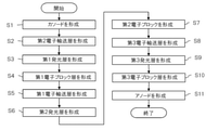
- FIG. 2 is a diagram showing an example of a manufacturing flow of the light emitting device 100A.
- cathodes 1R, 1G, and 1B are formed on the substrate (S1).
- the cathodes 1R, 1G, and 1B are portions corresponding to the red light emitting region 101R, the green light emitting region 101G, and the blue light emitting region 101B after forming a solid layer by various conventionally known methods such as a sputtering method and a vacuum vapor deposition method. It can be formed by patterning by removing other than the above.
- the cathodes 1R, 1G, and 1B may be configured to insulate each other by forming, for example, an insulating layer or the like.
- the second electron transport layer 2R is formed on the cathodes 1R, 1G, and 1B (S2).
- the second electron transport layer 2R can be formed by various conventionally known methods such as vacuum deposition, sputtering, transfer method, inkjet method or coating method.
- the second electron transport layer 2R in the present embodiment is common to the red light emitting region 101R, the green light emitting region 101G, and the blue light emitting region 101B. Therefore, it is not necessary to form each light emitting region, and the manufacturing process of the light emitting device 100A can be reduced.
- the first light emitting layer 3R is formed on the second electron transport layer 2R (S3).
- the first light emitting layer 3R can be formed by various conventionally known methods such as vacuum deposition, sputtering, or a coating method.
- the first light emitting layer 3R in the present embodiment is common to the red light emitting region 101R, the green light emitting region 101G, and the blue light emitting region 101B. Therefore, it is not necessary to form each light emitting region, and the manufacturing process of the light emitting device 100A can be reduced.
- the first electron block layer 4R is formed on the first light emitting layer 3R (S4).
- the first electron block layer 4R has a solid layer formed by various conventionally known methods such as vacuum vapor deposition, sputtering, transfer method, inkjet method or coating method, and then leaves a portion corresponding to the red light emitting region 101R. In other words, it can be patterned and formed so as to remove the portions corresponding to the green light emitting region 101G and the blue light emitting region 101B.
- the first electron transport layer 2G is formed on the first light emitting layer 3R on which the first electron block layer 4R in the red light emitting region 101R is not formed (S5).
- the first electron transport layer 2G forms a solid layer by various conventionally known methods such as vacuum vapor deposition, sputtering, or a coating method, and then leaves a portion corresponding to a green light emitting region 101G and a blue light emitting region 101B. In other words, it can be patterned and formed by removing the portion corresponding to the red light emitting region 101R.
- the first electron transport layer 2G can collectively form the portions corresponding to the green light emitting region 101G and the blue light emitting region 101B, the manufacturing process of the light emitting device 100A can be reduced.
- the order of S4 and S5 may be changed.
- a second light emitting layer 3G is formed on the first electron block layer 4R and the first electron transport layer 2G (S6).
- the second light emitting layer 3G can be formed by various conventionally known methods such as vacuum deposition, sputtering, or a coating method, as in the case of the first light emitting layer 3R, for example.
- the second light emitting layer 3G in the present embodiment is common to the red light emitting region 101R, the green light emitting region 101G, and the blue light emitting region 101B. Therefore, it is not necessary to form each light emitting region, and the manufacturing process of the light emitting device 100A can be reduced.
- a second electron block layer 4G is formed on the second light emitting layer 3G (S7).
- the second electron block layer 4G forms a solid layer by various conventionally known methods such as vacuum vapor deposition, sputtering, or a coating method, and then leaves a portion corresponding to the green light emitting region 101G, in other words, red light emission. It can be formed by patterning so as to remove the portion corresponding to the region 101R and the blue light emitting region 101B.
- the third electron transport layer 2B is formed on the second light emitting layer 3G on which the second electron block layer 4G is not formed in the blue light emitting region 101B (S8).
- the third electron transport layer 2B forms a solid layer by various conventionally known methods such as, for example, vacuum vapor deposition, sputtering, or a coating method, and then leaves a portion corresponding to the blue light emitting region 101B, in other words. It can be patterned and formed by removing the portions corresponding to the red light emitting region 101R and the green light emitting region 101G.
- a third light emitting layer 3B is formed on the second light emitting layer 3G in the red light emitting region 101R, the second electron block layer 4G in the green light emitting region 101G, and the third electron transporting layer 2B in the blue light emitting region 101B (S9).
- the third light emitting layer 3B can be formed by various conventionally known methods such as vacuum deposition, sputtering, or a coating method.
- the third light emitting layer 3B in the present embodiment is common to the red light emitting region 101R, the green light emitting region 101G, and the blue light emitting region 101B. Therefore, it is not necessary to form each light emitting region, and the manufacturing process of the light emitting device 100A can be reduced.
- a third electron block layer 4B is formed on the third light emitting layer 3B (S10).
- the third electron block layer 4B forms a solid layer by various conventionally known methods such as, for example, vacuum deposition, sputtering, or a coating method, and then leaves a portion corresponding to the blue light emitting region 101B, in other words, red. It can be patterned and formed by removing the portions corresponding to the light emitting region 101R and the green light emitting region 101G.
- the anode 5 is formed on the third light emitting layer 3B in the red light emitting region 101R and the green light emitting region 101G, and the third electron block layer 4B in the blue light emitting region 101B (S11).
- the anode 5 can be formed by various conventionally known methods such as vacuum deposition, sputtering, or a coating method.
- the anode 5 in this embodiment is common to the red light emitting region 101R, the green light emitting region 101G, and the blue light emitting region 101B. Therefore, it is not necessary to form each light emitting region, and the manufacturing process of the light emitting device 100A can be reduced.
- the light emitting device 100A can be manufactured.
- FIG. 3 is a diagram schematically showing an example of the laminated structure of the light emitting device 100B according to the present embodiment.
- the second electron transport layer 2R is not formed in the green light emitting region 101G, and the second electron transport layer 2R and the first electron transport layer 2R are formed in the blue light emitting region 101B.
- the structure is such that the electron transport layer 2G is not formed.
- the second electron transport layer 2R is patterned so as to remove the portions corresponding to the green light emitting region 102G and the blue light emitting region 102B in S2 in the first embodiment. , Can be formed.
- the first electron transport layer 2G is patterned so as to remove the portion corresponding to the blue light emitting region 102B in addition to the portion corresponding to the red light emitting region 101R in S5 in the first embodiment. , Can be formed.
- the number of layers formed in the red light emitting region 101R, the green light emitting region 102G, and the blue light emitting region 102B can be made equal.
- FIG. 4 is a diagram schematically showing an example of the laminated structure of the light emitting device 100C according to the present embodiment.
- the light emitting device 100C has a configuration in which a bank 6 for partitioning a red light emitting region 101R, a green light emitting region 101G, and a blue light emitting region 101B is formed in the light emitting device 100A according to the first embodiment.
- the bank 6 may be formed between S1 and S2 in the first embodiment.
- the inkjet method can be used when forming each layer by using a solution or the like in S2 to S10 in the first embodiment.
- the red light emitting region 103R, the green light emitting region 103G, and the blue light emitting region 102B are partitioned by the bank 6, color mixing in each region can be suppressed.
- FIG. 5 is a diagram schematically showing an example of the laminated structure of the light emitting device 100D according to the present embodiment.
- the second electron block layer 4G and the third electron block layer 4B are formed in the red light emitting region 101R, and the third electron block layer is formed in the green light emitting region 101G. It is a configuration in which 4B is formed.
- the second electron block layer 4G leaves a portion corresponding to the red light emitting region 104R in addition to the portion corresponding to the green light emitting region 104G in the second electron block layer in S7 in the first embodiment. It can be formed by patterning in such a manner.
- the third electron block layer 4B does not have to pattern the third electron block layer in S10 in the first embodiment.
- the number of layers formed in the red light emitting region 104R, the green light emitting region 104G, and the blue light emitting region 101B can be made equal. As a result, it becomes easy to make the thicknesses in the red light emitting region 104R, the green light emitting region 104G, and the blue light emitting region 101B uniform, and it becomes easy to balance the light emitting intensity among the respective light emitting regions.
- the present invention is not limited to the above-described embodiment, but is substantially the same as the configuration shown in the above-described embodiment, a configuration having the same action and effect, or a configuration capable of achieving the same object. May be replaced with.
- each layer is an organic material
- the heights of the HOMO energy level and the LUMO energy level in each layer are compared.
- the energy level of HOMO and the energy level of LUMO in each layer are set to the lower end (CBM) of the conduction band in each layer, respectively. It can be replaced with the energy level and the energy level at the top of the valence band (VBM).
- VBM valence band
- each layer is composed of an organic material and an inorganic crystalline material
- the energy level of HOMO and the energy level of LUMO in each layer can be replaced with the magnitudes of ionization potential and electron affinity in each layer, respectively.
- the magnitude of the energy required to extract electrons from the LUMO energy level in an organic material or the CBM energy level in an inorganic crystalline material to a vacuum order is the electron affinity, and the HOMO energy level in an organic material.
- the magnitude of the energy required to extract electrons from the energy level of VBM in the inorganic crystal material to the vacuum level is the value obtained by adding the band gap to the electron affinity, that is, the ionization potential.
Landscapes
- Physics & Mathematics (AREA)
- Optics & Photonics (AREA)
- Electroluminescent Light Sources (AREA)
Abstract
発光装置は、発光中心波長が第1波長である第1発光領域と、発光中心波長が前記第1波長よりも短波長である第2波長である第2発光領域と、を含み、前記第1発光領域及び前記第2発光領域に配されたカソードと、前記第1発光領域及び前記第2発光領域において前記カソードと対向するように配されたアノードと、前記カソードと前記アノードとの間に配されており、発光中心波長が前記第1波長である第1発光層と、少なくとも前記第2発光領域において前記アノードと前記第1発光層との間に配されており、発光中心波長が前記第2波長であり、電子親和力が前記第1発光層の電子親和力よりも小さい第2発光層と、前記第2発光領域において前記第1発光層と前記第2発光層との間に配されており、電子親和力が、前記第1発光層の電子親和力と、前記第2発光層の電子親和力との間の大きさの第1電子輸送層と、を備える。
Description
本発明は、発光装置に関する。
例えば、特許文献1には、アノード、第1発光層、第2発光層、カソードがこの順で積層された発光装置が開示されている。そして、第1発光層は、その一部が処理されて非発光化されることにより、発光領域と非発光領域に分割されている。
特許文献1に記載の発光装置では、第1発光層の非発光領域と、第2発光層とが積層された構造となっており、アノードから供給される正孔が第1発光層の非発光領域を介して第2発光層に至ることにより、第2発光層で発光する。上記発光装置においては、第1発光層の非発光領域が、第2発光層に至る正孔をブロックする場合があり、発光効率が低下し得る。
本開示の主な目的は、例えば、発光効率の低下を抑制することができる発光装置を提供することにある。
本開示の主な目的は、例えば、発光効率の低下を抑制することができる発光装置を提供することにある。
本発明の一形態の発光装置は、発光中心波長が第1波長である第1発光領域と、発光中心波長が前記第1波長よりも短波長である第2波長である第2発光領域と、を含み、前記第1発光領域及び前記第2発光領域に配されたカソードと、前記第1発光領域及び前記第2発光領域において前記カソードと対向するように配されたアノードと、前記カソードと前記アノードとの間に配されており、発光中心波長が前記第1波長である第1発光層と、少なくとも前記第2発光領域において前記アノードと前記第1発光層との間に配されており、発光中心波長が前記第2波長であり、電子親和力が前記第1発光層の電子親和力よりも小さい第2発光層と、前記第2発光領域において前記第1発光層と前記第2発光層との間に配されており、電子親和力が、前記第1発光層の電子親和力と、前記第2発光層の電子親和力との間の大きさの第1電子輸送層と、を備える。
以下、本発明を実施した好ましい形態の一例について説明する。但し、下記の実施形態は、単なる例示である。本発明は、下記の実施形態に何ら限定されない。
〔実施形態1〕
図1は、本実施形態に係る発光装置100Aの積層構造の一例を模式的に示す図である。
図1は、本実施形態に係る発光装置100Aの積層構造の一例を模式的に示す図である。
発光装置100Aは、光を出射する装置である。発光装置100Aは、例えば、白色光等の光を出射する照明装置(例えば、バックライト等)であってもよいし、光を出射することにより画像(例えば、文字情報等を含む。)を表示する表示装置であってもよい。本実施形態では、発光装置100Aが、表示装置における1つの画素である例について説明する。例えば、複数の画素をマトリクス状に配列することにより表示装置を構成することができる。
図1に示すように、発光装置100Aは、例えば、赤色発光領域(第1発光領域)101R、緑色発光領域(第2発光領域)101G、青色発光領域(第3発光領域)101Bを含む。赤色発光領域101Rは、発光中心波長が第1波長であり、例えば約630nmで発光する。緑色発光領域101Gは、発光中心波長が第1波長よりも短波長である第2波長であり、例えば約530nmである。青色発光領域101Bは、発光中心波長が第2波長よりも短波長である第3波長であり、例えば、約440nmである。
赤色発光領域101Rは、発光装置100Aにおいて赤色に発光する領域である。赤色発光領域101Rは、例えば、発光装置100Aにおける赤色発光素子に相当する。赤色発光領域101Rにおいては、カソード1R、第2電子輸送層2R、第1発光層3R、第1電子ブロック層4R、第2発光層3G、第3発光層3B、およびアノード5が、この順に積層された構造となっている。つまり、赤色発光領域101Rにおいては、カソード1Rと、カソード1Rに対向するように配されたアノード5との間に、各層が配された構造となっている。
カソード1Rは、例えば、第1発光層3Rに電子を注入する。
アノード5は、例えば、第1発光層3Rに正孔を注入する。
カソード1Rおよびアノード5は、例えば、金属や透明導電性酸化物や導電性ナノ材料等の導電材料により構成される。上記金属としては、例えば、Al、Cu、Au、AgやMgAgなどの合金等が挙げられる。上記透明導電性酸化物としては、例えば、インジウムスズ酸化物(ITO)、インジウム亜鉛酸化物(IZO)、酸化亜鉛(ZnO)、アルミニウム亜鉛酸化物(ZnO:Al(AZO))、ホウ素亜鉛酸化物(ZnO:B(BZO))等が挙げられる。導電ナノ材料としては、Agナノワイヤー、カーボンナノチューブやITOナノ粒子等が挙げられる。なお、カソード1Rおよびアノード5は、例えば、少なくとも1層の金属層および/または少なくとも1層の透明導電性酸化物層を含む積層体であってもよい。
第1発光層3Rは、カソード1Rとアノード5との間に配されている。第1発光層3Rは、発光中心波長が第1波長であり、例えば約630nmで発光する。第1発光層3Rは、例えば、発光中心波長が第1波長であり、例えば約630nmで発光する第1発光材料を含む。第1発光材料は、例えば、注入された電子と、注入された正孔との再結合により発光する。つまり、第1発光層3Rは、例えば、注入された電子と、注入された正孔との再結合により発光するということができる。なお、本実施形態における第1発光層3Rにおいては、例えば、図6に示すように、アノード5から第3発光層3B、第2発光層3Gおよび第1電子ブロック層4Rを介して正孔(h+)が注入される。一方、本実施形態における第1発光層3Rにおいては、例えば、図6に示すように、カソード1Rから第2電子輸送層2Rを介して電子(e-)が注入される。また、上記発光中心波長とは、例えば、発光層における発光ピークを表すものである。さらに、図6に示すように、第1発光層3Rにおける電子親和力は、第1発光層3Rが有機材料である場合のLUMOのエネルギー準位、もしくは第1発光層3Rが無機結晶材料である場合のCBMのエネルギー準位から電子を真空準位に取り出すのに必要な大きさに相当する。また、第1発光層3Rにおけるイオン化ポテンシャルは、第1発光層3Rが有機材料である場合のHOMOのエネルギー準位、もしくは第1発光層3Rが無機結晶材料である場合のVBMのエネルギー準位から電子を真空準位に取り出すのに必要な大きさであり、電子親和力にバンドギャップを加えた値に相当する。ここでは、第1発光層3Rについて説明したが、他の層においても同様である。
第1発光材料としては、例えば、量子ドット等が挙げられる。量子ドットは、例えば、100nm以下の粒子サイズを有する半導体微粒子であり、MgS、MgSe、MgTe、MgZnS、MgZnSe、CaS、CaSe、CaTe、SrS、SrSe、SrTe、BaS、BaSe、BaTe、ZnS、ZnSe、ZnTe、ZnSSe、ZnTeS、ZnTeSe、CdS、CdSe、CdSSe、CdTe、CdSeTe、CdZnSe、CdZnTe、HgS、HgSe、HgTe等のII-VI族半導体化合物、及び/又は、GaAs、GaP、InN、InAs、InP、InSb等のIII-V族半導体化合物の結晶、及び/又は、Si、Ge等のIV族半導体化合物の結晶を有することができる。また、量子ドットは、例えば、上記の半導体結晶をコアとして、当該コアをバンドギャップの高いシェル材料でオーバーコートしたコア/シェル構造を有していてもよい。更に、量子ドットは、APbX3[A=Cs,MA(メチルアンモニウム),FA(ホルムアミジニウム),X=Cl,Br,I]、(CH3NH3)3Bi2X9などのペロブスカイト構造を有していてもよい。
第2電子輸送層2Rは、カソード1Rと第1発光層3Rとの間に配されている。第2電子輸送層2Rは、カソード1Rから注入される電子を第1発光層3Rに輸送する。
第2電子輸送層2Rは、LUMO(Lowest Unoccupied Molecular Orbital)のエネルギー準位が第1発光層3RのLUMOのエネルギー準位よりも低いことが好ましい。これにより、例えば、図6に示すように、カソード1Rから注入される電子を第2電子輸送層2Rを介して第1発光層3Rに容易に輸送することができる。
さらに、第2電子輸送層2Rは、HOMO(Highest Occupied Molecular Orbital)のエネルギー準位が、第1発光層3RのHOMOのエネルギー準位よりも低いことが好ましい。これにより、例えば、図6に示すように、アノード5から、第3発光層3、第2発光層3Gおよび第1電子ブロック層4Rを介して注入された正孔を第1発光層3Rにより閉じ込めることができ、赤色発光領域101Rにおける発光効率を向上させることができる。
第2電子輸送層2Rを形成する材料としては、例えば、酸化亜鉛(例えばZnO)、酸化チタン(例えばTiO2)、酸化ストロンチウムチタン(例えばSrTiO3)、In2O3、CdS、LZO、SiTe、SiSe、SiS、フラーレン誘導体、In2O3等の電子輸送性材料が用いられる。これら電子輸送性材料は、一種類のみを用いてもよく、適宜、二種類以上を混合して用いてもよい。なお、第2電子輸送層2Rを形成する材料は、各層のHOMOのエネルギー準位、LUMOのエネルギー準位に合わせて、適宜選択される。
第1電子ブロック層4Rは、第1発光層3Rと第2発光層3Gとの間に配されている。第1電子ブロック層4Rは、カソード1Rから注入される電子の、第2発光層3G側への注入をブロックする。
さらに、第1電子ブロック層4Rは、LUMOのエネルギー準位が、第1発光層3RのLUMOのエネルギー準位よりも高いことが好ましい。これにより、例えば、図6に示すように、カソード1Rから第1発光層3Rを介して注入される電子の、第2発光層3G側への注入をより容易にブロックすることができる。さらに、第1発光層3Rに注入された電子を第1発光層3Rに閉じ込めることができるため、赤色発光領域101Rにおける発光効率を向上させることができる。
第1電子ブロック層4Rは、HOMOのエネルギー準位が、第1発光層3RのHOMOのエネルギー準位以上であることが好ましい。これにより、例えば、図6に示すように、アノード5から注入される正孔の、第1発光層3Rへの注入をより容易にすることができる。
第1電子ブロック層4Rを形成する材料としては、例えば、例えば、Zn、Cr、Ni、Ti、Nb、Al、Si、Mg、Ta、Hf、Zr、Y、La、Srのうちのいずれか1つ以上を含む酸化物、窒化物、または炭化物からなる群から選択される一種以上を含む材料や、4,4´,4´´-トリス(9-カルバゾイル)トリフェニルアミン(TCTA)、4,4´-ビス[N-(1-ナフチル)-N-フェニル-アミノ]-ビフェニル(NPB)、亜鉛フタロシアニン(ZnPC)、ジ[4-(N,N-ジトリルアミノ)フェニル]シクロヘキサン(TAPC)、4,4´-ビス(カルバゾ-ル-9-イル)ビフェニル(CBP)、2,3,6,7,10,11-ヘキサシアノ-1,4,5,8,9,12-ヘキサアザトリフェニレン(HATCN)、MoO3などの材料や、ポリ(N-ビニルカルバゾール)(PVK)、ポリ(2,7-(9,9-ジ-n-オクチルフルオレン)-(1,4-フェニレン-((4-第2ブチルフェニル)イミノ)-1,4-フェニレン(TFB)、ポリ(トリフェニルアミン)誘導体(Poly-TPD)、ポリ(3,4-エチレンジオキシチオフェン)/ポリ(4-スチレンスルホン酸)(PEDOT-PSS)などの正孔輸送性有機材料等が挙げられる。なお、第1電子ブロック層4Rを形成する材料は、各層のHOMOのエネルギー準位、LUMOのエネルギー準位に合わせて、適宜選択される。
第2発光層3Gは、発光中心波長が第2波長であり、例えば約530nmで発光する。第2発光層3Gは、例えば、発光中心波長が第2波長であり、例えば約530nmで発光する第2発光材料を含む。第2発光材料は、例えば、注入された電子と、注入された正孔との再結合により発光する。つまり、第2発光層3Gは、例えば、注入された電子と、注入された正孔との再結合により発光するということができる。第2発光材料としては、例えば、第1発光材料と同様の量子ドット等が挙げられる。第1発光材料と第2発光材料が同一組成量子ドットの材料の場合、第2発光材料の方が量子ドットの径が小さく、量子効果によりバンドギャップが広くなる。一般的に、同一材料の量子ドットにおいて、直径が変わり、バンドギャップが変わると、伝導帯のエネルギー準位が浅くなり、価電子帯の準位が深くなるが、価電子帯の準位の変化に比べ伝導帯の準位の変化の方が大きい。なお、第2発光材料は、各層のHOMOのエネルギー準位、LUMOのエネルギー準位に合わせて、適宜選択される。
また、第2発光層3Gは、LUMOのエネルギー準位が第1発光層3RのLUMOのエネルギー準位よりも高い。これにより、例えば、図6に示すように、アノード5から注入された正孔の、第2発光層3Gを介した第1発光層3Rへの注入をより容易にすることができる。
ただし、赤色発光領域101Rにおいては、上記のように、第2発光層3Gには、カソード1Rとの間に配された第1電子ブロック層4Rにより、カソード1Rから注入される電子がブロックされるため、電子がほぼ注入されない。そのため、第2発光層3Gにおいては、アノード5から注入された正孔とカソード1Rから注入された電子がほぼ再結合せず、ほぼ発光しない。
第3発光層3Bは、アノード5と第2発光層3Gとの間に配されている。第3発光層3Bは、発光中心波長が第3波長であり、例えば約440nmで発光する。第3発光層3Bは、例えば、発光中心波長が第3波長であり、例えば約440nmで発光する第3発光材料を含む。第3発光材料は、例えば、注入された電子と、注入された正孔との再結合により発光する。つまり、第2発光層3Gは、例えば、注入された電子と、注入された正孔との再結合により発光するということができる。第3発光材料としては、例えば、第1発光材料と同様の量子ドット等が挙げられる。なお、第3発光材料は、各層のHOMOのエネルギー準位、LUMOのエネルギー準位に合わせて、適宜選択される。
また、第3発光層3Bは、LUMOのエネルギー準位が第2発光層3GのLUMOのエネルギー準位よりも高い。これにより、例えば、図7に示すように、アノード5から注入された正孔を、第3発光層3B、第2発光層3Gおよび第1電子ブロック層4Rを介して第1発光層3Rにより容易に注入することができる。なお、第3発光層3Bは、第2発光層3Gと直接接するように配されていてよい。
ただし、第3発光層3Bは、赤色発光領域101Rにおいては、カソード1Rとの間に配された第1電子ブロック層4Rにより、カソード1Rから注入される電子がブロックされるため、電子がほぼ注入されない。そのため、第3発光層3Bにおいては、アノード5から注入された正孔とカソード1Rから注入された電子が再結合することができず、ほぼ発光しない。
以上のように、赤色発光領域101Rは、第1発光層3Rが発光し、第2発光層3Gおよび第3発光層3Bがほぼ発光しないため、発光中心波長が第1波長で発光する。
続いて、緑色発光領域101Gについて説明する。
緑色発光領域101Gは、発光装置100Aにおいて緑色に発光する領域である。緑色発光領域101Gは、例えば、発光装置100Aにおける緑色発光素子に相当する。緑色発光領域101Gにおいては、カソード1G、第2電子輸送層2R、第1発光層3R、第1電子輸送層2G、第2発光層3G、第2電子ブロック層4G、第3発光層3B、およびアノード5が、この順に積層された構造となっている。つまり、緑色発光領域101Gにおいては、カソード1Gと、カソード1Gに対向するように配されたアノード5との間に、各層が配された構造となっている。なお、カソード1Gは、第2発光層3Gに電子を注入し、カソード1Rと同じ材質を用いることが可能である。
また、緑色発光領域101Gは、赤色発光領域101Rの構成において、カソード1Rをカソード1Gとするとともに、第1電子ブロック層4Rを設けず、第1発光層3Rと第2発光層3Gとの間に第1電子輸送層2Gが配され、さらに第2発光層3Gと第3発光層3Bとの間に第2電子ブロック層4Gが配された構成となっている。
第1電子輸送層2Gは、カソード1Gから注入される電子を第2発光層3Gに輸送する。第1電子輸送層2Gは、LUMOのエネルギー準位が、第1発光層3RのLUMOのエネルギー準位と、第2発光層3GのLUMOのエネルギー準位との間に位置している。これにより、例えば、図7に示すように、カソード1Gから注入された電子の、第2電子輸送層2R、第1発光層3R及び第1電子輸送層2Gを介した第2発光層3Gへの注入をより容易にすることができる。
さらに、第1電子輸送層2Gは、HOMOのエネルギー準位が、前記第2発光層3GのHOMOのエネルギー準位よりも低いことが好ましい。これにより、例えば、図7に示すように、アノード5から注入された正孔の、第3発光層3B、第2電子ブロック層4Gおよび第2発光層3Gを介した第1発光層3Rへの注入をブロックすることができる。さらにまた、アノード5から注入された正孔を第2発光層3Gに閉じ込めることができるため、緑色発光領域101Gにおける発光効率を向上させることができる。
第1電子輸送層2Gを形成する材料としては、例えば、上記第2電子輸送層2Rと同様の材料に加えTPBi、ZrO2を使用することができる。なお、第1電子輸送層2Gを形成する材料は、各層のHOMOのエネルギー準位、LUMOのエネルギー準位に合わせて、適宜選択される。
上記のように、緑色発光領域101Gにおいては、第1電子輸送層2Gにより第1発光層3Rへの正孔の注入がブロックされるため、第1発光層3Rはほぼ発光しない。
第2電子ブロック層4Gは、第1発光層3Rと第2発光層3Gとの間に配されている。第2電子ブロック層4Gは、カソード1Gから注入される電子の、第3発光層3B側への注入をブロックする。
第2電子ブロック層4Gは、LUMOのエネルギー準位が、第2発光層3GのLUMOのエネルギー準位よりも高いことが好ましい。これにより、例えば、図7に示すように、カソード1Gから、第2電子輸送層2R、第1発光層3R、第1電子輸送層2G、および第2発光層3Gを介して注入される電子の、第3発光層3B側への注入をより容易にブロックすることができる。さらに、第2発光層3Gに注入された電子を第2発光層3Gに閉じ込めることができるため、緑色発光領域101Gにおける発光効率を向上させることができる。
さらに、第2電子ブロック層4Gは、HOMOのエネルギー準位が、第2発光層3GのHOMOのエネルギー準位以上であることが好ましい。これにより、例えば、図7に示すように、アノード5から注入される正孔の、第3発光層3B及び第2電子ブロック層4Gを介した第2発光層3Gへの注入をより容易にすることができる。
第2電子ブロック層4Gを形成する材料としては、例えば、上記第1電子ブロック層4Rと同様の材料を使用することができる。なお、第2電子ブロック層4Gを形成する材料は、各層のHOMOのエネルギー準位、LUMOのエネルギー準位に合わせて、適宜選択される。
上記のように、緑色発光領域101Gにおいては、第2電子ブロック層4Gにより第3発光層3Bへのカソード1Gから注入された電子の注入がブロックされるため、第3発光層3Bはほぼ発光しない。
以上のように、緑色発光領域101Gは、第2発光層3Gが発光し、第1発光層3Rおよび第3発光層3Bがほぼ発光しないため、発光中心波長が第2波長で発光する。
続いて、青色発光領域101Bについて説明する。
青色発光領域101Bは、発光装置100Aにおいて青色に発光する領域である。青色発光領域101Bは、例えば、発光装置100Aにおける青色発光素子に相当する。青色発光領域101Bにおいては、カソード1B、第2電子輸送層2R、第1発光層3R、第1電子輸送層2G、第2発光層3G、第3電子輸送層2B、第3発光層3B、第3電子ブロック層4Bおよびアノード5が、この順に積層された構造となっている。つまり、青色発光領域101Bにおいては、カソード1Bと、カソード1Bに対向するように配されたアノード5との間に、各層が配された構造となっている。なお、カソード1Bは、第3発光層3Bに電子を注入し、カソード1Rと同じ材質を用いることが可能である。また、第1発光層3Rと第2発光層3Gとは直接接するように配されていてよい。
また、青色発光領域101Bは、緑色発光領域101Gの構成において、カソード1Gをカソード1Bとするとともに、第2電子ブロック層4Gを設けず、第2発光層3Gと第3発光層3Bとの間に第3電子輸送層2Bが配され、さらに第3発光層3Bとアノード5との間に第3電子ブロック層4Bが配された構成となっている。
第3電子輸送層2Bは、カソード1Bから注入される電子を第3発光層3Bに輸送する。第3電子輸送層2Bは、LUMOのエネルギー準位が、第2発光層3GのLUMOのエネルギー準位と、第3発光層3BのLUMOのエネルギー準位との間に位置している。これにより、例えば、図8に示すように、カソード1Bから注入された電子を、第2電子輸送層2R、第1発光層3R、第1電子輸送層2G、および第2発光層3Gを介して、第3発光層3Bにより容易に注入することができる。
また、第3電子輸送層2Bは、HOMOのエネルギー準位が、第3発光層3BのHOMOのエネルギー準位よりも低いことが好ましい。これにより、例えば、図8に示すように、アノード5から注入された正孔の、第3電子ブロック層4Bおよび第3発光層3Bを介した第2発光層3Gへの注入をブロックすることができる。さらに、アノード5から注入された正孔を第3発光層3Bに閉じ込めることができるため、青色発光領域101Bにおける発光効率を向上させることができる。
第3電子輸送層2Bを形成する材料としては、例えば、上記第1電子輸送層2Gと同様の材料に加え、Bphen、TAZを使用することができる。なお、第3電子ブロック層2Bを形成する材料は、各層のHOMOのエネルギー準位、LUMOのエネルギー準位に合わせて、適宜選択される。
上記のように、青色発光領域101Bにおいては、第3電子輸送層2Bにより第2発光層3Gへの正孔の注入がブロックされるため、第2発光層3Gはほぼ発光しない。
第3電子輸送層2Bを形成する材料としては、例えば、上記第1電子輸送層2Gと同様の材料に加え、Bphen、TAZを使用することができる。なお、第3電子ブロック層2Bを形成する材料は、各層のHOMOのエネルギー準位、LUMOのエネルギー準位に合わせて、適宜選択される。
上記のように、青色発光領域101Bにおいては、第3電子輸送層2Bにより第2発光層3Gへの正孔の注入がブロックされるため、第2発光層3Gはほぼ発光しない。
第3電子ブロック層4Bは、アノード5と第3発光層3Bとの間に配されている。第3電子ブロック層4Bは、カソード1Gから注入される電子の、第3発光層3Bの通過をブロックする。第3電子ブロック層4Bは、LUMOのエネルギー準位が第3発光層3BのLUMOのエネルギー準位よりも高いことが好ましい。これにより、例えば、図8に示すように、カソード1Bから注入され、第2電子輸送層2R、第1発光層3R、第1電子輸送層2G、第2発光層3Gおよび第3電子輸送層2Bを介して第3発光層3Bに注入された電子を、第3発光層3Bに閉じ込めることができるため、青色発光領域101Bにおける発光効率を向上させることができる。
第3電子ブロック層4Bは、HOMOのエネルギー準位が、第3発光層3BのHOMOのエネルギー準位以上であることが好ましい。これにより、例えば、図8に示すように、アノード5から注入される正孔を第3発光層3Bにより容易に注入することができる。
なお、本実施形態における、カソード1R・1G・1Rは、発光装置100Aの画素電極に相当し、各発光領域において互いに絶縁されていることが好ましい。そして、カソード1R・1G・1Rは、発光装置100Aにおけるカソードの第1部分、第2部分、第3部分と呼ぶことができる。さらに、本実施形態におけるアノード5は、発光装置100Aの共通電極に相当し、各発光領域で共通に形成されている。また、本実施形態におけるカソードおよびアノードの構成は、これに限らず、例えば、カソードが上記共通電極であり、アノードが上記画素電極であってもよい。さらに、本実施形態における各層の積層順が逆であってもよい。
さらに、本実施形態における発光装置においては、各発光領域101R・101G・101Bのカソード1における第2電子輸送層2Rが配された面とは反対側の面には、例えば、基板(図示せず)が配されていてもよい。基板は、例えばガラス等からなり、上記各層を支持する支持体として機能する。基板は、例えば、薄膜トランジスタ(TFT)等が形成されたアレイ基板であってよい。
本実施形態の発光装置100Aによれば、特に青色発光領域に相当する第3発光領域3Bにおいて、バンドギャップが大きく他の色の発光層よりも電子注入障壁が高い青色発光層に相当する第3発光層3Bに、第3発光層3Bとカソード1B間の電子を注入しやすくすることができる。これにより、特に、第3発光層3Bにおける発光効率を向上させることができ、他の色の発光領域との発光バランスをより容易にとることができる。
以下に、本実施形態に係る発光装置100Aの製造方法の一例について、説明する。図2は、発光装置100Aの製造フローの一例を示す図である。
まず、図2に示すように、基板上にカソード1R・1G・1Bを形成する(S1)。カソード1R・1G・1Bは、例えば、スパッタ法、真空蒸着法等、従来公知の各種方法によりべたの層を形成した後、赤色発光領域101R、緑色発光領域101G、青色発光領域101Bに相当する部分以外を除去することによりパターニングして形成することができる。なお、カソード1R・1G・1Bは、例えば、絶縁層等を形成することにより互いに絶縁するように構成してもよい。
カソード1R・1G・1B上に、第2電子輸送層2Rを形成する(S2)。第2電子輸送層2Rは、例えば、真空蒸着やスパッタ、転写法、インクジェット法あるいは塗布法等、従来公知の各種方法により形成することができる。本実施形態における第2電子輸送層2Rは、赤色発光領域101R、緑色発光領域101G、青色発光領域101Bで共通である。そのため、各発光領域毎に形成する必要はなく、発光装置100Aの製造工程を削減することができる。
第2電子輸送層2R上に第1発光層3Rを形成する(S3)。第1発光層3Rは、例えば、真空蒸着やスパッタ、あるいは塗布法等、従来公知の各種方法により形成することができる。本実施形態における第1発光層3Rは、赤色発光領域101R、緑色発光領域101G、青色発光領域101Bで共通である。そのため、各発光領域毎に形成する必要はなく、発光装置100Aの製造工程を削減することができる。
第1発光層3R上に第1電子ブロック層4Rを形成する(S4)。第1電子ブロック層4Rは、例えば、真空蒸着やスパッタ、転写法、インクジェット法あるいは塗布法等、従来公知の各種方法によりべたの層を形成した後、赤色発光領域101Rに相当する部分を残す、言い換えれば、緑色発光領域101G、青色発光領域101Bに相当する部分を除去するようにパターニングして形成することができる。もしくは、マスク蒸着法、転写法やインクジェット法などを用いて選択的に赤色発光領域101Rに相当する部分のみに形成する、言い換えれば、緑色発光領域101G、青色発光領域101Bに相当する部分以外に選択的に形成することができる。
S4において、赤色発光領域101Rにおける第1電子ブロック層4Rが形成されていない第1発光層3R上に第1電子輸送層2Gを形成する(S5)。第1電子輸送層2Gは、例えば、真空蒸着やスパッタ、あるいは塗布法等、従来公知の各種方法によりべたの層を形成した後、緑色発光領域101G、青色発光領域101Bに相当する部分を残す、言い換えれば赤色発光領域101Rに相当する部分を除去することにより、パターニングして形成することができる。もしくは、マスク蒸着法、転写法やインクジェット法などを用いて選択的に赤色発光領域緑色発光領域101G、青色発光領域101Bに相当する部分のみに形成する、言い換えれば、赤色発光領域101Rに相当する部分以外に選択的に形成することができる。
このように、第1電子輸送層2Gは、緑色発光領域101Gおよび青色発光領域101Bに対応する部分を一括して形成することができるため、発光装置100Aの製造工程を削減することができる。なお、S4とS5とは、順番を入れ替えてもよい。
このように、第1電子輸送層2Gは、緑色発光領域101Gおよび青色発光領域101Bに対応する部分を一括して形成することができるため、発光装置100Aの製造工程を削減することができる。なお、S4とS5とは、順番を入れ替えてもよい。
第1電子ブロック層4Rおよび第1電子輸送層2G上に第2発光層3Gを形成する(S6)。第2発光層3Gは、例えば、第1発光層3Rと同様に、真空蒸着やスパッタ、あるいは塗布法等、従来公知の各種方法により形成することができる。本実施形態における第2発光層3Gは、赤色発光領域101R、緑色発光領域101G、青色発光領域101Bで共通である。そのため、各発光領域毎に形成する必要はなく、発光装置100Aの製造工程を削減することができる。
第2発光層3G上に第2電子ブロック層4Gを形成する(S7)。第2電子ブロック層4Gは、例えば、真空蒸着やスパッタ、あるいは塗布法等、従来公知の各種方法によりべたの層を形成した後、緑色発光領域101Gに相当する部分を残す、言い換えれば、赤色発光領域101R、青色発光領域101Bに相当する部分を除去するようにパターニングして形成することができる。もしくは、マスク蒸着法、転写法やインクジェット法などを用いて選択的に緑色発光領域101Gに相当する部分のみに形成する、言い換えれば、赤色発光領域101R、青色発光領域101Bに相当する部分以外に選択的に形成することができる。
S7において、青色発光領域101Bにおける第2電子ブロック層4Gが形成されていない第2発光層3G上に第3電子輸送層2Bを形成する(S8)。第3電子輸送層2Bは、例えば、例えば、真空蒸着やスパッタ、あるいは塗布法等、従来公知の各種方法によりべたの層を形成した後、青色発光領域101Bに相当する部分を残す、言い換えれば、赤色発光領域101R、緑色発光領域101Gに相当する部分を除去することにより、パターニングして形成することができる。もしくは、マスク蒸着法、転写法やインクジェット法などを用いて選択的に青色発光領域101Bに相当する部分のみに形成する、言い換えれば、赤色発光領域101R、緑色発光領域101Gに相当する部分以外に選択的に形成することができる。なお、S7とS8とは、順番を入れ替えてもよい。
赤色発光領域101Rにおける第2発光層3G、緑色発光領域101Gにおける第2電子ブロック層4G、青色発光領域101Bにおける第3電子輸送層2B上に第3発光層3Bを形成する(S9)。第3発光層3Bは、例えば、真空蒸着やスパッタ、あるいは塗布法等、従来公知の各種方法により形成することができる。本実施形態における第3発光層3Bは、赤色発光領域101R、緑色発光領域101G、青色発光領域101Bで共通である。そのため、各発光領域毎に形成する必要はなく、発光装置100Aの製造工程を削減することができる。
第3発光層3B上に第3電子ブロック層4Bを形成する(S10)。第3電子ブロック層4Bは、例えば、例えば、真空蒸着やスパッタ、あるいは塗布法等、従来公知の各種方法によりべたの層を形成した後、青色発光領域101Bに相当する部分を残す、言い換えれば赤色発光領域101Rおよび緑色発光領域101Gに相当する部分を除去することにより、パターニングして形成することができる。もしくは、マスク蒸着法、転写法やインクジェット法などを用いて選択的に青色発光領域101Bに相当する部分のみに形成する、言い換えれば、赤色発光領域101R、緑色発光領域101Gに相当する部分以外に選択的に形成することができる。
赤色発光領域101Rおよび緑色発光領域101Gにおける第3発光層3B、青色発光領域101Bにおける第3電子ブロック層4B上にアノード5を形成する(S11)。アノード5は、例えば、真空蒸着やスパッタ、あるいは塗布法等、従来公知の各種方法により形成することができる。本実施形態におけるアノード5は、赤色発光領域101R、第緑色発光領域101G、青色発光領域101Bで共通である。そのため、各発光領域毎に形成する必要はなく、発光装置100Aの製造工程を削減することができる。
以上により、発光装置100Aを製造することができる。
〔実施形態2〕
図3は、本実施形態に係る発光装置100Bの積層構造の一例を模式的に示す図である。
図3は、本実施形態に係る発光装置100Bの積層構造の一例を模式的に示す図である。
本実施形態に係る発光装置100Bは、実施形態1における発光装置において、緑色発光領域101Gにおいて第2電子輸送層2Rが形成されておらず、青色発光領域101Bにおいて第2電子輸送層2Rおよび第1電子輸送層2Gが形成されていない構成である。
なお、本実施形態において、第2電子輸送層2Rは、実施形態1におけるS2において、第2電子輸送層を緑色発光領域102Gおよび青色発光領域102Bに相当する部分を除去するようにパターニングすることにより、形成することができる。
また、本実施形態において、第1電子輸送層2Gは、実施形態1におけるS5において、赤色発光領域101Rに相当する部分に加え、青色発光領域102Bに相当する部分を除去するようにパターニングすることにより、形成することができる。
本実施形態における発光装置100Bにおいては、赤色発光領域101R、緑色発光領域102G、青色発光領域102Bにおいて形成される層の数を等しくすることができる。これにより、赤色発光領域101R、緑色発光領域102G、青色発光領域102Bにおける厚さをそろえることが容易となり、各発光領域での発光層に印加される電界強度を等しくしやすくなり、各発光領域間の発光強度のバランスをとることが容易となる。
〔実施形態3〕
図4は、本実施形態に係る発光装置100Cの積層構造の一例を模式的に示す図である。
図4は、本実施形態に係る発光装置100Cの積層構造の一例を模式的に示す図である。
本実施形態に係る発光装置100Cは、実施形態1における発光装置100Aにおいて、赤色発光領域101R、緑色発光領域101G、青色発光領域101Bを区画するバンク6が形成された構成である。
バンク6は、実施形態1におけるS1とS2との間で形成すればよい。バンク6を設けることより、実施形態1におけるS2~S10において、溶液等を使用して各層を形成する際に、インクジェット法を使用することができる。また、赤色発光領域103R、緑色発光領域103G、青色発光領域102Bがバンク6により区画されるため、各領域における色の混色を抑制することができる。
〔実施形態4〕
図5は、本実施形態に係る発光装置100Dの積層構造の一例を模式的に示す図である。
図5は、本実施形態に係る発光装置100Dの積層構造の一例を模式的に示す図である。
本実施形態に係る発光装置100Dは、実施形態1における発光装置において、赤色発光領域101Rにおいて第2電子ブロック層4Gおよび第3電子ブロック層4Bが形成され、緑色発光領域101Gにおいて第3電子ブロック層4Bが形成された構成である。
なお、本実施形態において、第2電子ブロック層4Gは、実施形態1におけるS7において、第2電子ブロック層における、緑色発光領域104Gに相当する部分に加え、赤色発光領域104Rに相当する部分を残すようにパターニングすることにより、形成することができる。
また、本実施形態において、第3電子ブロック層4Bは、実施形態1におけるS10において、第3電子ブロック層をパターニングしなければよい。
本実施形態における発光装置100Dにおいては、赤色発光領域104R、緑色発光領域104G、青色発光領域101Bにおいて形成される層の数を等しくすることができる。これにより、赤色発光領域104R、緑色発光領域104G、青色発光領域101Bにおける厚さをそろえることが容易となり、各発光領域間の発光強度のバランスをとることが容易となる。
本発明は、上記実施の形態に限定されるものではなく、上記実施の形態で示した構成と実質的に同一の構成、同一の作用効果を奏する構成又は同一の目的を達成することができる構成で置き換えてもよい。
なお、上記実施形態においては、各層が有機材料であることを想定して、各層におけるHOMOのエネルギー準位,LUMOのエネルギー準位の高さで比較している。しかしながら、各層が無機結晶材料の場合には、例えば、図6~図8に示すように、各層におけるHOMOのエネルギー準位およびLUMOのエネルギー準位を、それぞれ、各層における伝導帯下端(CBM)のエネルギー準位および価電子帯上端(VBM)のエネルギー準位と置き換えることができる。さらに、各層が有機材料および無機結晶材料で構成される場合、各層におけるHOMOのエネルギー準位およびLUMOのエネルギー準位を、それぞれ、各層におけるイオン化ポテンシャルおよび電子親和力の大きさに置き換えることができる。
すなわち、有機材料におけるLUMOのエネルギー準位、もしくは無機結晶材料におけるCBMのエネルギー準位から電子を真空順位に取り出すのに必要なエネルギーの大きさが電子親和力であり、有機材料におけるHOMOのエネルギー準位、もしくは無機結晶材料におけるVBMのエネルギー準位から電子を真空準位に取り出すのに必要なエネルギーの大きさが電子親和力にバンドギャップを加えた値、すなわちイオン化ポテンシャルとなる。
Claims (17)
- 発光中心波長が第1波長である第1発光領域と、
発光中心波長が前記第1波長よりも短波長である第2波長である第2発光領域と、
を含み、
前記第1発光領域及び前記第2発光領域に配されたカソードと、
前記第1発光領域及び前記第2発光領域において前記カソードと対向するように配されたアノードと、
前記カソードと前記アノードとの間に配されており、発光中心波長が前記第1波長である第1発光層と、
少なくとも前記第2発光領域において前記アノードと前記第1発光層との間に配されており、発光中心波長が前記第2波長であり、電子親和力が前記第1発光層の電子親和力よりも小さい第2発光層と、
前記第2発光領域において前記第1発光層と前記第2発光層との間に配されており、電子親和力が、前記第1発光層の電子親和力と、前記第2発光層の電子親和力との間の大きさの第1電子輸送層と、
を備える、発光装置。 - 前記第1電子輸送層のイオン化ポテンシャルが、前記第2発光層のイオン化ポテンシャルよりも大きい、
請求項1に記載の発光装置。 - 前記第2発光層は、前記第1発光領域にも配されており、
前記第1発光領域において、前記第1発光層と前記第2発光層との間に配されており、電子親和力が前記第2発光層の電子親和力よりも小さい第1電子ブロック層をさらに備える、
請求項1または2に記載の発光装置。 - 前記第1電子ブロック層のイオン化ポテンシャルは、前記第1発光層のイオン化ポテンシャル以下である、
請求項3に記載の発光装置。 - 前記第1発光領域において前記カソードと前記第1発光層との間に配されており、電子親和力が前記第1発光層の電子親和力よりも大きい第2電子輸送層をさらに含む、
請求項1~4のいずれか1項に記載の発光装置。 - 前記第2電子輸送層のイオン化ポテンシャルが前記第1発光層のイオン化ポテンシャルよりも大きい、請求項5に記載の発光装置。
- 前記第1発光領域に配されている層の数と、前記第2発光領域に配されている層の数とが相互に等しい、
請求項1~6のいずれか1項に記載の発光装置。 - 発光中心波長は前記第2波長よりも短波長である第3波長である第3発光領域をさらに含み、
前記カソード及び前記第2発光層は、前記第3発光領域にも配されており、
少なくとも前記第3発光領域において前記カソードと前記アノードとの間で前記第2発光層に重なるように配されており、発光中心波長が前記第3波長であり、電子親和力が前記第2発光層の電子親和力よりも小さい第3発光層と、
前記第3発光領域において前記第2発光層と前記第3発光層との間に配されており、電子親和力が、前記第2発光層の電子親和力と、前記第3発光層の電子親和力との間の大きさの第3電子輸送層と、
をさらに備える、
請求項1~6のいずれか1項に記載の発光装置。 - 前記第3電子輸送層のイオン化ポテンシャルが、前記第3発光層のイオン化ポテンシャルよりも大きい、
請求項8に記載の発光層。 - 前記第3発光層は、前記第2発光領域にも配されており、
前記第2発光領域において、前記第2発光層と前記第3発光層との間に配されており、電子親和力が前記第3発光層の電子親和力よりも小さい第2電子ブロック層をさらに備える、
請求項8または9に記載の発光装置。 - 前記第2電子ブロック層のイオン化ポテンシャルは、前記第2発光層のイオン化ポテンシャル以下である、
請求項10に記載の発光装置。 - 前記第3発光領域において前記アノードと前記第3発光層との間に配されており、電子親和力が前記第3発光層の電子親和力よりも小さい第3電子ブロック層をさらに含む、
請求項8~11のいずれか1項に記載の発光装置。 - 前記第3電子ブロック層のイオン化ポテンシャルは、前記第3発光層のイオン化ポテンシャル以下である、
請求項12に記載の発光装置。 - 前記第3発光層は、前記第1発光領域にも配されており、
前記第1発光領域において前記2発光層と前記第3発光層とが直接接し、重なるように配されている、
請求項10~13のいずれか1項に記載の発光装置。 - 前記第3発光領域において、前記第1発光層と前記第2発光層とが直接接し、重なるように配されている、
請求項10~14のいずれか1項に記載の発光装置。 - 前記カソードと前記アノードとのうちの少なくとも一方は、
前記第1発光領域に位置する第1部分と、
前記第2発光領域に位置し、前記第1部分とは絶縁された第2部分と、
を含む、
請求項1~15のいずれか1項に記載の発光装置。 - 前記第2発光領域に配されている層の数と、前記第2発光領域に配されている層の数と、前記第3発光領域に配されている層の数とが相互に等しい、
請求項8~16のいずれか1項に記載の発光装置。
Priority Applications (2)
| Application Number | Priority Date | Filing Date | Title |
|---|---|---|---|
| PCT/JP2020/028447 WO2022018858A1 (ja) | 2020-07-22 | 2020-07-22 | 発光装置 |
| US18/014,637 US12598860B2 (en) | 2020-07-22 | 2020-07-22 | Light-emitting device |
Applications Claiming Priority (1)
| Application Number | Priority Date | Filing Date | Title |
|---|---|---|---|
| PCT/JP2020/028447 WO2022018858A1 (ja) | 2020-07-22 | 2020-07-22 | 発光装置 |
Publications (1)
| Publication Number | Publication Date |
|---|---|
| WO2022018858A1 true WO2022018858A1 (ja) | 2022-01-27 |
Family
ID=79729350
Family Applications (1)
| Application Number | Title | Priority Date | Filing Date |
|---|---|---|---|
| PCT/JP2020/028447 Ceased WO2022018858A1 (ja) | 2020-07-22 | 2020-07-22 | 発光装置 |
Country Status (2)
| Country | Link |
|---|---|
| US (1) | US12598860B2 (ja) |
| WO (1) | WO2022018858A1 (ja) |
Citations (4)
| Publication number | Priority date | Publication date | Assignee | Title |
|---|---|---|---|---|
| JP2007066862A (ja) * | 2005-08-26 | 2007-03-15 | Samsung Sdi Co Ltd | 有機発光表示装置及びその製造方法 |
| WO2011148791A1 (ja) * | 2010-05-24 | 2011-12-01 | 株式会社 村田製作所 | 発光素子、及び発光素子の製造方法、並びに表示装置 |
| JP2012114073A (ja) * | 2010-11-04 | 2012-06-14 | Sony Corp | 表示装置、表示装置の製造方法および電子機器 |
| WO2020059143A1 (ja) * | 2018-09-21 | 2020-03-26 | シャープ株式会社 | 発光素子、発光デバイス、及び発光素子の製造方法 |
Family Cites Families (6)
| Publication number | Priority date | Publication date | Assignee | Title |
|---|---|---|---|---|
| JP3949214B2 (ja) * | 1997-03-18 | 2007-07-25 | 出光興産株式会社 | 有機エレクトロルミネッセンス素子 |
| US7180089B2 (en) * | 2003-08-19 | 2007-02-20 | National Taiwan University | Reconfigurable organic light-emitting device and display apparatus employing the same |
| TWI552332B (zh) * | 2013-05-30 | 2016-10-01 | 群創光電股份有限公司 | 有機發光裝置、以及包含其之影像顯示系統 |
| CN103779387B (zh) * | 2014-01-06 | 2018-11-02 | 京东方科技集团股份有限公司 | Oled显示面板及显示装置 |
| WO2018100476A1 (en) * | 2016-11-30 | 2018-06-07 | Semiconductor Energy Laboratory Co., Ltd. | Light-emitting element, light-emitting device, electronic device, and lighting device |
| WO2020178963A1 (ja) * | 2019-03-04 | 2020-09-10 | シャープ株式会社 | 発光素子及び表示装置 |
-
2020
- 2020-07-22 WO PCT/JP2020/028447 patent/WO2022018858A1/ja not_active Ceased
- 2020-07-22 US US18/014,637 patent/US12598860B2/en active Active
Patent Citations (4)
| Publication number | Priority date | Publication date | Assignee | Title |
|---|---|---|---|---|
| JP2007066862A (ja) * | 2005-08-26 | 2007-03-15 | Samsung Sdi Co Ltd | 有機発光表示装置及びその製造方法 |
| WO2011148791A1 (ja) * | 2010-05-24 | 2011-12-01 | 株式会社 村田製作所 | 発光素子、及び発光素子の製造方法、並びに表示装置 |
| JP2012114073A (ja) * | 2010-11-04 | 2012-06-14 | Sony Corp | 表示装置、表示装置の製造方法および電子機器 |
| WO2020059143A1 (ja) * | 2018-09-21 | 2020-03-26 | シャープ株式会社 | 発光素子、発光デバイス、及び発光素子の製造方法 |
Also Published As
| Publication number | Publication date |
|---|---|
| US20230276645A1 (en) | 2023-08-31 |
| US12598860B2 (en) | 2026-04-07 |
Similar Documents
| Publication | Publication Date | Title |
|---|---|---|
| KR101094282B1 (ko) | 유기 발광 장치 | |
| US12274111B2 (en) | Light-emitting element and light-emitting device | |
| KR101073540B1 (ko) | 유기 발광 장치 | |
| EP2296203A2 (en) | Organic light-emitting display device | |
| CN108807493B (zh) | 有机发光显示器件及其制造方法、以及有机发光显示装置 | |
| US12185561B2 (en) | Display device, display device manufacturing method, display device manufacturing apparatus | |
| JP2001155860A (ja) | 有機el素子 | |
| US12484374B2 (en) | Light-emitting element and light-emitting device | |
| DE112012001399T5 (de) | Organisches Elektrolumineszenzelement | |
| WO2022190226A1 (ja) | 発光素子および発光デバイス | |
| WO2022143770A1 (zh) | 一种显示器件及其制备方法 | |
| US20230413589A1 (en) | Light-emitting element | |
| WO2023286148A1 (ja) | 発光素子、表示デバイス、および発光素子の製造方法 | |
| JP2004152700A (ja) | 有機発光素子およびその製造方法 | |
| CN114695689A (zh) | 显示器件 | |
| US12598860B2 (en) | Light-emitting device | |
| CN114430934A (zh) | 发光装置 | |
| US12520637B2 (en) | Light-emitting element producing method and light-emitting element | |
| WO2022143765A1 (zh) | 一种显示器件及其像素点亮控制方法 | |
| US12457890B2 (en) | Method of manufacturing display device | |
| KR20210043213A (ko) | 양자점 발광 소자 및 양자점 발광 표시 장치 | |
| WO2016121561A1 (ja) | 有機エレクトロルミネッセンス素子、及び、有機エレクトロルミネッセンスパネル | |
| US12581805B2 (en) | Display device and method for manufacturing display device | |
| KR102595242B1 (ko) | 백색 유기 발광 소자 | |
| US20240224571A1 (en) | Light-emitting element, and display device |
Legal Events
| Date | Code | Title | Description |
|---|---|---|---|
| 121 | Ep: the epo has been informed by wipo that ep was designated in this application |
Ref document number: 20946367 Country of ref document: EP Kind code of ref document: A1 |
|
| NENP | Non-entry into the national phase |
Ref country code: DE |
|
| 122 | Ep: pct application non-entry in european phase |
Ref document number: 20946367 Country of ref document: EP Kind code of ref document: A1 |
|
| NENP | Non-entry into the national phase |
Ref country code: JP |
|
| WWG | Wipo information: grant in national office |
Ref document number: 18014637 Country of ref document: US |