WO2022014566A1 - 積層体 - Google Patents
積層体 Download PDFInfo
- Publication number
- WO2022014566A1 WO2022014566A1 PCT/JP2021/026244 JP2021026244W WO2022014566A1 WO 2022014566 A1 WO2022014566 A1 WO 2022014566A1 JP 2021026244 W JP2021026244 W JP 2021026244W WO 2022014566 A1 WO2022014566 A1 WO 2022014566A1
- Authority
- WO
- WIPO (PCT)
- Prior art keywords
- layer
- base material
- antifouling
- antifouling layer
- diffraction
- Prior art date
- Legal status (The legal status is an assumption and is not a legal conclusion. Google has not performed a legal analysis and makes no representation as to the accuracy of the status listed.)
- Ceased
Links
Images


Classifications
-
- B—PERFORMING OPERATIONS; TRANSPORTING
- B32—LAYERED PRODUCTS
- B32B—LAYERED PRODUCTS, i.e. PRODUCTS BUILT-UP OF STRATA OF FLAT OR NON-FLAT, e.g. CELLULAR OR HONEYCOMB, FORM
- B32B27/00—Layered products comprising a layer of synthetic resin
-
- B—PERFORMING OPERATIONS; TRANSPORTING
- B32—LAYERED PRODUCTS
- B32B—LAYERED PRODUCTS, i.e. PRODUCTS BUILT-UP OF STRATA OF FLAT OR NON-FLAT, e.g. CELLULAR OR HONEYCOMB, FORM
- B32B9/00—Layered products comprising a layer of a particular substance not covered by groups B32B11/00 - B32B29/00
-
- C—CHEMISTRY; METALLURGY
- C23—COATING METALLIC MATERIAL; COATING MATERIAL WITH METALLIC MATERIAL; CHEMICAL SURFACE TREATMENT; DIFFUSION TREATMENT OF METALLIC MATERIAL; COATING BY VACUUM EVAPORATION, BY SPUTTERING, BY ION IMPLANTATION OR BY CHEMICAL VAPOUR DEPOSITION, IN GENERAL; INHIBITING CORROSION OF METALLIC MATERIAL OR INCRUSTATION IN GENERAL
- C23C—COATING METALLIC MATERIAL; COATING MATERIAL WITH METALLIC MATERIAL; SURFACE TREATMENT OF METALLIC MATERIAL BY DIFFUSION INTO THE SURFACE, BY CHEMICAL CONVERSION OR SUBSTITUTION; COATING BY VACUUM EVAPORATION, BY SPUTTERING, BY ION IMPLANTATION OR BY CHEMICAL VAPOUR DEPOSITION, IN GENERAL
- C23C14/00—Coating by vacuum evaporation, by sputtering or by ion implantation of the coating forming material
- C23C14/02—Pretreatment of the material to be coated
- C23C14/024—Deposition of sublayers, e.g. to promote adhesion of the coating
-
- C—CHEMISTRY; METALLURGY
- C23—COATING METALLIC MATERIAL; COATING MATERIAL WITH METALLIC MATERIAL; CHEMICAL SURFACE TREATMENT; DIFFUSION TREATMENT OF METALLIC MATERIAL; COATING BY VACUUM EVAPORATION, BY SPUTTERING, BY ION IMPLANTATION OR BY CHEMICAL VAPOUR DEPOSITION, IN GENERAL; INHIBITING CORROSION OF METALLIC MATERIAL OR INCRUSTATION IN GENERAL
- C23C—COATING METALLIC MATERIAL; COATING MATERIAL WITH METALLIC MATERIAL; SURFACE TREATMENT OF METALLIC MATERIAL BY DIFFUSION INTO THE SURFACE, BY CHEMICAL CONVERSION OR SUBSTITUTION; COATING BY VACUUM EVAPORATION, BY SPUTTERING, BY ION IMPLANTATION OR BY CHEMICAL VAPOUR DEPOSITION, IN GENERAL
- C23C14/00—Coating by vacuum evaporation, by sputtering or by ion implantation of the coating forming material
- C23C14/06—Coating by vacuum evaporation, by sputtering or by ion implantation of the coating forming material characterised by the coating material
-
- C—CHEMISTRY; METALLURGY
- C23—COATING METALLIC MATERIAL; COATING MATERIAL WITH METALLIC MATERIAL; CHEMICAL SURFACE TREATMENT; DIFFUSION TREATMENT OF METALLIC MATERIAL; COATING BY VACUUM EVAPORATION, BY SPUTTERING, BY ION IMPLANTATION OR BY CHEMICAL VAPOUR DEPOSITION, IN GENERAL; INHIBITING CORROSION OF METALLIC MATERIAL OR INCRUSTATION IN GENERAL
- C23C—COATING METALLIC MATERIAL; COATING MATERIAL WITH METALLIC MATERIAL; SURFACE TREATMENT OF METALLIC MATERIAL BY DIFFUSION INTO THE SURFACE, BY CHEMICAL CONVERSION OR SUBSTITUTION; COATING BY VACUUM EVAPORATION, BY SPUTTERING, BY ION IMPLANTATION OR BY CHEMICAL VAPOUR DEPOSITION, IN GENERAL
- C23C14/00—Coating by vacuum evaporation, by sputtering or by ion implantation of the coating forming material
- C23C14/06—Coating by vacuum evaporation, by sputtering or by ion implantation of the coating forming material characterised by the coating material
- C23C14/08—Oxides
- C23C14/083—Oxides of refractory metals or yttrium
-
- C—CHEMISTRY; METALLURGY
- C23—COATING METALLIC MATERIAL; COATING MATERIAL WITH METALLIC MATERIAL; CHEMICAL SURFACE TREATMENT; DIFFUSION TREATMENT OF METALLIC MATERIAL; COATING BY VACUUM EVAPORATION, BY SPUTTERING, BY ION IMPLANTATION OR BY CHEMICAL VAPOUR DEPOSITION, IN GENERAL; INHIBITING CORROSION OF METALLIC MATERIAL OR INCRUSTATION IN GENERAL
- C23C—COATING METALLIC MATERIAL; COATING MATERIAL WITH METALLIC MATERIAL; SURFACE TREATMENT OF METALLIC MATERIAL BY DIFFUSION INTO THE SURFACE, BY CHEMICAL CONVERSION OR SUBSTITUTION; COATING BY VACUUM EVAPORATION, BY SPUTTERING, BY ION IMPLANTATION OR BY CHEMICAL VAPOUR DEPOSITION, IN GENERAL
- C23C14/00—Coating by vacuum evaporation, by sputtering or by ion implantation of the coating forming material
- C23C14/06—Coating by vacuum evaporation, by sputtering or by ion implantation of the coating forming material characterised by the coating material
- C23C14/10—Glass or silica
-
- C—CHEMISTRY; METALLURGY
- C23—COATING METALLIC MATERIAL; COATING MATERIAL WITH METALLIC MATERIAL; CHEMICAL SURFACE TREATMENT; DIFFUSION TREATMENT OF METALLIC MATERIAL; COATING BY VACUUM EVAPORATION, BY SPUTTERING, BY ION IMPLANTATION OR BY CHEMICAL VAPOUR DEPOSITION, IN GENERAL; INHIBITING CORROSION OF METALLIC MATERIAL OR INCRUSTATION IN GENERAL
- C23C—COATING METALLIC MATERIAL; COATING MATERIAL WITH METALLIC MATERIAL; SURFACE TREATMENT OF METALLIC MATERIAL BY DIFFUSION INTO THE SURFACE, BY CHEMICAL CONVERSION OR SUBSTITUTION; COATING BY VACUUM EVAPORATION, BY SPUTTERING, BY ION IMPLANTATION OR BY CHEMICAL VAPOUR DEPOSITION, IN GENERAL
- C23C14/00—Coating by vacuum evaporation, by sputtering or by ion implantation of the coating forming material
- C23C14/06—Coating by vacuum evaporation, by sputtering or by ion implantation of the coating forming material characterised by the coating material
- C23C14/12—Organic material
-
- C—CHEMISTRY; METALLURGY
- C23—COATING METALLIC MATERIAL; COATING MATERIAL WITH METALLIC MATERIAL; CHEMICAL SURFACE TREATMENT; DIFFUSION TREATMENT OF METALLIC MATERIAL; COATING BY VACUUM EVAPORATION, BY SPUTTERING, BY ION IMPLANTATION OR BY CHEMICAL VAPOUR DEPOSITION, IN GENERAL; INHIBITING CORROSION OF METALLIC MATERIAL OR INCRUSTATION IN GENERAL
- C23C—COATING METALLIC MATERIAL; COATING MATERIAL WITH METALLIC MATERIAL; SURFACE TREATMENT OF METALLIC MATERIAL BY DIFFUSION INTO THE SURFACE, BY CHEMICAL CONVERSION OR SUBSTITUTION; COATING BY VACUUM EVAPORATION, BY SPUTTERING, BY ION IMPLANTATION OR BY CHEMICAL VAPOUR DEPOSITION, IN GENERAL
- C23C14/00—Coating by vacuum evaporation, by sputtering or by ion implantation of the coating forming material
- C23C14/22—Coating by vacuum evaporation, by sputtering or by ion implantation of the coating forming material characterised by the process of coating
- C23C14/24—Vacuum evaporation
-
- G—PHYSICS
- G02—OPTICS
- G02B—OPTICAL ELEMENTS, SYSTEMS OR APPARATUS
- G02B1/00—Optical elements characterised by the material of which they are made; Optical coatings for optical elements
- G02B1/10—Optical coatings produced by application to, or surface treatment of, optical elements
- G02B1/11—Anti-reflection coatings
- G02B1/113—Anti-reflection coatings using inorganic layer materials only
-
- G—PHYSICS
- G02—OPTICS
- G02B—OPTICAL ELEMENTS, SYSTEMS OR APPARATUS
- G02B1/00—Optical elements characterised by the material of which they are made; Optical coatings for optical elements
- G02B1/10—Optical coatings produced by application to, or surface treatment of, optical elements
- G02B1/18—Coatings for keeping optical surfaces clean, e.g. hydrophobic or photo-catalytic films
Definitions
- the present invention relates to a laminated body, and more particularly to a laminated body provided with an antifouling layer.
- an antifouling layer on the surface of a film base material or the surface of an optical component such as an optical lens from the viewpoint of preventing the adhesion of stains such as hand stains and fingerprints.
- the present invention is to provide a laminated body capable of suppressing deterioration of the antifouling property of the antifouling layer even after wiping off the dirt adhering to the antifouling layer.
- a base material and an antifouling layer are provided in order toward one side in the thickness direction.
- the antifouling layer contains an alkoxysilane compound having a perfluoropolyether group, and the wave number assigned to the lamella structure is 2 nm -1 to 10 nm in the out-of-plane measurement in the micro-angle incident X-ray diffraction method. It is a laminated body having a peak at -1 and having an integrated strength ratio of the antifouling layer measured by the following test of 0.0035 or less.
- the integrated intensity (inplane diffraction integrated intensity) of the peak attributed to the lamellar structure is measured by in-plane diffraction (inplane) measurement in the micro-angle incident X-ray diffraction method.
- the integrated intensity of the peak attributed to the lamellar structure is measured for the antifouling layer by out-of-plane diffraction (out-of-plane) measurement in the micro-angle incident X-ray diffraction method.
- the integrated intensity ratio of the inplane diffraction integrated strength to the out-of-plane diffraction integrated strength is calculated. do.
- the present invention [2] includes the laminate according to claim [1], further comprising an adhesion layer between the base material and the antifouling layer.
- the adhesion layer contains the laminate according to the above [2], which is a layer containing silicon dioxide.
- the antifouling layer is the laminate according to the above [3], wherein the alkoxysilane compound having a perfluoropolyether group is formed in the close contact layer via a siloxane bond.
- the present invention [5] includes the laminate according to the above [3] or [4], further comprising a primer layer between the base material and the adhesion layer.
- the present invention [6] includes the laminate according to the above [1] or [2], further comprising an antireflection layer between the base material and the antifouling layer.
- the present invention [7] includes the laminate according to the above [6], wherein the antireflection layer is composed of two or more layers having different refractive indexes from each other.
- the present invention [8] includes the laminate according to the above [7], wherein the antireflection layer contains one selected from the group consisting of a metal, a metal oxide, and a metal nitride.
- the present invention includes the laminate according to the above [7] or [8], wherein one surface of the antireflection layer in the thickness direction is a layer containing silicon dioxide.
- the present invention [10] includes the laminate according to any one of the above [6] to [9], further comprising a primer layer between the base material and the antireflection layer.
- the antifouling layer in the laminate of the present invention contains an alkoxysilane compound having a perfluoropolyether group. Further, the antifouling layer has a predetermined peak attributed to the lamellar structure in the out-of-plane diffraction measurement in the micro-angle incident X-ray diffraction method. Further, in the antifouling layer, the integrated strength ratio measured by a predetermined test is within a predetermined range. Therefore, even after wiping off the dirt adhering to the antifouling layer, it is possible to suppress the deterioration of the antifouling property of the antifouling layer.
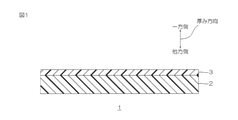
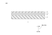
- FIG. 1 shows a cross-sectional view of a first embodiment of the laminated body of the present invention.
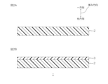
- 2A and 2B show an embodiment of the manufacturing method of the first embodiment of the laminate of the present invention,
- FIG. 2A shows a first step of preparing a base material, and
- FIG. 2B shows a base material.
- the second step of arranging the antifouling layer is shown.
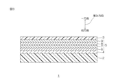
- FIG. 3 shows a cross-sectional view of a second embodiment of the laminated body of the present invention.
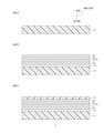
- 4A to 4C show one embodiment of the manufacturing method of the second embodiment of the laminate of the present invention,
- FIG. 4A shows a third step of preparing a base material, and
- FIG. 4B shows a base material.
- a fourth step of arranging the antireflection layer is shown, and FIG.
- FIG. 4C shows a fifth step of arranging the antifouling layer on the antireflection layer.
- FIG. 5 shows a cross-sectional view of a modified example of the first embodiment of the laminate of the present invention (a laminate having an adhesion layer between the base material and the antifouling layer).
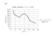
- FIG. 6 shows the result of in-plane diffraction (inplane) measurement and the result of fitting of Example 1.
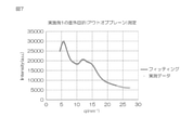
- FIG. 7 shows the result of the out-of-plane diffraction (out-of-plane) measurement of Example 1 and the result of fitting.
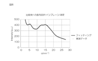
- FIG. 8 shows the result of in-plane diffraction (inplane) measurement and the result of fitting of Comparative Example 1.
- FIG. 1 shows a cross-sectional view of a modified example of the first embodiment of the laminate of the present invention (a laminate having an adhesion layer between the base material and the antifouling layer).
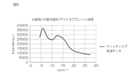
- FIG. 6 shows the result of in-plane diffraction (inplane) measurement and the result
- FIG. 9 shows the result of out-of-plane diffraction measurement and the result of fitting of Comparative Example 1.
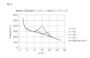
- FIG. 10 shows the fitting results (background curve and Gaussian curve) in the in-plane diffraction (inplane) measurement of Example 1.
- FIG. 11 shows the fitting results (background curve and Gaussian curve) in the out-of-plane diffraction measurement of Example 1.
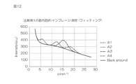
- FIG. 12 shows the fitting results (background curve and Gaussian curve) in the in-plane diffraction (inplane) measurement of Comparative Example 1.
- FIG. 13 shows the fitting results (background curve and Gaussian curve) in the out-of-plane diffraction measurement of Comparative Example 1.
- the vertical direction of the paper surface is the vertical direction (thickness direction)
- the upper side of the paper surface is the upper side (one side in the thickness direction)
- the lower side of the paper surface is the lower side (the other side in the thickness direction).
- the left-right direction and the depth direction of the paper surface are plane directions orthogonal to the vertical direction. Specifically, it conforms to the direction arrows in each figure.
- the laminated body 1 has a film shape (including a sheet shape) having a predetermined thickness, extends in a plane direction orthogonal to the thickness direction, and has a flat upper surface and a flat lower surface.
- the laminated body 1 includes a base material 2 and an antifouling layer 3 in order toward one side in the thickness direction. More specifically, the laminate 1 includes a base material 2 and an antifouling layer 3 directly arranged on the upper surface (one side in the thickness direction) of the base material 2.
- the thickness of the laminated body 1 is, for example, 300 ⁇ m or less, preferably 200 ⁇ m or less, and for example, 10 ⁇ m or more, preferably 30 ⁇ m or more.
- Base material The base material 2 is a treated body to which antifouling property is imparted by the antifouling layer 3.
- the base material 2 has a film shape.
- the base material 2 has flexibility.
- the base material 2 is arranged on the entire lower surface of the antifouling layer 3 so as to come into contact with the lower surface of the antifouling layer 3.
- Examples of the base material 2 include a polymer film.
- Examples of the material of the polymer film include polyester resins such as polyethylene terephthalate, polybutylene terephthalate, and polyethylene naphthalate, (meth) acrylic resins such as polymethacrylate, and olefin resins such as polyethylene, polypropylene, and cycloolefin polymers.
- Examples thereof include polycarbonate resin, polyether sulfone resin, polyarylate resin, melamine resin, polyamide resin, polyimide resin, for example, cellulose resin such as triacetyl cellulose, polystyrene resin and the like, preferably cellulose resin, more preferably. , Triacetyl cellulose and the like.
- the thickness of the base material 2 is, for example, 1 ⁇ m or more, preferably 5 ⁇ m or more, more preferably 10 ⁇ m or more, and for example, 200 ⁇ m or less, preferably 150 ⁇ m or less, more preferably 100 ⁇ m or less.
- the thickness of the base material 2 can be measured using a dial gauge ("DG-205" manufactured by PEACOCK).
- the base material 2 can be subjected to a surface treatment such as a hard coat treatment from the viewpoint of imparting scratch resistance, if necessary.
- the base material 2 can be imparted with antiglare property depending on the purpose and use.
- the antifouling layer 3 is a layer for preventing the adhesion of stains such as dirt and fingerprints to one side of the base material 2 in the thickness direction.
- the antifouling layer 3 has a thin film shape.
- the antifouling layer 3 is arranged on the entire upper surface of the base material 2 so as to be in contact with the upper surface of the base material 2.
- the antifouling layer 3 is formed of an alkoxysilane compound having a perfluoropolyether group.
- the antifouling layer 3 contains an alkoxysilane compound having a perfluoropolyether group, preferably an alkoxysilane compound having a perfluoropolyether group.
- Examples of the alkoxysilane compound having a perfluoropolyether group include compounds represented by the following general formula (1).
- R 1- R 2 -X- (CH 2 ) l- Si (OR 3 ) 3 (1)
- R 1 represents an alkyl fluoride group in which one or more hydrogen atoms are substituted with a fluorine atom
- R 2 is a structure containing at least one repeating structure of a perfluoropolyether group.
- R 3 indicates an alkyl group having 1 or more and 4 or less carbon atoms, and l indicates an integer of 1 or more.
- R 1 represents a linear or branched alkyl fluoride group (1 or more and 20 or less carbon atoms) in which one or more hydrogens are substituted with a fluorine atom, and preferably all hydrogen atoms of the alkyl group are used. The perfluoroalkyl group substituted with a fluorine atom is shown.
- R 2 is a repeating structure of the perfluoropolyether group represents at least one comprising structure preferably exhibits two containing structural repeating structure of the perfluoropolyether group.
- repeating structure of the perfluoropolyether group for example,-(OC n F 2n ) m- (m indicates an integer of 1 or more and 50 or less, and n indicates an integer of 1 or more and 20 or less.
- m indicates an integer of 1 or more and 50 or less
- n indicates an integer of 1 or more and 20 or less.
- Repeated structures of linear perfluoropolyether groups such as-(OC (CF 3 ) 2 ) m -,-(OCF 2 CF (CF 3 ) CF 2 ) m- and other branched perfluoros.
- Examples thereof include a repeating structure of a polyether group, preferably a repeating structure of a linear perfluoropolyether group, and more preferably- (OCF 2 ) m -,-(OC 2 F 4 ) m-. ..
- R 3 represents an alkyl group having 1 or more carbon atoms and 4 or less carbon atoms, and preferably a methyl group.
- X represents an ether group, a carbonyl group, an amino group, or an amide group, and preferably represents an ether group.
- L represents an integer of 1 or more, 20 or less, preferably 10 or less, and more preferably 5 or less. l more preferably indicates 3.
- alkoxysilane compounds having a perfluoropolyether group a compound represented by the following general formula (2) is preferable.
- P indicates an integer of 1 or more and 50 or less
- Q indicates an integer of 1 or more and 50 or less.
- the alkoxysilane compound having a perfluoropolyether group a commercially available product can also be used.
- Optool UD509 alkoxysilane compound having a perfluoropolyether group represented by the above general formula (2), Daikin Industries, Ltd.
- Optool UD120 manufactured by Daikin Industries, Ltd.
- the alkoxysilane compound having a perfluoropolyether group can be used alone or in combination of two or more.
- the antifouling layer 3 is formed by the method described later.
- the thickness of the antifouling layer 3 is, for example, 1 nm or more, preferably 5 nm or more, and for example, 30 nm or less, preferably 20 nm or less, more preferably 15 nm or less.
- the thickness of the antifouling layer 3 can be measured by fluorescent X-rays (ZXS PrimusII manufactured by Rigaku).
- Antifouling layer 3 in the plane diffraction at grazing incidence X-ray diffraction method (out-of-plane) measured has a peak at a wavenumber 2 nm -1 ⁇ 10 nm -1 attributed to lamellar structure. Further, the antifouling layer 3 has an integrated intensity ratio measured by a test described later of 0.0035 or less, preferably 0.0030 or less, more preferably 0.0020 or less, still more preferably 0.0010 or less. Is.
- Method for Manufacturing Laminated Body A method for manufacturing the laminated body 1 will be described with reference to FIGS. 2A and 2B.
- the manufacturing method of the method for manufacturing the laminated body 1 includes a first step of preparing the base material 2 and a second step of arranging the antifouling layer 3 on the base material 2. Further, in this manufacturing method, each layer is arranged in order by, for example, a roll-to-roll method.
- the base material 2 is prepared as shown in FIG. 2A.
- the antifouling layer 3 is arranged on the base material 2. Specifically, the antifouling layer 3 is arranged on one surface of the base material 2 in the thickness direction.
- the antifouling layer 3 On the base material 2, first, from the viewpoint of improving the adhesion between the base material 2 and the antifouling layer 3 on the surface of the base material 2, for example, corona treatment, plasma treatment, and frame treatment. , Ozone treatment, primer treatment, glow treatment, saponification treatment and other surface treatments.
- the surface of the base material 2 is subjected to plasma treatment.
- the adhesion of the antifouling layer 3 can be improved by appropriately adjusting the plasma treatment strength (W) and the type of gas. Further, it may be preferable to suppress the increase in surface unevenness of the base material 2 by not increasing the plasma processing intensity (W) too much from the viewpoint of adjusting the integrated intensity ratio described later to a predetermined range. be.
- Examples of the method for arranging the antifouling layer 3 on the base material 2 include a vacuum vapor deposition method and a wet coating method, and preferably, vacuum is used from the viewpoint of adjusting the integrated strength ratio described later to a predetermined range.
- a vapor deposition method can be mentioned.
- a vapor deposition source (alkoxysilane compound having a perfluoropolyether group) and a substrate 2 are placed facing each other in a vacuum chamber, and the vapor deposition source is heated to evaporate or sublimate, and the vapor deposition source is evaporated or sublimated. Is deposited on the surface of the substrate 2.
- the temperature of the vapor deposition source is, for example, 200 ° C. or higher, preferably 220 ° C. or higher, more preferably 240 ° C. or higher, from the viewpoint of adjusting the integrated intensity ratio described later to a predetermined range. Further, for example, the temperature is 330 ° C. or lower, preferably 300 ° C. or lower, and more preferably 280 ° C. or lower.
- the laminated body 1 is manufactured in which the antifouling layer 3 is arranged on one side of the base material 2 in the thickness direction, and the base material 2 and the antifouling layer 3 are sequentially provided on one side in the thickness direction.
- Operational effect antifouling layer 3 has in-plane diffraction at grazing incidence X-ray diffraction method (out-of-plane) measurement, at a wavenumber of 2 nm -1 ⁇ 10 nm -1 peak (peak attributed to a lamellar structure). Further, the antifouling layer 3 has an integrated intensity ratio measured by a test described later of 0.0035 or less, preferably 0.0030 or less, more preferably 0.0020 or less, still more preferably 0.0010 or less. Is.
- the integrated intensity (inplane diffraction integrated intensity) of the peak attributed to the lamellar structure is measured for the antifouling layer 3 by the in-plane diffraction (inplane) measurement in the micro-angle incident X-ray diffraction method. ..
- the integrated intensity (out-of-plane diffraction integrated intensity) of the peak attributed to the lamellar structure is measured by the out-of-plane diffraction (out-of-plane) measurement in the micro-angle incident X-ray diffraction method.
- the integrated intensity ratio of the in-plane diffraction integrated intensity to the out-of-plane diffraction integrated intensity is calculated. ..
- the out-of-plane diffraction integrated intensity is the integrated intensity of the diffraction peak due to the structure in which the lamella is oriented perpendicular to the substrate 2.
- the alkoxysilane compound having a perfluoropolyether group is also oriented perpendicular to the base material 2, so that the alkoxysilane located at the end thereof is oriented to the base material 2. It becomes easier to contact.
- the in-plane diffraction integrated intensity is the integrated intensity of the diffraction peak (peak at a wave number of 2 nm -1 to 10 nm -1 ) due to the structure in which the lamella is oriented parallel to the substrate 2.
- the alkoxysilane compound having a perfluoropolyether group is also oriented parallel to the base material 2, so that the alkoxysilane located at the end thereof is oriented parallel to the base material 2. It becomes difficult to contact.
- the structure in which the lamella is oriented perpendicularly to the base material 2 becomes relatively larger than the structure in which the lamella is oriented parallel to the base material 2.
- the ratio of the alkoxysilane located at the end of the alkoxysilane compound having a perfluoropolyether group in contact with the base material 2 increases.
- the integrated strength ratio is 0.0035 or less, the deterioration of the antifouling property of the antifouling layer 3 can be suppressed even after the dirt adhering to the antifouling layer 3 is wiped off (antifouling). Excellent durability.).
- the fact that the out-of-plane diffraction-integrated intensity is relatively larger than the in-plane diffraction-integrated intensity means that there are many lamellas stacked in the out-of-plane direction. When the lamellas are aligned in the out-of-plane direction, the fluorogroups at the ends are efficiently exposed on the surface, and excellent water repellency can be obtained.
- in-plane diffraction in-plane diffraction integral intensity
- out-of-plane diffraction out-of-plane diffraction integral intensity
- the plane diffraction at grazing incidence X-ray diffraction (in-plane) measurement peaks derived from periodic array of in-plane direction of the perfluoropolyether group (peak A4 (described later)) is wavenumber 1.5 ⁇ - Observed between 1 and 2.0 ⁇ -1.
- the same members and processes as those in the first embodiment are designated by the same reference numerals, and detailed description thereof will be omitted. Further, the second embodiment can exhibit the same effects as those of the first embodiment, except for special mention. Further, the first embodiment and the second embodiment can be combined as appropriate.
- the laminated body 1 includes a base material 2, a primer layer 4, an antireflection layer 5, and an antifouling layer 3 in order toward one side in the thickness direction. More specifically, the laminate 1 is directly placed on the base material 2, the primer layer 4 directly arranged on the upper surface (one side in the thickness direction) of the base material 2, and the upper surface (one side in the thickness direction) of the primer layer 4.
- the antireflection layer 5 to be arranged and the antifouling layer 3 directly arranged on the upper surface (one surface in the thickness direction) of the antireflection layer 5 are provided.
- the thickness of the laminated body 1 is, for example, 250 ⁇ m or less, preferably 200 ⁇ m or less, and for example, 10 ⁇ m or more, preferably 20 ⁇ m or more.
- the base material 2 is a base material for ensuring the mechanical strength of the laminated body 1.
- the base material 2 is arranged on the entire lower surface of the primer layer 4 so as to be in contact with the lower surface of the primer layer 4.
- Examples of the base material 2 include the same base material as the base material 2 in the first embodiment, preferably cellulose resin, polyester resin, and more preferably triacetyl cellulose and polyethylene terephthalate.
- the thickness of the base material 2 is the same as the thickness of the base material 2 in the first embodiment.
- Primer layer 4 is a layer for achieving adhesion between the base material 2 and the adhesion layer 11.
- the primer layer 4 is arranged on the entire lower surface of the antireflection layer 5 so as to be in contact with the lower surface of the antireflection layer 5.
- Preferred materials for the primer layer 4 include silicon oxide (SiO x ) (x is 1.2 or more and 1.9 or less) and indium tin oxide (ITO).
- the primer layer 4 is formed by the method described later.
- the anti-reflection layer 5 is a layer for suppressing reflection of external light.
- the antireflection layer 5 has a film shape.
- the antireflection layer 5 is arranged on the entire lower surface of the antifouling layer 3 so as to come into contact with the lower surface of the antifouling layer 3.
- the antireflection layer 5 is composed of two or more layers having different refractive indexes from each other.
- the antireflection layer 5 is composed of two or more layers having different refractive indexes from each other, the reflection of external light can be suppressed.
- the antireflection layer 5 is provided with a high refractive index layer having a relatively high refractive index and a low refractive index layer having a relatively low refractive index alternately toward one side in the thickness direction.
- the antireflection layer 5 (specifically, a high refractive index layer and a low refractive index layer) is a group consisting of a metal described later, an alloy described later, a metal oxide described later, a metal nitride described later, and a metal fluoride described later. It contains one selected from, preferably one selected from the group consisting of metals described below, metal oxides described below, and metal nitrides described below.
- the antireflection layer 5 has a first high refractive index layer 6, a first low refractive index layer 7, a second high refractive index layer 8, and a second low refractive index layer 9 in the thickness direction. A case of preparing in order toward the side will be described.
- Examples of the material of the low refractive index layer include a low refractive index material having a refractive index of 1.6 or less at a wavelength of 550 nm.
- the low refractive index material examples include silicon dioxide (SiO 2 ), magnesium fluoride and the like, and silicon dioxide is preferable. That is, preferably, the material of the first low refractive index layer 7 and the second low refractive index layer 9 is both silicon dioxide.
- silicon dioxide is selected as the material of the second low refractive index layer 9 from the viewpoint of adhesion to the antifouling layer 3.
- a layer containing silicon dioxide is selected as one surface of the antireflection layer 5 in the thickness direction (the surface in contact with the lower surface of the antifouling layer 3).
- the material of the second low refractive index layer 9 is silicon dioxide (preferably, the second low refractive index layer 9 is made of silicon dioxide), the antifouling durability can be further improved. can.
- Examples of the material of the high refractive index layer include a high refractive index material having a refractive index of 1.9 or more at a wavelength of 550 nm, and specific examples thereof. , Titanium oxide , niobide oxide (Nb 2 O 5 ), zirconium oxide, tin-doped indium oxide (ITO), antimony-doped tin oxide (ATO) and the like, and niobium oxide is preferable. That is, preferably, both the material of the first high refractive index layer 6 and the material of the second high refractive index layer 8 are niobium oxide.
- the thickness of the first high refractive index layer 6 is, for example, 1 nm or more, preferably 5 nm or more, and for example, 30 nm or less, preferably 20 nm or less.
- the thickness of the first low refractive index layer 7 is, for example, 10 nm or more, preferably 20 nm or more, and for example, 50 nm or less, preferably 30 nm or less.
- the ratio of the thickness of the first low refractive index layer 7 to the thickness of the first high refractive index layer 6 is, for example, 0.8 or more. It is preferably 1.0 or more, and is, for example, 10 or less, preferably 5 or less.
- the thickness of the second high refractive index layer 8 is, for example, 50 nm or more, preferably 80 nm or more, and for example, 200 nm or less, preferably 150 nm or less.
- the thickness of the second low refractive index layer 9 is, for example, 60 nm or more, preferably 80 nm or more, and for example, 150 nm or less, preferably 100 nm or less.
- the ratio of the thickness of the second low refractive index layer 9 to the thickness of the second high refractive index layer 8 is, for example, 0.5 or more. It is preferably 0.7 or more, and is, for example, 2.0 or less.
- the ratio of the thickness of the second high-refractive index layer 8 to the thickness of the first high-refractive index layer 6 is preferably 2 or more, for example. Is 7 or more, and is, for example, 15 or less, preferably 10 or less.
- the ratio of the thickness of the second low refractive index layer 9 to the thickness of the first low refractive index layer 7 is preferably 1 or more, for example. Is 3 or more, and is, for example, 10 or less, preferably 8 or less.
- the antireflection layer 5 is formed by a method described later.
- the thickness of the antireflection layer 5 is, for example, 100 nm or more, preferably 150 nm or more, and for example, 300 nm or less, preferably 250 nm or less.
- the thickness of the antireflection layer 5 can be measured by TEM observation of the cross section.
- the antifouling layer 3 has a thin film shape.
- the antifouling layer 3 is arranged on the entire upper surface of the antireflection layer 5 so as to be in contact with the upper surface of the antireflection layer 5.
- the antifouling layer 3 is formed of the above-mentioned alkoxysilane compound having a perfluoropolyether group (preferably, the above-mentioned alkoxysilane compound having a perfluoropolyether group represented by the general formula (2)).
- the antifouling layer 3 contains an alkoxysilane compound having a perfluoropolyether group, preferably an alkoxysilane compound having a perfluoropolyether group.
- the antifouling layer 3 is formed by the method described later.
- the thickness of the antifouling layer 3 is the same as the thickness of the antifouling layer 3 in the first embodiment.
- the manufacturing method of the method for manufacturing the laminated body 1 includes a third step of preparing the base material 2, a fourth step of arranging the primer layer 4 and the antireflection layer 5 on the base material 2, and an antireflection layer 5.
- a fifth step of arranging the dirty layer 3 is provided. Further, in this manufacturing method, each layer is arranged in order by, for example, a roll-to-roll method.
- the base material 2 is prepared as shown in FIG. 4A.
- the antireflection layer 5 is arranged on the base material 2. Specifically, the primer layer 4 and the antireflection layer 5 are arranged on one surface of the base material 2 in the thickness direction.
- the primer layer 4, the first high refractive index layer 6, the first low refractive index layer 7, the second high refractive index layer 8, and the second low refractive index layer 9 are placed on the base material 2. And are arranged in order toward one side in the thickness direction.
- the fourth step includes a primer layer arranging step of arranging the primer layer 4 on the base material 2 and a first high refractive index layer arranging step of arranging the first high refractive index layer 6 on the primer layer 4.
- the first low refractive index layer arranging step in which the first low refractive index layer 7 is arranged in the first high refractive index layer 6, and the second high in which the second high refractive index layer 8 is arranged in the first low refractive index layer 7. It includes a refractive index layer arranging step and a second low refractive index layer arranging step of arranging the second low refractive index layer 9 on the second high refractive index layer 8.
- each layer is arranged in order by, for example, a vacuum vapor deposition method, a sputtering method, a laminating method, a plating method, an ion plating method, preferably a sputtering method.
- the base material 2 for example, corona treatment, plasma treatment, frame treatment, ozone treatment, primer treatment, glow treatment, and saponification.
- Perform surface treatment such as plasma treatment.
- the surface of the base material 2 is subjected to plasma treatment.
- the targets (each layer (primer layer 4, the first high refractive index layer 6, the first low refractive index layer 7, the second high refractive index layer 8, and the second low refractive index layer) are placed in the vacuum chamber.
- the material with the index layer 9) and the base material 2 are arranged so as to face each other, gas is supplied and a voltage is applied from a power source to accelerate gas ions to irradiate the target, and the target material is ejected from the target surface.
- Each layer is sequentially deposited on the surface of the base material 2 with the target material.
- the gas examples include an inert gas such as Ar. Further, if necessary, a reactive gas such as oxygen gas can be used in combination.
- the flow rate ratio (sccm) of the reactive gas is not particularly limited, but for example, 0.1 flow rate% or more and 100 flow rate% or less with respect to the total flow rate ratio of the sputter gas and the reactive gas. Is.
- the atmospheric pressure during sputtering is, for example, 0.1 Pa or more, and is, for example, 1.0 Pa or less, preferably 0.7 Pa or less.
- the power supply may be, for example, any of a DC power supply, an AC power supply, an MF power supply, and an RF power supply, or may be a combination thereof.
- the primer layer 4 and the antireflection layer 5 are arranged on one surface of the base material 2 in the thickness direction.
- the antifouling layer 3 is arranged on the antireflection layer 5. Specifically, the antifouling layer 3 is arranged on one side of the antireflection layer 5 in the thickness direction.
- Examples of the method for arranging the antifouling layer 3 on the antireflection layer 5 include a vacuum vapor deposition method, a wet coating method, and the like. The law is mentioned.
- a vapor deposition source alkoxysilane compound having a perfluoropolyether group
- an antireflection layer 5 are placed facing each other in a vacuum chamber, and the vapor deposition source is heated to evaporate or sublimate to evaporate or sublimate the vapor deposition.
- the source is deposited on the surface of the antireflection layer 5.
- the temperature of the vapor deposition source is, for example, 200 ° C. or higher, preferably 220 ° C. or higher, more preferably 240 ° C. or higher, and for example, 330 ° C. or lower, preferably 300 ° C. or lower. More preferably, it is 280 ° C. or lower.
- the antifouling layer 3 is arranged on one side of the antireflection layer 5 in the thickness direction, and the base material 2, the antireflection layer 5, and the antifouling layer 3 are sequentially provided on one side in the thickness direction. Is manufactured.
- the laminated body 1 includes an antireflection layer 5 between the base material 2 and the antifouling layer 3. Therefore, it is possible to suppress the reflection of external light.
- a second layer containing silicon dioxide (for example, a second layer made of silicon dioxide) is formed on the lower surface of the antifouling layer 3.
- the hydrolyzing group (-(OR 3 ) in the above formula (1)) in the alkoxysilane compound having the perfluoropolyether group of the antifouling layer 3 is hydrated.
- the silanol group generated in the process of decomposition and silicon in silicon dioxide undergo a dehydration condensation reaction.
- an alkoxysilane compound having a perfluoropolyether group is formed on the antireflection layer 5 via a siloxane bond. This makes it possible to further improve the antifouling durability.
- the laminate 1 includes the base material 2 and the antifouling layer 3, but as shown in FIG. 5, between the base material 2 and the antifouling layer 3, the primer layer 4 and the antifouling layer 3 are further provided.
- the adhesion layer 11 can also be provided.
- the adhesion layer 11 may be provided between the base material 2 and the antifouling layer 3, and the primer layer 4 may be provided between the base material 2 and the adhesion layer 11.
- the laminated body 1 is provided with the base material 2, the primer layer 4, the adhesion layer 11, and the antifouling layer 3 in order toward one side in the thickness direction.
- the adhesion layer 11 is a layer that adheres to the antifouling layer 3.
- the material of the adhesion layer 11 is preferably silicon dioxide (SiO 2 ). In other words, preferably, the material of the adhesion layer 11 contains at least silicon dioxide (SiO 2 ). More preferably, the adhesion layer 11 is made of silicon dioxide (SiO 2 ).
- the material of the adhesion layer 11 is silicon dioxide (SiO 2 )
- the hydrolyzing group (-(OR 3 ) in the above formula (1)) in the alkoxysilane compound having a perfluoropolyether group of the antifouling layer 3 The silanol group generated in the process of hydrolysis and silicon in silicon dioxide undergo a dehydration condensation reaction.
- an alkoxysilane compound having a perfluoropolyether group is formed in the adhesion layer 11 via a siloxane bond. This makes it possible to further improve the antifouling durability.
- the adhesion layer 11 is formed by, for example, a sputtering method, a plasma CVD method, a vacuum vapor deposition method, or the like.
- the antireflection layer 5 includes two high refractive index layers having a relatively high refractive index and two low refractive index layers having a relatively low refractive index, but has a high refractive index.
- the number of layers and the low refractive index layer is not particularly limited.
- TAC film (thickness 80 ⁇ m) was prepared as a base material.
- a hard coat layer was placed on one side of the base material (TAC film) in the thickness direction.
- an ultraviolet curable acrylic resin composition manufactured by DIC, trade name "GRANDIC PC-1070", refractive index at a wavelength of 405 nm: 1.55
- the amount of silica particles per 100 parts by mass of the resin component is 25.
- Organo silica sol (“MEK-ST-L” manufactured by Nissan Chemical Co., Ltd., average primary particle size of silica particles (inorganic filler): 50 nm, particle size distribution of silica particles: 30 nm to 130 nm, solid content 30 so as to be parts by mass. Mass%) was added and mixed to prepare a hard coat composition.
- the hardcourt composition was applied to one side of the triacetyl cellulose (TAC) in the thickness direction so that the thickness after drying was 6 ⁇ m, and dried at 80 ° C. for 3 minutes. Then, using a high-pressure mercury lamp , ultraviolet rays having an integrated light intensity of 200 mJ / cm 2 were irradiated to cure the coating layer and form a hard coat layer.
- TAC triacetyl cellulose
- the triacetyl cellulose film on which the hard coat layer was formed was introduced into a roll-to-toll type sputter film forming apparatus, and the hard coat layer forming surface was bombarded (plasma treatment with Ar gas, 100 W) while the film was running. ), Then, by the sputtering method, an ITO layer (primer layer) having a thickness of 3.5 nm and an Nb 2 O 5 layer (first high refractive index layer) having a thickness of 12 nm are placed on one surface of the substrate (hard coat layer) in the thickness direction.
- ITO layer primary layer
- Nb 2 O 5 layer first high refractive index layer
- a SiO 2 layer (first low refractive index layer) having a thickness of 28 nm, an Nb 2 O 5 layer (second high refractive index layer) having a thickness of 100 nm, and a SiO 2 (second low refractive index layer) having a thickness of 85 nm were arranged in this order. ..
- the primer layer, the first high refractive index layer, the first low refractive index layer, the second high refractive index layer, and the second low refractive index layer are placed on one side in the thickness direction of the base material in the thickness direction. Anti-reflection layers are arranged in order toward the side.
- one surface of the antireflection layer in the thickness direction was subjected to plasma treatment (100 W) with oxygen gas, and then Optool UD509 (an alkoxysilane compound having a perfluoropolyether group represented by the above general formula (2), manufactured by Daikin Industries, Ltd.). ) was used as the vapor deposition source, and an antifouling layer having a thickness of 7 nm was arranged on one side of the antireflection layer in the thickness direction.
- Optool UD509 an alkoxysilane compound having a perfluoropolyether group represented by the above general formula (2), manufactured by Daikin Industries, Ltd.
- the temperature of the vapor deposition source (crucible) was 260 ° C.
- Comparative Example 1 Optool UD509 is applied to one side of the antireflection layer in the thickness direction with a gravure coater so that the coating thickness is 8 ⁇ m, and then heat-treated at a drying temperature of 60 ° C. for 60 seconds to obtain one in the thickness direction of the antireflection layer.
- a laminated body was produced by the same procedure as in Example 1 except that an antifouling layer having a thickness of 7 nm was arranged in the direction.
- Example 2 A laminated body was manufactured by the same procedure as in Example 1.
- the step of forming the antifouling layer after plasma treatment (100 W) with argon gas on one side of the antireflection layer in the thickness direction, a vacuum vapor deposition method using Optool UD120 (manufactured by Daikin Industries, Ltd.) as a vapor deposition source is used.
- An antifouling layer having a thickness of 7 nm was arranged on one surface of the antireflection layer in the thickness direction.
- Comparative Example 2 A laminated body was manufactured by the same procedure as in Example 1. However, in the vacuum vapor deposition method, the temperature of the vapor deposition source (crucible) was changed to 190 ° C.
- Comparative Example 3 A laminated body was manufactured by the same procedure as in Example 1.
- the step of forming the antifouling layer after plasma treatment (4500 W) with argon gas on one side of the antireflection layer in the thickness direction, a vacuum vapor deposition method using Optool UD120 (manufactured by Daikin Industries, Ltd.) as a vapor deposition source is used.
- An antifouling layer having a thickness of 7 nm was arranged on one surface of the antireflection layer in the thickness direction.
- in-plane diffraction (in-plane) measurement and out-of-plane diffraction (out of plane) are performed by the micro-angle incident X-ray diffraction method based on the following conditions. Measurements were performed.
- Example 1 The result of the in-plane diffraction (in-plane) measurement of Example 1 is shown in FIG. 6, the result of the out-of-plane diffraction (out-of-plane) measurement of Example 1 is shown in FIG. 7, and the in-plane diffraction of Comparative Example 1 is shown.
- the result of the (in-plane) measurement is shown in FIG. 8, and the result of the out-of-plane diffraction (out-of-plane) measurement of Comparative Example 1 is shown in FIG.
- Peak intensity (n is an integer of 1 to 4)
- a 1 indicates the peak intensity of peak A1
- a 2 indicates the peak intensity of peak A2
- a 3 indicates the peak intensity of peak A3.
- a 4 represents a.) indicating the peak intensity of the peak A4, q an center-of-gravity position (q A1 indicates the position of the center of gravity of the peak A1, q A2 indicates the position of the center of gravity of the peak A2, q A3 Indicates the position of the center of gravity of the peak A3, q A4 indicates the position of the center of gravity of the peak A4), ⁇ q An indicates the half-value full width ( ⁇ q A1 indicates the half-value full width of the peak A1, and ⁇ q A2 indicates the peak. The half-price full width of A2 is shown, ⁇ q A3 shows the half-price full width of the peak A3, and ⁇ q A4 shows the half-price full width of the peak A4).
- the measured data in-plane diffraction (inplane) measurement
- the measured data can be shown as the sum of the background and the peaks A1 to A4.
- Inplane diffraction integrated intensity peak intensity (A 1 ) x full width at half maximum ( ⁇ q A1 ) (4)
- N is an integer of 1 to 3
- B 1 indicates the peak intensity of peak B 1
- B 2 indicates the peak intensity of peak B 2
- B 3 indicates the peak intensity of peak B 3.
- q Bn indicates the position of the center of gravity
- q B1 indicates the position of the center of gravity of the peak B1
- q B2 indicates the position of the center of gravity of the peak B2
- q B3 indicates the position of the center of gravity of the peak B3.
- Bn indicates the half-value full width ( ⁇ q B1 indicates the half-value full width of the peak B1, ⁇ q B2 indicates the half-value full width of the peak B2, and ⁇ q B3 indicates the half-value full width of the peak B3).
- the measured data (out-of-plane diffraction (out-of-plane) measurement) can be shown as the sum of the background and the peaks B1 to B3.
- Amount of change in contact angle initial contact angle-contact angle after eraser sliding test (7)
- the laminate of the present invention is suitably used, for example, in an antireflection film with an antifouling layer, a transparent conductive film with an antifouling layer, and an electromagnetic wave shielding film with an antifouling layer.
Landscapes
- Chemical & Material Sciences (AREA)
- Chemical Kinetics & Catalysis (AREA)
- Physics & Mathematics (AREA)
- Organic Chemistry (AREA)
- Mechanical Engineering (AREA)
- Metallurgy (AREA)
- Materials Engineering (AREA)
- Engineering & Computer Science (AREA)
- General Physics & Mathematics (AREA)
- Optics & Photonics (AREA)
- Inorganic Chemistry (AREA)
- Laminated Bodies (AREA)
- Surface Treatment Of Optical Elements (AREA)
- Paints Or Removers (AREA)
Abstract
Description
前記防汚層が、パーフルオロポリエーテル基を有するアルコキシシラン化合物を含み、微小角入射X線回折法における面外回折(アウトオブプレーン)測定において、ラメラ構造に帰属される波数2nm-1~10nm-1にピークを有し、下記試験により測定される前記防汚層の積分強度比が、0.0035以下である、積層体である。
試験:防汚層について、微小角入射X線回折法における面内回折(インプレーン)測定により、ラメラ構造に帰属されるピークの積分強度(インプレーン回折積分強度)を測定する。別途、防汚層について、微小角入射X線回折法における面外回折(アウトオブプレーン)測定により、ラメラ構造に帰属されるピークの積分強度(アウトオブプレーン回折積分強度)を測定する。得られたインプレーン回折積分強度およびアウトオブプレーン回折積分強度に基づき、アウトオブプレーン回折積分強度に対するインプレーン回折積分強度の積分強度比(インプレーン回折積分強度/アウトオブプレーン回折積分強度)を算出する。
図1を参照して、本発明の積層体の第1実施形態を説明する。
積層体1は、所定の厚みを有するフィルム形状(シート形状を含む)を有し、厚み方向と直交する面方向に延び、平坦な上面および平坦な下面を有する。
基材2は、防汚層3によって、防汚性を付与される被処理体である。
防汚層3は、基材2の厚み方向一方側に対して、垢、指紋などの汚れの付着を防止するための層である。
R1-R2-X-(CH2)l-Si(OR3)3 (1)
(上記式(1)において、R1は、1つ以上の水素原子がフッ素原子によって置換されたフッ化アルキル基を示し、R2は、パーフルオロポリエーテル基の繰り返し構造を少なくとも1つ含む構造を示し、R3は、炭素数1以上4以下アルキル基を示し、lは、1以上の整数を示す。)
R1は、1つ以上の水素がフッ素原子によって置換された、直鎖状又は分岐状のフッ化アルキル基(炭素数1以上20以下)を示し、好ましくは、アルキル基の水素原子のすべてをフッ素原子に置換したパーフルオロアルキル基を示す。
CF3-(OCF2)P-(OC2F4)Q-O-(CH2)3-Si(OCH3)3 (2)
(上記式(2)において、Pは、1以上50以下の整数を示し、Qは、1以上50以下の整数を示す。)
パーフルオロポリエーテル基を有するアルコキシシラン化合物は、市販品を用いることもでき、具体的には、オプツールUD509(上記一般式(2)で示されるパーフルオロポリエーテル基を有するアルコキシシラン化合物、ダイキン工業社製)、オプツールUD120(ダイキン工業株式会社製)などが挙げられる。
図2Aおよび図2Bを参照して、積層体1の製造方法を説明する。
防汚層3は、微小角入射X線回折法における面外回折(アウトオブプレーン)測定において、波数2nm-1~10nm-1にピーク(ラメラ構造に帰属されるピーク)を有する。また、防汚層3は、後述する試験により測定される積分強度比が、0.0035以下、好ましくは、0.0030以下、より好ましくは、0.0020以下、さらに好ましくは、0.0010以下である。
図3を参照して、本発明の積層体の第2実施形態を説明する。
図3に示すように、積層体1は、基材2と、プライマー層4と、反射防止層5と、防汚層3とを厚み方向一方側に向かって順に備える。積層体1は、より具体的には、基材2と、基材2の上面(厚み方向一方面)に直接配置されるプライマー層4と、プライマー層4の上面(厚み方向一方面)に直接配置される反射防止層5と、反射防止層5の上面(厚み方向一方面)に直接配置される防汚層3とを備える。
基材2は、積層体1の機械強度を確保するための基材である。
プライマー層4は、基材2と密着層11との密着を図るための層である。
反射防止層5は、外光の反射を抑制するための層である。
防汚層3は、薄膜形状を有する。防汚層3は、反射防止層5の上面全面に、反射防止層5の上面に接触するように、配置されている。
図4A~図4Cを参照して、積層体1の製造方法を説明する。
積層体1は、基材2および防汚層3の間に、反射防止層5を備える。そのため、外光の反射を抑制することができる。
変形例において、第1実施形態および第2実施形態と同様の部材および工程については、同一の参照符号を付し、その詳細な説明を省略する。また、変形例は、特記する以外、第1実施形態および第2実施形態と同様の作用効果を奏することができる。さらに、第1実施形態、第2実施形態およびその変形例を適宜組み合わせることができる。
実施例1
基材として、トリアセチルセルロース(TAC)フィルム(厚さ80μm)を準備した。基材(TACフィルム)の厚み方向一方面に、ハードコート層を配置した。具体的には、紫外線硬化性アクリル系樹脂組成物(DIC製、商品名「GRANDIC PC-1070」、波長405nmにおける屈折率:1.55)に、樹脂成分100質量部に対するシリカ粒子の量が25質量部となるように、オルガノシリカゾル(日産化学社製「MEK-ST-L」、シリカ粒子(無機フィラー)の平均一次粒子径:50nm、シリカ粒子の粒子径分布:30nm~130nm、固形分30質量%)を添加して混合し、ハードコート組成物を調製した。トリアセチルセルロース(TAC)の厚み方向一方面に、ハードコート組成物を、乾燥後の厚みが6μmとなるように塗布し、80℃で3分間乾燥した。その後、高圧水銀ランプを用いて、積算光量200mJ/cm2の紫外線を照射し、塗布層を硬化させハードコート層を形成した。
反射防止層の厚み方向一方面に、オプツールUD509を、グラビアコーターで塗工厚み8μmになるように塗工した後、乾燥温度60℃で60秒加熱処理することにより、反射防止層の厚み方向一方面に厚み7nmの防汚層を配置した以外は、実施例1と同様の手順で、積層体を製造した。
実施例1と同様の手順で、積層体を製造した。
実施例1と同様の手順で、積層体を製造した。
但し、真空蒸着法において、蒸着源(るつぼ)の温度を190℃に変更した。
実施例1と同様の手順で、積層体を製造した。
(微小角入射X線回折測定)
各実施例および各比較例の積層体の防汚層について、以下の条件に基づき、微小角入射X線回折法により、面内回折(インプレーン)測定、および、面外回折(アウトオブプレーン)測定を実施した。
実験施設:あいちシンクロトロン光センター
実験ステーション:BL8S1
入射エネルギー:14.4keV
ビームサイズ:500μm(横幅)×40μm(縦)
試料角:入射光に対して0.1度
検出器:2次元検出器 PILATAS
試料設置方法:薄く塗布したグリスにて平面試料台上に固定
以下、得られた面内回折(インプレーン)測定および面外回折(アウトオブプレーン)測定の結果から、アウトオブプレーン回折積分強度およびインプレーン回折積分強度を算出した。算出方法は、アウトオブプレーン回折積分強度およびインプレーン回折積分強度を画一的に算出する観点から、フィッティング法を用いた。その方法について、詳述する。


各実施例および各比較例の積層体の防汚層について、協和界面科学社製DMo-501を用いて、以下の条件に基づき、防汚層の純水に対する接触角(初期接触角と称する場合がある。)を測定した。その結果を表1に示す。
液滴量:2μl
温度:25℃
湿度:40%
次いで、各実施例および各比較例の積層体の防汚層について、以下の条件に基づき、消しゴム摺動試験を実施した後、上記した方法と同様の手順で、水接触角(消しゴム摺動試験後の接触角と称する場合がある。)を測定した。その結果を表1に示す。
Minoan社製の消しゴム(Φ6mm)
摺動距離:片道100mm
摺動速度:100mm/秒
荷重:1kg/6mmΦ
回数:3000回
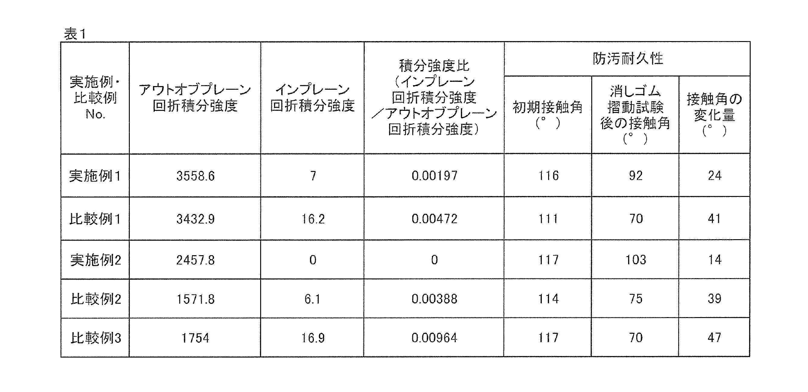
積分強度比が、0.0035以下である実施例1~実施例2の水接触角の変化量は、積分強度比が0.0035を超過する比較例1~比較例3の水接触角の変化量に比べて小さい。このことから、積分強度比が0.0035以下であれば、防汚層に付着した汚れを拭き取った後でも、防汚層の防汚性の低下を抑制できるとわかる。
2 基材
3 防汚層
4 プライマー層
5 反射防止層
Claims (10)
- 基材と、防汚層とを厚み方向一方側に向かって順に備え、
前記防汚層が、パーフルオロポリエーテル基を有するアルコキシシラン化合物を含み、
微小角入射X線回折法における面外回折(アウトオブプレーン)測定において、ラメラ構造に帰属される波数2nm-1~10nm-1にピークを有し、
下記試験により測定される前記防汚層の積分強度比が、0.0035以下であることを特徴とする、積層体。
試験:防汚層について、微小角入射X線回折法における面内回折(インプレーン)測定により、ラメラ構造に帰属されるピークの積分強度(インプレーン回折積分強度)を測定する。別途、防汚層について、微小角入射X線回折法における面外回折(アウトオブプレーン)測定により、ラメラ構造に帰属されるピークの積分強度(アウトオブプレーン回折積分強度)を測定する。得られたインプレーン回折積分強度およびアウトオブプレーン回折積分強度に基づき、アウトオブプレーン回折積分強度に対するインプレーン回折積分強度の積分強度比(インプレーン回折積分強度/アウトオブプレーン回折積分強度)を算出する。 - 前記基材および前記防汚層の間に、さらに、密着層を備えることを特徴とする、請求項1に記載の積層体。
- 前記密着層は、二酸化ケイ素を含む層であることを特徴とする、請求項2に記載の積層体。
- 前記防汚層は、パーフルオロポリエーテル基を有するアルコキシシラン化合物が、シロキサン結合を介して、前記密着層に形成されていることを特徴とする、請求項3に記載の積層体。
- 前記基材と前記密着層との間に、さらに、プライマー層を備えることを特徴とする、請求項3または4に記載の積層体。
- 前記基材および前記防汚層の間に、さらに、反射防止層を備えることを特徴とする、請求項1または2に記載の積層体。
- 前記反射防止層は、互いに異なる屈折率を有する2以上の層からなることを特徴とする、請求項6に記載の積層体。
- 前記反射防止層は、金属、金属酸化物、金属窒化物からなる群から選択される1種を含むことを特徴とする、請求項7に記載の積層体。
- 前記反射防止層の厚み方向一方面は、二酸化ケイ素を含む層であることを特徴とする、請求項7または請求項8に記載の積層体。
- 前記基材および前記反射防止層の間に、さらに、プライマー層を備えることを特徴とする、請求項6~9のいずれか一つに記載の積層体。
Priority Applications (3)
| Application Number | Priority Date | Filing Date | Title |
|---|---|---|---|
| CN202180061138.0A CN116234692B (zh) | 2020-07-13 | 2021-07-13 | 层叠体 |
| KR1020227045523A KR102518575B1 (ko) | 2020-07-13 | 2021-07-13 | 적층체 |
| JP2022536370A JP7185100B2 (ja) | 2020-07-13 | 2021-07-13 | 積層体 |
Applications Claiming Priority (2)
| Application Number | Priority Date | Filing Date | Title |
|---|---|---|---|
| JP2020120131 | 2020-07-13 | ||
| JP2020-120131 | 2020-07-13 |
Publications (1)
| Publication Number | Publication Date |
|---|---|
| WO2022014566A1 true WO2022014566A1 (ja) | 2022-01-20 |
Family
ID=79555554
Family Applications (1)
| Application Number | Title | Priority Date | Filing Date |
|---|---|---|---|
| PCT/JP2021/026244 Ceased WO2022014566A1 (ja) | 2020-07-13 | 2021-07-13 | 積層体 |
Country Status (5)
| Country | Link |
|---|---|
| JP (1) | JP7185100B2 (ja) |
| KR (1) | KR102518575B1 (ja) |
| CN (1) | CN116234692B (ja) |
| TW (2) | TW202346090A (ja) |
| WO (1) | WO2022014566A1 (ja) |
Cited By (1)
| Publication number | Priority date | Publication date | Assignee | Title |
|---|---|---|---|---|
| CN117721424A (zh) * | 2023-12-21 | 2024-03-19 | 深圳市派恩新材料技术有限公司 | 含氟靶材、功能膜层及其真空溅射成型方法 |
Families Citing this family (1)
| Publication number | Priority date | Publication date | Assignee | Title |
|---|---|---|---|---|
| CN119191726A (zh) * | 2023-06-14 | 2024-12-27 | 大金工业株式会社 | 基材处理方法 |
Citations (8)
| Publication number | Priority date | Publication date | Assignee | Title |
|---|---|---|---|---|
| JP2005007320A (ja) * | 2003-06-19 | 2005-01-13 | Mitsui Chemicals Inc | 複合多層膜、その自己組織的な製造方法および電子部品 |
| JP2005301208A (ja) * | 2004-03-17 | 2005-10-27 | Seiko Epson Corp | 防汚性光学物品の製造方法 |
| US20070104891A1 (en) * | 2005-11-04 | 2007-05-10 | Essilor International Compagnie Generale D'optique | Process for coating an optical article with an anti-fouling surface coating by vacuum evaporation |
| JP2009139530A (ja) * | 2007-12-05 | 2009-06-25 | Seiko Epson Corp | 光学物品の製造方法 |
| JP2009251008A (ja) * | 2008-04-01 | 2009-10-29 | Seiko Epson Corp | 光学物品およびその製造方法 |
| JP2010076422A (ja) * | 2008-08-27 | 2010-04-08 | Ricoh Co Ltd | 液体吐出ヘッド及び画像形成装置並びに液体吐出ヘッドの製造方法 |
| JP2011021091A (ja) * | 2009-07-15 | 2011-02-03 | T & K:Kk | 樹脂表面改質方法および表面改質樹脂基材 |
| JP2018004921A (ja) * | 2016-06-30 | 2018-01-11 | ホヤ レンズ タイランド リミテッドHOYA Lens Thailand Ltd | 眼鏡レンズ及び眼鏡レンズの製造方法 |
Family Cites Families (4)
| Publication number | Priority date | Publication date | Assignee | Title |
|---|---|---|---|---|
| JPH1171665A (ja) | 1997-08-29 | 1999-03-16 | Toppan Printing Co Ltd | 防汚性薄膜の形成方法 |
| JP2006124417A (ja) * | 2004-10-26 | 2006-05-18 | Asahi Glass Co Ltd | 防汚層形成用組成物および反射防止積層体 |
| JP4589186B2 (ja) * | 2005-07-04 | 2010-12-01 | ディバーシー株式会社 | 清掃装置およびそれを取り付けた床洗浄機ならびにその床洗浄機を用いた床面管理作業方法 |
| JP6477815B2 (ja) * | 2016-09-23 | 2019-03-06 | ダイキン工業株式会社 | 撥水性を有する基材 |
-
2021
- 2021-07-13 CN CN202180061138.0A patent/CN116234692B/zh active Active
- 2021-07-13 JP JP2022536370A patent/JP7185100B2/ja active Active
- 2021-07-13 TW TW112128830A patent/TW202346090A/zh unknown
- 2021-07-13 WO PCT/JP2021/026244 patent/WO2022014566A1/ja not_active Ceased
- 2021-07-13 KR KR1020227045523A patent/KR102518575B1/ko active Active
- 2021-07-13 TW TW110125738A patent/TWI864309B/zh active
Patent Citations (8)
| Publication number | Priority date | Publication date | Assignee | Title |
|---|---|---|---|---|
| JP2005007320A (ja) * | 2003-06-19 | 2005-01-13 | Mitsui Chemicals Inc | 複合多層膜、その自己組織的な製造方法および電子部品 |
| JP2005301208A (ja) * | 2004-03-17 | 2005-10-27 | Seiko Epson Corp | 防汚性光学物品の製造方法 |
| US20070104891A1 (en) * | 2005-11-04 | 2007-05-10 | Essilor International Compagnie Generale D'optique | Process for coating an optical article with an anti-fouling surface coating by vacuum evaporation |
| JP2009139530A (ja) * | 2007-12-05 | 2009-06-25 | Seiko Epson Corp | 光学物品の製造方法 |
| JP2009251008A (ja) * | 2008-04-01 | 2009-10-29 | Seiko Epson Corp | 光学物品およびその製造方法 |
| JP2010076422A (ja) * | 2008-08-27 | 2010-04-08 | Ricoh Co Ltd | 液体吐出ヘッド及び画像形成装置並びに液体吐出ヘッドの製造方法 |
| JP2011021091A (ja) * | 2009-07-15 | 2011-02-03 | T & K:Kk | 樹脂表面改質方法および表面改質樹脂基材 |
| JP2018004921A (ja) * | 2016-06-30 | 2018-01-11 | ホヤ レンズ タイランド リミテッドHOYA Lens Thailand Ltd | 眼鏡レンズ及び眼鏡レンズの製造方法 |
Cited By (1)
| Publication number | Priority date | Publication date | Assignee | Title |
|---|---|---|---|---|
| CN117721424A (zh) * | 2023-12-21 | 2024-03-19 | 深圳市派恩新材料技术有限公司 | 含氟靶材、功能膜层及其真空溅射成型方法 |
Also Published As
| Publication number | Publication date |
|---|---|
| JP7185100B2 (ja) | 2022-12-06 |
| TWI864309B (zh) | 2024-12-01 |
| KR102518575B1 (ko) | 2023-04-05 |
| KR20230009993A (ko) | 2023-01-17 |
| TW202346090A (zh) | 2023-12-01 |
| CN116234692B (zh) | 2024-03-19 |
| CN116234692A (zh) | 2023-06-06 |
| JPWO2022014566A1 (ja) | 2022-01-20 |
| TW202206287A (zh) | 2022-02-16 |
Similar Documents
| Publication | Publication Date | Title |
|---|---|---|
| TWI817160B (zh) | 附防汙層之光學膜 | |
| TWI811736B (zh) | 附防汙層之光學膜 | |
| JP7185100B2 (ja) | 積層体 | |
| TWI811735B (zh) | 附防污層之光學膜 | |
| JP7186333B2 (ja) | 積層体 | |
| JP7186332B2 (ja) | 積層体 | |
| JP7186334B2 (ja) | 積層体 | |
| WO2022014574A1 (ja) | 積層体 | |
| WO2024116961A1 (ja) | 光学物品の製造方法 |
Legal Events
| Date | Code | Title | Description |
|---|---|---|---|
| 121 | Ep: the epo has been informed by wipo that ep was designated in this application |
Ref document number: 21842858 Country of ref document: EP Kind code of ref document: A1 |
|
| ENP | Entry into the national phase |
Ref document number: 2022536370 Country of ref document: JP Kind code of ref document: A |
|
| ENP | Entry into the national phase |
Ref document number: 20227045523 Country of ref document: KR Kind code of ref document: A |
|
| NENP | Non-entry into the national phase |
Ref country code: DE |
|
| 122 | Ep: pct application non-entry in european phase |
Ref document number: 21842858 Country of ref document: EP Kind code of ref document: A1 |