WO2022014283A1 - 半導体装置及びモータ駆動システム - Google Patents
半導体装置及びモータ駆動システム Download PDFInfo
- Publication number
- WO2022014283A1 WO2022014283A1 PCT/JP2021/023767 JP2021023767W WO2022014283A1 WO 2022014283 A1 WO2022014283 A1 WO 2022014283A1 JP 2021023767 W JP2021023767 W JP 2021023767W WO 2022014283 A1 WO2022014283 A1 WO 2022014283A1
- Authority
- WO
- WIPO (PCT)
- Prior art keywords
- leads
- semiconductor device
- lead
- sense
- short
- Prior art date
- Legal status (The legal status is an assumption and is not a legal conclusion. Google has not performed a legal analysis and makes no representation as to the accuracy of the status listed.)
- Ceased
Links
Images










Classifications
-
- H—ELECTRICITY
- H02—GENERATION; CONVERSION OR DISTRIBUTION OF ELECTRIC POWER
- H02K—DYNAMO-ELECTRIC MACHINES
- H02K11/00—Structural association of dynamo-electric machines with electric components or with devices for shielding, monitoring or protection
- H02K11/20—Structural association of dynamo-electric machines with electric components or with devices for shielding, monitoring or protection for measuring, monitoring, testing, protecting or switching
- H02K11/27—Devices for sensing current, or actuated thereby
-
- G—PHYSICS
- G01—MEASURING; TESTING
- G01R—MEASURING ELECTRIC VARIABLES; MEASURING MAGNETIC VARIABLES
- G01R1/00—Details of instruments or arrangements of the types included in groups G01R5/00 - G01R13/00 and G01R31/00
- G01R1/20—Modifications of basic electric elements for use in electric measuring instruments; Structural combinations of such elements with such instruments
- G01R1/203—Resistors used for electric measuring, e.g. decade resistors standards, resistors for comparators, series resistors, shunts
-
- G—PHYSICS
- G01—MEASURING; TESTING
- G01R—MEASURING ELECTRIC VARIABLES; MEASURING MAGNETIC VARIABLES
- G01R19/00—Arrangements for measuring currents or voltages or for indicating presence or sign thereof
- G01R19/0092—Measuring current only
-
- H—ELECTRICITY
- H02—GENERATION; CONVERSION OR DISTRIBUTION OF ELECTRIC POWER
- H02P—CONTROL OR REGULATION OF ELECTRIC MOTORS, ELECTRIC GENERATORS OR DYNAMO-ELECTRIC CONVERTERS; CONTROLLING TRANSFORMERS, REACTORS OR CHOKE COILS
- H02P21/00—Arrangements or methods for the control of electric machines by vector control, e.g. by control of field orientation
- H02P21/22—Current control, e.g. using a current control loop
-
- H—ELECTRICITY
- H02—GENERATION; CONVERSION OR DISTRIBUTION OF ELECTRIC POWER
- H02P—CONTROL OR REGULATION OF ELECTRIC MOTORS, ELECTRIC GENERATORS OR DYNAMO-ELECTRIC CONVERTERS; CONTROLLING TRANSFORMERS, REACTORS OR CHOKE COILS
- H02P27/00—Arrangements or methods for the control of AC motors characterised by the kind of supply voltage
- H02P27/04—Arrangements or methods for the control of AC motors characterised by the kind of supply voltage using variable-frequency supply voltage, e.g. inverter or converter supply voltage
- H02P27/06—Arrangements or methods for the control of AC motors characterised by the kind of supply voltage using variable-frequency supply voltage, e.g. inverter or converter supply voltage using DC to AC converters or inverters
-
- H—ELECTRICITY
- H10—SEMICONDUCTOR DEVICES; ELECTRIC SOLID-STATE DEVICES NOT OTHERWISE PROVIDED FOR
- H10W—GENERIC PACKAGES, INTERCONNECTIONS, CONNECTORS OR OTHER CONSTRUCTIONAL DETAILS OF DEVICES COVERED BY CLASS H10
- H10W70/00—Package substrates; Interposers; Redistribution layers [RDL]
- H10W70/40—Leadframes
- H10W70/464—Additional interconnections in combination with leadframes
- H10W70/465—Bumps or wires
-
- H—ELECTRICITY
- H10—SEMICONDUCTOR DEVICES; ELECTRIC SOLID-STATE DEVICES NOT OTHERWISE PROVIDED FOR
- H10W—GENERIC PACKAGES, INTERCONNECTIONS, CONNECTORS OR OTHER CONSTRUCTIONAL DETAILS OF DEVICES COVERED BY CLASS H10
- H10W74/00—Encapsulations, e.g. protective coatings
- H10W74/10—Encapsulations, e.g. protective coatings characterised by their shape or disposition
- H10W74/111—Encapsulations, e.g. protective coatings characterised by their shape or disposition the semiconductor body being completely enclosed
-
- G—PHYSICS
- G01—MEASURING; TESTING
- G01R—MEASURING ELECTRIC VARIABLES; MEASURING MAGNETIC VARIABLES
- G01R35/00—Testing or calibrating of apparatus covered by the other groups of this subclass
- G01R35/005—Calibrating; Standards or reference devices, e.g. voltage or resistance standards, "golden" references
-
- H—ELECTRICITY
- H10—SEMICONDUCTOR DEVICES; ELECTRIC SOLID-STATE DEVICES NOT OTHERWISE PROVIDED FOR
- H10W—GENERIC PACKAGES, INTERCONNECTIONS, CONNECTORS OR OTHER CONSTRUCTIONAL DETAILS OF DEVICES COVERED BY CLASS H10
- H10W70/00—Package substrates; Interposers; Redistribution layers [RDL]
- H10W70/40—Leadframes
-
- H—ELECTRICITY
- H10—SEMICONDUCTOR DEVICES; ELECTRIC SOLID-STATE DEVICES NOT OTHERWISE PROVIDED FOR
- H10W—GENERIC PACKAGES, INTERCONNECTIONS, CONNECTORS OR OTHER CONSTRUCTIONAL DETAILS OF DEVICES COVERED BY CLASS H10
- H10W90/00—Package configurations
- H10W90/701—Package configurations characterised by the relative positions of pads or connectors relative to package parts
- H10W90/751—Package configurations characterised by the relative positions of pads or connectors relative to package parts of bond wires
- H10W90/756—Package configurations characterised by the relative positions of pads or connectors relative to package parts of bond wires between a chip and a stacked lead frame, conducting package substrate or heat sink
Definitions
- This disclosure relates to semiconductor devices and motor drive systems.
- a three-phase motor an inverter circuit that supplies coil current to each coil of the three-phase motor, and motor control that controls the rotation of the three-phase motor by controlling the inverter circuit based on the detection result of the coil current of each phase.
- a motor drive system with a device is known.
- a motor control device is often formed by a semiconductor device (so-called motor driver IC) in which a semiconductor integrated circuit is packaged.
- a detection resistor for detecting the coil current is externally connected to the semiconductor device to detect the detection resistance. It is common to input a signal indicating the voltage between both terminals to the semiconductor device from the outside of the semiconductor device.
- the resistance value of the detection resistance externally connected to the semiconductor device varies, and the variation in the resistance value of the detection resistance deteriorates the current detection accuracy, which in turn deteriorates the desired motor control (for example, vector control).
- Hinder realization It is also considered to incorporate a detection resistor in the semiconductor device, but when the current to be detected is large (for example, 10A or more than 10A), it is not easy to realize due to heat generation and the like.
- the semiconductor device includes a semiconductor chip on which a semiconductor integrated circuit is formed, a plurality of leads arranged around the semiconductor chip, two or more leads included in the plurality of leads, and the semiconductor chip.
- the semiconductor chip, the plurality of leads, and the two or more so as to have a wire for two or more chips to be connected and a sealing resin so that a part of each of the plurality of leads is exposed from the sealing resin.
- the semiconductor integrated circuit includes a package for encapsulating a wire for a chip, and the semiconductor integrated circuit includes a current detection circuit configured to detect a current to be detected flowing through a sense resistor based on a voltage drop in the sense resistor.
- the first and a plurality of leads are connected to one end and the other end of the sense resistor, comprising a main circuit configured to perform a predetermined operation based on the detection result of the detection target current.
- FIG. 1 is an overall configuration diagram of a motor drive system according to the first embodiment of the present disclosure.
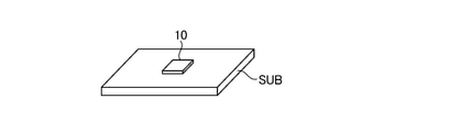
- FIG. 2 is a diagram showing how a semiconductor device is mounted on a substrate according to the first embodiment of the present disclosure.
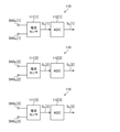
- FIG. 3 is a diagram showing an example of the internal configuration of the current detection circuit of FIG.
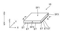
- FIG. 4 is an external perspective view of the semiconductor device observed from diagonally above according to the first embodiment of the present disclosure.
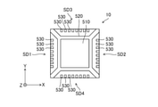
- FIG. 5 is a plan view of the semiconductor device observed from below according to the first embodiment of the present disclosure.
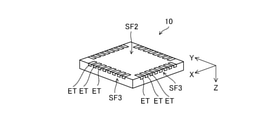
- FIG. 6 is an external perspective view of the semiconductor device observed from diagonally below according to the first embodiment of the present disclosure.
- FIG. 7 is a cross-sectional view of the semiconductor device according to the first embodiment of the present disclosure.
- FIG. 8 is a transmission plan view of the semiconductor device according to the first embodiment of the present disclosure.
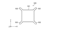
- FIG. 9 is a plan view of the die pad according to the first embodiment of the present disclosure.
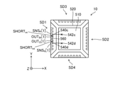
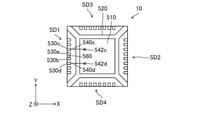
- FIG. 10A is a transmission plan view of the semiconductor device according to the embodiment EX1_1 belonging to the first embodiment of the present disclosure (case with one sense wire).
- FIG. 10B is a transmission plan view of the semiconductor device according to the embodiment EX1_1 belonging to the first embodiment of the present disclosure (case with one sense wire).
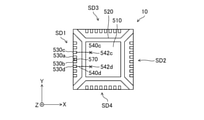
- FIG. 11 is a transmission plan view of the semiconductor device according to the embodiment EX1_1 belonging to the first embodiment of the present disclosure (note the external terminal).
- FIG. 10A is a transmission plan view of the semiconductor device according to the embodiment EX1_1 belonging to the first embodiment of the present disclosure (case with one sense wire).
- FIG. 10B is a transmission plan view of the semiconductor device according to the embodiment EX1_1 belonging to the first embodiment of the present disclosure (case with one sense wire).
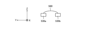
- FIG. 12 is a diagram showing the relationship between the sense wire and the two leads according to the embodiment EX1_1 belonging to the first embodiment of the present disclosure.
- FIG. 13 is a transmission plan view of a semiconductor device according to Example EX1_1 belonging to the first embodiment of the present disclosure (case with two sense wires).
- FIG. 14 is a transmission plan view of a semiconductor device according to Example EX1_1 belonging to the first embodiment of the present disclosure (case with three sense wires).
- FIG. 15 is a diagram showing the relationship between the external terminal of the semiconductor device and the wiring pattern on the substrate according to the embodiment EX1_1 belonging to the first embodiment of the present disclosure.
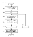
- FIG. 16 is a flowchart of a test process according to Example EX1_2 belonging to the first embodiment of the present disclosure.
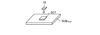
- FIG. 17 is a diagram showing a relationship between a test substrate, a socket, and a semiconductor device in a test process according to Example EX1_2 belonging to the first embodiment of the present disclosure.
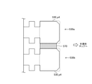
- FIG. 18 is a plan view of each lead according to Example EX1_3 belonging to the first embodiment of the present disclosure.
- FIG. 19 is a diagram showing how the two leads are connected by two sense wires according to the embodiment EX1_3 belonging to the first embodiment of the present disclosure.
- FIG. 20 is a diagram showing how the two leads are connected by four sense wires according to the embodiment EX1_3 belonging to the first embodiment of the present disclosure.
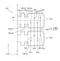
- FIG. 21 is a plan view of a plurality of leads related to current detection and their surroundings, which are provided in comparison with the first embodiment.
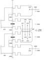
- FIG. 22 is a plan view of a plurality of leads related to current detection and their surroundings, which are provided in comparison with the first embodiment, and is a diagram showing a current flow.
- FIG. 23 is a plan view of a plurality of leads and their surroundings related to current detection according to Example EX1_4 belonging to the first embodiment of the present disclosure, and is a diagram showing a current flow.
- FIG. 24 is a transmission plan view of the semiconductor device according to the second embodiment of the present disclosure.
- FIG. 25 is a transmission plan view of the semiconductor device according to the third embodiment of the present disclosure.
- FIG. 26 is a plan view of the two leads and the connecting metal portion according to the third embodiment of the present disclosure.
- FIG. 27 is a transmission plan view of a modified semiconductor device according to the third embodiment of the present disclosure.
- the ground refers to a reference conductive portion having a reference potential of 0 V (zero volt) or refers to the potential of 0 V itself.
- the reference conductive portion is formed of a conductor such as metal.
- the potential of 0V may be referred to as a ground potential.
- the voltage shown without any particular reference represents the potential seen from ground.
- Level refers to the level of potential, where a high level has a higher potential than a low level for any signal or voltage of interest.
- the on state refers to the state in which the drain and source of the transistor are conducting, and the off state means the drain and source of the transistor. Refers to a state in which the interval is non-conducting (blocked state).
- MOSFETs are understood to be enhancement-type MOSFETs.
- MOSFET is an abbreviation for "metal-oxide-semiconductor field-effect transistor".
- the on state and the off state of any transistor may be simply expressed as on and off.
- FIG. 1 shows the overall configuration of the motor drive system SYS according to the first embodiment.
- the motor drive system SYS includes a semiconductor device 10 that functions as a motor control device, an inverter circuit 20, a three-phase motor 30, and a host circuit 40 formed by an MPU (Micro Processing Unit) or the like.
- MPU Micro Processing Unit
- the three-phase motor 30 is a three-phase brushless synchronous motor including coils L [1], L [2], and L [3] for three phases connected by a star.
- the coils L [1], L [2] and L [3] correspond to the U-phase, V-phase and W-phase coils, respectively, and in the present embodiment, the U-phase, V-phase and W-phase are respectively. It is referred to as a first phase, a second phase, and a third phase.
- the circuit configuration corresponding to the first phase, the circuit configuration corresponding to the second phase, and the circuit configuration corresponding to the third phase are common to each other. Therefore, the configuration of each circuit and the like will be described below using the symbol i representing an arbitrary integer as appropriate.
- the circuit, element, physical quantity, etc. referred to by the symbol including the symbol “[i]” represents the circuit, element, physical quantity, etc. in the phase i.
- the three-phase motor 30 has a stator and a rotor provided with a permanent magnet, and the stator is provided with coils L [1], L [2] and L [3].
- One end of the coil L [1] is commonly connected to the external terminals OUT O [1], SNS N [1] and OUT MNT [1] described later through the external wiring WR O [1].
- One end of the coil L [2] is commonly connected to the external terminals OUT O [2], SNS N [2] and OUT MNT [2] described later through the external wiring WR O [2].
- One end of the coil L [3] is commonly connected to the external terminals OUT O [3], SNS N [3] and OUT MNT [3] described later through the external wiring WR O [3].
- the other ends of the coils L [1] to L [3] are commonly connected at the neutral point NP.
- External wiring WR O [1] to WR O [3] and WR IN [1] to WR IN [3] described later are wiring provided outside the semiconductor device 10, and are substrates on which the semiconductor device 10 is mounted. Includes wiring patterns on (board SUB described below).
- FIG. 2 shows a substrate SUB on which the semiconductor device 10 is mounted. However, in FIG. 2, among the parts mounted on the substrate SUB, the parts other than the semiconductor device 10 are omitted, and the wiring pattern is also omitted.
- coil currents IL [1], IL [2], and IL [3] are referred to as coil currents IL [1], IL [2], and IL [3], respectively. If the power regeneration by the three-phase motor 30 is ignored, the coil currents IL [1], IL [2], and IL [3] are the external terminals OUT O [1], OUT O [2], and OUT O [, respectively. 3] flows toward the neutral point NP. In the following, unless otherwise specified, the coil current IL [1] is assumed to flow from the external terminal OUT O [i] toward the neutral point NP.
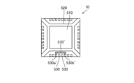
- the semiconductor device 10 is formed by enclosing and sealing a semiconductor chip on which a semiconductor integrated circuit is formed in a package made of a sealing resin, and a plurality of external terminals are exposed and provided in the package of the semiconductor device 10. There is.
- the coil current is passed External terminals OUT IN [1] to OUT IN [3] and OUT O [1] to OUT O [3], and external terminals for coil current detection SNS P [1] to SNS P [3] and SNS N [1] ] ⁇ SNS N [3], external terminals OUT MNT [1] to OUT MNT [3] for coil terminal voltage monitoring, and external terminals P HG [1] to P HG [3] and P for gate signal output.
- the plurality of external terminals include a communication terminal group composed of two or more external terminals, and include a semiconductor device 10 (control circuit 120 described later) and a device. Communication between the host circuits 40 is performed via the communication terminal group. Further, other external terminals may be provided in the semiconductor device 10.
- the inverter circuit 20 includes a first-phase half-bridge circuit 210 [1], a second-phase half-bridge circuit 210 [2], and a third-phase half-bridge circuit 210 [3], and is a semiconductor device 10.
- the coil currents IL [1] to IL [3] are supplied to the coils L [1] to L [3] under the control of.
- Each of the half-bridge circuits 210 [1], 210 [2] and 210 [3] consists of a high-side transistor and a low-side transistor connected in series between the line to which the power supply voltage VM is applied and the ground.
- the power supply voltage VM is a predetermined positive DC voltage.
- the high-side transistor and the low-side transistor are configured as an N-channel MOSFET (Metal Oxide Semiconductor Field effect transistor).
- the high-side transistor and the low-side transistor provided in the half-bridge circuit 210 [i] are referred to by MH [i] and ML [i], respectively.
- the drain of the high-side transistor MH [i] is connected to the power supply terminal to which the power supply voltage VM is applied to receive the power supply voltage VM, and is supplied to the high side.
- the source of the transistor MH [i] and the drain of the low-side transistor ML [i] are commonly connected by the node ND [i], and the source of the low-side transistor ML [i] is connected to the ground.
- connection node ND [1] between the transistors MH [1] and ML [1] is commonly connected to the external terminal OUT IN [1] and the SNS P [1] through the external wiring WR IN [1].
- the connection node ND [2] between the transistors MH [2] and ML [2] is commonly connected to the external terminal OUT IN [2] and SNS P [2] through the external wiring WR IN [2].
- the connection node ND [3] between the transistors MH [3] and ML [3] is commonly connected to the external terminal OUT IN [3] and SNS P [3] through the external wiring WR IN [3].
- the semiconductor device 10 includes a current detection circuit 10, a control circuit 120, a predriver circuit 130, an internal power supply circuit 140, a charge pump circuit 150, a calibration information holding unit 160, and a sense resistor R SNS [1]. It includes R SNS [2] and R SNS [3].
- the power supply voltage VM is supplied to the external terminal PVM from the outside of the semiconductor device 10. Outside the semiconductor device 10, a capacitor C CPA is provided between the external terminals P VCP and P VM , and a capacitor C CPB is provided between the external terminals CP1 and CP2.
- the charge pump circuit 150 is connected to the external terminals CP1, CP2, P VCP and P VM, it generates a power supply voltage VCP by boosting the power supply voltage VM by using a capacitor C CPA and C CPB.
- the power supply voltage VCP is a DC voltage higher than the power supply voltage VM (for example, a DC voltage higher by 5 V).
- the voltage of the potential difference between the power supply voltage VM and the VCP is applied between both ends of the capacitor C CPA , and the power supply voltage VCP is generated at the external terminal P VCP.
- the internal power supply circuit 140 generates one or more internal power supply voltages based on the power supply voltage VM. Each circuit in the semiconductor device 10 is driven based on the internal power supply voltage.
- the sense resistor R SNS [i] is a resistance for detecting the coil current IL [i] provided in the semiconductor device 10. Therefore, one end and the other end of the sense resistor R SNS [1] are connected to the external terminals OUT IN [1] and OUT O [1], respectively, and one end and the other end of the sense resistor R SNS [2] are connected to each other. , Each connected to the external terminals OUT IN [2] and OUT O [2], and one end and the other end of the sense resistor R SNS [3] are connected to the external terminals OUT IN [3] and OUT O [3], respectively. Connected to.
- the external terminal OUT IN [1] and the SNS P [1] are short-circuited by a part of the external wiring WR IN [1], and the external terminal OUT O [1] and the SNS N [1] are short-circuited. ] Is short-circuited by a part of the external wiring WR O [1].
- the second phase and the third phase That is, the external terminals OUT IN [i] and the SNS P [i] are short-circuited by a part of the external wiring WR IN [i], and the external terminals OUT O [i] and the SNS N [i] are short-circuited. It is short-circuited by a part of the external wiring WR O [i].
- the i-th phase the voltage drop corresponding to the coil current IL [i] is generated in the sense resistor R SNS [i] by flowing the coil current IL [i] is the sense resistor R SNS [i] ,
- the voltage drop in the sense resistor R SNS [i] is applied between the external terminals SNS P [i] and SNS N [i].
- the external terminals SNS P [i] and OUT IN [i] are short-circuited in the package of the semiconductor device 10, and the external terminals SNS N [i] and OUT O [ Although i] are short-circuited, the configuration for realizing these short-circuits will be described later.
- the current detection circuit 110 is connected to the external terminals SNS P [1] to SNS P [3] and SNS N [1] to SNS N [3], and is connected between the external terminals SNS P [1] and SNS N [1].
- Coil current IL [1] is detected based on the voltage
- coil current IL [2] is detected based on the voltage between the external terminals SNS P [2] and SNS N [2]
- external terminals SNS P [3] and SNS external terminals SNS P [3] and SNS.
- the coil current IL [3] is detected based on the voltage between N [3].
- the detection of the coil current IL [i] is the detection of the current value of the coil current IL [i], and the detection current values of the coil currents IL [1], IL [2], and IL [3] by the current detection circuit 110 are detected.
- the detected current values are referred to as VAL_IL [1], VAL_IL [2], and VAL_IL [3], respectively.
- Signals IL_DET representing the detected current values VAL_IL [1], VAL_IL [2] and VAL_IL [3] are sent from the current detection circuit 110 to the control circuit 120.
- the signal IL_DET is generated with reference to the calibration information held by the calibration information holding unit 160, and the calibration information will be described later.
- the current detection circuit 110 includes current sensors 111 [1] and ADC 112 [1] for the first phase, and current sensors 111 [2] and ADC 112 [2] for the second phase. 2] and a current sensor 111 [3] and an ADC 112 [3] for the third phase.
- Current sensor 111 [i] is connected to the external terminal SNS P [i] and SNS N [i], a voltage value proportional to the external terminal SNS P [i] and SNS N [i] between the voltage (potential difference) as an analog voltage signal having outputs an analog signal S a [i].
- the current sensor 111 [i] can be configured by an amplifier circuit including an operational amplifier.
- the ADC 112 [i] is an analog-to-digital converter, and generates a digital signal S D [i] by analog-digital conversion of the analog signal S A [i].
- the digital signal S D [i] has a signal value proportional to the voltage (potential difference) between the external terminals SNS P [i] and the SNS N [i], and the signal value of the digital signal S D [i] is the detection current value.
- VAL_IL [i] corresponds to VAL_IL [i].
- the digital signals SD [1] to SD [3] are generated by the three analog-to-digital converters (that is, ADC 112 [1] to 112 [3]), but the current is generated.
- analog to the detection circuit 110 - digital converter may be provided only one single analogue - the one analog by using a time division digital converter - analog signal S a [1] at digital converters ⁇ S
- the digital signals S D [1] to S D [3] may be generated from A [3].
- the control circuit 120 generates a drive control signal DRV for rotationally driving the three-phase motor 30 based on the signal IL_DET and the motor drive command signal supplied from the host circuit 40, and generates the generated drive control signal DRV. Output to the pre-driver circuit 130.
- the pre-driver circuit 130 is connected to the external terminals OUT MNT [1] to OUT MNT [3], P HG [1] to P HG [3], P LG [1] to P LG [3], and P GND. .. External terminal OUT MNT [1] ⁇ OUT MNT [3] , as described above, respectively, connected to one end of the coil L [1] ⁇ L [3 ] through the external wiring WR O [1] ⁇ WR O [3] Will be done.
- the external terminals PHG [1] to PHG [3] and PLG [1] to PLG [3] are the transistors MH [1] to MH [3] and ML [1], respectively, through other external wiring (not shown).
- the pre-driver circuit 130 refers to the voltages of the external terminals OUT MNT [1] to OUT MNT [3], and the gate signals HG [1] to HG [3] and LG [1] to LG based on the drive control signal DRV.
- LG [3] is generated, and the gate signals HG [1] to HG [3] and LG [1] to LG [3] are transmitted to the transistors MH [1] to MH [3] and ML [1] to ML, respectively.
- those transistors are turned on / off individually.
- the gate signals HG [1] to HG [3] and LG [1] to LG [3] each take a high level or low level signal level.
- the high-level potentials differ from each other between the gate signals HG [i] and LG [i]
- the low-level potentials also differ from each other.
- the gate signal HG [i] is set to a high level, the transistor MH [i] is turned on, and when the gate signal HG [i] is set to a low level, the transistor MH [i] is turned off.
- the high-level gate signal HG [i] is formed by using the power supply voltage VCP.
- the control circuit 120 receives a motor drive command signal from the host circuit 40 and specifies that the three-phase motor 30 rotates at the rotation speed specified by the motor drive command signal or by the motor drive command signal.
- the three-phase motor 30 can be vector-controlled based on the detected current values VAL_IL [1], VAL_IL [2], and VAL_IL [3] so that the torque to be generated is generated by the three-phase motor 30.
- the drive control signal DRV for realizing the vector control to the pre-driver circuit 130, for example, the three-phase motor 30 is driven by a sine wave.
- the semiconductor device 10 has a package called QFN (Dual Flatpack No-leaded).
- QFN Double Flatpack No-leaded
- the package described in this embodiment refers to the package of the semiconductor device 10.
- a three-dimensional Cartesian coordinate system consisting of X-axis, Y-axis, and Z-axis that are orthogonal to each other is assumed, and the direction from the negative side to the positive side of the Z-axis is defined as upward, and the opposite direction is defined as downward. ..
- a plane parallel to the X-axis and the Y-axis is referred to as an XY plane
- a plane parallel to the Y-axis and the Z-axis is referred to as a YZ plane
- a plane parallel to the Z-axis and the X-axis is referred to as a ZX plane.
- the package has a rectangular parallelepiped outer shape, and the rectangular parallelepiped as the outer shape of the package includes an upper surface SF1 and a lower surface SF2 parallel to the XY plane, and four side surface SF3s.
- the upper surface SF1 and the lower surface SF2 are two surfaces facing each other, and the upper surface SF1 is located on the positive side of the Z axis with respect to the lower surface SF2.
- the four side surface SF3s are composed of two side surface SF3s parallel to the YZ plane and facing each other, and two side surface SF3s parallel to the ZX plane and facing each other.
- FIG. 4 is an external perspective view of the semiconductor device 10 when the upper surface SF1 and the two side surface SF3s are observed from the positive side of the Z axis.
- FIG. 5 is a plan view of the semiconductor device 10 when the lower surface SF2 is observed from the negative side of the Z axis.
- FIG. 6 is an external perspective view of the semiconductor device 10 when the lower surface SF2 and the two side surface SF3s are observed from the negative side of the Z axis.
- the outer shape of the package is a quadrangle, and the four sides of the quadrangle are referred to as sides SD1 to SD4 (see FIG. 5).
- the sides SD1 and SD2 are two sides facing each other, and both are parallel to the Y axis.
- the sides SD3 and SD4 are two sides facing each other and both parallel to the X-axis.
- the reference numeral “ET” represents an external terminal provided in the semiconductor device 10.
- the number of external terminals ET provided in the semiconductor device 10 is 32.
- the number of external terminal ETs provided in the semiconductor device 10 is arbitrary.
- the reference numeral “ET” is attached only to some of the external terminals in order to prevent the illustration from becoming complicated.
- a total of 32 external terminal ETs are a first external terminal row arranged along the side SD1, a second external terminal row arranged along the side SD2, and a third external arranged along the side SD3. It is composed of a terminal row and a fourth external terminal row arranged along the side SD4, and each external terminal row is composed of eight external terminal ETs. In each external terminal row, the eight external terminal ETs are arranged side by side at equal intervals. Each external terminal ET is a metal terminal exposed from the package, and is mainly exposed from the lower surface SF2.
- each external terminal ET in the first external terminal row is exposed from the package from the lower surface SF2 to the side surface SF3 corresponding to the side SD1
- each external terminal ET in the second external terminal row corresponds to the lower surface SF2 to the side SD2. It is exposed from the package over the side surface SF3.
- 26 external terminal ETs are the external terminals CP1, CP2, PVCP , PVM , OUT IN [1] to OUT IN [3], OUT O [shown in FIG.
- FIG. 7 is a cross-sectional view of the semiconductor device 10 when the semiconductor device 10 is cut along the cutting line AA shown in FIG. 4 (that is, a cross-sectional view of the semiconductor device 10 with a cross section parallel to the ZX plane).
- FIG. 7 is a schematic cross-sectional view showing the positional relationship of the components of the semiconductor device 10, and the detailed shape of each component may differ from the actual shape.
- the semiconductor device 10 is for a plurality of chips for connecting (electrically connecting) the semiconductor chip 510, the die pad 520 supporting the semiconductor chip 510, the plurality of leads 530, and the semiconductor chip 510 and the plurality of leads 530.
- a wire 540 and a sealing resin 550 are provided.
- the wire 540 corresponds to what is generally called a bonding wire, but is referred to as a chip wire for clear distinction from the sense wire described later.
- the sealing resin 550 collectively seals a semiconductor chip 510, a die pad 520, each lead 530, a wire 540 for each chip, and a metal body for sense (sense wire 560, etc .; not shown in FIG. 7) described later. It is an insulating material, and the package of the semiconductor device 10 is formed by the sealing resin 550. However, the package is formed so that a part of each of the plurality of leads 530 is exposed from the sealing resin 550. Specifically, all or part of the lower surface 531 of each lead 530 is exposed from the lower surface of the sealing resin 550 (hence, the lower surface SF2 of the package), and all or part of the side surface 532 of each lead 530 is also the sealing resin 550. (Therefore, the side surface SF3 of the package) is exposed.
- the semiconductor chip 510 is a component in which a semiconductor integrated circuit is formed on a semiconductor substrate, and the semiconductor device 10 includes blocks 110, 120, 130, 140, 150, and 160 shown in FIG. 1 by the semiconductor integrated circuit in the semiconductor chip 510. Each circuit in is formed. However, although the details will be described later, the sense resistors R SNS [1] to R SNS [3] are formed outside the semiconductor chip 510.
- the semiconductor chip 510 is die-bonded on the die pad 520 with the surface (surface) on the side on which each functional element is formed facing upward. Further, on the surface of the semiconductor chip 510, a plurality of pads (not shown) are formed by exposing a part of the wiring layer from the surface protective layer.
- Each pad is connected to the corresponding lead 530 via a chip wire 540. That is, the semiconductor chip 510 and the plurality of leads 530 are connected via the wires 540 for the plurality of chips.
- the connection via the wire 540 for the chip or the connection by the wire 540 for the chip naturally means an electrical connection.
- the die pad 520 is composed of a thin metal plate having a thickness direction in the Z-axis direction.
- the entire die pad 520 is sealed with the sealing resin 550, but the semiconductor device 10 is such that the lower surface of the die pad 520 is exposed from the lower surface of the sealing resin 550 (hence, the lower surface SF2 of the package). May be configured.
- a retaining portion (not shown) for preventing the die pad 520 from coming off from the sealing resin 520 is formed on the die pad 520.
- FIG. 8 is a transmission plan view of the semiconductor chip 510, the die pad 520, and each lead 530 assuming that the sealing resin 550 is transparent (actually, the sealing resin 550 is opaque).
- the transmission plan view of FIG. 8 is a transmission plan view when the semiconductor device 10 is observed from the positive side of the Z axis.
- components other than the semiconductor chip 510, the die pad 520, and each lead 530 are not shown.
- the outermost rectangle represents the outer edge of the package.
- the reference numeral “530” is attached to only some of the leads in order to prevent the illustration from becoming complicated.
- Each of the semiconductor chip 510 and the die pad 520 has a substantially quadrangular shape in a plan view.
- the die pad 520 is provided with a total of four suspension leads 522 extending from each apex of the quadrangle to the corresponding corner of the package to the main body 521 having a quadrangular shape in a plan view.
- the quadrangle of the die pad 520 is larger than the quadrangle of the semiconductor chip 510, and the entire semiconductor chip 510 is placed on the surface of the die pad 520.
- the plan view means observing the observation target from above along the Z axis.
- Eight leads 530 are provided on the positive side of the X-axis, the negative side of the X-axis, the positive side of the Y-axis, and the negative side of the Y-axis when viewed from the center of the semiconductor chip 510 or the center of the die pad 520. ing. That is, a total of 32 leads 530 are dispersedly arranged around the semiconductor chip 510 and the die pad 520.
- a total of 32 leads 530 include a first lead row arranged along the side SD1, a second lead row arranged along the side SD2, and a third lead row arranged along the side SD3. It is composed of a fourth lead row arranged along the side SD4, and each lead row is composed of eight leads 530. In each lead row, the eight leads 530 are arranged side by side at equal intervals.
- Each lead 530 is composed of a metal part that fits inside the package and a metal part that is exposed from the package.
- the former metal part is called an inner lead, while the latter metal part is called an outer lead.
- the outer lead functions as the corresponding metal terminal ET.
- the outer lead protrudes from the package as a pin-shaped metal terminal ET.
- Eight leads 530 forming the first lead row constitute eight external terminal ETs forming the first external terminal row, and eight leads 530 forming the second lead row form the second external terminal row 8
- Two external terminals ET are configured. The same applies to the third and fourth lead rows.
- Each lead 530 is composed of a thin metal plate having a thickness direction in the Z-axis direction.
- the shape of each lead 530 in a plan view is approximately a quadrangle, but the shape of each lead 530 in a plan view may be arbitrary.
- the material of the lead 530 is copper.
- the lead 530 may be formed by using a metal other than copper.
- the lead 530 may be formed of a so-called 42 alloy (an alloy in which nickel is mixed with iron).
- the material of the die pad 520 may be the same as the material of the lead 530.
- Each lead 530 is formed with a retaining portion 533 to prevent each lead 530 from coming out of the package (see FIG. 7). Further, although not clear from FIGS. 7 and 8, a metal-plated layer having solder wettability is formed on the exposed portion of each lead 530.
- the wire 540 for chips is a metal wire made of gold, aluminum or copper.
- each chip wire 540 one end of the chip wire 540 is connected to a desired pad on the semiconductor chip 510, and the other end of the chip wire 540 is connected to a desired position on the desired lead 530.
- the pad and the desired lead 530 are electrically connected via a wire 540 for the tip.
- the connection point between the lead 530 and the chip wire 540 (the point where the chip wire 540 is wire-bonded to the lead 530) is on the inner lead.
- the first embodiment includes the following Examples EX1_1 to EX1_6.
- the characteristic configurations related to the sense resistors R SNS [1] to R SNS [3] of FIG. 1 will be mainly described.
- the above-mentioned matters in the first embodiment are applied to the following Examples EX1_1 to EX1_6 unless otherwise specified and without contradiction, and in each embodiment, the matters inconsistent with the above-mentioned matters in the first embodiment are described.
- the description in each embodiment may be prioritized. Further, as long as there is no contradiction, the matters described in any of the examples EX1_1 to EX1_6 can be applied to any other embodiment (that is, any two or more implementations in the plurality of examples). It is also possible to combine examples).
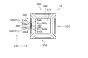
- FIG. 10A is a transmission plan view of the semiconductor device 10 assuming that the sealing resin 550 is transparent.
- the transmission plan view of FIG. 10A is a transmission plan view when the semiconductor device 10 is observed from the positive side of the Z axis.
- FIG. 10A only the parts necessary for explaining the technique related to the embodiment EX1_1 are shown, and the illustration of some components of the semiconductor device 10 is omitted (also in FIGS. 11, 13, and 14 described later). Similarly).
- the outermost rectangle represents the outer edge of the package (also in FIGS. 11, 13, 14, 25 and 27 described later). Further, in FIG.
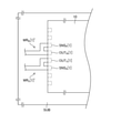
- FIG. 10A is an enlarged view of a part of FIG. 10A.
- the reference numerals “530a”, “530b”, “530c” and “530d” are attached only to specific four leads among the plurality of leads 530 (FIGS. 13 and FIGS. 13 and FIGS. The same applies to 14).
- the wire 540 for the chip connecting the lead 530c and the semiconductor chip 510 is particularly referred to by the reference numeral "540c”
- the wire 540 for the chip connecting the lead 530d and the semiconductor chip 510 is particularly referred to by the reference numeral "540d”.
- FIG. 10B is an enlarged view of a part of FIG. 10A.
- Leads 530a to 530d are four leads 530 adjacent to each other provided with respect to the side SD1, and are arranged in the order of leads 530d, 530b, 530a, and 530c from the negative side to the positive side of the Y axis. .. That is, the leads 530a and 530b are adjacent to each other, the lead 530a is located between the leads 530b and 530c, and the lead 530b is located between the leads 530a and 530d.
- the leads 530a to 530d are the four leads 530 assigned to the first phase. Then, as can be understood from the comparison of FIGS.
- SNS N [1] is assigned. That is, the lead 530a forms the external terminal OUT IN [1], the lead 530b forms the external terminal OUT O [1], and the lead 530c forms the external terminal SNS P [1].
- the lead 530d forms an external terminal SNS N [1].
- the leads 530a and 530b are connected by a sense wire 560 in the package.
- the sense wire 560 is an example of a sense metal body that connects the leads 530a and 530b.
- the sense wire 560 is a metal wire constructed of gold, aluminum or copper.
- the material of the sense wire 560 may be the same as the material of the chip wire 540, and the thickness of the sense wire 560 (that is, the diameter of the cross section) may be the same as the thickness of the chip wire 540.
- FIG. 12 shows a side view of the leads 530a and 530b and the sense wire 560 observed along the X-axis direction.
- One end of the sense wire 560 is connected to a predetermined position on the upper surface of the lead 530a (hence, a predetermined position on the inner lead in the lead 530a), and the other end of the sense wire 560 is connected to a predetermined position on the upper surface of the lead 530b (hence, in the lead 530b). It is connected to a predetermined position on the inner lead).
- the connection between the sense wire and the lead is realized by well-known wire bonding as well as the connection between the wire for the chip and the lead.
- the sense wire 560 connects the leads 530a and 530b by the shortest route or a route close to the shortest route. At least, the sense wire 560 is not connected to the semiconductor chip 510, and thus connects between the leads 530a and 530b without going through the semiconductor chip 510.
- the connection via the sense wire 560 or the connection by the sense wire 560 naturally means an electrical connection.
- the number of sense wires 560 connecting between the leads 530a and 530b may be one, or may be any number of two or more. That is, for example, as shown in FIG. 13, two sense wires 560 may be used to connect the leads 530a and 530b, or as shown in FIG. 14, three sense wires 560 may be used to connect the leads 530a and 530b. You may connect.
- the lengths of the plurality of sense wires 560 are the same as each other.
- the lengths of the plurality of sense wires 560 may all be different from each other, or q kinds of lengths may be mixed in the lengths of p sense wires 560 (p is 3). Integer greater than or equal to: q is an integer less than p and greater than or equal to 2).
- Example EX1_1 it is assumed that between the lead 530a and 530b are connected by N A present sense wire 560.
- the N A is any integer of 1 or more.
- the parallel resistance value of the sense wire 560 of the book functions as the resistance value of the sense resistor R SNS [1].
- the resistance components of the leads 530a and 530b themselves are also included in the sense resistance R SNS [1], but the resistance value of each lead is negligibly small compared to the resistance value of the sense wire 560 (hence). Ignore it).
- FIG. 15 shows a schematic plan view of a part of the substrate SUB on which the semiconductor device 10 is mounted.
- a plurality of solder-coated lands are formed at necessary locations on the substrate SUB (lands are not shown in FIG. 15).
- the semiconductor device 10 is placed at a position where the surface of each land of the substrate SUB and each external terminal (lower surface of each lead) of the semiconductor device 10 face each other, and each external terminal (lower surface of each lead) is attached to the solder on each land.
- the semiconductor device 10 is mounted on the substrate SUB by performing reflow in the contacted state.
- a wiring pattern WR IN [1]' which is a part of the external wiring WR IN [1] shown in FIG.
- the wiring pattern WR O [1]' is formed.
- the land connected to the external terminal OUT IN [1] and the land connected to the external terminal SNS P [1] are short-circuited on the board SUB by the wiring pattern WR IN [1]', so that the external terminal OUT IN is short-circuited. [1] (hence the lead 530a) is shorted to the external terminal SNS P [1] (hence the lead 530c) through the external wiring WR IN [1]'.
- the land connected to the external terminal OUT O [1] and the land connected to the external terminal SNS N [1] are short-circuited on the board SUB by the wiring pattern WR O [1]', thereby externalizing.
- the terminal OUT O [1] (hence the lead 530b) is shorted to the external terminal SNS N [1] (hence the lead 530d) through the external wiring WR O [1]'.
- connection point 542c between the semiconductor chip 510 and the wire 540c for the chip and the connection point 542d between the semiconductor chip 510 and the wire 540d for the chip are the current detection circuit 110 formed on the semiconductor chip 510 (FIG. 10A). 1) is connected.
- the connection points 542c and 542d refer to points where the chip wire 540c and 540d are wire-bonded to the semiconductor chip 510, respectively.
- a voltage drop proportional to the coil current IL [1] occurs in the sense resistor R SNS [1] (here, NA sense wires 560), and the voltage drop occurs between the connection points 542c and 542d. A corresponding potential difference is generated.
- the current detection circuit 110 can detect the coil current IL [1] based on the potential difference between the connection points 542c and 542d, and obtain the above-mentioned detection current value VAL_IL [1]. It can be considered that the potential difference between the connection points 542c and 542d and the potential difference between the external terminals SNS P [1] and SNS N [1] are the same.
- the eight leads 530 arranged along the side SD1 four leads 530 located near the center are assigned to the leads 530a to 530d, but the eight leads 530 arranged along the side SD1 are assigned.
- which lead is assigned to the leads 530a to 530d is arbitrary.
- the leads 530a to 530d are arranged in the order of leads 530d, 530b, 530a, and 530c as described above.
- the leads 530d or 530c may be the leads 530 at the ends of the eight leads 530 arranged along the side SD1.
- the structure related to coil current detection has been described by focusing on the first phase, but the structure related to coil current detection in the second phase and the structure related to coil current detection in the third phase have been described.
- the structure is similar to that of the first phase, and the techniques described for the first phase also apply to the second and third phases.
- the symbols “[1]” in the above description of Example EX1_1 are replaced with the symbols “[2]”, and the leads 530a to 530d are arranged along, for example, the side SD3. Think of it as 530.
- the leads 530a to 530d are arranged along, for example, the side SD4 after replacing the symbol “[1]” in the above description of Example EX1_1 with the symbol “[3]”. Think of it as four leads 530.
- the semiconductor device 10 is provided with three sets of leads 530a to 530d, and the first set of leads 530a to 530d are provided with external terminals OUT IN [1], OUT O [1], SNS P [1] and SNS N [1], respectively.
- the second set of leads 530a to 530d are assigned to the external terminals OUT IN [2], OUT O [2], SNS P [2] and SNS N [2], respectively, and the third set of leads 530a to 530d are assigned to. Assigned to the external terminals OUT IN [3], OUT O [3], SNS P [3], and SNS N [3], respectively.
- the first set of leads 530a to 530d, the second set of leads 530a to 530d, and the third set of leads 530a to 530d are typically arranged on different sides of the semiconductor device 10. Of the total of 12 leads, a plurality of leads belonging to different sets may be arranged on a common side.
- the current detection circuit 110 detects the coil current IL [1] based on the potential difference between the leads 530c and 530d of the first set (potential difference between the connection points 542c and 542d for the first set), and detects the above-mentioned detected current value VAL_IL. [1] can be obtained, and the coil current IL [2] is detected based on the potential difference between the leads 530c and 530d of the second set (the potential difference between the connection points 542c and 542d for the second set), and the above-mentioned detection is performed.
- the current value VAL_IL [2] can be obtained, and the coil current IL [3] is detected based on the potential difference between the leads 530c and 530d of the third set (the potential difference between the connection points 542c and 542d for the third set).
- the above-mentioned detected current value VAL_IL [3] can be obtained.
- the distance between the centers of two leads 530 adjacent to each other on the sides SD1, SD2, SD3 or SD4 is 500 ⁇ m (micrometer). It is assumed that the cross-sectional shape of the sense wire 560 is circular, the diameter of the sense wire 560 in the cross section is 30 ⁇ m, and the sense wire 560 is made of copper. In this case, assuming that the sense wire 560 having a length of 500 ⁇ m is used, the resistance value (resistance value between both ends) of one sense wire 560 is about 12.5 m ⁇ . The parallel resistance value of the two sense wires 560 is about 6.25 m ⁇ , and the parallel resistance value of the three sense wires 560 is about 4.16 m ⁇ .
- the power consumption of the sense resistance R SNS [i] of each phase is about 1.23 W from “14A ⁇ 14A ⁇ 6.25 m ⁇ 1.23”, and the sense resistance R SNS [1] to R SNS.
- the total power consumption in [3] is about 3.7 W.
- it is generally within the allowable power consumption of a general QFN package of about 5 mm square (representing the maximum allowable amount of power consumption in the package and also referred to as package power).
- package power Taking into consideration the balance with the required precision and package power for the detection of the coil current IL [i], may be adjusted to the diameter of the number of the sense wire 560 (i.e. N value of A) or sense wire 560 ..
- a detection resistor (resistance of about 10 m ⁇ ) is applied to a semiconductor device in order to detect a coil current (especially a relatively large coil current such as a coil current of 10 A or more). Connect externally. At this time, the resistance value of the detection resistance externally connected to the semiconductor device varies, and the variation in the resistance value of the detection resistance deteriorates the detection accuracy of the coil current, which in turn deteriorates the desired motor control (for example, vector control). Hinders the realization of.
- the sense resistor R SNS [i] corresponding to the detection resistor is connected to the sense metal body (here, one or more senses) connecting the leads. It is formed with a wire 560).
- the resistance value of the sense metal body here, one or more sense wires 560
- the external calibration information based on the measurement result is used.
- the resistance value of the sense resistor R SNS [i] can be adjusted by adjusting the number of the sense wire 560 (i.e., the value of N A), which Alternatively or in addition, the resistance value of the sense resistance R SNS [i] can be adjusted by adjusting the diameter of the sense wire 560. By these adjustments, the required detection accuracy of the coil current IL [i] can be ensured while considering the package power.
- the following second virtual configuration is also considered.
- the lead 530a and the semiconductor chip 510 are connected by a wire for the first chip, and the lead 530b and the semiconductor chip 510 are connected by a wire for the second chip, and the semiconductor chip 510 and the wire for the first chip are connected.
- the connection point between them and the connection point between the semiconductor chip 510 and the wire for the second chip are connected on the semiconductor chip 510.
- the sense resistance R SNS [i] can be configured by the series resistance of the wires for the first and second chips.
- the length of the wire for forming the sense resistance R SNS [i] is longer (for example, several times longer) than in the configuration shown in FIG. 10A or the like, and the consumption by the wire is increased. The power is too high.
- there is concern that the heat generated by the wire will have a large effect on the semiconductor integrated circuit.
- the lead-to-lead short circuit technique is applied to the semiconductor device 10 according to the embodiment EX1_1.
- the leads 530a and 530c are short-circuited and the leads 530b and 530d are short-circuited without passing through the semiconductor chip 510 in the package.
- the semiconductor device 10 according to the embodiment EX1_1 to which the lead-to-lead short circuit technique is applied has the leads 530a and 530c without passing through the semiconductor chip 510 in the package.
- a short-circuiting metal body SHORT ac for short-circuiting between the leads and a short-circuiting metal body SHORT bd for short-circuiting between the leads 530b and 530d without passing through the semiconductor chip 510 in the package are provided.
- each short-circuit metal body is represented by a shaded area.
- the short-circuit metal body SHORT ac is a metal body that integrally bonds the leads 530a and 530c.
- the short-circuit metal body SHORT ac is made of the same material as the leads 530a and 530c.
- the short-circuit metal body SHORT ac is represented by a shaded area, and it is as if a boundary exists between the lead 530a or the lead 530c and the short-circuit metal body SHORT ac.
- the lead 530a, the short-circuit metal body SHORT ac, and the lead 530c may be formed by an integral metal flat plate having no such boundary.
- a single lead is composed of the one-piece metal flat plate, and the lead 530a and the lead 530c are formed by the single lead.
- the length (thickness) of the short-circuit metal body SHORT ac in the Z-axis direction may be the same as the length (thickness) of the leads 530a and 530c (particularly, the metal portions 530_p4 of the leads 530a and 530c) in the Z-axis direction. ..
- the short-circuit metal body SHORT bd is a metal body that integrally bonds the leads 530b and 530d.
- the short-circuit metal body SHORT bd is made of the same material as the leads 530b and 530d.
- the short-circuit metal body SHORT bd is represented by a shaded area, and it is as if a boundary exists between the lead 530b or the lead 530d and the short-circuit metal body SHORT bd.
- the lead 530b, the short-circuit metal body SHORT bd, and the lead 530d may be formed by an integral metal flat plate having no such boundary. It can also be considered that a single lead is composed of the one-piece metal flat plate, and the lead 530b and the lead 530d are formed by the single lead.
- the length (thickness) of the short-circuit metal body SHORT bd in the Z-axis direction may be the same as the length (thickness) of the leads 530b and 530d (particularly, the metal portions 530_p4 of the leads 530b and 530d) in the Z-axis direction. ..
- the length (thickness) of the short-circuit metal bodies SHORT ac and SHORT bd in the Z-axis direction is sufficiently larger than the diameter (for example, 30 ⁇ m) of each sense wire 560 (for example, 200 ⁇ m), and the short-circuit in the X-axis direction is short-circuited.
- the length (width) of the metal bodies SHORT ac and SHORT bd is also sufficiently larger than the diameter of each sense wire 560.
- the lead in 530a ⁇ alignment direction of 530d (Y axis direction), the resistance value per unit of each length of the short-circuiting metal member SHORT ac and SHORT bd the sense resistor composed of N A book sensing wire 560 It is sufficiently smaller than the resistance value per unit length of R SNS [i] (small enough to be ignored).
- N A denotes an arbitrary integer of 1 or more.
- the lengths of the short-circuit metal bodies SHORT ac and SHORT bd are shorter than the length of each sense wire 560.
- the short-circuit metal body SHORT ac and SHORT resistance values of bd for example, about 10Myuomega
- a present sense wire 560 for example, about 5 m [Omega) Small enough.
- Example EX1_2 >> Example EX1_2 will be described.
- Example EX1_2 an accurate detection method of the coil current using the calibration information will be described.
- FIG. 16 is a flowchart of a test process for acquiring and recording calibration information. The test process is incorporated as part of the shipping inspection process of the semiconductor device 10.
- the test board SUB TSET of FIG. 17 is prepared separately from the board 10 of FIG. 2, and the semiconductor device 10 is put into a test state.
- a socket SCT for mounting the semiconductor device 10 is mounted on the test board SUB TSET.
- the semiconductor device 10 is mounted on the socket SCT.
- each external terminal of the semiconductor device 10 conducts with the corresponding wiring pattern on the test board SUB TSET through the socket SCT (the wiring pattern is not shown in FIG. 17).
- test board SUB SET is formed on the test board SUB SET , and in the test state, the test board SUB SET.
- the wiring pattern of the external terminals OUT IN [i] and SNS P [i] is short-circuited, and the external terminals OUT O [i] and SNS N [i] are short-circuited.
- the test substrate SUB TSET is formed so that the required current can be supplied to the sense resistor R SNS [i] of each phase of the semiconductor device 10.
- step S13 in the test state, a predetermined test current ITSET is supplied to the sense resistor R SNS [i] (that is, a test current ITSET is passed between the external terminals OUT IN [i] and OUT O [i]). .. It is assumed that the test current ITSET is a direct current (for example, 10 A) flowing from the external terminal OUT IN [i] to the external terminal OUT O [i].
- step S14 the test circuit (not shown) in the semiconductor device 10 is an external terminal SNS P [i] and SNS when the test current ITSET is supplied to the sense resistor R SNS [i]. detecting a voltage between N [i] as the voltage V TEST [i], acquires calibration information of the i-phase based on the voltage V TEST [i].
- the test circuit is a circuit formed on the semiconductor chip 510 and operates significantly only in the test state. The acquisition of the phase i calibration information may be realized by the test circuit and the circuit on the test board SUB TSET in cooperation with each other.
- the calibration information holding unit 160 non-volatilely holds the calibration information of the first to third phases written in step S17.
- the calibration information holding unit 160 is composed of a non-volatile memory (for example, OTPROM (one time programmable read only memory)).
- the calibration information of each phase may be held non-volatilely by using a well-known method such as a Zener zap method, a polysilicon fuse method, or a laser cut method.
- a well-known method such as a Zener zap method, a polysilicon fuse method, or a laser cut method.
- the phase i calibration information is preset information based on the resistance value (actual resistance value) of the sense resistance R SNS [i]. I will explain this.
- step S14 of FIG. 16 the calibration information of the phase i based on the actual resistance value R REAL [i] is acquired.
- the semiconductor device 10 after the shipping inspection process including the test process is mounted on the substrate 10 as shown in FIG. 2 and then incorporated into the motor drive system SYS.
- the state in which the semiconductor device 10 is incorporated in the motor drive system SYS may be referred to as an actual operating state in order to clearly distinguish it from the above-mentioned test state.
- the semiconductor device 10 is in an actual operating state except for the description regarding the test process.
- a method of detecting the coil current using the calibration information in the actual operating state will be described. Since the method of detecting the coil currents IL [1] to IL [3] using the calibration information is the same between the first phase to the third phase, the variable i is used below to describe the coil current IL [i] of the phase i. The detection method of is described.
- the calibration information of the phase i may be the actual resistance value R REAL [i] itself.
- the current detection circuit 110 in FIG. 1 divides the voltage between the external terminals SNS P [i] and SNS N [i] by the actual resistance value R REAL [i] to obtain the coil current IL [
- the detected current value VAL_IL [i] of i] can be obtained.
- the calibration information of the phase i may be the calibration information for the ADC 112 [i] of FIG.
- S D [i] k REF ⁇ k C [i] ⁇ S A [i]
- the phase i calibration information preset according to the actual resistance value of the sense resistor R SNS [i], and the external terminals SNS P [i] and SNS N are used.
- the coil current IL [i] is detected based on the voltage between [i] (corresponding to the potential difference between the connection points 542c and 542d for the phase i; see FIG. 10A and the like). This makes it possible to accurately detect the coil current IL [i].
- the current detection circuit 110 may be provided with a temperature detection circuit (not shown) for detecting the temperature of the sense resistors R SNS [1] to R SNS [3].
- the temperature detection circuit detects the temperature of the first to third temperature detection points in the package, the first temperature detection signal corresponding to the temperature of the first temperature detection point, and the second temperature according to the temperature of the second temperature detection point.
- a temperature detection signal and a third temperature detection signal corresponding to the temperature of the third temperature detection location are output.
- the current detection circuit 110 may detect the coil current IL [i] of each phase with reference to the i-th temperature detection signal.
- the temperature dependence of the resistance value of the sense resistor R SNS [i] is also taken into consideration, and the coil current IL [i] can be detected more accurately.
- the first to third temperature detection points may be three different points from each other, and in this case, it is preferable to select a place close to the place where the sense resistor R SNS [i] is arranged as the i-th temperature detection place. However, in many cases, the variation between the temperatures of the sense resistors R SNS [1] to R SNS [3] can be ignored, and in this case, one temperature detection point may be used.
- the first to third temperature detection points are understood as a common and single temperature detection point, and the first to third temperature detection signals are understood as a common and single temperature detection signal. Will be done.
- the current detection circuit 110 Since the temperature coefficient of the sense resistor R SNS [i] (for example, the temperature coefficient of the sense wire 560) is known, the current detection circuit 110 has the temperature coefficient of the i-th temperature detection signal and the sense resistor R SNS [i].
- k TC [i] is a correction coefficient according to the temperature of the i-th temperature detection point.
- the temperature of the i-temperature detection point specified from the i-temperature detection signal in the test step is the temperature T REF [i]
- Example EX1_3 >> Example EX1_3 will be described.
- the specific shape of the lead 530 is arbitrary, but in Example EX1_3, a specific example of the shape of the lead 530 will be given.
- FIG. 18 shows a plan view of the lead 530 according to the embodiment EX1_3. In FIG. 18, for simplification of the illustration, only the two leads 530 provided on the side SD1 are shown as representatives (the same applies to FIGS. 19 and 20 described later).
- the external terminals OUT IN [i] and OUT O [i] can be configured by the two leads 530 shown in FIG. In this case, by applying the lead-to-lead short circuit technique described above, one lead 530 shown in FIG. 18 is integrally coupled with another lead 530 not shown in FIG.
- the lead 530 will be integrally coupled with yet another lead 530 not shown in FIG. 18, but the state of the coupling is omitted in FIG. 18 (the same applies to FIGS. 19 and 20 described later). ).
- the shape of the lead 530 will be described with a focus on one lead 530, but the other leads 530 also have the same shape.
- the lead 530 is a metal body in which the metal parts 530_p1 to 530_p4 are integrated.
- the metal portions 530_p1, 530_p2, 530_p3, and 530_p4 are arranged in this order from the side provided with the lead 530 (side SD1 in FIG. 18) toward the semiconductor chip 510 (hence toward the die pad 520).
- the shapes of the metal portions 530_p1, 530_p2, 530_p3, and 530_p4 in a plan view are approximately quadrangles, respectively. However, in the metal portion 530_p4, the corner portion on the side close to the semiconductor chip 510 and the die pad 520 is cut.
- the axis AX represents the central axis of the lead 530 along the arrangement direction of the metal portions 530_p1 to 530_p4.
- the lead 530 has a plane-symmetrical structure with respect to a plane containing the central axis AX and parallel to the Z axis.
- the length of the metal portion 530_p2 is longer than the length of each of the metal portions 530_p1 and 530_p3
- the length of the metal portion 530_p4 is the length of each of the metal portions 530_p1 and 530_p3. Longer than that.
- recesses 530_p5 and 530_p6 are formed on both sides of the metal portions 530_p2 in the arrangement direction of the metal portions 530_p1 to 530_p4, and the sealing resin 550 is present in the recesses 530_p5 and 530_p6 (sealing).
- the sealing resin 550 wraps around in the process). Therefore, even if an external force is applied to the lead 530 in a direction away from the semiconductor chip 510 and the die pad 520, the lead 530 does not come out of the package. It can be said that the retaining portion is formed by the recesses 530_p5 and 530_p6.
- one end of the sense wire 560 connecting between the first and second leads 530 is connected (wire-bonded) to the metal portion 530_p4 of the first lead 530 and the metal portion 530_p4 of the second lead 530, respectively, regardless of the number of sense wires 560.
- the number of sense wires 560 connecting the first and second leads 530 is plural (two in FIG. 19)
- the plurality of sense wires 560 are arranged apart from each other. There is no problem even if a plurality of sense wires 560 come into contact with each other in the package.
- connection points CP1 and CP2 are set on the metal portion 530_p4 of each lead 530. Then, one end and the other end of the sense wire 560 are connected (wire bonded) to the connection point CP1 of the first lead 530 and the connection point CP1 of the second lead 530, respectively, and one end of the other sense wire 560. The other end may be connected (wire bonded) to the connection point CP2 of the first lead 530 and the connection point CP2 of the second lead 530, respectively.
- connection point CP1 on the metal portion 530_p4 is common among the plurality of leads 530, and the setting position of the connection point CP2 on the metal portion 530_p4 is also common among the plurality of leads 530. Therefore, the lengths of the two sense wires 560 can be made equal.
- the positions of the connection points CP1 and CP2 are offset from each other in the alignment direction of the metal portions 530_p1 to 530_p4 (in the X-axis direction in FIG. 19), and the first and second leads.
- the leads 530 are also displaced from each other in the arrangement direction (in the Y-axis direction in FIG. 19).
- FIG. 20 shows a plan view of the first and second leads 530 after the extension.
- the first and second leads 530 are connected by the first to fourth sense wires 560.
- the first to fourth sense wires 560 are arranged apart from each other and arranged in this order. The lengths of the first to fourth sense wires 560 are matched with each other.
- the lengths of the first to fourth sense wires 560 may be mixed with a plurality of types, and for example, the lengths of the first and third sense wires 560 may be the first. It is also possible to use the length of the second and fourth sense wires 560 as the second length (where the first and second lengths are different from each other). The first to fourth sense wires 560 are arranged apart from each other.
- the positions of the connection points CP1 to CP4 are displaced from each other in the arrangement direction of the metal portions 530_p1 to 530_p4 (in the X-axis direction in FIG. 20).
- the positions of the connection points CP1 and CP3 may coincide with each other in the arrangement direction of the first and second leads 530 (in the Y-axis direction in FIG.
- connection points CP2 and CP4 may coincide with each other in the arrangement direction of the first and second leads 530 (in the Y-axis direction in FIG. 20).
- the positions of the connection points CP1 and CP3 are the positions of the connection points CP2 and CP4 in the alignment direction of the first and second leads 530 (in the Y-axis direction in FIG. 20). It is out of alignment.
- the extension of the metal portion 530_p4 refers to an extension with respect to a standard and specified lead shape.
- the extension of the metal part 530_p4 may be applied to all leads 530.
- the extension of the metal portion 530_p4 may be applied only to the lead 530 to which the sense wire 560 is connected.
- the length of the metal portion 530_p4 of the lead 530 to which the sense wire 560 is connected that is, the lead 530 forming the external terminal OUT IN [i] or OUT OUT [i]) in the central axis AX direction is other.
- the extension of the metal portion 530_p4 may be performed for each side. For example, among the sides SD1 to SD4, it is possible to apply the above extension to each lead 530 provided on the side SD1 while not applying the above extension to each lead 530 provided on the side SD2.
- the length of the metal portion 530_p4 of each lead 530 provided on the side SD1 in the central axis AX direction is longer than the length of the metal portion 530_p4 of each lead 530 provided on the side SD2 in the central axis AX direction. ..
- Example EX1_4 >> Example EX1_4 will be described.
- each lead 530 has the shape shown in Example EX1_3, and attention is paid to the four leads 530A to 530D shown in FIGS. 21 and 22.
- the configurations shown in FIGS. 21 and 22 are the configurations according to the second embodiment described later, and are provided for comparison with the configurations according to the first embodiment to which the lead-to-lead short circuit technique is applied.
- Leads 530A, 530B, 530C and 540D correspond to leads 530a, 530b, 530c and 540d shown in FIG. 10A.
- the leads 530A, 530B, 530C, and 530D are leads 530 for forming the external terminals OUT IN [i], OUT O [i], SNS P [i], and SNS N [i], respectively.
- the leads 530C, 530A, 530B, and 530D are arranged adjacent to each other in this order. According to the method described with reference to FIG. 20, the lead 530A as the first lead 530 and the lead 530B as the second lead 530 are connected by four sense wires 560. In FIG.
- 540C represents a wire for a chip connecting the lead 530C and the semiconductor chip 510
- 540D represents a wire for the chip connecting the lead 530D and the semiconductor chip 510.
- One end of the chip wire 540C is connected (wire bonded) to the connection point CP4 on the lead 530C and one end of the chip wire 540D is connected (wire bonded) to the connection point CP4 on the lead 530D.
- FIG. 22 is a conceptual diagram of the states around the leads 530A to 530D in the above-mentioned test state according to the second embodiment.
- the wiring pattern formed on the test board SUB TEST includes the wiring patterns 610 and 620.
- the external terminal OUT IN [i] that functions as the outer lead of the lead 530A is connected to a part of the wiring pattern 610 via the first terminal 630A of the socket SCT, and is an external terminal that functions as the outer lead of the lead 530B.
- each terminal of the socket SCT is conceptually shown by a broken line ellipse.
- FIG. 22 shows the states of the leads 530A to 540D to which the lead-to-lead short circuit technique is not applied.
- the leads 530A and 530C are not connected in the package and the leads 530B and 530D are not connected. Is not connected.
- the two arrows shown in the portions of terminals 630A and 630B represent the flow of test current I TEST (see FIG. 16) in the test process.
- the voltage V TEST [i] detected in step S14 of FIG. 16 depends on the contact resistance of the terminals 630A and 630B in addition to the voltage drop at the sense wire 560. It will also include a voltage drop.
- Each contact resistance of the terminals 630A and 630B may have a resistance value that cannot be ignored in comparison with the resistance of the sense wire 560, and varies in various ways. For example, while the sense resistance R SNS [i] by the sense wire 560 is about 10 m ⁇ , the contact resistances of the terminals 630A and 630B may vary in the range of several m ⁇ to 100 m ⁇ . The presence of such contact resistance hinders the acquisition of desirable calibration information, which in turn makes it difficult to accurately detect the coil current IL [i] in the actual operating state.
- the lead-to-lead short circuit technique is applied to the semiconductor device 10.
- the leads 530A and 530C are short-circuited and the leads 530B and 530D are short-circuited without passing through the semiconductor chip 510 in the package.
- the lead-to-lead short circuit technique can be commonly applied to the first to third phases.
- the lead-to-lead short-circuit technique for the phase i will be described using the variable i. FIG.
- the semiconductor device 10 according to the embodiment EX1_4 to which the lead-to-lead short-circuit technique is applied includes a short-circuit metal body SHORT AC that short-circuits between the leads 530A and 530C without passing through the semiconductor chip 510 in the package, and a semiconductor in the package.
- a short-circuiting metal body SHORT BD that short-circuits between the leads 530B and 530D without passing through the chip 510 is provided.
- each short-circuit metal body is represented by a shaded area.
- the short-circuit metal body SHORT AC is a metal body that integrally bonds the metal portion 530_p4 of the lead 530A and the metal portion 530_p4 of the lead 530C (see Example EX1_3 for the significance of the metal portion 530_p4: FIG. 18).
- the short-circuit metal body SHORT AC is made of the same material as the leads 530A and 530C, and the lead 530A, the short-circuit metal body SHORT AC and the lead 530C may be formed by an integral metal flat plate.
- the length (thickness) of the short-circuit metal body SHORT AC in the Z-axis direction may be the same as the length (thickness) of the leads 530A and 530C (particularly, the metal portions 530_p4 of the leads 530A and 530C) in the Z-axis direction. ..
- the short-circuit metal body SHORT BD is a metal body that integrally bonds the metal portion 530_p4 of the lead 530B and the metal portion 530_p4 of the lead 530D.
- the short-circuit metal body SHORT BD is made of the same material as the leads 530B and 530D, and the lead 530B, the short-circuit metal body SHORT BD and the lead 530D may be formed by an integral metal flat plate.
- the length (thickness) of the short-circuit metal body SHORT BD in the Z-axis direction may be the same as the length (thickness) of the leads 530B and 530D (particularly, the metal portions 530_p4 of the leads 530B and 530D) in the Z-axis direction. ..
- the length (thickness) of the short-circuit metal bodies SHORT AC and SHORT BD in the Z-axis direction is sufficiently larger (for example, 200 ⁇ m) than the diameter (for example, 30 ⁇ m) of each sense wire 560, and the central axis AX (see FIG. 18).
- the length (width) of the short-circuit metal bodies SHORT AC and SHORT BD in the direction of) is also sufficiently larger than the diameter of each sense wire 560.
- the resistance value per unit of each length of the short-circuiting metal member SHORT AC and SHORT BD consists N A book sensing wire 560
- the resistance value per unit length of the sense resistance R SNS [i] (in FIG. 23, the resistance value of the parallel connection circuit of the four sense wires 560) is sufficiently smaller (negligibly small).
- N A denotes an arbitrary integer of 1 or more.
- the lengths of the short-circuit metal bodies SHORT AC and SHORT BD are shorter than the length of each sense wire 560.
- the resistance values of the AC and SHORT BD for example, about 10Myuomega
- a present sense wire 560 for example, about 5 m [Omega) Small enough.
- the four arrows shown in the portions of terminals 630A to 630D represent the flow of the test current I TEST (see FIG. 16) in the test process.
- the voltage V TEST [i] detected in step S14 of FIG. 16 substantially does not include the component of the voltage drop due to the contact resistance of the terminals 630A and 630B. This is because the potential in the lead 530A is directly applied to the lead 530C through the short-circuit metal body SHORT AC without passing through the socket SCT, and the potential in the lead 530B is directly applied to the lead 530D through the short-circuit metal body SHORT BD without passing through the socket SCT. ..
- desirable calibration information can be obtained in the test process, and the coil current IL [i] can be accurately detected in the actual operating state.
- the current (test current I TEST or coil current IL [i]) that flows in the lead 530C and 530D as well lead 530A and 530B are assumed, the problem of this is It does not occur in particular.
- the wiring pattern in which the coil current IL [i] flows can be expanded to two external terminals. Further, in the actual operation state, even if the external terminal SNS P [i] or SNS N [i] and the board SUB are not connected due to a wiring error or the like, the coil current IL [i] can be detected correctly. Is.
- Example EX1_5 >> Example EX1_5 will be described.
- An example of a process of manufacturing the semiconductor device 10 by using the MAP (Molded Array Packaging) method will be briefly described.
- MAP Molded Array Packaging
- a plurality of semiconductor chips are collectively sealed with a sealing resin on a lead frame, and then separated into individual semiconductor devices including one semiconductor chip.
- a lead frame (not shown) is prepared for manufacturing the semiconductor device 10.
- the lead frame used in the MAP method includes a plurality of die pads 520 for forming a plurality of semiconductor devices 10, a lead metal portion that is a source of the plurality of leads 530, and a support metal portion that supports them. It is a molded sheet metal that includes. In the dicing step described later, the support metal portion is removed and the unnecessary metal portion in the lead metal portion is removed to separate and form a plurality of reeds 530.
- each semiconductor chip 510 is bonded (die-bonded) onto each die pad 520 of the lead frame via a bonding material, and then the chip wire 540 and the sense wire 560 are connected to the required locations. (Wire bonded).
- the lead frame is set in the molding die, and all the semiconductor chips 510 on the lead frame are sealed together with the lead frame, the wire 540 for the chip and the wire 560 for sense (sealing of FIG. 7). It is sealed together with (corresponding to resin 550).
- the lead frame is cut along a predetermined dicing line in the dicing step to obtain an individual semiconductor device 10. .. Then, through a shipping inspection step including the above-mentioned test step (see FIG. 16), the semiconductor device 10 that can be incorporated into the motor drive system SYS is completed.
- each short-circuit metal body (SHORT ac and SHORT bd , or SHORT AC and SHORT BD ) may be included in the above-mentioned lead frame.
- Example EX1_6 >> Example EX1_6 will be described.
- the lead 530 (for example, 530a, 530A) forming the external terminal OUT IN [i] may be particularly referred to as the first target lead 530
- the lead 530 (for example, 530b,) forming the external terminal OUT O [i] may be referred to.
- 530B may be particularly referred to as a second target lead 530 (see FIGS. 10A and 21).
- the lead 530 (for example, 530c, 530C) forming the external terminal SNS P [i] may be particularly referred to as a third target lead 530
- the lead 530 (for example, 530d, 530D) forming the external terminal SNS N [i] may be referred to. ) May be particularly referred to as a fourth target lead 530 (see FIGS. 10A and 21).
- the semiconductor device 10 is provided with three sets (three phases) of the first to fourth target leads 530.
- the first and the first are it is also possible to intervene (arrange) another one or more leads 530 between the second target leads 530.
- Second Embodiment A second embodiment of the present disclosure will be described.
- the second embodiment and the third and fourth embodiments described later are embodiments based on the first embodiment, and the matters not particularly described in the second to fourth embodiments are the first unless there is a contradiction.
- the description of the embodiment also applies to the second to fourth embodiments.
- the description of the second embodiment may be prioritized for matters that conflict between the first and second embodiments (the same applies to the third and fourth embodiments described later). .. As long as there is no contradiction, any plurality of embodiments may be combined among the first to fourth embodiments.
- the lead-to-lead short circuit technique has a very useful effect, but if the contact resistance between each terminal of the socket SCT and each external terminal of the semiconductor device when obtaining calibration information can be sufficiently reduced. , The application of lead-to-lead short circuit technology may be postponed.
- each short-circuit metal body may be deleted from the semiconductor device 10 according to the first embodiment. More specifically, for example, the short-circuit metal bodies SHORT ac and SHORT bd may be deleted from the configuration of the semiconductor device 10 of FIGS. 10A and 10B (the same applies to the semiconductor device 10 of FIG. 13 or FIG. 14).
- FIG. 24 shows an example of a transmission plan view of the semiconductor device 10 according to the second embodiment in the case where the sealing resin 550 is assumed to be transparent.
- the number of sense wires 560 is one, but also in the second embodiment, the number of sense wires 560 may be any number of 1 or more.
- the sides to which the leads 530a and 530b are provided among the sides SD1 to SD4 are provided for the first phase. (That is, the side where the external terminals OUT IN [1] and OUT O [1] are provided) and the side where the leads 530c or 530d are provided (that is, the side where the external terminals SNS P [1] or SNS N [1] are provided). May be different from each other.
- the leads 530a and 530b may be provided on the side SD1
- the leads 530c and 530d may be provided on the side SD3
- the leads 530c and 530d may be provided on the sides SD3 and SD4, respectively. ..
- the semiconductor device 10 shown in FIGS. 21 and 22 is an example of the semiconductor device 10 according to the second embodiment.
- the sense resistor R SNS [i] is formed not by the sense wire but by the connecting metal portion.
- FIG. 25 shows a connecting metal portion 570 which is an example of the connecting metal portion.
- the connecting metal portion is represented by a shaded area (the same applies to FIGS. 26 and 27 described later).
- the connecting metal portion is an example of a sense metal body for forming a sense resistor R SNS [i].
- the connecting metal portion is integrally formed with the first and second target leads 530 (leads 530a and 530b in FIG. 25), and connects the first and second target leads 530 in the package.
- the connecting metal portion may be made of the same material as the first and second target leads 530, and the first and second target leads 530 and the connecting metal portion may be formed by an integral metal flat plate.
- the connecting metal portion 570 integrally formed with the lead 530a which is an example of the first target lead 530 and the lead 530b which is an example of the second target lead 530 is a sense wire 560 (FIG. It is provided instead of (see 10A).
- the leads 530a and 530b are two leads 530 adjacent to each other, and the leads 530a and 530b form external terminals OUT IN [i] and OUT O [i].
- the connecting metal portion 570 may be a metal plate having the same or the same thickness (length in the Z-axis direction) as the thickness (length in the Z-axis direction) of the leads 530a and 530b, and the thickness thereof may be For example, 200 ⁇ m.
- the connecting metal portion 570 is connected to the external terminal OUT IN [i], although it depends on the shape and size of the leads 530a and 530b and the connecting metal portion 570.
- the resistance component up to the external terminal OUT O [i] via the above is about several hundred ⁇ . If the resistance component is 0.35 m ⁇ , a voltage drop of 35 mV occurs between the external terminals OUT IN [i] and OUT O [i] when a current of 100 A is passed therethrough. From this, the configuration as shown in FIG. 25 is particularly useful in a system in which a current of about 100 A or more than 100 A is passed between the external terminals OUT IN [i] and OUT O [i].
- first and second target leads 530 connected by the connecting metal portion do not have to be adjacent to each other.
- leads 530a'and 530b'that are not adjacent to each other may be connected by the connecting metal portion 570'.
- the lead 530a' is an example of the lead 530 (that is, the first target lead 530) forming the external terminal OUT IN [i]
- the lead 530b' is the lead 530 forming the external terminal OUT O [i] (that is, the second target lead 530). This is an example of lead 530).
- Leads 530a'and 530b' are provided on a common side (any of the sides SD1 to SD4) in the semiconductor device 10, but one or more other leads 530 (one or more other leads 530) are provided between the leads 530a'and 530b'on the common side. In FIG. 27, two other leads (530) are interposed (arranged).
- the connecting metal portion 570' is integrally formed with the leads 530a'and 530b' in the package while bypassing these other leads 530.
- the connecting metal portion 570' may be a metal plate having the same or the same thickness (length in the Z-axis direction) as the thickness (length in the Z-axis direction) of the leads 530a' and 530b'.
- the thickness is, for example, 200 ⁇ m.
- the connecting metal portion (570, 570') is arranged around the semiconductor chip 510 and the die pad 520, and the first and second metal portions (570') are arranged around the semiconductor chip 510 without passing through the semiconductor chip 510.
- the target leads 530 are connected by a connecting metal portion (570, 570').
- the connecting metal portion (570, 570') is included in the above-mentioned lead frame. That is, a lead frame including the first and second target leads 530 and the metal portion in which the connecting metal portion (570, 570') is integrated is prepared, and the above-mentioned bonding step, sealing step, dicing step and shipping inspection step are prepared. After that, the individual semiconductor device 10 is completed.
- the lead-to-lead short circuit technique described above may or may not be applied to the semiconductor device 10 according to the third embodiment. 25 to 27 ignore the application of the lead-to-lead short circuit technique.
- the types of FET (field effect transistors) channels shown in each embodiment are examples, so that the N-channel type FET is changed to a P-channel type FET, or the P-channel type FET is an N-channel.
- the configuration of the circuit containing the FET can be modified so that it is changed to a type FET.
- the above-mentioned arbitrary transistor may be any kind of transistor as long as no inconvenience occurs.
- any transistor described above as a MOSFET can be replaced with a junction FET, an IGBT (Insulated Gate Bipolar Transistor) or a bipolar transistor as long as no inconvenience occurs.
- Any transistor has a first electrode, a second electrode and a control electrode.
- the FET one of the first and second electrodes is a drain, the other is a source, and the control electrode is a gate.
- the IGBT one of the first and second electrodes is a collector, the other is an emitter, and the control electrode is a gate.
- a bipolar transistor that does not belong to an IGBT one of the first and second electrodes is a collector, the other is an emitter, and the control electrode is a base.
- the application of the semiconductor device (10) according to the present disclosure is not limited to the application for driving a three-phase motor.
- the semiconductor device according to the present disclosure is used for detecting an arbitrary type of current flowing through an arbitrary wiring (for example, a current flowing through a coil of a single-phase motor or a current flowing through a switching element, a coil, or an output terminal of a switching power supply circuit). (10) can be applied.
- the semiconductor device (10) includes a semiconductor chip (510) on which a semiconductor integrated circuit is formed, a plurality of leads (530) arranged around the semiconductor chip, and the plurality of leads. It has two or more chip wires (540) for connecting the two or more leads included and the semiconductor chip, and a sealing resin (550), and a part of each of the plurality of leads is from the sealing resin.
- the semiconductor integrated circuit comprises a semiconductor chip, a package for encapsulating the plurality of leads and wires for the two or more chips so as to be exposed, and the semiconductor integrated circuit is detected to flow through a sense resistor (R SNS [i]).
- a current detection circuit (110) configured to detect the target current (IL [i]) based on the voltage drop in the sense resistor, and a predetermined operation are performed based on the detection result of the detection target current.
- the main circuits (120 and 130) configured as described above are provided, and the plurality of leads are connected to one end and the other end of the sense resistor, and the first and second leads (530a and 530b, 530A and 530B) are connected. , Or 530a'and 530b'), and a sense metal body (560, 570 or 570') that connects the first and second leads in the package without passing through the semiconductor chip. It is a configuration (first configuration) in which the sense resistance is formed by using.
- the main circuit is composed of the control circuit 120 and the pre-driver circuit 130 in the configuration example of FIG. 1, but in the present disclosure, the main circuit is not limited to this, and the operation performed by the main circuit is arbitrary.
- step-down switching that generates a rectangular wave-shaped switching voltage by switching the input voltage with an output transistor, and generates an output voltage by rectifying and smoothing the switching voltage with a rectifying and smoothing circuit consisting of a coil and an output capacitor.
- a power supply circuit consider a case where the semiconductor device of the present disclosure is used as a component of the step-down switching power supply circuit.
- the current flowing through the output transistor or the current flowing through the coil of the rectifying smoothing circuit is treated as the detection target current, and the main circuit in the semiconductor device performs the output transition as a predetermined operation based on the detection result of the detection target current. May be switched.
- the plurality of leads are the first and the first and the plurality of leads on the substrate (SUB) on which the semiconductor device is to be mounted.
- the second lead and the third and fourth leads (530c and 530d, or 530C and 530D) to be short-circuited, respectively, are included, and the wire for two or more chips includes the third lead and the semiconductor chip.
- the current detection circuit includes the semiconductor chip and the second chip, including a wire for the first chip (540c or 540C) to be connected and a wire (540d or 540D) for the second chip connecting the fourth lead and the semiconductor chip.
- the current to be detected is detected based on the potential difference between the connection point (542c) between the wires for one chip and the connection point (542d) between the semiconductor chip and the wire for the second chip. It may be the configured configuration (second configuration).
- the current detection circuit detects the current to be detected based on the calibration information preset according to the actual resistance value of the metal body for sense and the potential difference. It may be a configuration (third configuration) configured to detect.
- the current detection circuit has a configuration (fourth configuration) configured to detect the detection target current with reference to a signal corresponding to the temperature in the package. There may be.
- the sense metal body may have a configuration (fifth configuration) composed of one or more sense wires.
- the first short-circuiting metal body that short-circuits between the first and third leads without passing through the semiconductor chip and the semiconductor chip are passed through the package.
- the resistance value of each short-circuit metal body is smaller than the resistance value of the sense metal body composed of one or more sense wires (seventh configuration). ) May be.
- the sense resistor as the sense metal body is a connecting metal portion integrally formed with the first and second leads in the package. It may be the configuration (eighth configuration) formed by.
- the first and second leads are two leads adjacent to each other, or one or more other leads between the first and second leads. It may be a configuration in which leads intervene (nineth configuration).
- the motor drive system (SYS) supplies a current to a three-phase motor (30) having first to third coils (L [1] to L [3]) and each coil.
- the current detection circuit (110) in the semiconductor device includes an inverter circuit (20) configured to perform the above and a semiconductor device (10) according to any one of the first to ninth configurations.
- the first to third detection target currents (IL [1] to IL [3]) flowing through the first to third sense resistors (R SNS [1] to R SNS [3]) are used for the first to third senses.
- the first to third detection target currents are currents flowing through the first to third coils, and the first and second reads in the semiconductor device.
- three sets of the sense metal bodies are provided, and each sense metal body is used to form each sense resistance, and the main circuits (120 and 130) in the semiconductor device are the same. It is a configuration (10th configuration) configured to control the inverter circuit based on the detection results of the first to third detection target currents.
- SYS motor drive system 10 Semiconductor device 20 Inverter circuit 30 Three-phase motor 40 Upper circuit 110 Current detection circuit 120 Control circuit 130 Pre-driver circuit 510 Semiconductor chip 520 Die pad 530 Lead 540 Chip wire 550 Sealing resin 560 Sense wire 570, 570 'Connecting metal part SHORT ac , SHORT bd SHORT AC , SHORT BD short-circuit metal body
Landscapes
- Engineering & Computer Science (AREA)
- Power Engineering (AREA)
- Physics & Mathematics (AREA)
- General Physics & Mathematics (AREA)
- Microelectronics & Electronic Packaging (AREA)
- Semiconductor Integrated Circuits (AREA)
- Inverter Devices (AREA)
Abstract
半導体装置は、半導体集積回路が形成された半導体チップと、半導体チップの周囲に配置された複数のリードと、各リード及び半導体チップ間を接続するチップ向けワイヤと、それらを封止するパッケージと、を備える。半導体集積回路は、センス用抵抗を通じて流れる検出対象電流をセンス用抵抗での電圧降下に基づいて検出し、検出結果に基づいて所定の動作を行う。複数のリードは、センス用抵抗の一端及び他端に接続される第1及び第2リードを含む。パッケージ内において、半導体チップを経由することなく第1及び第2リード間を接続するセンス用金属体を用いてセンス用抵抗を形成する。
Description
本開示は、半導体装置及びモータ駆動システムに関する。
三相モータと、三相モータの各コイルに対してコイル電流を供給するインバータ回路と、各相のコイル電流の検出結果に基づきインバータ回路を制御することを通じて三相モータの回転制御を行うモータ制御装置と、を備えたモータ駆動システムが知られている。当該モータ駆動システムにおいて、半導体集積回路をパッケージングした半導体装置(いわゆるモータドライバIC)によりモータ制御装置が形成されることが多い。
検出対象となるコイル電流が比較的大きい(例えば10Aや10A超)システムにおいては、コイル電流を検出するための検出抵抗(10mΩ程度の抵抗)を半導体装置に対して外付け接続し、検出抵抗の両端子間電圧を示す信号を半導体装置の外部から半導体装置に入力することが一般的である。
この際、半導体装置に外付け接続された検出抵抗の抵抗値にはばらつきがあり、検出抵抗の抵抗値のばらつきは、電流の検出精度を劣化させ、ひいては所望のモータ制御(例えばベクトル制御)の実現を妨げる。半導体装置に検出抵抗を内蔵させることも検討されるが、検出対象の電流が大きい場合には(例えば10Aや10A超)、発熱等の関係から実現が容易ではない。
モータ駆動システムを例に挙げて、電流検出に関わる事情を説明したが、このような事情は、モータ駆動システムに限らず、電流検出が必要な様々な装置又はシステムにおいて同様に当てはまる。
本開示は、パッケージ内の抵抗成分を利用し、良好な電流検出を可能にする半導体装置、及び、これを利用したモータ駆動システムを提供することを目的とする。
本開示に係る半導体装置は、半導体集積回路が形成された半導体チップと、前記半導体チップの周囲に配置された複数のリードと、前記複数のリードに含まれる2以上のリードと前記半導体チップとを接続する2以上のチップ向けワイヤと、封止樹脂を有し、前記複数のリードの夫々の一部が前記封止樹脂から露出するように、前記半導体チップ、前記複数のリード及び前記2以上のチップ向けワイヤを封止するパッケージと、を備え、前記半導体集積回路は、センス用抵抗を通じて流れる検出対象電流を前記センス用抵抗での電圧降下に基づいて検出するように構成された電流検出回路と、前記検出対象電流の検出結果に基づいて所定の動作を行うように構成された主回路と、を備え、前記複数のリードは、前記センス用抵抗の一端及び他端に接続される第1及び第2リードを含み、前記パッケージ内において、前記半導体チップを経由することなく前記第1及び前記第2リード間を接続するセンス用金属体を用いて前記センス用抵抗を形成した構成(第1の構成)である。
本開示によれば、良好な電流検出を可能にする半導体装置、及び、これを利用したモータ駆動システムを提供することが可能となる。
以下、本開示の実施形態の例を、図面を参照して具体的に説明する。参照される各図において、同一の部分には同一の符号を付し、同一の部分に関する重複する説明を原則として省略する。尚、本明細書では、記述の簡略化上、情報、信号、物理量、素子又は部位等を参照する記号又は符号を記すことによって、該記号又は符号に対応する情報、信号、物理量、素子又は部位等の名称を省略又は略記することがある。例えば、後述の“MH[1]”によって参照されるハイサイドトランジスタは(図1参照)、ハイサイドトランジスタMH[1]と表記されることもあるし、トランジスタMH[1]と略記されることもあり得るが、それらは全て同じものを指す。
まず、本開示の実施形態の記述にて用いられる幾つかの用語について説明を設ける。グランドとは、基準となる0V(ゼロボルト)の電位を有する基準導電部を指す又は0Vの電位そのものを指す。基準導電部は金属等の導体にて形成される。0Vの電位をグランド電位と称することもある。本開示の実施形態において、特に基準を設けずに示される電圧は、グランドから見た電位を表す。レベルとは電位のレベルを指し、任意の注目した信号又は電圧についてハイレベルはローレベルよりも高い電位を有する。
MOSFETを含むFET(電界効果トランジスタ)として構成された任意のトランジスタについて、オン状態とは、当該トランジスタのドレイン及びソース間が導通している状態を指し、オフ状態とは、当該トランジスタのドレイン及びソース間が非導通となっている状態(遮断状態)を指す。FETに分類されないトランジスタについても同様である。MOSFETは、特に記述無き限り、エンハンスメント型のMOSFETであると解される。MOSFETは“metal-oxide-semiconductor field-effect transistor”の略称である。以下、任意のトランジスタについて、オン状態、オフ状態を、単に、オン、オフと表現することもある。
<<第1実施形態>>
本開示の第1実施形態を説明する。図1に第1実施形態に係るモータ駆動システムSYSの全体構成を示す。モータ駆動システムSYSは、モータ制御装置として機能する半導体装置10と、インバータ回路20と、三相モータ30と、MPU(Micro Processing Unit)等にて形成される上位回路40と、を備える。
本開示の第1実施形態を説明する。図1に第1実施形態に係るモータ駆動システムSYSの全体構成を示す。モータ駆動システムSYSは、モータ制御装置として機能する半導体装置10と、インバータ回路20と、三相モータ30と、MPU(Micro Processing Unit)等にて形成される上位回路40と、を備える。
三相モータ30は、スター結線された三相分のコイルL[1]、L[2]及びL[3]を備えた三相ブラシレス同期モータである。コイルL[1]、L[2]及びL[3]は、夫々、U相、V相及びW相のコイルに相当し、本実施形態では、U相、V相、W相を、夫々、第1相、第2相、第3相と称する。第1相に対応する回路構成、第2相に対応する回路構成、第3相に対応する回路構成は、互いに共通である。従って、以下、適宜、任意の整数を表す記号iを用いて各回路の構成等を説明する。記号“[i]”を含む記号(例えばL[i])にて参照される回路、素子、物理量等は、第i相における回路、素子、物理量等を表す。
三相モータ30は、ステータと永久磁石を備えたロータとを有し、ステータにコイルL[1]、L[2]及びL[3]が設けられる。コイルL[1]の一端は、外部配線WRO[1]を通じて後述の外部端子OUTO[1]、SNSN[1]及びOUTMNT[1]に共通接続される。コイルL[2]の一端は、外部配線WRO[2]を通じて後述の外部端子OUTO[2]、SNSN[2]及びOUTMNT[2]に共通接続される。コイルL[3]の一端は、外部配線WRO[3]を通じて後述の外部端子OUTO[3]、SNSN[3]及びOUTMNT[3]に共通接続される。コイルL[1]~L[3]の他端同士は中性点NPにて共通接続される。外部配線WRO[1]~WRO[3]及び後述のWRIN[1]~WRIN[3]は、半導体装置10の外部に設けられた配線であり、半導体装置10が実装される基板(後述の基板SUB)上の配線パターンを含む。図2に半導体装置10が実装された基板SUBを示す。但し、図2では、基板SUB上に実装される部品の内、半導体装置10以外の部品の図示が省略されており、配線パターンの図示も省略されている。
コイルL[1]、L[2]、L[3]に流れる電流を、夫々、コイル電流IL[1]、IL[2]、IL[3]と称する。三相モータ30による電力の回生を無視すれば、コイル電流IL[1]、IL[2]、IL[3]は、夫々、外部端子OUTO[1]、OUTO[2]、OUTO[3]から中性点NPに向けて流れる。以下では、特に記述なき限り、コイル電流IL[1]は外部端子OUTO[i]から中性点NPに向けて流れるものとする。
半導体装置10は、半導体集積回路が形成された半導体チップを封止樹脂から成るパッケージ内に封入及び封止することで形成され、半導体装置10のパッケージに複数の外部端子が露出して設けられている。
図1の構成例に係る半導体装置10において、上記複数の外部端子には、チャージポンプ用の外部端子CP1及びCP2と、電源電圧印可用の外部端子PVCP及びPVMと、コイル電流が通過する外部端子OUTIN[1]~OUTIN[3]及びOUTO[1]~OUTO[3]と、コイル電流検出用の外部端子SNSP[1]~SNSP[3]及びSNSN[1]~SNSN[3]と、コイル端子電圧監視用の外部端子OUTMNT[1]~OUTMNT[3]と、ゲート信号出力用の外部端子PHG[1]~PHG[3]及びPLG[1]~PLG[3]と、グランド端子である外部端子PGNDと、が含まれる。外部端子PGNDはグランドに接続される。また、図1には図示されていないが、上記複数の外部端子には2以上の外部端子にて構成される通信用端子群が含まれており、半導体装置10(後述の制御回路120)及び上位回路40間の通信は通信用端子群を介して行われる。更に、他の外部端子も半導体装置10に設けられ得る。
インバータ回路20は、第1相のハーフブリッジ回路210[1]と、第2相のハーフブリッジ回路210[2]と、第3相のハーフブリッジ回路210[3]と、を備え、半導体装置10の制御の下、コイルL[1]~L[3]に対してコイル電流IL[1]~IL[3]を供給する。
ハーフブリッジ回路210[1]、210[2]及び210[3]の夫々は、電源電圧VMが加わるラインとグランドとの間に直列に接続されたハイサイドトランジスタ及びローサイドトランジスタから成る。電源電圧VMは所定の正の直流電圧である。ハイサイドトランジスタ及びローサイドトランジスタはNチャネル型のMOSFET(Metal Oxide Semiconductor Field effect transistor)として構成される。ハーフブリッジ回路210[i]に設けられたハイサイドトランジスタ及びローサイドトランジスタを、夫々、MH[i]及びML[i]にて参照する。
ハーフブリッジ回路210[1]~210[3]の夫々において、ハイサイドトランジスタMH[i]のドレインは、電源電圧VMが印加される電源端子に接続されて電源電圧VMの供給を受け、ハイサイドトランジスタMH[i]のソースとローサイドトランジスタML[i]のドレインはノードND[i]にて共通接続され、ローサイドトランジスタML[i]のソースはグランドに接続される。
トランジスタMH[1]及びML[1]間の接続ノードND[1]は、外部配線WRIN[1]を通じて外部端子OUTIN[1]及びSNSP[1]に共通接続される。トランジスタMH[2]及びML[2]間の接続ノードND[2]は、外部配線WRIN[2]を通じて外部端子OUTIN[2]及びSNSP[2]に共通接続される。トランジスタMH[3]及びML[3]間の接続ノードND[3]は、外部配線WRIN[3]を通じて外部端子OUTIN[3]及びSNSP[3]に共通接続される。
半導体装置10は、電流検出回路10と、制御回路120と、プリドライバ回路130と、内部電源回路140と、チャージポンプ回路150と、校正情報保持部160と、センス用抵抗RSNS[1]、RSNS[2]及びRSNS[3]と、を備える。外部端子PVMに対し、半導体装置10の外部から電源電圧VMが供給される。半導体装置10の外部において、外部端子PVCP及びPVM間にコンデンサCCPAが設けられ、外部端子CP1及びCP2間にコンデンサCCPBが設けられる。チャージポンプ回路150は、外部端子CP1、CP2、PVCP及びPVMに接続され、コンデンサCCPA及びCCPBを用いて電源電圧VMを昇圧することで電源電圧VCPを生成する。電源電圧VCPは電源電圧VMよりも高い直流電圧(例えば5Vだけ高い直流電圧)である。電源電圧VM及びVCPの電位差分の電圧がコンデンサCCPAの両端間に加わって、外部端子PVCPに電源電圧VCPが生じる。内部電源回路140は電源電圧VMに基づき1以上の内部電源電圧を生成する。半導体装置10内の各回路は内部電源電圧に基づいて駆動する。
センス用抵抗RSNS[i]は半導体装置10内に設けられたコイル電流IL[i]の検出用抵抗である。従って、センス用抵抗RSNS[1]の一端及び他端は、夫々、外部端子OUTIN[1]及びOUTO[1]に接続され、センス用抵抗RSNS[2]の一端及び他端は、夫々、外部端子OUTIN[2]及びOUTO[2]に接続され、センス用抵抗RSNS[3]の一端及び他端は、夫々、外部端子OUTIN[3]及びOUTO[3]に接続される。
第1相において、外部端子OUTIN[1]及びSNSP[1]間は外部配線WRIN[1]の一部により短絡されており、且つ、外部端子OUTO[1]及びSNSN[1]間は外部配線WRO[1]の一部により短絡されている。第2相及び第3相についても同様である。即ち、外部端子OUTIN[i]及びSNSP[i]間は外部配線WRIN[i]の一部により短絡されており、且つ、外部端子OUTO[i]及びSNSN[i]間は外部配線WRO[i]の一部により短絡されている。このため、第i相について、センス用抵抗RSNS[i]にコイル電流IL[i]が流れることでセンス用抵抗RSNS[i]にコイル電流IL[i]に応じた電圧降下が発生し、センス用抵抗RSNS[i]での電圧降下が外部端子SNSP[i]及びSNSN[i]間に加わる。更に、第1~第3相の夫々に関し、半導体装置10のパッケージ内において外部端子SNSP[i]及びOUTIN[i]間が短絡されていると共に外部端子SNSN[i]及びOUTO[i]間が短絡されているが、これらの短絡を実現するための構成は後述される。
電流検出回路110は、外部端子SNSP[1]~SNSP[3]及びSNSN[1]~SNSN[3]に接続され、外部端子SNSP[1]及びSNSN[1]間の電圧に基づきコイル電流IL[1]を検出し、外部端子SNSP[2]及びSNSN[2]間の電圧に基づきコイル電流IL[2]を検出し、外部端子SNSP[3]及びSNSN[3]間の電圧に基づきコイル電流IL[3]を検出する。コイル電流IL[i]の検出とはコイル電流IL[i]の電流値の検出であり、電流検出回路110によるコイル電流IL[1]、IL[2]、IL[3]の検出電流値を、夫々、検出電流値VAL_IL[1]、VAL_IL[2]、VAL_IL[3]と称する。検出電流値VAL_IL[1]、VAL_IL[2]及びVAL_IL[3]を表す信号IL_DETが電流検出回路110から制御回路120に送られる。尚、信号IL_DETは、校正情報保持部160にて保持される校正情報を参照した上で生成されるが、校正情報については後述する。
電流検出回路110は、具体的には例えば、図3に示す如く、第1相用の電流センサ111[1]及びADC112[1]と、第2相用の電流センサ111[2]及びADC112[2]と、第3相用の電流センサ111[3]及びADC112[3]と、で構成される。電流センサ111[i]は、外部端子SNSP[i]及びSNSN[i]に接続され、外部端子SNSP[i]及びSNSN[i]間の電圧(電位差)に比例する電圧値を有したアナログ電圧信号として、アナログ信号SA[i]を出力する。演算増幅器を含む増幅回路にて電流センサ111[i]を構成できる。ADC112[i]はアナログ-デジタル変換器であって、アナログ信号SA[i]をアナログ-デジタル変換することでデジタル信号SD[i]を生成する。デジタル信号SD[i]は外部端子SNSP[i]及びSNSN[i]間の電圧(電位差)に比例する信号値を有し、デジタル信号SD[i]の信号値が検出電流値VAL_IL[i]に相当する。尚、図3の構成例では、3つのアナログ-デジタル変換器(即ちADC112[1]~112[3])によりデジタル信号SD[1]~SD[3]が生成されているが、電流検出回路110にアナログ-デジタル変換器を1つだけ設けておき、1つのアナログ-デジタル変換器を時分割で用いることにより当該1つのアナログ-デジタル変換器にてアナログ信号SA[1]~SA[3]からデジタル信号SD[1]~SD[3]を生成するようにしても良い。
制御回路120は、信号IL_DETと、上位回路40から供給されるモータ駆動指令信号と、に基づき、三相モータ30を回転駆動させるための駆動制御信号DRVを生成し、生成した駆動制御信号DRVをプリドライバ回路130に出力する。
プリドライバ回路130は、外部端子OUTMNT[1]~OUTMNT[3]、PHG[1]~PHG[3]、PLG[1]~PLG[3]及びPGNDに接続される。外部端子OUTMNT[1]~OUTMNT[3]は、上述したように、夫々、外部配線WRO[1]~WRO[3]を通じてコイルL[1]~L[3]の一端に接続される。外部端子PHG[1]~PHG[3]及びPLG[1]~PLG[3]は、夫々、図示されない他の外部配線を通じてトランジスタMH[1]~MH[3]及びML[1]~ML[3]のゲートに接続される。プリドライバ回路130は、外部端子OUTMNT[1]~OUTMNT[3]の電圧を参照しつつ、駆動制御信号DRVに基づいてゲート信号HG[1]~HG[3]及びLG[1]~LG[3]を生成し、ゲート信号HG[1]~HG[3]及びLG[1]~LG[3]を、夫々、トランジスタMH[1]~MH[3]及びML[1]~ML[3]のゲートに供給することで、それらのトランジスタを個別にオン/オフする。
ゲート信号HG[1]~HG[3]及びLG[1]~LG[3]は、夫々に、ハイレベル又はローレベルの信号レベルをとる。但し、ゲート信号HG[i]及びLG[i]間でハイレベルの電位は互いに異なり、ローレベルの電位も互いに異なる。ゲート信号HG[i]がハイレベルとされることでトランジスタMH[i]がオンとなり、ゲート信号HG[i]がローレベルとされることでトランジスタMH[i]がオフとなる。ゲート信号LG[i]とトランジスタML[i]との関係も同様である。尚、ハイレベルのゲート信号HG[i]は電源電圧VCPを用いて形成される。
具体的には例えば、制御回路120は、上位回路40からモータ駆動指令信号を受け、モータ駆動指令信号にて指定される回転速度で三相モータ30が回転するよう或いはモータ駆動指令信号にて指定されるトルクが三相モータ30にて発生するよう、検出電流値VAL_IL[1]、VAL_IL[2]及びVAL_IL[3]に基づき三相モータ30をベクトル制御することができる。当該ベクトル制御を実現するための駆動制御信号DRVがプリドライバ回路130に提供されることで、例えば、三相モータ30が正弦波駆動される。
図4を参照し、半導体装置10は、QFN(Dual Flatpack No-leaded)と称されるパッケージを有する。但し、半導体装置10のパッケージの種類は任意である。本実施形態で述べるパッケージとは半導体装置10のパッケージを指すものとする。本実施形態では、互いに直交するX軸、Y軸及びZ軸から成る三次元直交座標系を想定し、Z軸の負側から正側に向かう向きを上向き、その逆の向きを下向きと定義する。X軸及びY軸に平行な面をXY面、Y軸及びZ軸に平行な面をYZ面、Z軸及びX軸に平行な面をZX面と称する。パッケージは直方体の外形形状を持ち、パッケージの外形形状としての直方体は、XY面に平行な上面SF1及び下面SF2と、4つの側面SF3と、を備える。上面SF1及び下面SF2は互いに対向する2つの面であり、上面SF1は下面SF2よりもZ軸の正側に位置する。4つの側面SF3は、YZ面に平行であって且つ互いに対向する2つの側面SF3と、ZX面に平行であって且つ互いに対向する2つの側面SF3と、から成る。
図4はZ軸の正側から上面SF1及び2つの側面SF3を観測したときの半導体装置10の外観斜視図である。図5はZ軸の負側から下面SF2を観測したときの半導体装置10の平面図である。図6はZ軸の負側から下面SF2及び2つの側面SF3を観測したときの半導体装置10の外観斜視図である。Z軸に平行な方向からパッケージを観測したとき、パッケージの外形は四角形であり、その四角形における4つの辺を辺SD1~SD4と称する(図5参照)。辺SD1及びSD2は、互いに対向する2つの辺であり、共にY軸に平行である。辺SD3及びSD4は、互いに対向する2つの辺であり、共にX軸に平行である。図4~図6の夫々において、符号“ET”は半導体装置10に設けられた外部端子を表している。ここでは、説明の具体化のため、半導体装置10に設けられた外部端子ETの個数は32であるとする。但し、本開示において、半導体装置10に設けられる外部端子ETの個数は任意である。尚、図4~図6では、図示の煩雑化防止のため、一部の外部端子のみに対し、符号“ET”を付している。
計32個の外部端子ETは、辺SD1に沿って配置された第1外部端子列と、辺SD2に沿って配置された第2外部端子列と、辺SD3に沿って配置された第3外部端子列と、辺SD4に沿って配置された第4外部端子列とから成り、各外部端子列は8つの外部端子ETにて構成される。各外部端子列において8つの外部端子ETは等間隔で並べて配置される。各外部端子ETは、パッケージから露出する金属端子であり、主として下面SF2から露出している。但し、第1外部端子列における各外部端子ETは下面SF2から辺SD1に対応する側面SF3に亘ってパッケージから露出し、第2外部端子列における各外部端子ETは下面SF2から辺SD2に対応する側面SF3に亘ってパッケージから露出している。第3及び第4外部端子列における各外部端子ETについても同様である。計32個の外部端子ETの内、26本の外部端子ETが、図1に示した外部端子CP1、CP2、PVCP、PVM、OUTIN[1]~OUTIN[3]、OUTO[1]~OUTO[3]、SNSP[1]~SNSP[3]、SNSN[1]~SNSN[3]、OUTMNT[1]~OUTMNT[3]、PHG[1]~PHG[3]、PLG[1]~PLG[3]及びPGNDに割り当てられる。この割り当て方は任意である。
図7は、図4に示す切断線A-Aに沿って半導体装置10を切断したときにおける半導体装置10の断面図(即ちZX面に平行な断面による半導体装置10の断面図)である。但し、図7は半導体装置10の構成部品の位置関係を示す模式的な断面図であり、各構成部品の詳細な形状は実際の形状と異なりうる。
半導体装置10は、半導体チップ510と、半導体チップ510を支持するダイパッド520と、複数のリード530と、半導体チップ510と複数のリード530とを接続(電気的に接続)するための複数のチップ向けワイヤ540と、封止樹脂550と、を備える。ワイヤ540は、一般にボンディングワイヤと称されるものに相当するが、後述のセンス用ワイヤと明確に区別すべく、チップ向けワイヤと称する。
封止樹脂550は、半導体チップ510、ダイパッド520、各リード530及び各チップ向けワイヤ540、並びに、後述のセンス用金属体(センス用ワイヤ560等;図7において不図示)を一括して封止する絶縁材であり、封止樹脂550により半導体装置10のパッケージが形成される。但し、複数のリード530の夫々の一部が封止樹脂550から露出するよう、パッケージが形成される。具体的には、各リード530の下面531の全部又は一部は封止樹脂550の下面(従ってパッケージの下面SF2)から露出し、各リード530の側面532の全部又は一部も封止樹脂550の側面(従ってパッケージの側面SF3)から露出する。
半導体チップ510は半導体基板上に半導体集積回路を形成した部品であり、半導体チップ510における半導体集積回路により、図1に示されるブロック110、120、130、140、150及び160を含む、半導体装置10内の各回路が形成される。但し、詳細は後述するが、センス用抵抗RSNS[1]~RSNS[3]は半導体チップ510外に形成される。半導体チップ510は、各機能素子が形成されている側の面(表面)を上方に向けた状態でダイパッド520上にダイボンディングされている。また、半導体チップ510の表面には、複数のパッド(不図示)が配線層の一部を表面保護層から露出させることにより形成されている。各パッドは、チップ向けワイヤ540を介して対応するリード530に接続される。つまり、半導体チップ510と複数のリード530とが複数のチップ向けワイヤ540を介して接続される。チップ向けワイヤ540を介した接続、又は、チップ向けワイヤ540による接続とは、当然、電気的な接続を意味する。
ダイパッド520は、Z軸方向に厚み方向を持つ薄い金属板にて構成される。図7の例では、ダイパッド520の全体が封止樹脂550にて封止されているが、ダイパッド520の下面が封止樹脂550の下面(従ってパッケージの下面SF2)から露出するよう、半導体装置10を構成しても良い。但し、この場合、ダイパッド520が封止樹脂520から抜けないようにするための抜け止め部(不図示)がダイパッド520に形成される。
図8は、封止樹脂550が透明であると仮定した場合における、半導体チップ510、ダイパッド520及び各リード530の透過平面図である(実際には封止樹脂550は不透明である)。但し、図8の透過平面図はZ軸の正側から半導体装置10を観測したときの透過平面図である。図8では、半導体チップ510、ダイパッド520及び各リード530以外の構成部品の図示を省略している。図8において最も外側の四角形はパッケージの外縁を表している。また、図8では、図示の煩雑化防止のため、一部のリードのみに対し、符号“530”を付している。
半導体チップ510及びダイパッド520の夫々は、平面視において概略四角形の形状を持つ。但し、ダイパッド520は、図9に示す如く、平面視において四角形の形状を有する本体部521に対し、その四角形の各頂点からパッケージの対応する角部へと伸びる計4つの吊りリード522が付加されている。平面視において、ダイパッド520の四角形の方が半導体チップ510の四角形よりも大きく、ダイパッド520の表面上に半導体チップ510の全体が載る。尚、本実施形態において平面視とは、観測対象を上方からZ軸に沿って観測することを指す。
リード530は、半導体チップ510の中心又はダイパッド520の中心から見て、X軸の正側、X軸の負側、Y軸の正側、Y軸の負側に、夫々、8個ずつ設けられている。即ち、計32個のリード530が半導体チップ510及びダイパッド520の周囲に分散配置される。計32個のリード530は、辺SD1に沿って配置された第1リード列と、辺SD2に沿って配置された第2リード列と、辺SD3に沿って配置された第3リード列と、辺SD4に沿って配置された第4リード列とから成り、各リード列は8つのリード530にて構成される。各リード列において8つのリード530は等間隔で並べて配置されている。
各リード530は、パッケージ内に収まる金属部とパッケージから露出する金属部とで構成され、前者の金属部はインナーリードと称される一方で後者の金属部はアウターリードと称される。各リード530においてアウターリードが、対応する金属端子ETとして機能する。パッケージの種類によってはアウターリードがピン形状の金属端子ETとしてパッケージから突出する。第1リード列を形成する8つのリード530により第1外部端子列を形成する8つの外部端子ETが構成され、第2リード列を形成する8つのリード530により第2外部端子列を形成する8つの外部端子ETが構成される。第3及び第4リード列についても同様である。
各リード530は、Z軸方向に厚み方向を持つ薄い金属板にて構成される。図8において、各リード530の平面視の形状は概略四角形となっているが、各リード530の平面視の形状は任意であって良い。リード530の材質は銅である。但し、銅以外の金属を用いてリード530を形成しても良い。例えば、いわゆる42合金(鉄にニッケルを配合した合金)にてリード530を形成しても良い。ダイパッド520の材質はリード530の材質と同じであって良い。各リード530には各リード530がパッケージから抜けないようにするための抜け止め部533が形成されている(図7参照)。また、図7及び図8からは明らかでないが、各リード530の露出部分に対し半田濡れ性を有する金属メッキ層が形成される。
チップ向けワイヤ540は、金、アルミニウム又は銅を用いて構成される金属製のワイヤである。各チップ向けワイヤ540において、チップ向けワイヤ540の一端が半導体チップ510上の所望のパッドに接続され、チップ向けワイヤ540の他端が所望のリード530上の所望位置に接続されることで、所望のパッドと所望のリード530とがチップ向けワイヤ540を介して電気的に接続される。リード530及びチップ向けワイヤ540間の接続点(リード530に対しチップ向けワイヤ540がワイヤボンディングされる点)はインナーリード上にある。
計32個のリード530の全てがチップ向けワイヤ540を介して半導体チップ510に接続されていても良いが、計32個のリード530の内、一部のリード530は半導体チップ510に接続されていなくても良い。即ち、半導体装置10は、n本の外部端子ETを形成するn個のリード530を備えると共にm本のチップ向けワイヤ540を備えて、n個のリード530に含まれるm個のリード530をm本のチップ向けワイヤ540を介して半導体チップ510に接続する構成であって良い。本実施形態の例において、“n=32”であるが、nの値は32に限定されない。mはn以下且つ2以上の任意の整数である。後述されるが、外部端子OUTIN[i]及びOUTO[i]を形成する各リード530に対しチップ向けワイヤ540は接続されなくて良い。
第1実施形態は、以下の実施例EX1_1~EX1_6を含む。各実施例の中で、主として、図1のセンス用抵抗RSNS[1]~RSNS[3]に関わる特徴的な構成を説明する。第1実施形態にて上述した事項は、特に記述無き限り且つ矛盾無き限り、以下の実施例EX1_1~EX1_6に適用され、各実施例において、第1実施形態で上述した事項と矛盾する事項については各実施例での記載が優先されて良い。また矛盾無き限り、実施例EX1_1~EX1_6の内、任意の実施例に記載した事項を、他の任意の実施例に適用することもできる(即ち複数の実施例の内の任意の2以上の実施例を組み合わせることも可能である)。
<<実施例EX1_1>>
実施例EX1_1を説明する。図10Aは、封止樹脂550が透明であると仮定した場合における、半導体装置10の透過平面図である。但し、図10Aの透過平面図はZ軸の正側から半導体装置10を観測したときの透過平面図である。図10Aでは、実施例EX1_1に関わる技術の説明に必要な部分のみを図示し、半導体装置10の幾つかの構成要素の図示を省略している(後述の図11、図13及び図14においても同様)。図10Aにおいて最も外側の四角形はパッケージの外縁を表している(後述の図11、図13、図14、図25及び図27においても同様)。また、図10Aでは、複数のリード530の内、特定の4つのリードに対してのみ符号“530a”、“530b”、“530c”及び“530d”を付している(後述の図13及び図14においても同様)。リード530c及び半導体チップ510間を接続するチップ向けワイヤ540は特に符号“540c”にて参照され、リード530d及び半導体チップ510間を接続するチップ向けワイヤ540は特に符号“540d”にて参照される。図10Bは図10Aの一部の拡大図である。図10A及び図10Bにおいて、斜線領域(ハッチング領域)にて表される部分SHORTac及びSHORTbdについては後述するものとし、まず当該部分SHORTac及びSHORTbdの存在を無視して、それら以外の部分の構成を説明する。
実施例EX1_1を説明する。図10Aは、封止樹脂550が透明であると仮定した場合における、半導体装置10の透過平面図である。但し、図10Aの透過平面図はZ軸の正側から半導体装置10を観測したときの透過平面図である。図10Aでは、実施例EX1_1に関わる技術の説明に必要な部分のみを図示し、半導体装置10の幾つかの構成要素の図示を省略している(後述の図11、図13及び図14においても同様)。図10Aにおいて最も外側の四角形はパッケージの外縁を表している(後述の図11、図13、図14、図25及び図27においても同様)。また、図10Aでは、複数のリード530の内、特定の4つのリードに対してのみ符号“530a”、“530b”、“530c”及び“530d”を付している(後述の図13及び図14においても同様)。リード530c及び半導体チップ510間を接続するチップ向けワイヤ540は特に符号“540c”にて参照され、リード530d及び半導体チップ510間を接続するチップ向けワイヤ540は特に符号“540d”にて参照される。図10Bは図10Aの一部の拡大図である。図10A及び図10Bにおいて、斜線領域(ハッチング領域)にて表される部分SHORTac及びSHORTbdについては後述するものとし、まず当該部分SHORTac及びSHORTbdの存在を無視して、それら以外の部分の構成を説明する。
リード530a~530dは、辺SD1に対して設けられた互いに隣接する4つのリード530であり、Y軸の負側から正側に向けて、リード530d、530b、530a、530cの順番で並んでいる。つまり、リード530a及び530bは互いに隣接し、リード530b及び530c間にリード530aが位置し、且つ、リード530a及び530d間にリード530bが位置する。ここでは、リード530a~530dが第1相に割り当てられた4つのリード530であると考える。そうすると、図10A及び図11の対比から理解されるよう、リ―ド530a、530b、530c、530dに対し、夫々、外部端子OUTIN[1]、OUTO[1]、SNSP[1]、SNSN[1]が割り当てられる。つまり、リ―ド530aにより外部端子OUTIN[1]が形成され、リ―ド530bにより外部端子OUTO[1]が形成され、リ―ド530cにより外部端子SNSP[1]が形成され、リ―ド530dにより外部端子SNSN[1]が形成される。
図10Aに示す半導体装置10において、リード530a及び530b間はパッケージ内でセンス用ワイヤ560にて接続される。センス用ワイヤ560はリード530a及び530b間を接続するセンス用金属体の例である。センス用ワイヤ560は、金、アルミニウム又は銅を用いて構成される金属製のワイヤである。センス用ワイヤ560の材質はチップ向けワイヤ540の材質と同じであって良く、センス用ワイヤ560の太さ(即ち断面の直径)もチップ向けワイヤ540の太さと同じであって良い。
図12に、X軸方向に沿って観測した、リード530a及び530b並びにセンス用ワイヤ560の側面図を示す。センス用ワイヤ560の一端はリード530aの上面の所定位置(従ってリード530aにおけるインナーリード上の所定位置)に接続され、センス用ワイヤ560の他端はリード530bの上面の所定位置(従ってリード530bにおけるインナーリード上の所定位置)に接続される。センス用ワイヤ及びリード間の接続はチップ向けワイヤ及びリード間の接続と同様、周知のワイヤボンディングにより実現される。センス用ワイヤ560は、リード530a及び530b間を最短の経路で又は最短の経路に近い経路で接続する。少なくとも、センス用ワイヤ560は、半導体チップ510に接続されず、従って半導体チップ510を経由することなくリード530a及び530b間を接続する。尚、センス用ワイヤ560を介した接続、又は、センス用ワイヤ560による接続とは、当然、電気的な接続を意味する。
リード530a及び530b間を接続するセンス用ワイヤ560の本数は1本でも良いし、2以上の任意の本数でも良い。即ち例えば、図13に示す如く2本のセンス用ワイヤ560にてリード530a及び530b間を接続しても良いし、図14に示す如く3本のセンス用ワイヤ560にてリード530a及び530b間を接続しても良い。リード530a及び530b間を複数のセンス用ワイヤ560にて接続する場合、複数のセンス用ワイヤ560の長さは互いに同じとされると良い。但し、複数のセンス用ワイヤ560の長さは全て互いに異なっていても良いし、p本のセンス用ワイヤ560の長さの中にq種類の長さが混在していても良い(pは3以上の整数:qはp未満且つ2以上の整数)。
以下、実施例EX1_1では、NA本のセンス用ワイヤ560にてリード530a及び530b間が接続されているものとする。NAは1以上の任意の整数である。NA本のセンス用ワイヤ560により図1のセンス用抵抗RSNS[1]が形成される。即ち、“NA=1”である場合にはセンス用ワイヤ560の抵抗値そのものがセンス用抵抗RSNS[1]の抵抗値として機能し、“NA≧2”である場合にはNA本のセンス用ワイヤ560の並列抵抗値がセンス用抵抗RSNS[1]の抵抗値として機能する。厳密にはリード530a及び530b自体の抵抗成分もセンス用抵抗RSNS[1]に含まれることになるが、各リードの抵抗値はセンス用ワイヤ560の抵抗値と比べて無視できるほど小さい(従って無視して考える)。
図15に半導体装置10が実装された基板SUBの一部の概略的な平面図を示す。基板SUBの必要な箇所に半田が塗布されたランドが複数形成される(図15においてランドは図示せず)。基板SUBの各ランドの表面と半導体装置10の各外部端子(各リードの下面)とが対向する位置に半導体装置10を配置し、各ランド上の半田に各外部端子(各リードの下面)を接触させた状態でリフローを行うことにより、半導体装置10が基板SUBに実装される。基板SUB上には、図1に示す外部配線WRIN[1]の一部である配線パターンWRIN[1]’が形成され、且つ、図1に示す外部配線WRO[1]の一部である配線パターンWRO[1]’が形成される。外部端子OUTIN[1]に接続されるランドと外部端子SNSP[1]に接続されるランドとが基板SUB上で配線パターンWRIN[1]’により短絡されることで、外部端子OUTIN[1](従ってリード530a)は外部配線WRIN[1]’を通じて外部端子SNSP[1](従ってリード530c)に短絡される。同様に、外部端子OUTO[1]に接続されるランドと外部端子SNSN[1]に接続されるランドとが基板SUB上で配線パターンWRO[1]’により短絡されることで、外部端子OUTO[1](従ってリード530b)は外部配線WRO[1]’を通じて外部端子SNSN[1](従ってリード530d)に短絡される。
図10Aを再度参照し、半導体チップ510及びチップ向けワイヤ540c間の接続点542cと、半導体チップ510及びチップ向けワイヤ540d間の接続点542dは、半導体チップ510に形成された電流検出回路110(図1参照)に接続される。接続点542c、542dは、夫々、半導体チップ510に対しチップ向けワイヤ540c、540dがワイヤボンディングされる点を指す。センス用抵抗RSNS[1](ここではNA本のセンス用ワイヤ560)にはコイル電流IL[1]に比例する電圧降下が発生し、接続点542c及び542d間には、その電圧降下に応じた電位差が発生する。このため、電流検出回路110は、接続点542c及び542d間の電位差に基づいてコイル電流IL[1]を検出し、上述の検出電流値VAL_IL[1]を得ることができる。接続点542c及び542d間の電位差と、外部端子SNSP[1]及びSNSN[1]間の電位差は、同じであると考えて良い。
尚、外部端子OUTIN[1]及びOUTO[1]の夫々と半導体チップ510を接続するためのチップ向けワイヤ540は存在しない。つまり、外部端子OUTIN[1]及びOUTO[1]の夫々に対しチップ向けワイヤ540は接続されない。外部端子OUTIN[1]及び半導体チップ510間、又は、外部端子OUTO[1]及び半導体チップ510間を、特定のチップ向けワイヤ540にて接続しておくことも可能であるが、この際、その特定のチップ向けワイヤ540は半導体チップ510上において有意な回路に接続されず、図1を参照して説明した半導体装置10の動作に何ら影響を与えない。
図10Aに示す例では、辺SD1に沿って並ぶ8つのリード530の内、中央付近に位置する4つのリード530をリード530a~530dに割り当てているが、辺SD1に沿って並ぶ8つのリード530の内、何れのリードをリード530a~530dに割り当てるかは任意である。但し、リード530a~530dは、上述の如く、リード530d、530b、530a、530cの順番で並んでいることが望ましい。この際、リード530d又は530cは、辺SD1に沿って並ぶ8つのリード530の端のリード530であっても良い。
第1相~第3相の内、第1相に注目してコイル電流検出に関わる構造を説明したが、第2相におけるコイル電流検出に関わる構造、及び、第3相におけるコイル電流検出に関わる構造も、第1相のそれと同様であり、第1相について説明した技術は第2相及び第3相にも適用される。第2相に注目した場合、実施例EX1_1の上述の説明文における記号“[1]”を記号“[2]”に読み替えた上でリード530a~530dが例えば辺SD3に沿って並ぶ4つのリード530であると考えれば良い。同様に、第3相に注目した場合、実施例EX1_1の上述の説明文における記号“[1]”を記号“[3]”に読み替えた上でリード530a~530dが例えば辺SD4に沿って並ぶ4つのリード530であると考えれば良い。
より具体的には以下のようにすれば良い。半導体装置10にリード530a~530dの組を3つ設け、第1組のリード530a~530dを夫々外部端子OUTIN[1]、OUTO[1]、SNSP[1]及びSNSN[1]に割り当て、第2組のリード530a~530dを夫々外部端子OUTIN[2]、OUTO[2]、SNSP[2]及びSNSN[2]に割り当て、第3組のリード530a~530dを夫々外部端子OUTIN[3]、OUTO[3]、SNSP[3]及びSNSN[3]に割り当てる。第1組のリード530a~530dと、第2組のリード530a~530dと、第3組のリード530a~530dとは、典型的には、半導体装置10における互いに異なる辺に配列されるが、それらの計12個のリードの内、互いに異なる組に属する複数のリードが共通の辺に配列されることがあっても良い。
電流検出回路110は、第1組のリード530c及び530d間の電位差(第1組についての接続点542c及び542d間の電位差)に基づきコイル電流IL[1]を検出して上述の検出電流値VAL_IL[1]を得ることができ、第2組のリード530c及び530d間の電位差(第2組についての接続点542c及び542d間の電位差)に基づきコイル電流IL[2]を検出して上述の検出電流値VAL_IL[2]を得ることができ、第3組のリード530c及び530d間の電位差(第3組についての接続点542c及び542d間の電位差)に基づきコイル電流IL[3]を検出して上述の検出電流値VAL_IL[3]を得ることができる。
具体的な数値例を挙げる。辺SD1、SD2、SD3又はSD4において、互いに隣接する2つのリード530の中心間の距離が500μm(マイクロメートル)である場合を考える。センス用ワイヤ560の断面形状は円形であって、センス用ワイヤ560の断面における直径は30μmであり、センス用ワイヤ560が銅にて形成されるとする。この場合において、500μmの長さのセンス用ワイヤ560を用いたとすると、1本のセンス用ワイヤ560の抵抗値(両端間の抵抗値)は約12.5mΩとなる。2本のセンス用ワイヤ560の並列抵抗値は約6.25mΩとなり、3本のセンス用ワイヤ560の並列抵抗値は約4.16mΩとなる。
実効値が14A(アンペア)の正弦波電流を各相のコイル電流IL[i]として三相モータ30に供給する正弦波駆動を考える。この正弦波駆動において、各相のセンス用抵抗RSNS[i]に2本のセンス用ワイヤ560を用いたならば(即ち“NA=2”であれば)、“14A×6.25mΩ=87.5mV”より、各相のセンス用抵抗RSNS[i]に実効値87.5mVの正弦波状の電圧降下が発生し、ベクトル制御が可能な程度の精度でコイル電流IL[i]を検出することが可能である。
このとき、各相のセンス用抵抗RSNS[i]での消費電力は“14A×14A×6.25mΩ≒1.23”より約1.23Wとなり、センス用抵抗RSNS[1]~RSNS[3]での合計消費電力は約3.7Wとなる。そうすると、一般的な5mm角程度のQFNパッケージの許容消費電力(パッケージ内での消費電力の最大許容量を表し、パッケージパワーとも称される)内に概ね収まる。コイル電流IL[i]の検出に対して必要な精度とパッケージパワーとの兼ね合いを考慮して、センス用ワイヤ560の本数(即ちNAの値)又はセンス用ワイヤ560の直径を調整すれば良い。
第1仮想構成に係る一般的なモータ駆動システムでは、コイル電流(特に10A以上のコイル電流など、比較的大きなコイル電流)を検出するために、半導体装置に対し検出抵抗(10mΩ程度の抵抗)を外付け接続する。この際、半導体装置に外付け接続された検出抵抗の抵抗値にはばらつきがあり、検出抵抗の抵抗値のばらつきは、コイル電流の検出精度を劣化させ、ひいては所望のモータ制御(例えばベクトル制御)の実現を妨げる。これを考慮し、上述の如く、半導体装置10のパッケージ内において、上記検出抵抗に相当するセンス用抵抗RSNS[i]を、リード間を接続するセンス用金属体(ここでは1本以上のセンス用ワイヤ560)にて形成する。これにより、半導体装置10の出荷検査工程においてセンス用金属体(ここでは1本以上のセンス用ワイヤ560)の抵抗値を測定することができ、以後は、測定結果に基づく校正情報を用いて外部端子SNSP[i]及びSNSN[i]間の電位差を評価することにより、正確にコイル電流IL[i]を検出することが可能となる(校正情報に関わる技術は後述の実施例で詳説する)。別途、外付け部品として検出抵抗を用意する必要がなくなるというメリットも生じる。
また、上述したように、各相において、センス用ワイヤ560の本数(即ちNAの値)を調整することによりセンス用抵抗RSNS[i]の抵抗値を調整することが可能であり、これに代えて或いはこれに加えて、センス用ワイヤ560の直径を調整することによりセンス用抵抗RSNS[i]の抵抗値を調整することも可能である。これらの調整により、パッケージパワーを考慮しつつ、コイル電流IL[i]の必要な検出精度を確保することができる。
以下の第2仮想構成も検討される。第2仮想構成では、リード530a及び半導体チップ510間を第1チップ向けワイヤで接続すると共に、リード530b及び半導体チップ510間を第2チップ向けワイヤで接続し、半導体チップ510及び第1チップ向けワイヤ間の接続点と、半導体チップ510及び第2チップ向けワイヤ間の接続点と、を半導体チップ510上で接続する。そうすると、第2仮想構成では、第1及び第2チップ向けワイヤの直列抵抗にてセンス用抵抗RSNS[i]を構成することができる。但し、第2仮想構成では、図10A等に示す構成と比べて、センス用抵抗RSNS[i]を形成するためのワイヤの長さが長くなり(例えば数倍になり)、ワイヤでの消費電力が高くなりすぎる。また、ワイヤでの発熱が半導体集積回路に与える影響が大きくなると懸念される。
ところで、実施例EX1_1に係る半導体装置10にはリード間短絡技術が適用されている。実施例EX1_1に係るリード間短絡技術により、パッケージ内で半導体チップ510を経由することなくリード530a及び530c間が短絡され且つリード530b及び530d間が短絡される。より具体的には、リード間短絡技術が適用された実施例EX1_1に係る半導体装置10には、図10A及び図10B等に示す如く、パッケージ内で半導体チップ510を経由することなくリード530a及び530c間を短絡する短絡用金属体SHORTacと、パッケージ内で半導体チップ510を経由することなくリード530b及び530d間を短絡する短絡用金属体SHORTbdと、が設けられる。図10A及び図10B等では、便宜上、各短絡用金属体を斜線領域で表している。
短絡用金属体SHORTacは、リード530a及び530cを一体的に結合させる金属体である。短絡用金属体SHORTacはリード530a及び530cと同じ材質にて構成される。図10A及び図10B等では、図面の便宜上、短絡用金属体SHORTacを斜線領域で表現すると共に、リード530a又はリード530cと短絡用金属体SHORTacとの間に境界が存在するかのように図示されているが、そのような境界が存在しない一体の金属平板にてリード530a、短絡用金属体SHORTac及びリード530cが形成されて良い。当該一体の金属平板にて単一のリードが構成され、当該単一のリードによりリード530a及びリード530cが形成されている、と考えることもできる。Z軸方向における短絡用金属体SHORTacの長さ(厚み)は、Z軸方向におけるリード530a及び530c(特にリード530a及び530cの各金属部530_p4)の長さ(厚み)と同じであって良い。
短絡用金属体SHORTbdについても同様である。つまり、短絡用金属体SHORTbdは、リード530b及び530dを一体的に結合させる金属体である。短絡用金属体SHORTbdはリード530b及び530dと同じ材質にて構成される。図10A及び図10B等では、図面の便宜上、短絡用金属体SHORTbdを斜線領域で表現すると共に、リード530b又はリード530dと短絡用金属体SHORTbdとの間に境界が存在するかのように図示されているが、そのような境界が存在しない一体の金属平板にてリード530b、短絡用金属体SHORTbd及びリード530dが形成されて良い。当該一体の金属平板にて単一のリードが構成され、当該単一のリードによりリード530b及びリード530dが形成されている、と考えることもできる。Z軸方向における短絡用金属体SHORTbdの長さ(厚み)は、Z軸方向におけるリード530b及び530d(特にリード530b及び530dの各金属部530_p4)の長さ(厚み)と同じであって良い。
Z軸方向における短絡用金属体SHORTac及びSHORTbdの長さ(厚み)は各センス用ワイヤ560の直径(例えば30μm)よりも十分に大きく(例えば200μm)、且つ、X軸\\方向における短絡用金属体SHORTac及びSHORTbdの長さ(幅)も各センス用ワイヤ560の直径よりも十分に大きい。故に、リード530a~530dの並び方向(Y軸方向)において、短絡用金属体SHORTac及びSHORTbdの夫々の単位長さ当たりの抵抗値は、NA本のセンス用ワイヤ560から成るセンス用抵抗RSNS[i]の単位長さ当たりの抵抗値よりも十分に小さい(無視できる程度に小さい)。上述したように、NAは1以上の任意の整数を表す。加えて、リード530a~530dの並び方向において、短絡用金属体SHORTac及びSHORTbdの夫々の長さは各センス用ワイヤ560の長さよりも短い。このため、短絡用金属体SHORTac及びSHORTbdの各抵抗値(例えば10μΩ程度)はNA本のセンス用ワイヤ560から成るセンス用抵抗RSNS[i]の抵抗値(例えば5mΩ程度)よりも十分に小さい。短絡用金属体SHORTac及びSHORTbdを設けることの意義については、後述のテスト工程の説明の後に、明らかとなる。
<<実施例EX1_2>>
実施例EX1_2を説明する。実施例EX1_2では、校正情報を利用したコイル電流の正確な検出方法を説明する。図16は、校正情報を取得及び記録するためのテスト工程のフローチャートである。テスト工程は半導体装置10の出荷検査工程の一部に組み込まれる。
実施例EX1_2を説明する。実施例EX1_2では、校正情報を利用したコイル電流の正確な検出方法を説明する。図16は、校正情報を取得及び記録するためのテスト工程のフローチャートである。テスト工程は半導体装置10の出荷検査工程の一部に組み込まれる。
テスト工程では、図2の基板10とは別に、図17のテスト基板SUBTSETが用意され、半導体装置10がテスト状態とされる。テスト基板SUBTSETには、半導体装置10を装着するためのソケットSCTが実装されている。テスト状態では、ソケットSCTに半導体装置10が装着される。ソケットSCTに半導体装置10が装着されると、半導体装置10の各外部端子がソケットSCTを通じて、テスト基板SUBTSET上の対応する配線パターンと導通する(図17において配線パターンの図示を省略)。配線パターンWRIN[i]’及びWRO[i]’(図15参照:但し図15ではi=1)と同等の配線パターンがテスト基板SUBTSETに形成され、テスト状態において、テスト基板SUBTSETの配線パターンにより外部端子OUTIN[i]及びSNSP[i]間が短絡され且つ外部端子OUTO[i]及びSNSN[i]間が短絡される。更に、テスト状態において、半導体装置10の各相のセンス用抵抗RSNS[i]に対し、必要な電流を供給できるようテスト基板SUBTSETが形成されている。
テスト工程では、まずステップS11においてテスト基板SUBTSET上のソケットSCTに対し半導体装置10が装着され、続くステップS12にて変数iに“1”を代入してからステップS13に進む。ステップS13ではテスト状態において、センス用抵抗RSNS[i]に対し所定のテスト電流ITSETを供給する(即ち外部端子OUTIN[i]及びOUTO[i]間にテスト電流ITSETを流す)。テスト電流ITSETは外部端子OUTIN[i]から外部端子OUTO[i]に向けて流れる直流電流(例えば10A)であるとする。
ステップS13に続くステップS14において、半導体装置10内のテスト回路(不図示)は、センス用抵抗RSNS[i]にテスト電流ITSETが供給されているときの外部端子SNSP[i]及びSNSN[i]間の電圧を電圧VTEST[i]として検出し、電圧VTEST[i]に基づき第i相の校正情報を取得する。テスト回路は、半導体チップ510上に形成された回路であり、テスト状態においてのみ有意に動作する。尚、第i相の校正情報の取得は、テスト回路とテスト基板SUBTSET上の回路とが協働して実現されるものであっても良い。
ステップS14の後、ステップS15において、上記テスト回路により“i=3”であるか否かが確認される。“i=3”であればステップS17に進むが、“i=3”でなければステップS16にて変数iに“1”を加算してからステップS13に戻り、ステップS13及びS14の処理が繰り返される。このため、ステップS17に至る時点では、第1~第3相の校正情報が取得済みとなる。ステップS17では、第1~第3相の校正情報を図1の校正情報保持部160に書き込み、その後、図16のテスト工程を終える。各校正情報の書き込みは、テスト回路により、或いは、テスト回路とテスト基板SUBTSET上の回路との協働により、実現される。
校正情報保持部160は、ステップS17にて書き込まれた第1~第3相の校正情報を不揮発的に保持する。校正情報保持部160は、不揮発性メモリ(例えばOTPROM(one time programmable read only memory))にて構成される。或いは、ツェナーザップ法、ポリシリコンフューズ法、又は、レーザーカット法など、周知の手法を用いて各相の校正情報を不揮発的に保持させても良い。尚、図16のテスト工程において、“i=1”におけるステップS13及びS14の処理と、“i=2”におけるステップS13及びS14の処理と、“i=3”におけるステップS13及びS14の処理とを、並列に実行するようにしても良い。
第i相の校正情報はセンス用抵抗RSNS[i]の抵抗値(実際の抵抗値)に基づき予め設定される情報である。これについて説明を加える。
今、センス用抵抗RSNS[i]の抵抗値における設計値を記号“RIDEAL[i]”にて表す。そうすると、設計通りであったならば、ステップS13及びS14の段階で“ITEST×RIDEAL[i]”(例えば10A×10mΩ=100mV)に相当する電圧が外部端子SNSP[i]及びSNSN[i]間に生じるはずである。しかしながら、実際に検出される電圧VTEST[i]は“ITEST×RIDEAL[i]”からずれることも多い(例えばVTEST[i]=80mV)。センス用抵抗RSNS[i]の実際の抵抗値(以下、実抵抗値と称する)を記号“RREAL[i]”にて表すと、“VTEST[i]=ITEST×RREAL[i]”である。テスト工程において、テスト電流ITESTの値は既知であるので電圧VTEST[i]から実抵抗値RREAL[i]が分かる(例えば、RREAL[i]=VTEST[i]/ITEST=80mV/10A=8mΩ)。図16のステップS14では、実抵抗値RREAL[i]に基づく第i相の校正情報が取得される。
テスト工程を含む出荷検査工程を経た後の半導体装置10が図2に示す如く基板10に実装された上で、モータ駆動システムSYSに組み込まれる。半導体装置10がモータ駆動システムSYSに組み込まれている状態を、上述のテスト状態と明確に区別すべく、実稼働状態と称することがある。本実施形態において、テスト工程に関する説明以外、半導体装置10は実稼働状態にあると解される。実稼働状態における校正情報を用いたコイル電流の検出方法を説明する。校正情報を用いたコイル電流IL[1]~IL[3]の検出方法は第1相~第3相間で同じであるので、以下、変数iを用い、第i相のコイル電流IL[i]の検出方法を説明する。
第i相の校正情報は実抵抗値RREAL[i]そのものであっても良い。この場合、実稼働状態において、図1の電流検出回路110は、外部端子SNSP[i]及びSNSN[i]間の電圧を実抵抗値RREAL[i]で割ることによりコイル電流IL[i]の検出電流値VAL_IL[i]を得ることができる。
実際には例えば、第i相の校正情報は図3のADC112[i]に対する校正情報であると良い。この場合、実稼働状態において“SD[i]=kREF×kC[i]×SA[i]”となるようにADC112[i]を構成しておく(但しSD[i]は量子化誤差を含む)。即ち、実稼働状態において、検出電流値VAL_IL[i]を表すデジタル信号SD[i]の値が、固定された所定の基準係数kREF(kREF=1でも良い)と、補正係数kC[i]と、アナログ信号SA[i]の値と、の積と一致するよう、ADC112[i]を構成しておく。この際、補正係数kC[i]が第i相の校正情報となり、“kC[i]=RIDEAL[i]/RREAL[i]”とされる。例えば、“(RIDEAL[i],RREAL[i])=(10mΩ,8mΩ)”であったならば“kC[i]=1,25”となり、実抵抗値RREAL[i]が設計値RIDEAL[i]よりも低いことに起因する、実稼働状態での検出電流値VAL_IL[i]の誤差が解消される。
このように、電流検出回路110では、各相において、センス用抵抗RSNS[i]の実抵抗値に応じ予め設定された第i相の校正情報と、外部端子SNSP[i]及びSNSN[i]間の電圧(第i相についての接続点542c及び542d間の電位差に相当;図10A等参照)と、に基づき、コイル電流IL[i]を検出する。これにより、正確にコイル電流IL[i]を検出することが可能となる。
また、センス用抵抗RSNS[1]~RSNS[3]の温度を検出するための温度検出回路(不図示)を電流検出回路110に設けておいても良い。温度検出回路は、パッケージ内の第1~第3温度検出箇所の温度を検出し、第1温度検出箇所の温度に応じた第1温度検出信号、第2温度検出箇所の温度に応じた第2温度検出信号、及び、第3温度検出箇所の温度に応じた第3温度検出信号を出力する。そして、電流検出回路110は、第i温度検出信号をも参照して各相のコイル電流IL[i]を検出しても良い。これにより、センス用抵抗RSNS[i]の抵抗値の温度依存性も考慮され、より正確にコイル電流IL[i]を検出することが可能となる。
第1~第3温度検出箇所は互いに異なる3つの箇所であっても良く、この場合、第i温度検出箇所としてセンス用抵抗RSNS[i]の配置箇所に近い箇所が選ばれると良い。但し、センス用抵抗RSNS[1]~RSNS[3]の温度間のばらつきを無視できることも多く、この場合には、温度検出箇所を1つにしても良い。温度検出箇所が1つとされる場合、第1~第3温度検出箇所は共通且つ単一の温度検出箇所と解され、第1~第3温度検出信号は共通且つ単一の温度検出信号と解される。
センス用抵抗RSNS[i]の温度係数(例えばセンス用ワイヤ560の温度係数)は既知であるので、電流検出回路110は、第i温度検出信号とセンス用抵抗RSNS[i]の温度係数に基づき、検出電流値VAL_IL[i]を補正すれば良い。具体的には例えば、実稼働状態において“SD[i]=kREF×kC[i]×kTC[i]×SA[i]”となるように図3のADC112[i]を構成しておけば良い(但しSD[i]は量子化誤差を含む)。ここで、kTC[i]は第i温度検出箇所の温度に応じた補正係数である。テスト工程において第i温度検出信号から特定される第i温度検出箇所の温度が温度TREF[i]である一方で、実稼働状態において第i温度検出信号から特定される第i温度検出箇所の温度がTREAL[i]であり、且つ、センス用抵抗RSNS[i]の温度係数(例えばセンス用ワイヤ560の温度係数)がkR[i]であるならば、“kTC[i]=1/(1+(TREAL[i]-TREF[i])・kR[i])”とすれば良い。
<<実施例EX1_3>>
実施例EX1_3を説明する。リード530の具体的な形状は任意であるが、実施例EX1_3では、リード530の形状の一具体例を挙げる。図18に、実施例EX1_3に係るリード530の平面図を示す。図18では、図示の簡略化上、辺SD1に設けられた2つのリード530のみを代表として図示している(後述の図19及び図20においても同様)。図18に示される2つのリード530により外部端子OUTIN[i]及びOUTO[i]を構成することができる。この場合にあっては上述のリード間短絡技術の適用により、図18に示される一方のリード530が図18に示されない他のリード530と一体に結合されると共に、図18に示される他方のリード530が図18に示されない更に他のリード530と一体に結合されることになるが、図18では、その結合の様子の図示を省略している(後述の図19及び図20においても同様)。以下、1つのリード530に注目してリード530の形状を説明するが、他のリード530も同様の形状を持つ。
実施例EX1_3を説明する。リード530の具体的な形状は任意であるが、実施例EX1_3では、リード530の形状の一具体例を挙げる。図18に、実施例EX1_3に係るリード530の平面図を示す。図18では、図示の簡略化上、辺SD1に設けられた2つのリード530のみを代表として図示している(後述の図19及び図20においても同様)。図18に示される2つのリード530により外部端子OUTIN[i]及びOUTO[i]を構成することができる。この場合にあっては上述のリード間短絡技術の適用により、図18に示される一方のリード530が図18に示されない他のリード530と一体に結合されると共に、図18に示される他方のリード530が図18に示されない更に他のリード530と一体に結合されることになるが、図18では、その結合の様子の図示を省略している(後述の図19及び図20においても同様)。以下、1つのリード530に注目してリード530の形状を説明するが、他のリード530も同様の形状を持つ。
リード530は、金属部530_p1~530_p4が一体となった金属体である。リード530が設けられた辺(図18では辺SD1)から半導体チップ510に向かって(従ってダイパッド520に向かって)、金属部530_p1、530_p2、530_p3、530_p4の順番で並ぶ。金属部530_p1、530_p2、530_p3及び530_p4の平面視の形状は夫々に概略四角形である。但し、金属部530_p4において、半導体チップ510及びダイパッド520に近い側の角部はカットされている。
図18において軸AXは、金属部530_p1~530_p4の並び方向に沿った、リード530の中心軸を表している。中心軸AXを内包し且つZ軸に平行な面に対し、リード530は面対称の構造を持つ。Z軸及び中心軸AXに直交する方向において、金属部530_p2の長さは金属部530_p1及び530_p3の夫々の長さよりも長く、且つ、金属部530_p4の長さは金属部530_p1及び530_p3の夫々の長さよりも長い。故に、リード530において、金属部530_p1~530_p4の並び方向における金属部530_p2の両側には窪み530_p5及び530_p6が形成されることになり、窪み530_p5及び530_p6には封止樹脂550が存在する(封止工程において封止樹脂550が回り込む)。このため、リード530に対し半導体チップ510及びダイパッド520から離す向きの外力が加わっても当該リード530はパッケージから抜けない。窪み530_p5及び530_p6により抜け止め部が形成されていると言える。
第1及び第2リード530により外部端子OUTIN[i]及びOUTO[i]を構成する場合、図19に示す如く、第1及び第2リード530間を接続するセンス用ワイヤ560の一端、他端は、センス用ワイヤ560の本数に依らず、夫々、第1リード530における金属部530_p4、第2リード530における金属部530_p4に接続される(ワイヤボンディングされる)。第1及び第2リード530間を接続するセンス用ワイヤ560の本数が複数である場合(図19では2本)、複数のセンス用ワイヤ560の長さを互いに一致させることが望ましい(但し上述したように異なっていても良い)。複数のセンス用ワイヤ560は互いに離間して配置される。尚、複数のセンス用ワイヤ560がパッケージ内で接触しても問題は無い。
例えば、2本のセンス用ワイヤ560で第1及び第2リード530間を接続する場合、各リード530の金属部530_p4上に互いに異なる接続点CP1及びCP2を設定する。そして、一方のセンス用ワイヤ560の一端、他端を、夫々、第1リード530の接続点CP1、第2リード530の接続点CP1に接続(ワイヤボンディング)し、他方のセンス用ワイヤ560の一端、他端を、夫々、第1リード530の接続点CP2、第2リード530の接続点CP2に接続(ワイヤボンディング)すれば良い。金属部530_p4上における接続点CP1の設定位置は複数のリード530間で共通であり、金属部530_p4上における接続点CP2の設定位置も複数のリード530間で共通である。このため、2本のセンス用ワイヤ560の長さを等しくすることができる。第1及び第2リード530の各金属部530_p4について、接続点CP1及びCP2の位置は金属部530_p1~530_p4の並び方向において(図19ではX軸方向において)互いにずれており、第1及び第2リード530の並び方向においても(図19ではY軸方向において)互いにずれている。
第1及び第2リード530間を複数のセンス用ワイヤ560で接続する場合、必要に応じ、第1及び第2リード530の各金属部530_p4を半導体チップ510に向けて(従ってダイパッド520に向けて)、延長するようにしても良い。図20に当該延長後の第1及び第2リード530の平面図を示す。図20では、第1及び第2リード530間が、第1~第4センス用ワイヤ560で接続されている。金属部530_p1~530_p4の並び方向において(図20ではX軸方向において)第1~第4センス用ワイヤ560は互いに離間して且つこの順番で並べて配置される。第1~第4センス用ワイヤ560の長さを互いに一致させる。但し、上述したように、第1~第4センス用ワイヤ560の長さに複数種類の長さが混在していても良く、例えば、第1及び第3センス用ワイヤ560の長さを第1の長さとし、第2及び第4センス用ワイヤ560の長さを第2の長さとすることも可能である(ここで第1及び第2の長さは互いに異なる)。第1~第4センス用ワイヤ560は互いに離間して配置される。
第1~第4センス用ワイヤ560の長さを互いに一致させる構成を説明する。まず各リード530の金属部530_p4上に互いに異なる接続点CP1~CP4を設定する。そして、第jセンス用ワイヤ560の一端、他端を、夫々、第1リード530の接続点CPj、第2リード530の接続点CPjに接続(ワイヤボンディング)する。これは、“j=1”、“j=2”、“j=3”及び“j=4”の夫々の条件下で満たされる。
金属部530_p4上における接続点CPjの設定位置は複数のリード530間で共通である。これは、“j=1”、“j=2”、“j=3”及び“j=4”の夫々の条件下で満たされる。第1及び第2リード530の各金属部530_p4について、接続点CP1~CP4の位置は金属部530_p1~530_p4の並び方向において(図20ではX軸方向において)互いにずれている。但し、第1及び第2リード530の各金属部530_p4について、接続点CP1及びCP3の位置は第1及び第2リード530の並び方向において(図20ではY軸方向において)互いに一致していて良く、接続点CP2及びCP4の位置は第1及び第2リード530の並び方向において(図20ではY軸方向において)互いに一致していて良い。第1及び第2リード530の各金属部530_p4について、接続点CP1及びCP3の位置は、第1及び第2リード530の並び方向において(図20ではY軸方向において)接続点CP2及びCP4の位置とずれている。
尚、金属部530_p4の延長とは、標準且つ規定のリードの形状との比較に対する延長を指す。金属部530_p4の延長は全リード530に対して適用されて良い。或いは、金属部530_p4の延長は、センス用ワイヤ560が接続されるリード530のみに適用されるようにしても良い。この場合、センス用ワイヤ560が接続されるリード530(即ち外部端子OUTIN[i]又はOUTOUT[i]を形成するリード530)の金属部530_p4の中心軸AX方向の長さは、他のリード530(例えば外部端子SNSP[i]又はSNSN[i]を形成するリード530や、外部端子PGNDを形成するリード530)の金属部530_p4の中心軸AX方向の長さよりも長くなる。金属部530_p4の延長は辺ごとに行われるようにしても良い。例えば、辺SD1~SD4の内、辺SD1に設けられる各リード530に対しては上記延長を適用する一方、辺SD2に設けられる各リード530に対しては上記延長を適用しないといったことも可能であり、この場合、辺SD1に設けられる各リード530の金属部530_p4の中心軸AX方向の長さは、辺SD2に設けられる各リード530の金属部530_p4の中心軸AX方向の長さよりも長くなる。
<<実施例EX1_4>>
実施例EX1_4を説明する。実施例EX1_4では実施例EX1_3で示した形状を各リード530が有しているものとし、図21及び図22に示す4つのリード530A~530Dに注目する。但し、図21及び図22に示す構成は後述の第2実施形態に係る構成であって、リード間短絡技術が適用された第1実施形態に係る構成との対比に供される。リード530A、530B、530C及び540Dは、図10Aに示すリード530a、530b、530c及び540dに相当する。即ち、リード530A、530B、530C及び530Dは、夫々、外部端子OUTIN[i]、OUTO[i]、SNSP[i]、SNSN[i]を形成するためのリード530である。リード530A~530Dが設けられる辺(辺SD1~SD4の何れか)に沿って、リード530C、530A、530B、530Dの順番で、それらが互いに隣接して配置される。図20を参照して説明した方法に従い、第1リード530としてのリード530Aと第2リード530としてのリード530Bとが4本のセンス用ワイヤ560で接続されている。図21において、540Cはリード530Cと半導体チップ510とを接続するチップ向けワイヤを表し、540Dはリード530Dと半導体チップ510とを接続するチップ向けワイヤを表す。チップ向けワイヤ540Cの一端はリード530C上の接続点CP4に接続され(ワイヤボンディングされ)、チップ向けワイヤ540Dの一端はリード530D上の接続点CP4に接続される(ワイヤボンディングされる)。
実施例EX1_4を説明する。実施例EX1_4では実施例EX1_3で示した形状を各リード530が有しているものとし、図21及び図22に示す4つのリード530A~530Dに注目する。但し、図21及び図22に示す構成は後述の第2実施形態に係る構成であって、リード間短絡技術が適用された第1実施形態に係る構成との対比に供される。リード530A、530B、530C及び540Dは、図10Aに示すリード530a、530b、530c及び540dに相当する。即ち、リード530A、530B、530C及び530Dは、夫々、外部端子OUTIN[i]、OUTO[i]、SNSP[i]、SNSN[i]を形成するためのリード530である。リード530A~530Dが設けられる辺(辺SD1~SD4の何れか)に沿って、リード530C、530A、530B、530Dの順番で、それらが互いに隣接して配置される。図20を参照して説明した方法に従い、第1リード530としてのリード530Aと第2リード530としてのリード530Bとが4本のセンス用ワイヤ560で接続されている。図21において、540Cはリード530Cと半導体チップ510とを接続するチップ向けワイヤを表し、540Dはリード530Dと半導体チップ510とを接続するチップ向けワイヤを表す。チップ向けワイヤ540Cの一端はリード530C上の接続点CP4に接続され(ワイヤボンディングされ)、チップ向けワイヤ540Dの一端はリード530D上の接続点CP4に接続される(ワイヤボンディングされる)。
図22は、第2実施形態に係り、上述のテスト状態におけるリード530A~530D周辺の状態の概念図である。テスト基板SUBTEST(図17参照)上に形成された配線パターンは配線パターン610及び620を含む。テスト状態において、リード530Aのアウターリードとして機能する外部端子OUTIN[i]はソケットSCTの第1端子630Aを介して配線パターン610の一部に接続され、リード530Bのアウターリードとして機能する外部端子OUTO[i]はソケットSCTの第2端子630Bを介して配線パターン620の一部に接続され、リード530Cのアウターリードとして機能する外部端子SNSP[i]はソケットSCTの第3端子630Cを介して配線パターン610の他の一部に接続され、リード530Dのアウターリードとして機能する外部端子SNSN[i]はソケットSCTの第4端子630Dを介して配線パターン620の他の一部に接続される。図22では、ソケットSCTの各端子を破線楕円にて概念的に示している。
図22は、リード間短絡技術が適用されていないリード530A~540Dの状態を示しており、図22の状態では、パッケージ内でリード530A及び530C間が接続されておらず且つリード530B及び530D間も接続されていない。図22において、端子630A及び630Bの部分に示される2つの矢印は、テスト工程におけるテスト電流ITEST(図16参照)の流れを表している。図22の状態でテスト工程が行われたとき、図16のステップS14にて検出される電圧VTEST[i]は、センス用ワイヤ560での電圧降下に加えて端子630A及び630Bの接触抵抗による電圧降下も含むことになる。端子630A及び630Bの各接触抵抗は、センス用ワイヤ560の抵抗との比較において無視できない抵抗値を持つことがあり、且つ、様々にばらつく。例えば、センス用ワイヤ560によるセンス用抵抗RSNS[i]が10mΩ程度であるに対し、端子630A及び630Bの各接触抵抗は数mΩから100mΩ程度の範囲でばらつくことがある。このような接触抵抗の存在は、望ましい校正情報の取得を妨げ、ひいては実稼働状態における正確なコイル電流IL[i]の検出が難しくなる。
これを考慮し、実施例EX1_4を含む本実施形態では半導体装置10にリード間短絡技術が適用される。実施例EX1_4に係るリード間短絡技術により、パッケージ内で半導体チップ510を経由することなくリード530A及び530C間が短絡され且つリード530B及び530D間が短絡される。リード間短絡技術は第1~第3相に対し共通に適用できる。変数iを用い、第i相に対するリード間短絡技術を説明する。図23に、リード間短絡技術が適用された、上述のテスト状態におけるリード530A~530D周辺の状態の概念図を示す。リード間短絡技術が適用された実施例EX1_4に係る半導体装置10には、パッケージ内で半導体チップ510を経由することなくリード530A及び530C間を短絡する短絡用金属体SHORTACと、パッケージ内で半導体チップ510を経由することなくリード530B及び530D間を短絡する短絡用金属体SHORTBDと、が設けられる。図23では、便宜上、各短絡用金属体を斜線領域で表している。
短絡用金属体SHORTACは、リード530Aの金属部530_p4とリード530Cの金属部530_p4とを一体的に結合させる金属体である(金属部530_p4の意義については実施例EX1_3を参照:図18)。短絡用金属体SHORTACはリード530A及び530Cと同じ材質にて構成され、一体の金属平板にてリード530A、短絡用金属体SHORTAC及びリード530Cが形成されて良い。Z軸方向における短絡用金属体SHORTACの長さ(厚み)は、Z軸方向におけるリード530A及び530C(特にリード530A及び530Cの各金属部530_p4)の長さ(厚み)と同じであって良い。
短絡用金属体SHORTBDについても同様である。つまり、短絡用金属体SHORTBDは、リード530Bの金属部530_p4とリード530Dの金属部530_p4とを一体的に結合させる金属体である。短絡用金属体SHORTBDはリード530B及び530Dと同じ材質にて構成され、一体の金属平板にてリード530B、短絡用金属体SHORTBD及びリード530Dが形成されて良い。Z軸方向における短絡用金属体SHORTBDの長さ(厚み)は、Z軸方向におけるリード530B及び530D(特にリード530B及び530Dの各金属部530_p4)の長さ(厚み)と同じであって良い。
Z軸方向における短絡用金属体SHORTAC及びSHORTBDの長さ(厚み)は各センス用ワイヤ560の直径(例えば30μm)よりも十分に大きく(例えば200μm)、且つ、中心軸AX(図18参照)方向における短絡用金属体SHORTAC及びSHORTBDの長さ(幅)も各センス用ワイヤ560の直径よりも十分に大きい。故に、リード530A~530Dの並び方向(X軸又はY軸方向)において、短絡用金属体SHORTAC及びSHORTBDの夫々の単位長さ当たりの抵抗値は、NA本のセンス用ワイヤ560から成るセンス用抵抗RSNS[i]の単位長さ当たりの抵抗値(図23では、4本のセンス用ワイヤ560の並列接続回路の抵抗値)よりも十分に小さい(無視できる程度に小さい)。上述したように、NAは1以上の任意の整数を表す。加えて、リード530A~530Dの並び方向において、短絡用金属体SHORTAC及びSHORTBDの夫々の長さは各センス用ワイヤ560の長さよりも短い。このため、短絡用金属体SHORTAC及びSHORTBDの各抵抗値(例えば10μΩ程度)はNA本のセンス用ワイヤ560から成るセンス用抵抗RSNS[i]の抵抗値(例えば5mΩ程度)よりも十分に小さい。
図23において、端子630A~630Dの部分に示される4つの矢印は、テスト工程におけるテスト電流ITEST(図16参照)の流れを表している。図23の状態でテスト工程が行われたとき、図16のステップS14にて検出される電圧VTEST[i]は、端子630A及び630Bの接触抵抗による電圧降下の成分を実質的に含まない。リード530Aにおける電位がソケットSCTを介することなく短絡用金属体SHORTACを通じてリード530Cに直接加わり、リード530Bにおける電位がソケットSCTを介することなく短絡用金属体SHORTBDを通じてリード530Dに直接加わるからである。結果、テスト工程において望ましい校正情報を取得でき、実稼働状態において正確にコイル電流IL[i]を検出することが可能となる。
リード間短絡技術が適用されたとき、電流(テスト電流ITEST又はコイル電流IL[i])がリード530A及び530Bだけでなくリード530C及び530Dにも流れることが想定されるが、これによる問題は特に生じない。逆に、基板SUBにおいて、コイル電流IL[i]が流れる配線パターンを2つの外部端子分に広げることができるというメリットが生まれる。また実稼働状態において、仮に配線ミス等により外部端子SNSP[i]又はSNSN[i]と基板SUBとが非接続となっていても、正しくコイル電流IL[i]を検出することが可能である。
<<実施例EX1_5>>
実施例EX1_5を説明する。MAP(Molded Array Packaging)法を用いて半導体装置10の製造する工程の例を簡単に説明する。MAP法では、リードフレーム上で複数の半導体チップが封止樹脂により一括して封止された後、1つの半導体チップを備える半導体装置の個体に切り分けられる。
実施例EX1_5を説明する。MAP(Molded Array Packaging)法を用いて半導体装置10の製造する工程の例を簡単に説明する。MAP法では、リードフレーム上で複数の半導体チップが封止樹脂により一括して封止された後、1つの半導体チップを備える半導体装置の個体に切り分けられる。
半導体装置10の製造にあたりリードフレーム(不図示)が用意される。MAP法で利用されるリードフレームは、周知の如く、複数の半導体装置10を形成するための複数のダイパッド520と、複数のリード530の元となるリード金属部と、それらを支持する支持金属部と、を包含する成型された板金である。後述のダイシング工程において、支持金属部が除去されると共に、リード金属部における不要金属部が除去されることで複数のリード530が分離形成される。
各工程を説明する。まずボンディング工程において、リードフレームの各ダイパッド520上に接合材を介して各半導体チップ510が接合され(ダイボンディングされ)、続いて、チップ向けワイヤ540及びセンス用ワイヤ560が必要な箇所に接続される(ワイヤボンディングされる)。その後、封止工程において、リードフレームが成型金型にセットされ、リードフレーム上の全ての半導体チップ510が、リードフレーム、チップ向けワイヤ540及びセンス用ワイヤ560と共に封止樹脂(図7の封止樹脂550に相当)により一括して封止される。次いで、各リード530の内、外部端子として機能する金属面にメッキ層が形成された後、ダイシング工程において、リードフレームが所定のダイシングラインに沿って切り分けられることで半導体装置10の個体が得られる。その後、上述のテスト工程(図16参照)を含む出荷検査工程を経て、モータ駆動システムSYSに組み込み可能な半導体装置10が完成する。
上述のリード間短絡技術が用いられる場合、上述のリードフレームに各短絡用金属体(SHORTac及びSHORTbd、又は、SHORTAC及びSHORTBD)を含めておけば良い。
<<実施例EX1_6>>
実施例EX1_6を説明する。以下では、外部端子OUTIN[i]を形成するリード530(例えば530a、530A)を特に第1対象リード530と称することがあり、外部端子OUTO[i]を形成するリード530(例えば530b、530B)を特に第2対象リード530と称することがある(図10A、図21参照)。更に、外部端子SNSP[i]を形成するリード530(例えば530c、530C)を特に第3対象リード530と称することがあり、外部端子SNSN[i]を形成するリード530(例えば530d、530D)を特に第4対象リード530と称することがある(図10A、図21参照)。半導体装置10には第1~第4対象リード530の組が3組分(3相分)設けられる。
実施例EX1_6を説明する。以下では、外部端子OUTIN[i]を形成するリード530(例えば530a、530A)を特に第1対象リード530と称することがあり、外部端子OUTO[i]を形成するリード530(例えば530b、530B)を特に第2対象リード530と称することがある(図10A、図21参照)。更に、外部端子SNSP[i]を形成するリード530(例えば530c、530C)を特に第3対象リード530と称することがあり、外部端子SNSN[i]を形成するリード530(例えば530d、530D)を特に第4対象リード530と称することがある(図10A、図21参照)。半導体装置10には第1~第4対象リード530の組が3組分(3相分)設けられる。
第1及び第2対象リード530を互いに隣接させる構成、即ち、第1及び第2対象リード530間に他のリード530を介在させない構成を上述したが(図10A、図21参照)、第1及び第2対象リード530間に他の1以上のリード530を介在させる(配置する)ことも可能である。
<<第2実施形態>>
本開示の第2実施形態を説明する。第2実施形態並びに後述の第3及び第4実施形態は第1実施形態を基礎とする実施形態であり、第2~第4実施形態において特に述べない事項に関しては、矛盾の無い限り、第1実施形態の記載が第2~第4実施形態にも適用される。第2実施形態の記載を解釈するにあたり、第1及び第2実施形態間で矛盾する事項については第2実施形態の記載が優先されて良い(後述の第3及び第4実施形態についても同様)。矛盾の無い限り、第1~第4実施形態の内、任意の複数の実施形態を組み合わせても良い。
本開示の第2実施形態を説明する。第2実施形態並びに後述の第3及び第4実施形態は第1実施形態を基礎とする実施形態であり、第2~第4実施形態において特に述べない事項に関しては、矛盾の無い限り、第1実施形態の記載が第2~第4実施形態にも適用される。第2実施形態の記載を解釈するにあたり、第1及び第2実施形態間で矛盾する事項については第2実施形態の記載が優先されて良い(後述の第3及び第4実施形態についても同様)。矛盾の無い限り、第1~第4実施形態の内、任意の複数の実施形態を組み合わせても良い。
上述したように、リード間短絡技術は極めて有益な効果をもたらすが、仮に、校正情報を得る際のソケットSCTの各端子及び半導体装置の各外部端子間の接触抵抗を十分に小さくできるのであれば、リード間短絡技術の適用は見送られても良い。
即ち、第1実施形態に係る半導体装置10から各短絡用金属体を削除するようにしても良い。より具体的には例えば、図10A及び図10Bの半導体装置10の構成から短絡用金属体SHORTac及びSHORTbdを削除しても良い(図13又は図14の半導体装置10についても同様)。図24に、封止樹脂550が透明であると仮定した場合における、第2実施形態に係る半導体装置10の透過平面図の例を示す。図24ではセンス用ワイヤ560の本数が1本であるが、第2実施形態においても、センス用ワイヤ560の本数は1以上の任意の本数であって良い。
図10A及び図10Bの半導体装置10の構成から短絡用金属体SHORTac及びSHORTbdを削除する場合にあっては、第1相について、辺SD1~SD4の内、リード530a及び530bが設けられる辺(即ち外部端子OUTIN[1]及びOUTO[1]が設けられる辺)と、リード530c又は530dが設けられる辺(即ち外部端子SNSP[1]又はSNSN[1]が設けられる辺)とは、互いに異なっていても良い。例えば、第1相について、リード530a及び530bを辺SD1に設ける一方で、リード530c及び530dを辺SD3に設ける、或いは、リード530c、530dを夫々辺SD3、SD4に設ける、といったことも可能である。第2相及び第3相についても同様である。
また、図21及び図22に示す半導体装置10は第2実施形態に係る半導体装置10の例である。
<<第3実施形態>>
本開示の第3実施形態を説明する。
本開示の第3実施形態を説明する。
第3実施形態では、センス用抵抗RSNS[i]をセンス用ワイヤではなく連結金属部により形成する。図25に連結金属部の例である連結金属部570を示す。尚、図25では、便宜上、連結金属部を斜線領域で表している(後述の図26及び図27でも同様)。連結金属部はセンス用抵抗RSNS[i]を形成するためのセンス用金属体の例である。連結金属部は、第1及び第2対象リード530(図25ではリード530a及び530b)と一体に形成され、パッケージ内において第1及び第2対象リード530を連結する。連結金属部は第1及び第2対象リード530と同じ材質にて構成され、一体の金属平板にて第1及び第2対象リード530及び連結金属部が形成されて良い。
図25の半導体装置10においては、第1対象リード530の例であるリード530a及び第2対象リード530の例であるリード530bと一体に形成された連結金属部570が、センス用ワイヤ560(図10A参照)の代わりに、設けられる。第1実施形態で述べたように、リード530a及び530bは互いに隣接する2つのリード530であって、リード530a及び530bにより外部端子OUTIN[i]及びOUTO[i]が形成される。
連結金属部570は、リード530a及び530bの厚さ(Z軸方向における長さ)と同じ又は同程度の厚さ(Z軸方向における長さ)を有する金属板であって良く、その厚さは、例えば200μmである。各リード530aの形状として図18に示す形状が採用される場合、図26に示す如くリード530a及び530bの並び方向に沿ってリード530aの金属部530_p4及びリード530bの金属部530_p4を連結する金属板を連結金属部570とすることができ、この場合、リード530a及び530bの各金属部530_p4の厚さ(Z軸方向における長さ)と同じ又は同程度の厚さ(Z軸方向における長さ)を連結金属部570に持たせると良い。
半導体装置10のパッケージを5mm角程度のサイズを有するQFNパッケージとする場合、リード530a及び530b並びに連結金属部570の形状及び大きさにも依るが、外部端子OUTIN[i]から連結金属部570を経由して外部端子OUTO[i]に至るまでの抵抗成分は、数100μΩ程度である。仮に、その抵抗成分が0.35mΩであったとすれば、そこに100Aの電流を流したときに、35mVの電圧降下が外部端子OUTIN[i]及びOUTO[i]間に発生する。このことから、図25に示すような構成は、100A程度又は100A超の電流を外部端子OUTIN[i]及びOUTO[i]間に流すシステムにおいて、特に有益である。
また、連結金属部により連結される第1及び第2対象リード530は互いに隣接していなくても良い。例えば、図27に示す如く、互いに隣接しないリード530a’及び530b’を連結金属部570’にて連結するようにしても良い。リード530a’は外部端子OUTIN[i]を形成するリード530(即ち第1対象リード530)の例であり、リード530b’は外部端子OUTO[i]を形成するリード530(即ち第2対象リード530)の例である。リード530a’及び530b’は半導体装置10における共通の辺(辺SD1~SD4の何れか)に設けられるが、当該共通の辺においてリード530a’及び530b’間には1以上の他のリード530(図27では2つの他のリード530)が介在している(配置されている)。これら他のリード530を迂回しつつ、パッケージ内で連結金属部570’がリード530a’及び530b’と一体に形成される。
連結金属部570’は、リード530a’及び530b’の厚さ(Z軸方向における長さ)と同じ又は同程度の厚さ(Z軸方向における長さ)を有する金属板であって良く、その厚さは、例えば200μmである。リード530a’及び530b’間に設けられる他のリード530の個数を増減することで、連結金属部570’によるセンス用抵抗RSNS[i]の抵抗値を増減させることができる。また、連結金属部570’の幅(リード530a’及び530b’の並び方向及びZ軸に直交する方向における連結金属部570’の長さ)を調整することでもセンス用抵抗RSNS[i]の抵抗値を調整できる。リード530a’及び530b’間に設けられる各リード530と半導体チップ510とのワイヤボンディングが難しい場合もあるので、リード530a’及び530b’間に設けられる各リード530は半導体チップ510に接続されないリード530とされても良い(即ちNC端子を構成するリード530であっても良い)。
このように、第3実施形態に係る半導体装置10において、連結金属部(570、570’)は半導体チップ510及びダイパッド520の周囲に配置され、半導体チップ510を経由することなく第1及び第2対象リード530間が連結金属部(570、570’)にて接続される。
半導体装置10の製造工程において、連結金属部(570、570’)は上述のリードフレームの中に含められる。即ち第1及び第2対象リード530並びに連結金属部(570、570’)が一体となった金属部を包含するリードフレームが用意され、上述のボンディング工程、封止工程、ダイシング工程及び出荷検査工程を経て、半導体装置10の個体が完成する。
尚、第3実施形態に係る半導体装置10に対して、上述のリード間短絡技術を適用しても良いし、適用しなくても良い。図25~図27は、リード間短絡技術の適用有無を無視している。
<<第4実施形態>>
本開示の第4実施形態を説明する。
本開示の第4実施形態を説明する。
各実施形態に示されたFET(電界効果トランジスタ)のチャネルの種類は例示であり、Nチャネル型のFETがPチャネル型のFETに変更されるように、或いは、Pチャネル型のFETがNチャネル型のFETに変更されるように、FETを含む回路の構成は変形され得る。
不都合が生じない限り、上述の任意のトランジスタは、任意の種類のトランジスタであって良い。例えば、MOSFETとして上述された任意のトランジスタを、不都合が生じない限り、接合型FET、IGBT(Insulated Gate Bipolar Transistor)又はバイポーラトランジスタに置き換えることも可能である。任意のトランジスタは第1電極、第2電極及び制御電極を有する。FETにおいては、第1及び第2電極の内の一方がドレインで他方がソースであり且つ制御電極がゲートである。IGBTにおいては、第1及び第2電極の内の一方がコレクタで他方がエミッタであり且つ制御電極がゲートである。IGBTに属さないバイポーラトランジスタにおいては、第1及び第2電極の内の一方がコレクタで他方がエミッタであり且つ制御電極がベースである。
本開示に係る半導体装置(10)の用途は、三相モータの駆動用途に限定されない。任意の配線に流れる任意の種類の電流(例えば、単相モータのコイルに流れる電流や、スイッチング電源回路のスイッチング素子、コイル又は出力端子に流れる電流)を検出する用途に、本開示に係る半導体装置(10)を適用することができる。
<<付記>>
上述の実施形態にて具体化された技術的思想について考察する。
上述の実施形態にて具体化された技術的思想について考察する。
本開示の一側面に係る半導体装置(10)は、半導体集積回路が形成された半導体チップ(510)と、前記半導体チップの周囲に配置された複数のリード(530)と、前記複数のリードに含まれる2以上のリードと前記半導体チップとを接続する2以上のチップ向けワイヤ(540)と、封止樹脂(550)を有し、前記複数のリードの夫々の一部が前記封止樹脂から露出するように、前記半導体チップ、前記複数のリード及び前記2以上のチップ向けワイヤを封止するパッケージと、を備え、前記半導体集積回路は、センス用抵抗(RSNS[i])を通じて流れる検出対象電流(IL[i])を前記センス用抵抗での電圧降下に基づいて検出するように構成された電流検出回路(110)と、前記検出対象電流の検出結果に基づいて所定の動作を行うように構成された主回路(120及び130)と、を備え、前記複数のリードは、前記センス用抵抗の一端及び他端に接続される第1及び第2リード(530a及び530b、530A及び530B、又は、530a’及び530b’)を含み、前記パッケージ内において、前記半導体チップを経由することなく前記第1及び前記第2リード間を接続するセンス用金属体(560、570又は570’)を用いて前記センス用抵抗を形成した構成(第1の構成)である。
主回路は図1の構成例では制御回路120及びプリドライバ回路130により構成されるが、本開示において、主回路は、これに限定されず、主回路が行う動作は任意である。例えば、入力電圧を出力トランジスタにてスイッチングすることで矩形波状のスイッチング電圧を生成し、スイッチング電圧をコイル及び出力コンデンサから成る整流平滑回路で整流及び平滑化することにより出力電圧を生成する降圧型スイッチング電源回路を想定し、当該降圧型スイッチング電源回路の構成要素として本開示の半導体装置が利用される場合を考える。この場合には、上記出力トランジスタに流れる電流又は整流平滑回路のコイルに流れる電流を検出対象電流として取り扱い、半導体装置内の主回路は、検出対象電流の検出結果に基づき所定の動作として出力トランンジスタのスイッチングを行うようにしても良い。
上記第1の構成に係る半導体装置において、具体的には例えば(図10A、図23等参照)、前記複数のリードは、前記半導体装置が実装されるべき基板(SUB)上で前記第1及び第2リードと、夫々、短絡されるべき第3及び第4リード(530c及び530d、又は、530C及び530D)を含み、前記2以上のチップ向けワイヤは、前記第3リードと前記半導体チップとを接続する第1チップ向けワイヤ(540c又は540C)及び前記第4リードと前記半導体チップとを接続する第2チップ向けワイヤ(540d又は540D)を含み、前記電流検出回路は、前記半導体チップ及び前記第1チップ向けワイヤ間の接続点(542c)と、前記半導体チップ及び前記第2チップ向けワイヤ間の接続点(542d)と、の間の電位差に基づいて、前記検出対象電流を検出するように構成された構成(第2の構成)であっても良い。
上記第2の構成に係る半導体装置において、前記電流検出回路は、前記センス用金属体の実抵抗値に応じて予め設定された校正情報と、前記電位差と、に基づいて、前記検出対象電流を検出するように構成された構成(第3の構成)であっても良い。
上記第3の構成に係る半導体装置において、前記電流検出回路は、前記パッケージ内の温度に応じた信号も参照して前記検出対象電流を検出するように構成された構成(第4の構成)であっても良い。
上記第1~第4の構成の何れかに係る半導体装置において、前記センス用金属体は、1以上のセンス用ワイヤにて構成される構成(第5の構成)であっても良い。
上記第5の構成に係る半導体装置において、前記パッケージ内において、前記半導体チップを経由することなく前記第1及び第3リード間を短絡する第1短絡用金属体と、前記半導体チップを経由することなく前記第2及び第4リード間を短絡する第2短絡用金属体と、を更に設けた構成(第6の構成)であっても良い。
上記第6の構成に係る半導体装置において、各短絡用金属体の抵抗値は、前記1以上のセンス用ワイヤにて構成された前記センス用金属体の抵抗値よりも小さい構成(第7の構成)であっても良い。
上記第1~第4の構成の何れかに係る半導体装置において、前記センス用金属体としての前記センス用抵抗は、前記パッケージ内において前記第1及び第2リードと一体に形成された連結金属部により形成される構成(第8の構成)であっても良い。
上記第1~第8の構成の何れかに係る半導体装置において、前記第1及び第2リードは互いに隣接する2つのリードである、又は、前記第1及び第2リード間に1以上の他のリードが介在する構成(第9の構成)であっても良い。
本開示の一側面に係るモータ駆動システム(SYS)は、第1~第3コイル(L[1]~L[3])を有する三相モータ(30)と、各コイルに対して電流を供給するように構成されたインバータ回路(20)と、上記第1~第9の構成の何れかに係る半導体装置(10)と、を備え、前記半導体装置における前記電流検出回路(110)は、第1~第3センス用抵抗(RSNS[1]~RSNS[3])を通じて流れる第1~第3検出対象電流(IL[1]~IL[3])を前記第1~第3センス用抵抗での電圧降下に基づいて検出するように構成され、前記第1~第3検出対象電流は前記第1~第3コイルに流れる電流であり、前記半導体装置において、前記第1及び第2リード並びに前記センス用金属体の組が3組分設けられて、各組の前記センス用金属体を用いて各センス用抵抗を形成し、前記半導体装置における前記主回路(120及び130)は、前記第1~第3検出対象電流の検出結果に基づき前記インバータ回路を制御するように構成された構成(第10の構成)である。
本開示の実施形態は、特許請求の範囲に示された技術的思想の範囲内において、適宜、種々の変更が可能である。以上の実施形態は、あくまでも、本開示の実施形態の例であって、本開示ないし各構成要件の用語の意義は、以上の実施形態に記載されたものに制限されるものではない。上述の説明文中に示した具体的な数値は、単なる例示であって、当然の如く、それらを様々な数値に変更することができる。
SYS モータ駆動システム
10 半導体装置
20 インバータ回路
30 三相モータ
40 上位回路
110 電流検出回路
120 制御回路
130 プリドライバ回路
510 半導体チップ
520 ダイパッド
530 リード
540 チップ向けワイヤ
550 封止樹脂
560 センス用ワイヤ
570、570’ 連結金属部
SHORTac、SHORTbd SHORTAC、SHORTBD 短絡用金属体
10 半導体装置
20 インバータ回路
30 三相モータ
40 上位回路
110 電流検出回路
120 制御回路
130 プリドライバ回路
510 半導体チップ
520 ダイパッド
530 リード
540 チップ向けワイヤ
550 封止樹脂
560 センス用ワイヤ
570、570’ 連結金属部
SHORTac、SHORTbd SHORTAC、SHORTBD 短絡用金属体
Claims (10)
- 半導体集積回路が形成された半導体チップと、
前記半導体チップの周囲に配置された複数のリードと、
前記複数のリードに含まれる2以上のリードと前記半導体チップとを接続する2以上のチップ向けワイヤと、
封止樹脂を有し、前記複数のリードの夫々の一部が前記封止樹脂から露出するように、前記半導体チップ、前記複数のリード及び前記2以上のチップ向けワイヤを封止するパッケージと、を備え、
前記半導体集積回路は、センス用抵抗を通じて流れる検出対象電流を前記センス用抵抗での電圧降下に基づいて検出するように構成された電流検出回路と、前記検出対象電流の検出結果に基づいて所定の動作を行うように構成された主回路と、を備え、
前記複数のリードは、前記センス用抵抗の一端及び他端に接続される第1及び第2リードを含み、
前記パッケージ内において、前記半導体チップを経由することなく前記第1及び前記第2リード間を接続するセンス用金属体を用いて前記センス用抵抗を形成した
半導体装置。 - 前記複数のリードは、前記半導体装置が実装されるべき基板上で前記第1及び第2リードと、夫々、短絡されるべき第3及び第4リードを含み、
前記2以上のチップ向けワイヤは、前記第3リードと前記半導体チップとを接続する第1チップ向けワイヤ及び前記第4リードと前記半導体チップとを接続する第2チップ向けワイヤを含み、
前記電流検出回路は、前記半導体チップ及び前記第1チップ向けワイヤ間の接続点と、前記半導体チップ及び前記第2チップ向けワイヤ間の接続点と、の間の電位差に基づいて、前記検出対象電流を検出するように構成された
請求項1に記載の半導体装置。 - 前記電流検出回路は、前記センス用金属体の実抵抗値に応じて予め設定された校正情報と、前記電位差と、に基づいて、前記検出対象電流を検出するように構成された
請求項2に記載の半導体装置。 - 前記電流検出回路は、前記パッケージ内の温度に応じた信号も参照して前記検出対象電流を検出するように構成された
請求項3に記載の半導体装置。 - 前記センス用金属体は、1以上のセンス用ワイヤにて構成される
請求項1~4の何れかに記載の半導体装置。 - 前記パッケージ内において、前記半導体チップを経由することなく前記第1及び第3リード間を短絡する第1短絡用金属体と、前記半導体チップを経由することなく前記第2及び第4リード間を短絡する第2短絡用金属体と、を更に設けた
請求項5に記載の半導体装置。 - 各短絡用金属体の抵抗値は、前記1以上のセンス用ワイヤにて構成された前記センス用金属体の抵抗値よりも小さい
請求項6に記載の半導体装置。 - 前記センス用金属体としての前記センス用抵抗は、前記パッケージ内において前記第1及び第2リードと一体に形成された連結金属部により形成される
請求項1~4の何れかに記載の半導体装置。 - 前記第1及び第2リードは互いに隣接する2つのリードである、又は、前記第1及び第2リード間に1以上の他のリードが介在する
請求項1~8の何れかに記載の半導体装置。 - 第1~第3コイルを有する三相モータと、
各コイルに対して電流を供給するように構成されたインバータ回路と、
請求項1~9の何れかに記載の半導体装置と、を備え、
前記半導体装置における前記電流検出回路は、第1~第3センス用抵抗を通じて流れる第1~第3検出対象電流を前記第1~第3センス用抵抗での電圧降下に基づいて検出するように構成され、
前記第1~第3検出対象電流は前記第1~第3コイルに流れる電流であり、
前記半導体装置において、前記第1及び第2リード並びに前記センス用金属体の組が3組分設けられて、各組の前記センス用金属体を用いて各センス用抵抗を形成し、
前記半導体装置における前記主回路は、前記第1~第3検出対象電流の検出結果に基づき前記インバータ回路を制御するように構成された
モータ駆動システム。
Priority Applications (3)
| Application Number | Priority Date | Filing Date | Title |
|---|---|---|---|
| US18/005,275 US20230253862A1 (en) | 2020-07-13 | 2021-06-23 | Semiconductor device and motor driving system |
| JP2022536211A JP7680451B2 (ja) | 2020-07-13 | 2021-06-23 | 半導体装置及びモータ駆動システム |
| DE112021002691.7T DE112021002691T5 (de) | 2020-07-13 | 2021-06-23 | Halbleiterbauelement und motorantriebssystem |
Applications Claiming Priority (2)
| Application Number | Priority Date | Filing Date | Title |
|---|---|---|---|
| JP2020-119772 | 2020-07-13 | ||
| JP2020119772 | 2020-07-13 |
Publications (1)
| Publication Number | Publication Date |
|---|---|
| WO2022014283A1 true WO2022014283A1 (ja) | 2022-01-20 |
Family
ID=79555295
Family Applications (1)
| Application Number | Title | Priority Date | Filing Date |
|---|---|---|---|
| PCT/JP2021/023767 Ceased WO2022014283A1 (ja) | 2020-07-13 | 2021-06-23 | 半導体装置及びモータ駆動システム |
Country Status (4)
| Country | Link |
|---|---|
| US (1) | US20230253862A1 (ja) |
| JP (1) | JP7680451B2 (ja) |
| DE (1) | DE112021002691T5 (ja) |
| WO (1) | WO2022014283A1 (ja) |
Citations (3)
| Publication number | Priority date | Publication date | Assignee | Title |
|---|---|---|---|---|
| WO2012120568A1 (ja) * | 2011-03-09 | 2012-09-13 | パナソニック株式会社 | 半導体装置 |
| JP2019204997A (ja) * | 2018-05-21 | 2019-11-28 | ローム株式会社 | ブリッジ出力回路、モータドライバ装置及び半導体装置 |
| JP2020013955A (ja) * | 2018-07-20 | 2020-01-23 | ルネサスエレクトロニクス株式会社 | 半導体装置、および、抵抗素子 |
Family Cites Families (5)
| Publication number | Priority date | Publication date | Assignee | Title |
|---|---|---|---|---|
| JP4979909B2 (ja) * | 2005-08-19 | 2012-07-18 | 株式会社日立製作所 | 電力変換装置 |
| JP5448727B2 (ja) * | 2009-11-05 | 2014-03-19 | ルネサスエレクトロニクス株式会社 | 半導体装置及びその製造方法 |
| JP6094420B2 (ja) * | 2013-08-09 | 2017-03-15 | 三菱電機株式会社 | 半導体装置 |
| JP6549451B2 (ja) * | 2015-09-02 | 2019-07-24 | ルネサスエレクトロニクス株式会社 | 半導体集積回路装置および電子装置 |
| JP6658023B2 (ja) | 2016-02-04 | 2020-03-04 | 株式会社明電舎 | 埋込磁石同期モータの電流指令テーブル自動生成システムおよび電流指令テーブル自動生成方法 |
-
2021
- 2021-06-23 DE DE112021002691.7T patent/DE112021002691T5/de active Pending
- 2021-06-23 US US18/005,275 patent/US20230253862A1/en active Pending
- 2021-06-23 JP JP2022536211A patent/JP7680451B2/ja active Active
- 2021-06-23 WO PCT/JP2021/023767 patent/WO2022014283A1/ja not_active Ceased
Patent Citations (3)
| Publication number | Priority date | Publication date | Assignee | Title |
|---|---|---|---|---|
| WO2012120568A1 (ja) * | 2011-03-09 | 2012-09-13 | パナソニック株式会社 | 半導体装置 |
| JP2019204997A (ja) * | 2018-05-21 | 2019-11-28 | ローム株式会社 | ブリッジ出力回路、モータドライバ装置及び半導体装置 |
| JP2020013955A (ja) * | 2018-07-20 | 2020-01-23 | ルネサスエレクトロニクス株式会社 | 半導体装置、および、抵抗素子 |
Also Published As
| Publication number | Publication date |
|---|---|
| JPWO2022014283A1 (ja) | 2022-01-20 |
| DE112021002691T5 (de) | 2023-03-02 |
| JP7680451B2 (ja) | 2025-05-20 |
| US20230253862A1 (en) | 2023-08-10 |
Similar Documents
| Publication | Publication Date | Title |
|---|---|---|
| CN108347177B (zh) | 半导体装置 | |
| US10556618B2 (en) | Drive apparatus and electric power steering apparatus using the same | |
| JP6770452B2 (ja) | 半導体装置 | |
| US10319849B2 (en) | Semiconductor device, and alternator and power conversion device which use same | |
| CN102253267B (zh) | 电动机电流检测用集成电路及其电流检测器或控制装置 | |
| CN108933116B (zh) | 具有引线框的半导体封装 | |
| TWI753996B (zh) | 電子裝置 | |
| US6529062B2 (en) | Power module | |
| CN102298086B (zh) | 电动机电流检测用集成电路及其电流检测器或控制装置 | |
| JP6988362B2 (ja) | 半導体モジュール | |
| CN107479008A (zh) | 芯片封装体及其制造方法和操作方法以及芯片封装系统 | |
| JP6992399B2 (ja) | 半導体モジュール | |
| US20130062722A1 (en) | Chip module and a method for manufacturing a chip module | |
| JP7343533B2 (ja) | スイッチ駆動装置 | |
| JP7680451B2 (ja) | 半導体装置及びモータ駆動システム | |
| WO2019077870A1 (ja) | 半導体モジュール | |
| CN112968622A (zh) | 智能功率模块及采用其的智能功率模块结构 | |
| JP7006120B2 (ja) | リードフレーム | |
| CN114121911A (zh) | 半导体电路及其制造方法 | |
| US12532765B2 (en) | Three-phase motor driver with built-in discrete MOSFETs | |
| JP7665493B2 (ja) | 半導体装置 | |
| US20250314716A1 (en) | Semiconductor device | |
| CN116469874A (zh) | 半导体装置 | |
| CN111106077A (zh) | 集成电路(ic)芯片装置 | |
| HK1203106A1 (en) | Electronic device |
Legal Events
| Date | Code | Title | Description |
|---|---|---|---|
| 121 | Ep: the epo has been informed by wipo that ep was designated in this application |
Ref document number: 21843005 Country of ref document: EP Kind code of ref document: A1 |
|
| ENP | Entry into the national phase |
Ref document number: 2022536211 Country of ref document: JP Kind code of ref document: A |
|
| 122 | Ep: pct application non-entry in european phase |
Ref document number: 21843005 Country of ref document: EP Kind code of ref document: A1 |