WO2022009581A1 - 光学フィルム、パネルユニット、およびディスプレイ装置 - Google Patents
光学フィルム、パネルユニット、およびディスプレイ装置 Download PDFInfo
- Publication number
- WO2022009581A1 WO2022009581A1 PCT/JP2021/021596 JP2021021596W WO2022009581A1 WO 2022009581 A1 WO2022009581 A1 WO 2022009581A1 JP 2021021596 W JP2021021596 W JP 2021021596W WO 2022009581 A1 WO2022009581 A1 WO 2022009581A1
- Authority
- WO
- WIPO (PCT)
- Prior art keywords
- layer
- translucent layer
- film
- base material
- optical film
- Prior art date
- Legal status (The legal status is an assumption and is not a legal conclusion. Google has not performed a legal analysis and makes no representation as to the accuracy of the status listed.)
- Ceased
Links
Images

Classifications
-
- G—PHYSICS
- G02—OPTICS
- G02B—OPTICAL ELEMENTS, SYSTEMS OR APPARATUS
- G02B5/00—Optical elements other than lenses
- G02B5/20—Filters
- G02B5/22—Absorbing filters
-
- G—PHYSICS
- G09—EDUCATION; CRYPTOGRAPHY; DISPLAY; ADVERTISING; SEALS
- G09F—DISPLAYING; ADVERTISING; SIGNS; LABELS OR NAME-PLATES; SEALS
- G09F9/00—Indicating arrangements for variable information in which the information is built-up on a support by selection or combination of individual elements
-
- H—ELECTRICITY
- H10—SEMICONDUCTOR DEVICES; ELECTRIC SOLID-STATE DEVICES NOT OTHERWISE PROVIDED FOR
- H10H—INORGANIC LIGHT-EMITTING SEMICONDUCTOR DEVICES HAVING POTENTIAL BARRIERS
- H10H20/00—Individual inorganic light-emitting semiconductor devices having potential barriers, e.g. light-emitting diodes [LED]
- H10H20/80—Constructional details
- H10H20/85—Packages
- H10H20/855—Optical field-shaping means, e.g. lenses
Definitions
- the present invention relates to an optical film used for a display device having a display surface composed of a plurality of panel units, a panel unit used for the display device, and the display device.
- the light blocking effect absorbs visible light. It is being studied to stack the layers on the display surface side of the light emitting module including the light emitting element.
- Japanese Patent Application Laid-Open No. 2019-204905 describes a light emitting module in which a plurality of light emitting elements are mounted on a wiring substrate, and a black encapsulant having an olefin-based resin as a base resin and having a visible light transmittance of 5% or more and 70% or less.
- a self-luminous display body including a sheet and a transparent optical layer (translucent layer) is disclosed.
- the black encapsulant sheet covers the surface of the light emitting element and the wiring board and is laminated on the light emitting module, and the transparent optical layer is laminated on the black encapsulant sheet.
- such a black encapsulant sheet exhibits good characteristics as a light-shielding layer, and the layer structure of the self-luminous display body is simplified as compared with the conventional self-luminous display body. As a result, it is disclosed that the productivity of the self-luminous display can be improved.
- the present invention provides means for a display device having a display surface composed of a plurality of panel units, capable of suppressing deterioration of image quality due to a joint between the panel units and achieving both sufficient brightness.
- the purpose is to provide.
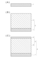
- FIGS. 1 to (C) are schematic views showing the cross-sectional structure of the optical film used in one embodiment of the present invention, respectively.
- 1 is a translucent layer A described later
- 2 is a laminated film
- 3 is a translucent layer B described later
- 3' is a layer or film that serves as a base (base) of the translucent layer B
- 4 is.
- Each hardcourt layer is represented.
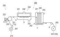
- 100 is a laminated body (laminated film)
- 110 is a support (for example, a base material layer such as a translucent layer B)
- 200 is a manufacturing apparatus
- 201 is a support (for example, a translucent layer B or the like).
- the roll body of the base material layer), 210 is a supply part, 220 is a coating part, 221 is a backup roll, 222 is a coating head, 223 is a decompression chamber, 230 is a drying portion, and 231 is a drying chamber.
- 232 is a drying gas inlet, 233 is a discharge port, 240 is a cooling section, 241 is a cooling chamber, 242 is a cooling air inlet, 243 is a cooling air outlet, and 250 is a winding section.
- 251 represents a roll body of a laminated body (laminated film), and a, b, c, and d represent a transport roll.
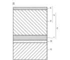
- FIG. 1 is a translucent layer A described later
- 2 is a laminated film
- 3 is a translucent layer B described later
- 3' is a layer or film that serves as a base (base) of the translucent layer B
- 4 is.
- 10 represents a panel unit
- 11 represents an LED module
- 12 represents an adhesive layer.
- 10 represents a panel unit
- 20 represents an independent modular display device.
- XY indicating a range means "X or more and Y or less”. Unless otherwise specified, the operation, physical properties, etc. are measured under the conditions of room temperature (20 to 25 ° C.) / relative humidity of 40 to 50% RH.
- the (co) polymer is a general term including a copolymer and a homopolymer.
- (meth) acrylate is a general term for acrylate and methacrylate.
- compounds containing (meta) such as (meth) acrylic acid are a general term for compounds having "meta” in the name and compounds having no "meta”.
- One aspect of the present invention is a display device having a display surface composed of a plurality of panel units, including particles and a colorant, having a total light transmittance of 10% or more and 30% or less, and including a translucent layer. With respect to the optical film used. According to one aspect of the present invention, in a display device having a display surface composed of a plurality of panel units, it is possible to achieve both an effect of suppressing deterioration of image quality derived from a joint between the panel units and sufficient brightness. Means can be provided.
- a layer containing particles and a colorant and having a total light transmittance of 10% or more and 30% or less is also referred to as a translucent layer A.
- the present inventors presume the mechanism by which the problem is solved by the present invention as follows.
- a display device having a display surface composed of a plurality of panel units
- the external light is reflected by a substrate or the like on which a light emitting element as a light source is mounted, and reflected light is generated. ..
- the reflected light is reflected or refracted on the side surface of the adjacent panel unit and then emitted to the display surface side, so that local scattering of light is visually recognized. It will be. Then, such local scattering of light causes deterioration of the image quality resulting from the joint between the panel units.
- the black encapsulant sheet according to JP-A-2019-204905 Since the black encapsulant sheet according to JP-A-2019-204905 has a function of absorbing visible light, it absorbs and displays the reflected light reflected by a substrate or the like on which a light emitting element as a light source is mounted. The reflected light toward the surface side is reduced, and the scattered light emitted is also reduced. As a result, the deterioration of the image quality caused by the joint between the panel units is suppressed. However, since the black encapsulant sheet according to JP-A-2019-204905 absorbs most of the emitted light emitted from the light emitting element as a light source, the panel unit or the display device provided with such a sheet has a high luminance. It drops significantly.
- the translucent layer A contains a colorant and has a total light transmittance of 10% or more and 30% or less. Since the translucent layer A has a function of absorbing visible light in an appropriate range, it absorbs the reflected light reflected by a substrate or the like on which a light emitting element as a light source is mounted and reflects toward the display surface side. It reduces the light and also reduces the emitted scattered light. In addition, the amount of absorbed light emitted from the light emitting element serving as a light source is also equal to or less than a certain amount. From these facts, sufficient brightness can be obtained in the panel unit or the display device provided with the optical film according to the present invention. Further, in the present invention, the translucent layer A contains particles.
- the particles scatter the reflected light as a whole reflected by the substrate on which the light emitting element that is the light source is mounted, even if the light is scattered at the joint between the panel units, only that part is scattered. Light scattering is less noticeable than when local light scattering occurs. Further, since the emitted light emitted from the light emitting element serving as a light source is also scattered to some extent, the light scattering becomes less noticeable even when the light is scattered at the joint between the panel units.
- the translucent layer A preferably contains a base material.
- the base material imparts self-support to the film and acts to retain the particles in the film.
- the content of the base material is not particularly limited, but from the viewpoint of light transmission, it is preferably more than 50% by mass and more than 80% by mass with respect to the total mass of the translucent layer A. More preferably, it is more than 90% by mass. Further, the content of the base material is preferably less than 100% by mass with respect to the total mass of the translucent layer A from the viewpoint of light absorption and light scattering.
- the base material is not particularly limited and may be an inorganic material or an organic material, but an organic material is preferable.
- the translucent layer A is preferably a translucent resin layer such as a resin film.
- the translucent resin layer represents a translucent layer containing a resin as a base material
- the resin film represents a film containing a resin as a base material.
- the resin as the base material is not particularly limited, and is, for example, an acrylic resin (for example, methyl methacrylate-methyl acrylate copolymer resin, etc.), a polycarbonate resin, a polyolefin resin (for example, a polyethylene resin, a polypropylene resin, etc.), a cycloolefin resin.
- COP polyimide resin
- cellulose resin for example, cellulose triacetate, cellulose diacetate, cellulose acetate propionate, etc.
- polyester resin for example, polyethylene terephthalate (PET), polytrimethylene terephthalate (PTT), polybutylene terephthalate (for example).
- PBT polyethylene naphthalate
- PEN polybutylene naphthalate
- PBN polybutylene naphthalate
- a cycloolefin resin is preferable from the viewpoint of haze value and optical uniformity, and a cycloolefin resin having a polar group is more preferable from the viewpoint of dispersibility of inorganic particles and colorants (particularly pigments).
- polar groups include a carboxy group, a hydroxy group, an alkoxycarbonyl group, an allyloxycarbonyl group, an amino group, an amide group, a cyano group, a group in which these groups are bonded via a linking group such as a methylene group, and a carbonyl group.
- a hydrocarbon group to which a divalent organic group having a polarity such as an ether group, a silyl ether group, a thioether group and an imino group is bonded as a linking group is included.
- a cycloolefin resin having a carboxy group is preferable.
- the polar group is a group capable of forming a salt
- the polar group may form a salt.
- the cycloolefin resin is not particularly limited, but is preferably a (co) polymer of a cycloolefin monomer represented by the following general formula (A).
- Each R of the general formula (A) independently represents a hydrogen atom, a halogen atom, a substituted or unsubstituted hydrocarbon group having 1 to 30 carbon atoms, or a polar group. Further, a and b in the general formula (A) independently indicate integers of 0 or more.
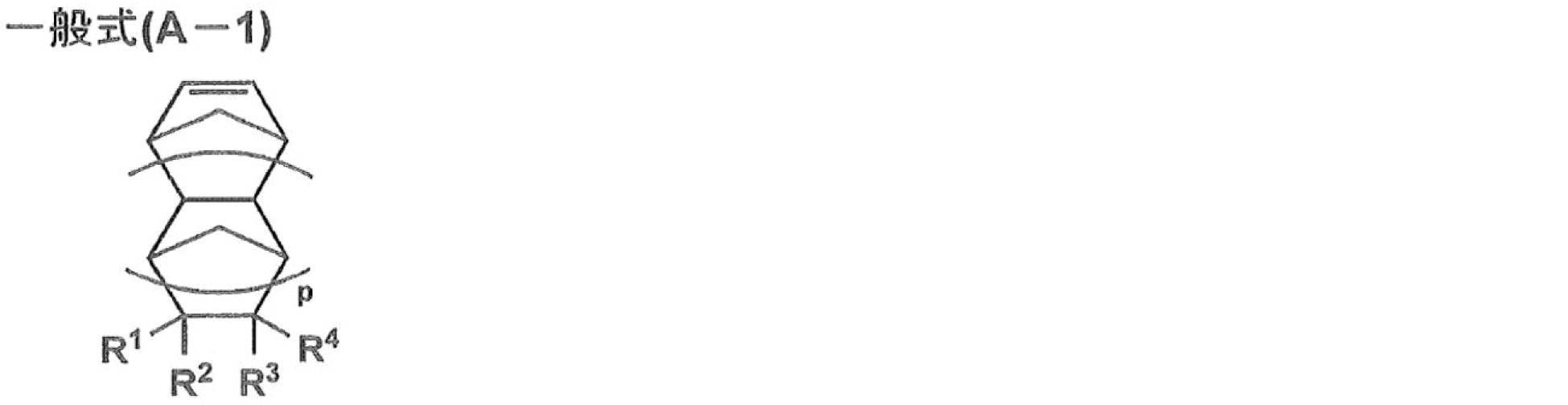
- cycloolefin resin is more preferably a (co) polymer of a cycloolefin monomer represented by the following general formula (A-1) or the following general formula (A-2).
- R 1 to R 4 of the general formula (A-1) independently represent a hydrogen atom, a halogen atom, a substituted or unsubstituted hydrocarbon group having 1 to 30 carbon atoms, or a polar group. However, except when all of R 1 to R 4 are hydrogen atoms, it is assumed that R 1 and R 2 are not hydrogen atoms at the same time, or R 3 and R 4 are hydrogen atoms at the same time.
- the halogen atom is not particularly limited, but is preferably a fluorine atom, a chlorine atom, a bromine atom, or an iodine atom.
- the hydrocarbon group having 1 to 30 carbon atoms is not particularly limited, but is preferably an alkyl group having 1 to 30 carbon atoms.
- the polar group is not particularly limited, but is a carboxy group, a hydroxy group, an alkoxycarbonyl group, an allyloxycarbonyl group, an amino group, an amide group, a cyano group, a group in which these groups are bonded via a linking group such as a methylene group, and the like.
- a divalent organic group having a polarity such as a carbonyl group, an ether group, a silyl ether group, a thioether group or an imino group is bonded as a linking group.
- a carboxy group, a hydroxy group, an alkoxycarbonyl group, or an allyloxycarbonyl group is more preferable.
- an alkoxycarbonyl group or an allyloxycarbonyl group is more preferable.
- At least one of R 1 to R 4 is preferably a polar group from the viewpoint of ensuring the solubility of the cycloolefin resin during solution film formation.
- P in the general formula (A-1) indicates an integer of 0 to 2. From the viewpoint of increasing the heat resistance of the film, p is preferably 1 to 2. This is because when p is 1 to 2, the obtained resin becomes bulky and the glass transition temperature tends to improve.
- R 5 of the general formula (A-2) represents a hydrogen atom, a hydrocarbon group having 1 to 5 carbon atoms, or an alkylsilyl group having an alkyl group having 1 to 5 carbon atoms. Among them, R 5 is preferably a hydrocarbon group having 1 to 3 carbon atoms.
- R 6 in the general formula (A-2) represents a polar group or a halogen atom.
- the polar group is not particularly limited, but is preferably a carboxy group, a hydroxy group, an alkoxycarbonyl group, an allyloxycarbonyl group, an amino group, an amide group, or a cyano group.
- the halogen atom is not particularly limited, but is preferably a fluorine atom, a chlorine atom, a bromine atom, or an iodine atom.
- R 6 is preferably a polar group, a carboxy group, hydroxy group, more preferably an alkoxycarbonyl group or an allyloxycarbonyl group. Further, from the viewpoint of ensuring solubility during solution film formation, an alkoxycarbonyl group or an allyloxycarbonyl group is more preferable.
- p represents an integer of 0 to 2.
- Examples of the copolymerizable monomer copolymerizable with the cycloolefin monomer represented by the general formula (A-1) or the general formula (A-2) include the general formula (A-1) or the general formula (A-2). ) And a ring-open copolymerizable copolymerizable monomer, and an addition copolymerizable copolymer with a cycloolefin monomer represented by the general formula (A-1) or the general formula (A-2). Contains sex monomers.
- Examples of the copolymerizable monomer represented by the general formula (A-1) or the general formula (A-2) and the open-ring copolymerizable monomer include cyclobutene, cyclopentene, cycloheptene, cyclooctene, and dicyclopentadiene. Other cycloolefin monomers such as.
- Examples of copolymerizable monomers that can be additionally copolymerized with the cycloolefin monomer represented by the general formula (A-1) or the general formula (A-2) include unsaturated double bond-containing compounds and vinyl-based cyclic hydrocarbons. Contains compounds, (meth) acrylates. Examples of unsaturated double bond-containing compounds are olefin compounds having 2 to 12 (preferably 2 to 8) carbon atoms, and examples thereof include ethylene, propylene, and butene. Examples of vinyl-based cyclic hydrocarbon compounds include vinyl cyclopentene-based monomers such as 4-vinylcyclopentene and 2-methyl-4-isopropenylcyclopentene.
- Examples of (meth) acrylates include alkyl (meth) acrylates having 1 to 20 carbon atoms such as methyl (meth) acrylate, 2-ethylhexyl (meth) acrylate, cyclohexyl (meth) acrylate.
- the content of the structural units derived from the cycloolefin monomer represented by the general formula (A-1) or the general formula (A-2) is preferably 50 to 50 with respect to the total of the structural units constituting the cycloolefin resin. It is 100 mol%, more preferably 60 to 100 mol%, still more preferably 70 to 100 mol%.
- cycloolefin resin a polymer obtained by homopolymerizing or copolymerizing a cycloolefin monomer represented by the general formula (A-1) or the general formula (A-2) is preferable, and examples thereof include the following. Be done. Among these, (1) to (3) and (5) are preferable, and (3) and (5) are more preferable.
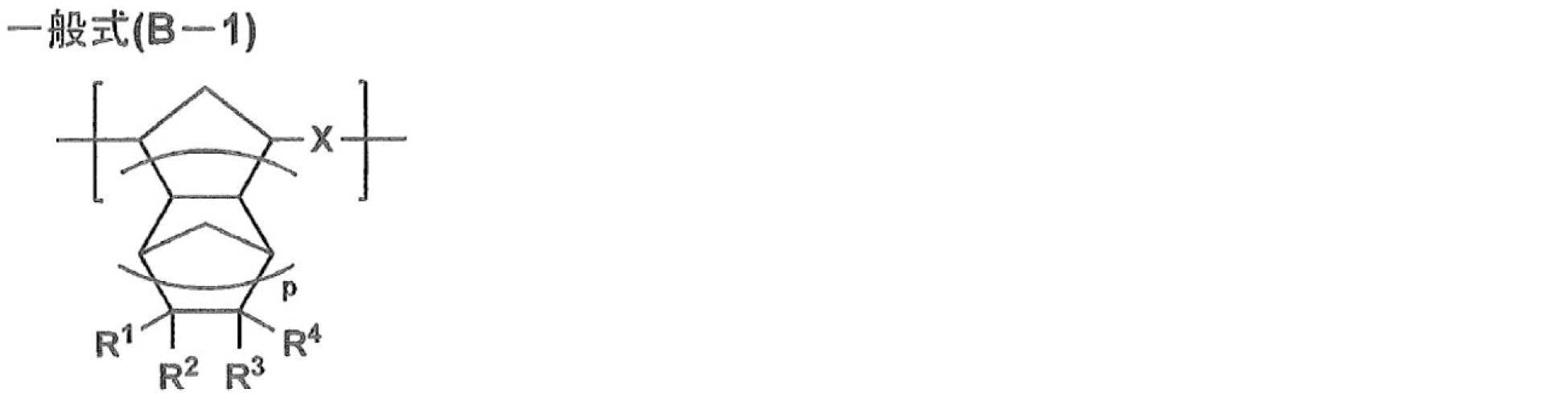
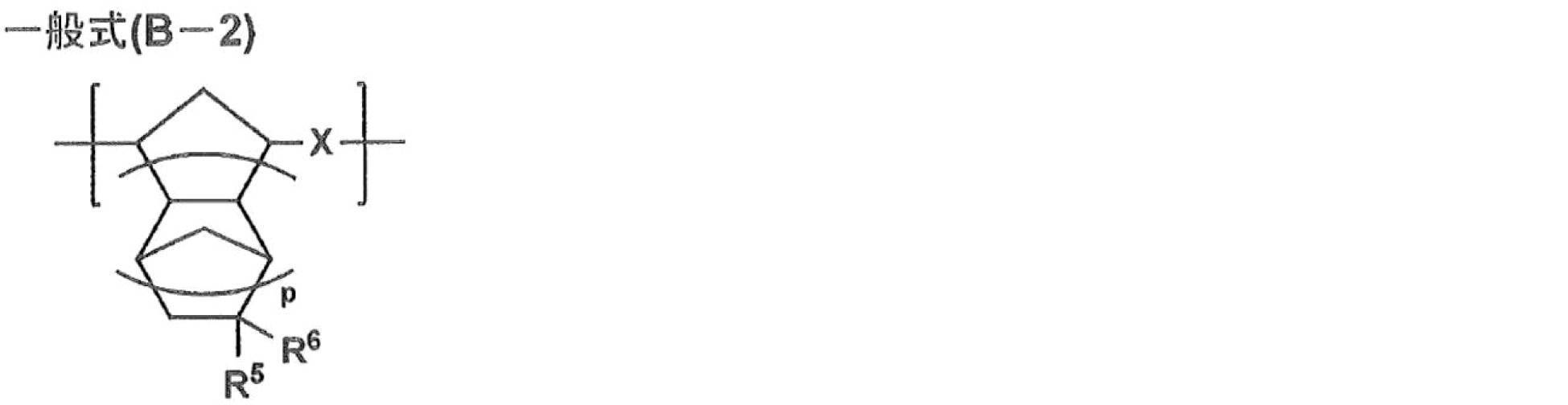
- examples of the cycloolefin resin include those having at least one of a structural unit represented by the following general formula (B-1) and a structural unit represented by the following general formula (B-2). ..
- a copolymer having a structural unit represented by the general formula (B-1) and a structural unit represented by the general formula (B-2) is preferable.
- R 1 ⁇ R 4 and p are each identical to R 1 ⁇ R 4 and p of the general formula (A-1).
- R 5, R 6 and p in the general formula (B-2) are respectively identical to R 5, R 6 and p in the general formula (A-2).
- the intrinsic viscosity [ ⁇ ] inh of the cycloolefin resin is not particularly limited , but is preferably 0.2 to 5 cm 3 / g, more preferably 0.3 to 3 cm 3 / g, and 0.4 to 0.4 to g. It is more preferably 1.5 cm 3 / g.
- the intrinsic viscosity [ ⁇ ] inh of the cycloolefin resin can be measured by JIS K 7637-1: 2002.
- the number average molecular weight (Mn) of the cycloolefin resin is not particularly limited, but is preferably 8000 to 100,000, more preferably 10,000 to 80,000, and even more preferably 12,000 to 50,000.
- the weight average molecular weight (Mw) of the cycloolefin resin is not particularly limited, but is preferably 20,000 to 300,000, more preferably 30,000 to 250,000, and even more preferably 40,000 to 200,000.
- the number average molecular weight (Mn) and the weight average molecular weight (Mw) can be measured in terms of polystyrene by gel permeation chromatography (GPC).
- the glass transition temperature (Tg) of the cycloolefin resin is not particularly limited, but is preferably 110 ° C. or higher, more preferably 110 to 350 ° C., further preferably 120 to 250 ° C., and 120 to 120 ° C. It is particularly preferable that the temperature is 220 ° C.
- Tg is 110 ° C. or higher, deformation is less likely to occur due to secondary processing such as use under high temperature conditions, coating, and printing.
- the Tg is 350 ° C. or lower, the molding process becomes easier and the possibility that the resin is deteriorated by the heat during the molding process becomes lower.
- the Tg of the cycloolefin resin can be measured by JIS K 7121-1987.
- cycloolefin resin a commercially available product or a synthetic product may be used.
- commercially available products include, but are not limited to, Arton (ARTON) (registered trademark, the same shall apply hereinafter) G (for example, Arton G7810), Arton F, Arton R, Arton RX, etc. manufactured by JSR Corporation. Will be.
- the cycloolefin resin can be used alone or in combination of two or more.
- the base material can be used alone or in combination of two or more.
- the translucent layer A according to the embodiment of the present invention contains particles.
- the particles act to scatter the light transmitted through the optical film by being dispersed in the translucent layer A. Therefore, when the translucent layer A does not contain particles, it is insufficient to suppress deterioration of the image quality derived from the joint between the panel units in the display device having the display surface composed of the plurality of panel units.
- the particles do not contain the colorant described later.
- the particles are not particularly limited, and examples thereof include organic particles, inorganic particles, and organic-inorganic composite particles.
- the organic particles are not particularly limited, and examples thereof include polymethylmethacrylate beads, acrylic-styrene copolymer beads, melamine beads, polycarbonate beads, styrene beads, crosslinked polystyrene beads, polyvinyl chloride beads, benzoguanamine-melamine formaldehyde beads and the like. Can be mentioned.
- the inorganic particles are not particularly limited, but are, for example, inorganic oxidation consisting of an oxide containing at least one selected from zirconium, titanium, aluminum, indium, zinc, tin, antimony, cerium, niobium, tungsten, silicon and the like.
- object particles include object particles. Specifically, ZrO 2, ZrSiO 4, TiO 2, BaTiO 3, SrTiO 3, Al 2 O 3, zeolites, In 2 O 3, ITO ( Indium Tin Oxide), ZnO, SnO 2, Sb 2 O 3, CeO 2 , Nb 2 O 5 , WO 3 , silica (SiO 2 ) and the like can be mentioned.
- inorganic particles are preferable, inorganic oxide particles are more preferable, oxides containing silicon are further preferable, and silica (SiO 2 ) is particularly preferable.
- the particles may have a multi-layer structure including a core-shell structure.
- specific materials for surface treatment include dissimilar inorganic oxides such as silicon oxide and zirconium oxide, metal hydroxides such as aluminum hydroxide, and organic acids such as organosiloxane and stearic acid. Be done.
- these surface treatment materials one type may be used alone, or a plurality of types may be used in combination. Among them, from the viewpoint of the stability of the dispersion liquid, at least one of a dissimilar inorganic oxide and a metal hydroxide is preferable as a surface treatment material, and a metal hydroxide is more preferable.
- the average secondary particle diameter of the particles is not particularly limited, but is preferably 50 nm or more, more preferably 100 nm or more, and further preferably 150 nm or more. Within these ranges, the effect of suppressing deterioration of image quality derived from the joints between the panel units is further improved.
- the average secondary particle diameter of the particles is preferably 1000 nm or less, more preferably 500 nm or less, and even more preferably 300 nm or less. Within these ranges, the effect of suppressing deterioration of image quality, which makes the image unclear as a whole, is further enhanced.
- the average secondary particle size of the particles can be obtained by directly measuring the size of the secondary particles from the electron micrograph of the layer. Specifically, the particle image was measured by a transmission electron micrograph (TEM) (H-7650 manufactured by Hitachi High-Tech Co., Ltd.), and the average value of the equivalent diameters of 100 secondary particles selected at random. Is obtained, and this value is taken as the average secondary particle diameter.
- TEM transmission electron micrograph
- the particles a commercially available product or a synthetic product may be used.
- the commercially available product is not particularly limited, and examples thereof include R972V manufactured by Nippon Aerosil Co., Ltd.
- the particles can be used alone or in combination of two or more.
- the content of the particles in the translucent layer A is not particularly limited, but is preferably 0.01 part by mass or more, and more preferably 0.05 part by mass or more with respect to 100 parts by mass of the base material. It is more preferably 0.1 part by mass or more, and particularly preferably 0.3 part by mass or more. Within these ranges, the effect of suppressing deterioration of image quality derived from the joints between the panel units is further improved.
- the content of the particles in the translucent layer A is not particularly limited, but is preferably 10 parts by mass or less, more preferably 5 parts by mass or less, based on 100 parts by mass of the base material. It is more preferably 1 part by mass or less. Within these ranges, the effect of suppressing deterioration of image quality, which makes the image unclear as a whole, is further enhanced.
- the translucent layer A according to the embodiment of the present invention contains a colorant.
- the colorant colors the translucent layer A and acts to control the total light transmittance of the optical film. Therefore, when the translucent layer A does not contain a colorant, in a display device having a display surface composed of a plurality of panel units, it is insufficient to suppress deterioration of image quality derived from joints between the panel units. ..
- the colorant is not particularly limited, and examples thereof include dyes and pigments.
- the pigment is not particularly limited, and examples thereof include organic pigments, inorganic pigments, minerals and the like having the following numbers listed in the color index.
- the black pigment is not particularly limited, and examples thereof include carbon black, magnetic materials, and iron / titanium composite oxide black.
- the carbon black is not particularly limited, and examples thereof include channel black, furnace black, acetylene black, thermal black, and lamp black.
- the magnetic material is not particularly limited, and examples thereof include ferrite and magnetite.
- the red or magenta pigment is not particularly limited, but for example, C.I. I. Pigment Red 3, 5, 19, 22, 31, 38, 43, 48: 1, 48: 2, 48: 3, 48: 4, 48: 5, 49: 1, 53: 1, 57: 1, 57: 2, 58: 4, 63: 1, 81, 81: 1, 81: 2, 81: 3, 81: 4, 88, 104, 108, 112, 122, 123, 144, 146, 149, 166, 168, 169, 170, 177, 178, 179, 184, 185, 208, 216, 226, 257, Pigment Violet 3, 19, 23, 29, 30, 37, 50, 88, Pigment Orange 13, 16, 20, 36, Ruby (chromium-containing corundum), garnet (garnet), spinel (spine) and the like can be mentioned.
- the blue or cyan pigment is not particularly limited, but for example, C.I. I. Pigment Blue 1, 15, 15: 1, 15: 2, 15: 3, 15: 4, 15: 6, 16, 17-1, 22, 27, 28, 29, 36, 60, blue sapphire (iron, titanium) Containing corundum) and the like.
- the green pigment is not particularly limited, but for example, C.I. I. Pigment Green 7, 26, 36, 50 and the like.
- the yellow pigment is not particularly limited, but for example, C.I. I. Pigment Yellow 1, 3, 12, 13, 14, 17, 34, 35, 37, 55, 74, 81, 83, 93, 94, 95, 97, 108, 109, 110, 137, 138, 139, 153, 154, 155, 157, 166, 167, 168, 180, 185, 193, yellow sapphire (nickel-containing corundum) and the like can be mentioned.
- the dye is not particularly limited, and examples thereof include conventionally known dyes, for example, those described in paragraphs "0057” to "0060” of International Publication No. 2015/111351.
- the colorant when the base material is a resin, a pigment is preferable from the viewpoint of having good dispersion stability with respect to the resin and having excellent weather resistance. That is, it is more preferable that the translucent layer A according to the embodiment of the present invention further contains a pigment and a resin in addition to the above particles. Further, among the pigments, a black pigment is more preferable, and a carbon black is further preferable, from the viewpoint that the change in the color of the image is more suppressed and the effect of the present invention is more preferably exhibited.
- the average secondary particle size of the pigment is not particularly limited, but is preferably 0.1 ⁇ m or more, and more preferably 0.2 ⁇ m or more. Within these ranges, the slidability becomes better and it becomes more difficult to aggregate, so that the unevenness of the total light transmittance of the film is further reduced.
- the average secondary particle size of the pigment is not particularly limited, but is preferably less than 3 ⁇ m, more preferably less than 2.6 ⁇ m. Within these ranges, dispersion spots in the film are less likely to occur, unevenness in the total light transmittance of the film is further reduced, and the haze value is also lowered.
- the average secondary particle size of the pigment can be obtained by directly measuring the size of the secondary particles from the electron micrograph of the layer. Specifically, the particle image was measured by a transmission electron micrograph (TEM) (H-7650 manufactured by Hitachi High-Tech Co., Ltd.), and the average value of the equivalent diameters of 100 secondary particles selected at random. Is obtained, and this value is taken as the average secondary particle diameter.
- TEM transmission electron micrograph
- the colorant a commercially available product or a synthetic product may be used.
- the commercially available product is not particularly limited, and examples thereof include # 950 manufactured by Mitsubishi Chemical Corporation.
- the colorant can be used alone or in combination of two or more.
- the content of the colorant in the translucent layer A is not particularly limited, but is preferably 0.01 part by mass or more, and preferably 0.05 part by mass or more with respect to 100 parts by mass of the base material. It is more preferably 0.1 part by mass or more, and further preferably 0.1 part by mass or more. Within these ranges, the effect of suppressing deterioration of image quality derived from the joints between the panel units is further improved.
- the content of the colorant in the translucent layer A is not particularly limited, but is preferably 10 parts by mass or less and more preferably 5 parts by mass or less with respect to 100 parts by mass of the base material. It is more preferably 1 part by mass or less, and particularly preferably 0.6 part by mass or less. Within these ranges, the brightness is further improved.
- the translucent layer A according to the embodiment of the present invention may further contain components other than the components described above as long as the effects of the present invention are not impaired.
- the other components are not particularly limited, and examples thereof include known components used in the field of optical films and known fields of functional layers for optical applications. Specific examples thereof include, but are not limited to, a phase difference adjuster, a wavelength dispersion adjuster, a plasticizer, an ultraviolet absorber, an antioxidant, a hydrogen-bonding solvent, and an ionic surfactant. ..
- the total light transmittance of the translucent layer A according to the embodiment of the present invention is 10% or more and 30% or less. If the total light transmittance is less than 10%, the brightness becomes insufficient in a display device having a display surface composed of a plurality of panel units. Further, when the total light transmittance is more than 30%, the deterioration of the image quality derived from the joint between the panel units in the display device having the display surface composed of the plurality of panel units is insufficiently suppressed.
- the total light transmittance of the translucent layer A shall be 15% or more and 25% or less from the viewpoint of improving both the brightness and the effect of suppressing the deterioration of the image quality derived from the joint between the multiple panel units. Is preferable.
- the total light transmittance can be measured using a haze meter (NDH4000, manufactured by Nippon Denshoku Kogyo Co., Ltd.) according to JIS K 7631-1: 1997 (test method for total light transmittance of plastic-transparent material). ..
- the translucent layer A may be surface-modified.
- the method of the surface modification treatment is not particularly limited, and examples thereof include a corona discharge treatment, a flame treatment, an oxidation treatment, and a plasma treatment.
- the film thickness of the translucent layer A is not particularly limited, but is preferably 1 ⁇ m or more, more preferably 3 ⁇ m or more, further preferably 5 ⁇ m or more, and particularly preferably 8 ⁇ m or more. Within these ranges, the effect of suppressing deterioration of image quality derived from the joints between the panel units in a display device having a display surface composed of a plurality of panel units is further improved.
- the film thickness of the translucent layer A is preferably less than 50 ⁇ m, more preferably less than 20 ⁇ m, further preferably 15 ⁇ m or less, and particularly preferably 10 ⁇ m or less. Within these ranges, the brightness is further improved in a display device having a display surface composed of a plurality of panel units.
- the translucent layer A may be used as a single-layer film composed of only the layer, or may form a part of an optical film, but is one of the optical films. It is preferable to form a part.
- the optical film according to the embodiment of the present invention further includes a base material layer which is another layer.
- the base material layer can contribute to the protection of the translucent layer A, the impartation of mechanical properties to the optical film, the improvement of the handling suitability of the optical film, and the like.
- the base material layer may be a release film that is peeled off during use.
- the base material layer may have a functional layer on one side or both sides, as will be described later.
- the base material layer is not particularly limited, but is preferably a translucent layer B.
- the translucent layer B is not particularly limited as long as it can transmit at least a part of the incident light.
- the total light transmittance of the translucent layer B is preferably 50% or more, more preferably 60% or more, further preferably 80% or more, and particularly preferably 90% or more. .. Within these ranges, when an optical film including the above-mentioned translucent layer A and another translucent layer B is used, a display surface composed of a plurality of panel units is used. The brightness is further improved in the display device having the above.
- the total light transmittance of the translucent layer B is not particularly limited, but is more preferably 95% or less, further preferably 93% or less, and particularly preferably 91% or less. Within these ranges, it becomes easier to satisfy the relationship between the haze values of the translucent layer A and the translucent layer B, which will be described later.
- the total light transmittance can be measured using a haze meter (NDH4000, manufactured by Nippon Denshoku Kogyo Co., Ltd.) according to JIS K 7631-1: 1997 (test method for total light transmittance of plastic-transparent material). ..
- the base material layer is a translucent layer B which is another translucent layer, and the translucent layer B is arranged on the translucent layer A.
- the translucent layer A and the translucent layer B are the translucent layer A when the haze of the laminate of one translucent layer A and one translucent layer B is measured.
- the value Hz (AB) (%) when light is incident from the side and the value Hz (BA) (%) when light is incident from the translucent layer B side are Hz ( It is preferable to satisfy the relationship of AB) ⁇ Hz (BA).
- the reason for this is that the light transmitted through the optical film is transmitted by arranging the optical film with the transparent layer A facing the light emitting module side and the transparent layer B facing the display surface side (that is, the visual recognition side in the display device). It is presumed that this is because the light is scattered more, but the correctness does not affect the technical scope of the present invention.
- the haze value can be measured using a haze meter (NDH4000, manufactured by Nippon Denshoku Kogyo Co., Ltd.) according to JIS K 7136: 2000.
- the translucent layer B is arranged on the translucent layer A
- the translucent layer A is in contact with the translucent layer A on the surface of the translucent layer A.
- the translucent layer B is arranged on the translucent layer A between the translucent layer A and the translucent layer B via another member. It means that the configuration to be used is also included.
- the translucent layer B is arranged on the surface of the translucent layer A so as to be in contact with the translucent layer A.
- the number of base material layers may be one or two or more, but one is preferable. Regardless of whether the optical film has only one base material layer or two or more base layers, it is preferable that the translucent layer A constitutes one outermost surface of the optical film.
- the base material layer (when the base material layer has a functional layer described later, a layer or a film that serves as a base (that is, a base) of the base material layer) preferably contains a base material.
- a base material layer such as the translucent layer B described later
- the layer or film on which the functional layer is formed is referred to as "mother”. Or "basic”.
- the content of the base material is not particularly limited, but from the viewpoint of light transmission, a base material layer (when the base material layer has a functional layer described later, a layer or film serving as a base (base) of the base material layer). Etc.), it is preferably more than 50% by mass, more preferably more than 80% by mass, and further preferably more than 90% by mass with respect to the total mass. Further, the content of the base material is a layer that becomes a base material (base) of the base material layer (when the base material layer has a functional layer described later, the base material layer is a base material) from the viewpoint of light absorption and light scattering property. Alternatively, it is preferably less than 100% by mass with respect to the total mass of the film or the like).
- the base material of the base material (when the base material has a functional layer described later, a layer or a film serving as a base (that is, a base) of the base layer) is not particularly limited, and the above-mentioned translucency is not particularly limited.
- the base material layer (when the base material layer has a functional layer described later, a layer or a film serving as a base (that is, a base) of the base material layer) is a resin layer such as a resin film (for example, translucent). Resin layer) is preferable.
- the resin film represents a film containing a resin as a base material. Examples of the resin as the base material include the same as those mentioned as the resin as the base material of the translucent layer A described above. Among these, from the viewpoint of haze value, polyester resin is preferable, and polyethylene terephthalate is more preferable.
- the base material can be used alone or in combination of two or more.
- the base material layer (when the base material layer has a functional layer described later, a layer or a film that serves as a base (base) of the base material layer) is other than the base material described above as long as the effect of the present invention is not impaired. It may further contain other components.
- the other components are not particularly limited, and examples thereof include particles and colorants described in the above-mentioned translucent layer A. Further, for example, each component used in a known optical film field and a known functional layer field for optical applications can be mentioned. Specific examples thereof include particles, colorants, retardation adjusters, wavelength dispersion adjusters, plasticizers, ultraviolet absorbers, antioxidants, hydrogen-bonding solvents, ionic surfactants, etc., but are limited thereto. It is not something that is done.
- the base material layer may be surface-modified.
- the method of the surface modification treatment is not particularly limited, and examples thereof include a corona discharge treatment, a flame treatment, an oxidation treatment, and a plasma treatment.
- the base material layer may have a functional layer on one side or both sides of a layer or a film that serves as a base (base) thereof. More specifically, the base material layer is on the translucent layer A side (that is, between the translucent layer A and the layer or film that is the base (base) of the base material layer), or is translucent. It may have a functional layer on the opposite side of the sex layer A.
- the base material layer has a functional layer
- it is treated as a base material layer including the functional layer.
- the translucent layer B has a functional layer
- it is treated as the translucent layer B including the functional layer.
- the functional layer of the base material layer is not particularly limited, and examples thereof include functional layers used in optical applications. Specific examples thereof include a release layer, an easy-adhesion layer, an antistatic layer, a hard coat layer, an antireflection layer, an antiglare layer, a barrier layer, a cushioning layer, an easy-slip layer, and the like, but are limited thereto. It's not a thing. Among these, the easy-adhesion layer or the hard coat layer is preferable, and the easy-adhesion layer is more preferable.
- the easy-adhesion layer is not particularly limited, and a known easy-adhesion layer can be appropriately used.
- the easy-adhesion layer only on one surface of the layer or film which is the base (base) of the translucent layer B, or on both surfaces. .. Among these, it is more preferable to provide an easy-adhesion layer on the surface of the translucent layer A side, such as at least a layer or a film that serves as a base (base) of the translucent layer B.
- the hard coat layer is not particularly limited, and examples thereof include a cured layer containing a resin containing an alicyclic hydrocarbon and fine particles coated with a polymer silane coupling agent. When the hard coat layer is provided, it is preferable to further provide a cushioning layer between the hard coat layer and the film.
- the buffer layer is not particularly limited, and examples thereof include a layer containing a resin different from the resin contained in the hard coat layer and fine particles coated with a polymer silane coupling agent.
- the hard coat layer is preferably provided on only one surface side such as a layer or film serving as a base (base) of the translucent layer B, or on both surface sides. ..
- the base material layer may have only one functional layer on one side or both sides, or may have two or more laminated layers.
- the film thickness of the functional layer of the base material layer is not particularly limited, but is preferably less than 10 ⁇ m, more preferably less than 8 ⁇ m, further preferably less than 5 ⁇ m, and particularly preferably less than 3 ⁇ m. (Lower limit over 0 ⁇ m).
- the film thickness of the base material layer is not particularly limited, but is preferably 10 ⁇ m or more, more preferably 20 ⁇ m or more, further preferably 30 ⁇ m or more, and particularly preferably 50 ⁇ m or more. Within these ranges, the protective effect of the translucent layer A, the effect of imparting mechanical properties to the optical film, the handling suitability of the optical film, and the like are further improved. Further, when the base material layer is the translucent layer B, in a display device having a display surface composed of a plurality of panel units, the suppression of deterioration of image quality derived from the joints between the panel units is further improved.
- the film thickness of the base material layer is preferably 500 ⁇ m or less, more preferably 200 ⁇ m or less, further preferably 100 ⁇ m or less, and particularly preferably 80 ⁇ m or less. Within these ranges, when the base material layer is a translucent layer, the brightness is further improved in a display device having a display surface composed of a plurality of panel units.
- the film thickness of the translucent layer A is preferably thinner than the film thickness of the base material layer.
- a commercially available product may be used as the base material layer.
- the commercial product is not particularly limited, but when the base material layer is the translucent layer B, for example, Zeonoa (registered trademark) ZF16 manufactured by Nippon Zeon Corporation and Cosmo Shine (registered trademark) manufactured by Toyobo Corporation. ) A4300 and the like can be mentioned.
- the optical film according to the embodiment of the present invention may further have a functional layer other than the translucent layer A and the base material layer, that is, a functional layer other than the above-mentioned functional layer of the base material layer. ..
- the optical film according to the embodiment of the present invention may further have another functional layer on one side or both sides of the translucent layer A, if necessary.
- the details of the other functional layers are also the same as the description of the functional layers of the base material layer described above.
- the translucent layer A and the translucent layer A are provided on one side or both sides.
- the total light transmittance of the laminated body with the other functional layer obtained is preferably 10% or more and 30% or less, and more preferably 15% or more and 25% or less.
- the total light transmittance can be measured using a haze meter (NDH4000, manufactured by Nippon Denshoku Kogyo Co., Ltd.) according to JIS K 7631-1: 1997 (test method for total light transmittance of plastic-transparent material). ..
- one translucent layer A and one translucent layer B are used.
- the value Hz (BA) (%) when light is incident from the translucent layer B side have a relationship of Hz (AB) ⁇ Hz (BA). It is preferable to meet.
- the haze value can be measured using a haze meter (NDH4000, manufactured by Nippon Denshoku Kogyo Co., Ltd.) according to JIS K 7136: 2000.
- FIG. 1A represents a single-layer film composed of only the translucent layer A1.
- FIG. 1B represents a laminated film 2 in which a translucent layer A 1 and a translucent layer B 3 are laminated.
- one outermost surface is formed by the translucent layer A1 and the other outermost surface is formed by the translucent layer B3.
- the translucent layer B 3 is arranged so as to be in contact with the translucent layer A 1.
- the translucent layer B has an easily adhesive layer (not shown), and the easily adhesive layer (not shown) is in contact with the translucent layer A1 on the surface of the translucent layer A1.
- FIG. 1C shows a laminated film 2 in which a translucent layer A 1 and a translucent layer B 3 are laminated, and further, the translucent layer B 3 is a translucent layer A.
- one outermost surface is composed of the translucent layer A1, and the translucent layer B 3 is in contact with the translucent layer A 1 on the surface of the translucent layer A 1.
- the translucent layer B has an easily adhesive layer (not shown), and the easily adhesive layer (not shown) is in contact with the translucent layer A1 on the surface of the translucent layer A1.
- the translucent layer B 3 having the above is arranged. Further, for example, it is also preferable that the hard coat layer 4 is formed on the easy-adhesion layer (not shown) of the translucent layer B3 having the easy-adhesion layer (not shown).
- 3' represents the layer or film which becomes the base (base) of the translucent layer B3.
- the method for producing an optical film according to an embodiment of the present invention is not particularly limited, and a known method for producing an optical film can be used.
- a coating method, a solution casting method, a melt casting method, a gas phase film forming method and the like can be mentioned.
- a method having a forming step and a drying step of 3) removing the solvent from the coating film of the applied coating liquid for forming the translucent layer A to form the translucent layer A is preferable.
- the support is a base material layer (for example, a translucent layer B)
- a laminated film including the translucent layer A and the base material layer can be produced by the production method. can.
- Coating liquid preparation step In this step, the coating liquid for forming the translucent layer A containing the particles described in the translucent layer A above, the colorant described in the translucent layer A above, and the solvent. To prepare.
- the coating liquid for forming the translucent layer A may further contain a base material (for example, a resin) or other components, if necessary.
- a particle dispersion liquid and a colorant dispersion liquid or a colorant solution are prepared, and these dispersion liquids or solutions, a solvent, and if necessary, a base material are used. It is preferable to prepare by mixing with other components as needed.
- the preparation of the particle dispersion liquid and the colorant dispersion liquid or the colorant solution are not particularly limited, but it is preferable to use those listed as examples of the solvent used in the following coating liquid for forming the translucent layer A. .. Further, in the preparation of the particle dispersion liquid and the colorant dispersion liquid or the colorant solution, it is preferable to perform filtration. A known filtration device can be appropriately used for filtration.
- the solvent used for the coating liquid for forming the translucent layer A is not particularly limited, but for example, chlorine-based solvents such as chloroform and dichloromethane, methanol, ethanol, propanol, n-butanol, 2-butanol, tert-butanol, and cyclo Alcohols such as hexanol, ketones such as methyl ethyl ketone, methyl isobutyl ketone and acetone, esters such as ethyl acetate, methyl acetate, ethyl lactate, isopropyl acetate, amyl acetate and ethyl butyrate, glycol ethers (propylene glycol mono (C1 ⁇ ) C4) Alkyl ether (specifically, propylene glycol monomethyl ether (PGME), propylene glycol monoethyl ether, propylene glycol mono-n-propyl ether, propylene glycol monoisopropyl
- a chlorine-based solvent from the viewpoint of easily dissolving the base material, having a low boiling point, and easily increasing the drying rate and productivity, it is preferable to contain a chlorine-based solvent, alcohols, and ketones, and it is preferable to contain a chlorine-based solvent. More preferred.
- a chlorine-based solvent preferably a chlorine-based solvent, alcohols, and ketones.
- Dichloromethane is preferable as the chlorine-based solvent.
- alcohols methanol or ethanol is preferable, and ethanol is more preferable.
- ketones methyl ethyl ketone or acetone is preferable, and methyl ethyl ketone is more preferable. That is, it is particularly preferable to contain dichloromethane and at least one of ethanol and methyl ethyl ketone.
- the ratio of the chlorine-based solvent is moderately high, it is easy to improve the drying property and productivity.
- the concentration of the base material in the coating liquid for forming the translucent layer A is preferably 1 to 20% by mass from the viewpoint of making it easy to adjust the viscosity within an appropriate range. Further, from the viewpoint of reducing the amount of shrinkage of the coating film during drying, the concentration of the base material in the coating liquid for forming the translucent layer A is more preferably more than 5% by mass and 20% by mass or less. It is more preferably more than mass% and 15% by mass or less.
- the mixing conditions are not particularly limited in the preparation of various dispersions or solutions such as the coating liquid for forming the translucent layer A, the preparation of the particle dispersion, the colorant dispersion or the colorant solution.
- As the mixing temperature it may be mixed at room temperature, or it may be mixed while heating in order to improve the solubility.
- the mixing time is not particularly limited, but when the base material is mixed, it is preferably a time during which the base material is completely dissolved.
- a known mixing device can be appropriately used for mixing.
- the viscosity of the coating liquid for forming the translucent layer A is not particularly limited, but is preferably 5 to 5000 mPa ⁇ s.
- the viscosity of the coating liquid for forming the translucent layer A is 5 mPa ⁇ s or more, it becomes easier to form a layer having an appropriate thickness.
- the viscosity of the coating liquid for forming the translucent layer A is 5000 mPa ⁇ s or less, the occurrence of thickness unevenness can be further suppressed due to the increase in the viscosity of the solution.
- the viscosity of the coating liquid for forming the translucent layer A is more preferably 100 to 1000 mPa ⁇ s.
- the viscosity can be measured with an E-type viscometer at 25 ° C.
- Coating film forming step In this step, the obtained coating liquid for forming the translucent layer A is applied to the surface of the support. Specifically, the obtained coating liquid for forming the translucent layer A is applied to the surface of the support.
- the coating method of the coating liquid for forming the translucent layer A is not particularly limited, and a known coating method can be used.
- a back coat method, a gravure coat method, a spin coat method, a wire bar coat method, a roll coat method and the like can be mentioned.
- the back coat method is preferable from the viewpoint of being able to form a thin and uniform thickness coating film.
- the base material layer When manufacturing a laminated film, it is preferable to use a base material layer as a support as described above. The details of the base material layer are as described above.
- the base material layer When a base material layer is used as the support, the base material layer has a functional layer (for example, an easily adhesive layer), and is used for forming the translucent layer A on the surface on which the functional layer is formed. It is also preferable to apply a coating liquid.
- Drying step In this step, the solvent is removed from the coating film of the coating liquid for forming the translucent layer A applied to the support to form the translucent layer A. Specifically, the coating film of the coating liquid for forming the translucent layer A applied to the support is dried.
- the method of applying the coating liquid for forming the translucent layer A is not particularly limited, and a known drying method can be used.
- a method by blowing air or heating can be mentioned.
- the method by blowing air is preferable from the viewpoint of facilitating the suppression of curl and the like.
- the drying speed of the coating film is not particularly limited, but is preferably 0.0015 to 0.05 kg / hr ⁇ m 2 , and more preferably 0.002 to 0.05 kg / hr ⁇ m 2 .
- the drying rate is expressed as the mass of the solvent that evaporates per unit time and unit area.
- the drying rate can usually be adjusted by the drying temperature.
- the drying temperature is not particularly limited, but is preferably (Tb-50) to (Tb + 50) ° C., for example, 50 to 200 ° C. with respect to the boiling point Tb of the solvent used.
- the translucent layer A can be used as it is as a laminated film without peeling from the base material layer.
- the base material layer is a translucent layer B composed of only the above-mentioned base layer or film, or a translucent layer B having a functional layer (for example, an easily adhesive layer).
- the translucent layer A can be used as it is as an optical film without being peeled off.
- the optical film according to the embodiment of the present invention may be strip-shaped. Therefore, the method for manufacturing an optical film may further include 4) a winding step of winding a strip-shaped optical film into a roll to form a roll.
- the width of the obtained strip-shaped translucent layer A, a laminate of the translucent layer A and the base material layer, or a layer obtained by forming another functional layer on these, if necessary, is used. It is wound into a roll in a direction orthogonal to the direction to form a roll body.
- the length of the strip-shaped optical film is not particularly limited, but is preferably about 100 to 10,000 m, for example.
- the width of the strip-shaped optical film is preferably 1 m or more, more preferably 1.3 to 4 m.
- optical film according to the embodiment of the present invention is not particularly limited, but can be manufactured by, for example, the manufacturing apparatus shown in FIG.
- FIG. 2 is a schematic view of a manufacturing apparatus 200 for manufacturing an optical film according to an embodiment of the present invention.
- the manufacturing apparatus 200 includes a supply unit 210, a coating unit 220, a drying unit 230, a cooling unit 240, and a winding unit 250.
- Reference numerals a to d indicate transport rolls for transporting the support 110.
- the supply unit 210 has a feeding device (not shown) for feeding out the roll body 201 of the strip-shaped support 110 wound around the winding core.
- the coating unit 220 is a coating device, and includes a backup roll 221 that holds the support 110 and a coating head 222 that applies the coating liquid for forming the translucent layer A to the support 110 held by the backup roll 221. It has a decompression chamber 223 provided on the upstream side of the coating head 222.
- the flow rate of the coating liquid for forming the translucent layer A discharged from the coating head 222 can be adjusted by a pump (not shown).
- the flow rate of the coating liquid for forming the translucent layer A discharged from the coating head 222 is set to an amount capable of stably forming a coating layer having a predetermined film thickness when continuously coated under the conditions of the coating head 222 adjusted in advance. Has been done.
- the decompression chamber 223 is a mechanism for stabilizing a bead (pool of coating liquid) formed between the coating liquid for forming the translucent layer A from the coating head 222 and the support 110 at the time of coating, and the pressure reducing chamber 223 is depressurized. The degree can be adjusted.
- the decompression chamber 223 is connected to a decompression blower (not shown) so that the inside is decompressed.
- the decompression chamber 223 is in a state where there is no air leakage, and the gap with the backup roll is narrowly adjusted so that a stable bead of the coating liquid can be formed.
- the drying unit 230 is a drying device that dries the coating film applied to the surface of the support 110, and has a drying chamber 231, a drying gas introduction port 232, and a discharge port 233.
- the temperature and air volume of the dry air are appropriately determined depending on the type of the coating film and the type of the support 110.
- the amount of residual solvent in the coating film after drying can be adjusted.
- the amount of residual solvent in the coating film after drying can be measured by comparing the unit mass of the coating film after drying with the mass after the coating film is sufficiently dried.
- the cooling unit 240 cools the temperature of the support 110 having the coating film (translucent layer A (not shown)) obtained by drying in the drying unit 230, and adjusts the temperature to an appropriate temperature.
- the cooling unit 240 has a cooling chamber 241, a cooling air inlet 242, and a cooling air outlet 243.
- the temperature and air volume of the cooling air can be appropriately determined depending on the type of the coating film and the type of the support 110. Further, even if the cooling unit 240 is not provided, the cooling unit 240 may not be provided if the cooling temperature is appropriate.
- the winding unit 250 is a winding device (not shown) for winding the support 110 (laminated body 100) on which the translucent layer A (not shown) is formed to obtain the roll body 251.
- a base material layer for example, a translucent layer B
- the laminated body 100 of the translucent layer A and the support becomes a laminated film.
- the optical film according to an embodiment of the present invention is used for a display device having a display surface composed of a plurality of panel units.
- the optical film according to the embodiment of the present invention is not particularly limited, but can be preferably applied to, for example, those listed in the following detailed description of the panel unit and the display device.
- the panel unit to which the above optical film is applied and the display device including the panel unit are not particularly limited, but are preferably a self-luminous panel unit and a display device having a display surface composed of the self-luminous panel unit.
- the above optical film is used for a display device having a display surface composed of a panel unit having a light emitting module. That is, another aspect of the present invention is a plurality of panel units having a light emitting module and the above-mentioned optical film arranged on the display surface side (that is, the visual recognition side in the display device) with respect to the light emitting module. It can also be said that it relates to a panel unit used in a display device having a configured display surface.
- the above-mentioned optical film when the above-mentioned optical film includes the above-mentioned translucent layer A and the above-mentioned base material layer (preferably, the above-mentioned translucent layer B), the above-mentioned translucent layer A is used.
- the above-mentioned base material layer preferably, the translucent layer B
- the above-mentioned optical film is used for a display device having a display surface composed of a panel unit having a light emitting module. Is more preferable.
- another aspect of the present invention has a light emitting module and the above-mentioned optical film arranged on the display surface side of the light-emitting module, and is closer to the display surface side than the above-mentioned translucent layer A.
- the present invention relates to a panel unit used in a display device having a display surface composed of a plurality of panel units on which the above-mentioned base material layer (preferably a translucent layer B) is arranged.
- the translucent layer A constitutes one outermost surface of the optical film, and the surface of the optical film on the translucent layer A side and the light emitting module are arranged so as to face each other.
- the panel unit is not particularly limited, and for example, a panel unit having a known light emitting module can be used.
- a panel unit having a known light emitting module can be used.
- the light emitting module can be displayed directly on the display screen by blinking.
- the light emitting element included in the light emitting module is more preferably an LED element. That is, it is more preferable that the light emitting module is an LED module in which the light emitting element is an LED element.
- the panel unit includes the light emitting module and the above optical film
- the light emitting module and the above optical film are bonded to each other with an adhesive.
- the base material layer preferably the translucent layer B
- the translucent layer A constitutes one outermost surface of the optical film, and the surface of the optical film on the translucent layer A side and the light emitting module are bonded so as to face each other.
- a known adhesive can be used without particular limitation, and examples thereof include a pressure-sensitive adhesive, a heat-curable adhesive, and a photocurable adhesive.
- a pressure-sensitive adhesive is preferable.
- the pressure-sensitive adhesive is not particularly limited, and is, for example, an acrylic pressure-sensitive adhesive, a rubber-based pressure-sensitive adhesive, a silicone-based pressure-sensitive adhesive, a urethane-based pressure-sensitive adhesive, a polyacrylamide-based pressure-sensitive adhesive, or the like. Can be mentioned.
- the panel unit will have a light emitting module, the above optical film, and an adhesive layer arranged between them.
- the panel unit includes the light emitting module and the above optical film
- the light emitting module, the above optical film, and other members adopted as necessary are integrated by heat pressing. It may be pasted together.
- the base material layer preferably the translucent layer B
- the translucent layer A constitutes one outermost surface of the optical film
- the surface of the optical film on the translucent layer A side and the light emitting module are bonded so as to face each other.
- the above adhesive may be applied between any members when they are bonded together by hot pressing.
- the LED module which is a kind of the light emitting module
- the LED module that can be used in the present invention is not limited to this configuration.
- the LED module is configured by mounting one or more LED elements on a wiring board in which a wiring portion is formed on a support board.
- the LED module is configured by mounting a plurality of LED elements.
- the wiring board is a circuit board in which a wiring portion formed of, for example, a metal such as copper or another conductive member is formed on the surface of the support board in a form capable of conducting continuity with the LED element.
- the material of the support substrate is not particularly limited, and examples thereof include conventionally known materials used as substrates for electronic circuits, such as glass epoxy.
- the LED element is mounted on the wiring portion via the solder layer in a conductive manner.
- each LED element is individually controlled by a light emission control means such as an IC chip substrate that is separately bonded.
- the size of the LED module is not particularly limited, but in general, from the viewpoint of cost performance, the diagonal length is preferably about 10 inches to 200 inches, and more preferably about 50 inches to 200 inches. ..
- the LED element mounted on the wiring board is not particularly limited, but is preferably a light emitting element that utilizes light emission at the PN junction where the P-type semiconductor and the N-type semiconductor are bonded.
- the structure of such a light emitting element is not particularly limited, but for example, a structure in which P-type electrodes and N-type electrodes are provided on the upper and lower surfaces of the element, and both P-type and N-type electrodes are provided on one surface of the element.
- the structure can be mentioned.
- a minute-sized LED element such as the LED element disclosed as a "chip-shaped electronic component" in Japanese Patent Application Laid-Open No. 2006-339551 is preferably used.
- the LED element disclosed in the same document is said to have a size of width ⁇ depth ⁇ height of approximately 25 ⁇ m ⁇ 15 ⁇ m ⁇ 2.5 ⁇ m.
- the LED element preferably includes an LED light emitting chip and a cover that covers the LED element.
- the material of the resin cover is not particularly limited, and examples thereof include organic insulating materials such as epoxy resin, silicone resin, and polyimide resin.
- the LED element protects the LED light emitting chip from physical impact and suppresses the total reflection of light into the semiconductor due to the difference in refractive index between the semiconductor constituting the LED light emitting chip and air.
- An epoxy resin is preferable from the viewpoint of increasing the luminous efficiency.
- the LED element is a "small size LED element".
- the "small size LED element” specifically refers to the width (W) and the depth (D) with respect to the size of the entire light emitting element including the LED light emitting chip and the resin cover covering the LED light emitting chip.
- the width and the depth of the "small size LED element” are both 50 ⁇ m or less and the height is 10 ⁇ m or less.
- the arrangement interval of the LED elements is preferably 0.03 mm or more and 100 mm or less, and more preferably 0.05 mm or more and 5 mm or less.
- a light emitting module in which the light emitting element is an LED element has a width and a depth of 50 ⁇ m or less, and a minute-sized LED element having a height of 10 ⁇ m or less is about several ⁇ m to several tens of ⁇ m. It is particularly preferable that the LEDs are arranged in a matrix with a pitch of several thousand ⁇ several thousand or more.
- the above-mentioned "small size LED element” has a display surface composed of a panel unit including LED modules arranged in a matrix at an arrangement interval of 0.03 mm or more and 100 mm or less.
- the display device is referred to as a "micro LED display device".
- FIG. 3 is a schematic view showing a cross-sectional structure of a panel unit according to an embodiment of the present invention.
- the upper part of FIG. 3 is the display surface side (that is, the visual recognition side in the display device).
- the panel unit 10 has an LED module 11 and a laminated film 2 having a hard coat layer 4.
- the laminated film 2 is arranged on the display surface side of the light emitting module 11, and the translucent layer B3 is arranged on the display surface side of the translucent layer A1.
- the LED module 11 and the surface of the laminated film 2 on the translucent layer A1 side are bonded to each other via the adhesive layer 12.
- 3' represents a layer or film that serves as a base (base) of the translucent layer B3.
- the display device represents a display device for visual information such as characters, images, and moving images.
- the display device to which the above optical film is applied is not particularly limited, and a known device can be used.
- a non-light emitting device such as a liquid crystal display device, an LED display device, or an organic EL display can be used.
- Examples thereof include self-luminous devices such as devices. Among these, a self-luminous device is preferable, an LED display device is more preferable, and a micro LED display device as mentioned above is preferable.
- each panel unit having a light emitting module is used for a display device having a display surface composed of a plurality of panel units. That is, another aspect of the present invention can be said to relate to a display device having a display surface composed of a plurality of panel units including the above optical film.
- a display device having a display surface composed of a plurality of panel units is also referred to as an independent module type display device.
- the plurality of panel units may be laid out in a curved surface shape or may be laid out in a tile shape (matrix shape, flat shape). Among these, it is preferable to spread them in a tile shape.
- the individual display surfaces may form independent visual information, or the individual display surfaces may form one visual information as a whole. Among these, it is preferable that each display surface constitutes one visual information as a whole.
- FIG. 4 is a schematic view showing a planar structure of an independent module type display device according to an embodiment of the present invention.
- the display surface of the independent module type display device 20 has a display surface in which a plurality of panel units 10 are laid out in a tile shape (planar shape). Further, it is preferable that the display device having a display surface composed of a plurality of panel units can be disassembled into a display device having a display surface composed of one or a plurality of panel units included therein.
- light emitting module and display device for example, known modules and devices described in JP-A-2019-204905 can also be used.
- composition of coating liquid for forming translucent layer A ⁇ Composition of coating liquid for forming translucent layer A >> Cycloolefin resin 100 parts by mass Dichloromethane 890 parts by mass Particle dispersion 5 parts by mass Pigment dispersion 6 parts by mass.
- the thickness of the translucent layer A was 10 ⁇ m. Further, in the films 2 to 11, the average secondary particle diameter of the silica particles in the translucent layer A was 200 nm, except for the films 8 and 9 containing no silica particles. In the films 2 to 11, the average secondary particle diameters of the pigments were all 300 nm, except for the films 11 containing no pigment.
- the total light transmittance was measured using a haze meter (NDH4000, manufactured by Nippon Denshoku Kogyo Co., Ltd.) according to JIS K 7631-1: 1997 (test method for total light transmittance of plastic-transparent material).
- the brightness (cd / m 2 ) of the obtained independent module type display device was measured using Prometric Color 1600 manufactured by Cybernet Systems Co., Ltd., and the brightness average value and brightness uniformity of the panel unit were evaluated. rice field.
- the value of the luminance uniformity becomes smaller as the seamlessness between the panels increases.
- the luminance uniformity can be an index of the effect of suppressing the deterioration of the image quality derived from the joint between the panel units in the display device having the display surface composed of a plurality of panel units.
- the brightness average value and the brightness uniformity can be calculated using the following equations, respectively. In the following formula, the average uniformity is represented by Lu and the average brightness is represented by La.
- the average brightness of the independent module type display manufactured in the same manner as above was 3000 cd / m 2 , except that the panel unit to which the obtained film was not bonded was used.
- L1 The average value of the two panel units with respect to the average value of the brightness of the three points, the center in each panel unit and the point 10 cm above and below the center.
- L2 The average value of the brightness of three points, the center between two adjacent panel units and the point 10 cm above and below the center.
- Translucent layer A Laminated film 3
- Translucent layer B 3'The base layer or film of the translucent layer B 4
- Hard coat layer 10
- Panel unit 11 LED module 12
- Adhesive layer 20
- Independent modular display device 100
- Laminated body (laminated film) 110
- Support for example, a base material layer such as a translucent layer B
- Manufacturing equipment 201
- Roll body of support for example, base material layer such as translucent layer B
- Supply part 220 Coating part 221 Backup roll 222 Coating head 223
- Decompression chamber 230
- Drying chamber 232
- Introducing drying gas Port 233
- Discharge port 240
- Cooling part 241 Cooling room 242
- Cooling air inlet 243
- Cooling air outlet 250
- Winding part 251 Roll body of laminated body (laminated film) a, b, c, d Conveying roll.
Landscapes
- Physics & Mathematics (AREA)
- General Physics & Mathematics (AREA)
- Optics & Photonics (AREA)
- Engineering & Computer Science (AREA)
- Theoretical Computer Science (AREA)
- Devices For Indicating Variable Information By Combining Individual Elements (AREA)
- Laminated Bodies (AREA)
- Optical Filters (AREA)
- Optical Elements Other Than Lenses (AREA)
- Holo Graphy (AREA)
- Liquid Crystal (AREA)
Abstract
Description
複数のパネルユニットで構成される表示面を有するディスプレイ装置に用いられる、光学フィルム。
本発明の一態様は、粒子および着色剤を含み、全光線透過率が10%以上30%以下である、透光性層を含む、複数のパネルユニットで構成される表示面を有するディスプレイ装置に用いられる、光学フィルムに関する。本発明の一態様によれば、複数のパネルユニットで構成される表示面を有するディスプレイ装置において、各パネルユニット間のつなぎ目に由来する映像品位の低下抑制効果と、十分な輝度との両立を可能とする手段が提供されうる。
本発明の一実施形態に係る透光性層Aは、ベース材料を含むことが好ましい。ベース材料は、フィルムに自己支持性を付与し、フィルム中で粒子を保持するよう作用する。



(2)一般式(A-1)または一般式(A-2)で表されるシクロオレフィンモノマーと共重合性モノマーとの開環共重合体;
(3)上記(1)または上記(2)の開環(共)重合体の水素添加(共)重合体;
(4)上記(1)または上記(2)の開環(共)重合体をフリーデルクラフト反応により環化したのち、水素添加した(共)重合体;
(5)一般式(A-1)または一般式(A-2)で表されるシクロオレフィンモノマーと不飽和二重結合含有化合物との共重合体;
(6)一般式(A-1)または一般式(A-2)で表されるシクロオレフィンモノマーの付加型(共)重合体およびその水素添加(共)重合体;
(7)一般式(A-1)または一般式(A-2)で表されるシクロオレフィンモノマーとメタクリレート、またはアクリレートとの交互共重合体。
本発明の一実施形態に係る透光性層Aは、粒子を含む。粒子は、透光性層A中に分散することで、光学フィルムを透過する光を散乱するよう作用する。よって、透光性層Aが粒子を含まない場合、複数のパネルユニットで構成される表示面を有するディスプレイ装置における、各パネルユニット間のつなぎ目に由来する映像品位の低下抑制が不十分となる。
本発明の一実施形態に係る透光性層Aは、着色剤を含む。着色剤は、透光性層Aを着色し、光学フィルムの全光線透過率を制御するよう作用する。よって、透光性層Aが着色剤を含まない場合、複数のパネルユニットで構成される表示面を有するディスプレイ装置における、各パネルユニット間のつなぎ目に由来する映像品位の低下抑制が不十分となる。
本発明の一実施形態に係る透光性層Aは、本発明の効果を損なわない限り、上記説明した成分以外の他の成分をさらに含んでいてもよい。他の成分としては、特に制限されないが、例えば、公知の光学フィルム分野や、公知の光学用途の機能層分野で使用される各成分が挙げられる。具体的には、位相差調整剤、波長分散調整剤、可塑剤、紫外線吸収剤、酸化防止剤、水素結合性溶媒、イオン性界面活性剤等が挙げられるが、これらに限定されるものではない。
本発明の一実施形態に係る透光性層Aの全光線透過率は、10%以上30%以下である。全光線透過率が10%未満であると、複数のパネルユニットで構成される表示面を有するディスプレイ装置において、輝度が不十分となる。また、全光線透過率が30%超であると、複数のパネルユニットで構成される表示面を有するディスプレイ装置における、各パネルユニット間のつなぎ目に由来する映像品位の低下抑制が不十分となる。複各パネルユニット間のつなぎ目に由来する映像品位の低下抑制効果と、輝度とを共に向上させるとの観点から、透光性層Aの全光線透過率は、15%以上25%以下であることが好ましい。
透光性層Aは、表面改質処理が施されていてもよい。表面改質処理の方法は、特に制限されないが、例えば、コロナ放電処理、火炎処理、酸化処理、プラズマ処理等が挙げられる。
透光性層Aの膜厚は、特に制限されないが、1μm以上であることが好ましく、3μm以上であることがより好ましく、5μm以上であることがさらに好ましく、8μm以上であることが特に好ましい。これらの範囲であると、複数のパネルユニットで構成される表示面を有するディスプレイ装置における、各パネルユニット間のつなぎ目に由来する映像品位の低下抑制効果がより向上する。また、透光性層Aの膜厚は、50μm未満であることが好ましく、20μm未満であることがより好ましく、15μm以下であることがさらに好ましく、10μm以下であることが特に好ましい。これらの範囲であると、複数のパネルユニットで構成される表示面を有するディスプレイ装置において、輝度がより向上する。
本発明の一実施形態において、上記の透光性層Aは、当該層のみからなる単層フィルムとして用いられてもよく、光学フィルムの一部を構成していてもよいが、光学フィルムの一部を構成することが好ましい。
基材層(基材層が後述する機能層を有する場合は、基材層の母体(すなわち、基礎)となる層またはフィルム等)は、ベース材料を含むことが好ましい。なお、本明細書において、後述する透光性層B等をはじめとする基材層が後述する機能層を有するものである場合、その上に機能層が形成される層またはフィルムを、「母体」または「基礎」と称する。
基材層(基材層が後述する機能層を有する場合は、基材層の母体(基礎)となる層またはフィルム等)は、本発明の効果を損なわない限り、上記説明したベース材料以外の他の成分をさらに含んでいてもよい。他の成分としては、特に制限されず、例えば、上記の透光性層Aで説明した、粒子や着色剤が挙げられる。また、例えば、公知の光学フィルム分野や、公知の光学用途の機能層分野で使用される各成分が挙げられる。具体的には、粒子、着色剤、位相差調整剤、波長分散調整剤、可塑剤、紫外線吸収剤、酸化防止剤、水素結合性溶媒、イオン性界面活性剤等が挙げられるが、これらに限定されるものではない。
基材層は、表面改質処理が施されていてもよい。表面改質処理の方法は、特に制限されないが、例えば、コロナ放電処理、火炎処理、酸化処理、プラズマ処理等が挙げられる。
基材層は、その母体(基礎)となる層またはフィルム等の片側または両側に、機能層を有するものであってもよい。より詳細には、基材層は、透光性層A側に(すなわち、透光性層Aと、基材層の母体(基礎)となる層またはフィルム等との間に)、または透光性層Aとは反対側に、機能層を有するものであってもよい。
基材層の膜厚は、特に制限されないが、10μm以上であることが好ましく、20μm以上であることがより好ましく、30μm以上であることがさらに好ましく、50μm以上であることが特に好ましい。これらの範囲であると、透光性層Aの保護効果、光学フィルムへの機械的物性の付与効果、光学フィルムのハンドリング適性等がより向上する。また、基材層が透光性層Bである場合、複数のパネルユニットで構成される表示面を有するディスプレイ装置における、各パネルユニット間のつなぎ目に由来する映像品位の低下抑制がより向上する。また、基材層の膜厚は、500μm以下であることが好ましく、200μm以下であることがより好ましく、100μm以下であることがさらに好ましく、80μm以下であることが特に好ましい。これらの範囲であると、基材層が透光性層である場合、複数のパネルユニットで構成される表示面を有するディスプレイ装置において、輝度がより向上する。
基材層としては、市販品を用いてもよい。市販品としては、特に制限されないが、基材層が透光性層Bである場合には、例えば、日本ゼオン株式会社製のゼオノア(登録商標)ZF16、東洋紡株式会社製のコスモシャイン(登録商標)A4300等が挙げられる。
本発明の一実施形態に係る光学フィルムは、透光性層Aおよび基材層以外の機能層、すなわち、上記の基材層の機能層以外の他の機能層をさらに有していてもよい。例えば、本発明の一実施形態に係る光学フィルムでは、必要に応じて、透光性層Aの片側または両側に、他の機能層をさらに有していてもよい。当該他の機能層の詳細もまた、上記の基材層の機能層の説明と同様である。
図1(A)~(C)は、各々、本発明の一実施形態で用いられるフィルムの構成例を表す。図1(A)は、透光性層A 1のみからなる単層フィルムを表す。また、図1(B)は、透光性層A 1と、透光性層B 3とが積層されてなる、積層フィルム 2を表す。図1(B)では、一方の最表面を透光性層A 1が構成し、他方の最表面を透光性層B 3が構成しており、透光性層A 1の表面上に、透光性層A 1と接するよう透光性層B 3が配置されている。例えば、透光性層Bが易接着層(図示せず)を有しており、透光性層A 1の表面上に、透光性層A 1と接するよう易接着層(図示せず)を有する透光性層B 3が配置されていることも好ましい。さらに、図1(C)は、透光性層A 1と、透光性層B 3とが積層された積層フィルム 2であって、さらに、透光性層B 3が、透光性層A 1側とは反対側の面を構成するハードコート層 4を有するものであるフィルムを表す。図(1)Cでは、一方の最表面を透光性層A 1が構成しており、透光性層A 1の表面上に、透光性層A 1と接するよう透光性層B 3が配置されている。例えば、透光性層Bが易接着層(図示せず)を有しており、透光性層A 1の表面上に、透光性層A 1と接するよう易接着層(図示せず)を有する透光性層B 3が配置されていることも好ましい。また、例えば、易接着層(図示せず)を有する透光性層B 3の易接着層(図示せず)上に、ハードコート層 4が形成されることも好ましい。なお、図1(C)において、3’は、透光性層B 3の母体(基礎)となる層またはフィルムを表す。
本発明の一実施形態に係る光学フィルムの製造方法は、特に制限されず、公知のフィルムの製造方法を使用することができる。例えば、塗布法、溶液流延法、溶融流延法、気相成膜法等が挙げられる。これらの中でも、1)透光性層A形成用塗布液を得る、塗布液調製工程と、2)得られた透光性層A形成用塗布液を、支持体の表面に付与する、塗膜形成工程と、3)付与された透光性層A形成用塗布液の塗膜から溶媒を除去して、透光性層Aを形成する、乾燥工程とを有する方法が好ましい。
本工程では、上記の透光性層Aで説明した粒子と、上記の透光性層Aで説明した着色剤と、溶媒とを含む透光性層A形成用塗布液を調製する。透光性層A形成用塗布液には、必要に応じて、ベース材料(例えば、樹脂)、またはその他の成分をさらに含有させてもよい。
本工程では、得られた透光性層A形成用塗布液を、支持体の表面に付与する。具体的には、得られた透光性層A形成用塗布液を、支持体の表面に塗布する。
本工程では、支持体に付与された透光性層A形成用塗布液の塗膜から溶媒を除去して、透光性層Aを形成する。具体的には、支持体に付与された透光性層A形成用塗布液の塗膜を乾燥させる。
本発明の一実施形態に係る光学フィルムは、帯状であってもよい。したがって、光学フィルムの製造方法は、4)帯状の光学フィルムを、ロール状に巻き取り、ロール体とする、巻き取り工程をさらに含んでいてもよい。
本発明の一実施形態に係る光学フィルムは、特に制限されないが、例えば、図2に示される製造装置によって製造することができる。
本発明の一実施形態に係る光学フィルムは、複数のパネルユニットで構成される表示面を有するディスプレイ装置に用いられる。本発明の一実施形態に係る光学フィルムは、特に制限されないが、例えば、以下のパネルユニットやディスプレイ装置の詳細な説明で挙げたものに好ましく適用することができる。
上記の光学フィルムが適用されるパネルユニットおよびこれを含むディスプレイ装置は、特に制限されないが、自発光型のパネルユニットおよびこれより構成される表示面を有するディスプレイ装置であることが好ましい。
[フィルム1(積層フィルム)]
(粒子分散液の調製)
10質量部のシリカ粒子(日本アエロジル株式会社製 R972V)と、90質量部のエタノールとをディゾルバーで30分間撹拌混合した後、高圧分散機であるマントンゴーリンを用いて分散させて、分散液を調製した。得られた分散液に、65質量部のジクロロメタンを撹拌しながら投入し、ディゾルバーで30分間撹拌混合して、希釈した。得られた溶液をアドバンテック東洋株式会社製ポリプロピレンワインドカートリッジフィルターTCW-PPS-1Nで濾過して、粒子分散液を得た。
10質量部のカーボンブラック(CB)(三菱ケミカル株式会社製 #950)と、90質量部のメチルエチルケトン(MEK)とをディゾルバーで30分間撹拌混合した後、超音波分散機を用いて30分間分散させて、分散液を調製した。得られた分散液をアドバンテック東洋株式会社製ポリプロピレンワインドカートリッジフィルターTCW-PPS-1Nで濾過して、顔料分散液を得た。
まず、加圧溶解タンクにジクロロメタンを添加した。次いで、シクロオレフィン樹脂(COP、重量平均分子量14万、極性基(カルボキシ基)を有するシクロオレフィン樹脂、JSR株式会社製 アートン(ARTON)(登録商標)G7810)を撹拌しながら投入した。次いで、上記調製した粒子分散液および顔料分散液を投入して、これを60℃に加熱して30分間撹拌し、シクロオレフィン樹脂を完全に溶解させて、透光性層A形成用塗布液を得た。
シクロオレフィン樹脂 100質量部
ジクロロメタン 890質量部
粒子分散液 5質量部
顔料分散液 6質量部。
透光性層Bとして、ゼオノア(登録商標)ZF16 (日本ゼオン株式会社製 厚み100μm)を準備した。この透光性層B上に、上記得られた透光性層A形成用塗布液を、バックコート法によりダイを用いて塗布した。その後、乾燥速度0.002kg/hr・m2、透光性層B側から当てる熱風と、透光性層A形成用塗布液の塗膜側から当てる熱風の温度とが130℃の条件で乾燥させて、厚み10μmの透光性層Aを形成し、積層フィルムであるフィルム1を得た。なお、透光性層A中のシリカ粒子の平均二次粒子径は、200nmであり、顔料の平均二次粒子径は、300nmであった。
フィルム1の製造において、透光性層Bをポリエチレンテレフタレートフィルム(PETフィルム)(東洋紡株式会社製 コスモシャイン(登録商標)A4300、厚み50μm)へと変更した以外は同様にして、積層フィルムであるフィルム2を得た。
フィルム1の製造において、透光性層Aのカーボンブラックの添加量が、シクロオレフィン樹脂100質量部に対して0.55質量部になるよう、顔料分散液の添加量を変更した以外は同様にして、積層フィルムであるフィルム3を得た。
フィルム1の製造において、透光性層Aのカーボンブラックの添加量が、シクロオレフィン樹脂100質量部に対して0.55質量部になるよう、顔料分散液の添加量を変更し、透光性層Bをポリエチレンテレフタレートフィルム(PETフィルム)(東洋紡株式会社製 コスモシャイン(登録商標)A4300、厚み50μm)へと変更した以外は同様にして、積層フィルムであるフィルム4を得た。
フィルム1の製造において、透光性層Aのカーボンブラックの添加量が、シクロオレフィン樹脂100質量部に対して0.50質量部になるよう、顔料分散液の添加量を変更し、透光性層Bをポリエチレンテレフタレートフィルム(PETフィルム)(東洋紡株式会社製 コスモシャイン(登録商標)A4300、厚み50μm)へと変更した以外は同様にして、積層フィルムであるフィルム5を得た。
フィルム1の製造において、透光性層Aのカーボンブラックの添加量が、シクロオレフィン樹脂100質量部に対して0.50質量部になるよう、顔料分散液の添加量を変更した以外は同様にして、積層フィルムであるフィルム6を得た。
フィルム1の製造において、透光性層Aのカーボンブラックの添加量が、シクロオレフィン樹脂100質量部に対して0.55質量部になるよう、顔料分散液の添加量を変更した以外は同様にして、透光性層Aおよび透光性層Bを含む積層フィルムを得た。次いで、得られた積層フィルムから透光性層Bを剥離して透光性層Aのみとすることで、単層フィルムであるフィルム7を得た。
フィルム1の製造において、透光性層Aの製造時に粒子分散液を添加せず、透光性層Aのカーボンブラックの添加量が、シクロオレフィン樹脂100質量部に対して0.55質量部になるよう、顔料分散液の添加量を変更し、透光性層Bをポリエチレンテレフタレートフィルム(PETフィルム)(東洋紡株式会社製 コスモシャイン(登録商標)A4300、厚み50μm)へと変更した以外は同様にして、積層フィルムであるフィルム8を得た。
フィルム1の製造において、透光性層Aの製造時に粒子分散液を添加せず、透光性層Aのカーボンブラックの添加量が、シクロオレフィン樹脂100質量部に対して0.55質量部になるよう、顔料分散液の添加量を変更した以外は同様にして、透光性層Aおよび透光性層Bを含む積層フィルムを得た。次いで、得られた積層フィルムから透光性層Bを剥離して透光性層Aのみとすることで、単層フィルムであるフィルム9を得た。
フィルム1の製造において、透光性層Aのカーボンブラックの添加量が、シクロオレフィン樹脂100質量部に対して0.65質量部になるよう、顔料分散液の添加量を変更した以外は同様にして、積層フィルムであるフィルム10を得た。
フィルム1の製造において、透光性層Aの製造時に顔料分散液を添加しなかった以外は同様にして、積層フィルムであるフィルム11を得た。
[透光性層Aおよび透光性層Bの全光線透過率]
積層フィルムであるフィルム1~6、8、10および11については、透光性層Bを剥離して、透光性層Aのみの状態で、単層フィルムであるフィルム7および9は、そのままの状態で(すなわち、透光性層Aのみの状態で)、全光線透過率(%)を評価した。これらの結果を下記表1に示す。
積層フィルムであるフィルム1~6、8、10および11について、透光性層A側から測定したヘイズ値 Hz(A-B)(%)と、透光性層B側から測定したヘイズ値 Hz(B-A)(%)とを評価した。ヘイズ値は、ヘーズメーター(NDH4000、日本電色工業株式会社製)を用いて、JIS K 7136:2000に従い測定した。Hz(A-B)(%)と、Hz(B-A)(%)とのいずれが大きな値となるかについて、下記表1に示す。
[パネルユニットおよびディスプレイ装置の製造]
縦40cm、横40cmの大きさの外形を有する、縦横2mmのピッチのLED素子を含むLEDモジュールの、LED素子の樹脂カバーを含む表面上に、感圧接着剤から構成される接着層を貼合した。次いで、LEDモジュールの、LED素子の上記の表面上に、上記得られたフィルムを当該接着層を介して貼合して、パネルユニットを得た。ここで、フィルムが積層フィルムである場合には、積層フィルムの透光性層A側と、LED素子の上記の表面とが互いに向き合うような配置として貼合した。そして、得られたパネルユニットを横並びに2個連結させて独立モジュール型のディスプレイ装置を得た。
上記得られた独立モジュール型のディスプレイ装置について、サイバネットシステム株式会社製 ProMetric Color 1600を用いて、輝度(cd/m2)を測定し、パネルユニットの輝度平均値、および輝度均斉度の評価を行った。ここで、輝度均斉度は、パネル間のシームレス性が高いほどその値は小さくなる。これより、輝度均斉度は、複数のパネルユニットで構成される表示面を有するディスプレイ装置における、各パネルユニット間のつなぎ目に由来する映像品位の低下抑制効果の指標となりうる。輝度平均値、および輝度均斉度は、それぞれ以下の式を用いて算出することができる。下記式において、平均均斉度をLuとし、また平均輝度をLaとして表す。

L2:隣接する2つのパネルユニット間の中心と、中心から上下に10cmの位置の点との3点の輝度の平均値。
A:輝度平均値が1000(cd/m2)以上、
B:輝度平均値が500(cd/m2)以上1000(cd/m2)未満、
C:輝度平均値が200(cd/m2)以上500(cd/m2)未満、
D:輝度平均値が200(cd/m2)未満。
A:輝度均斉度が6以下、
B:輝度均斉度が6超12以下、
C:輝度均斉度が12超18以下、
D:輝度均斉度が18超。
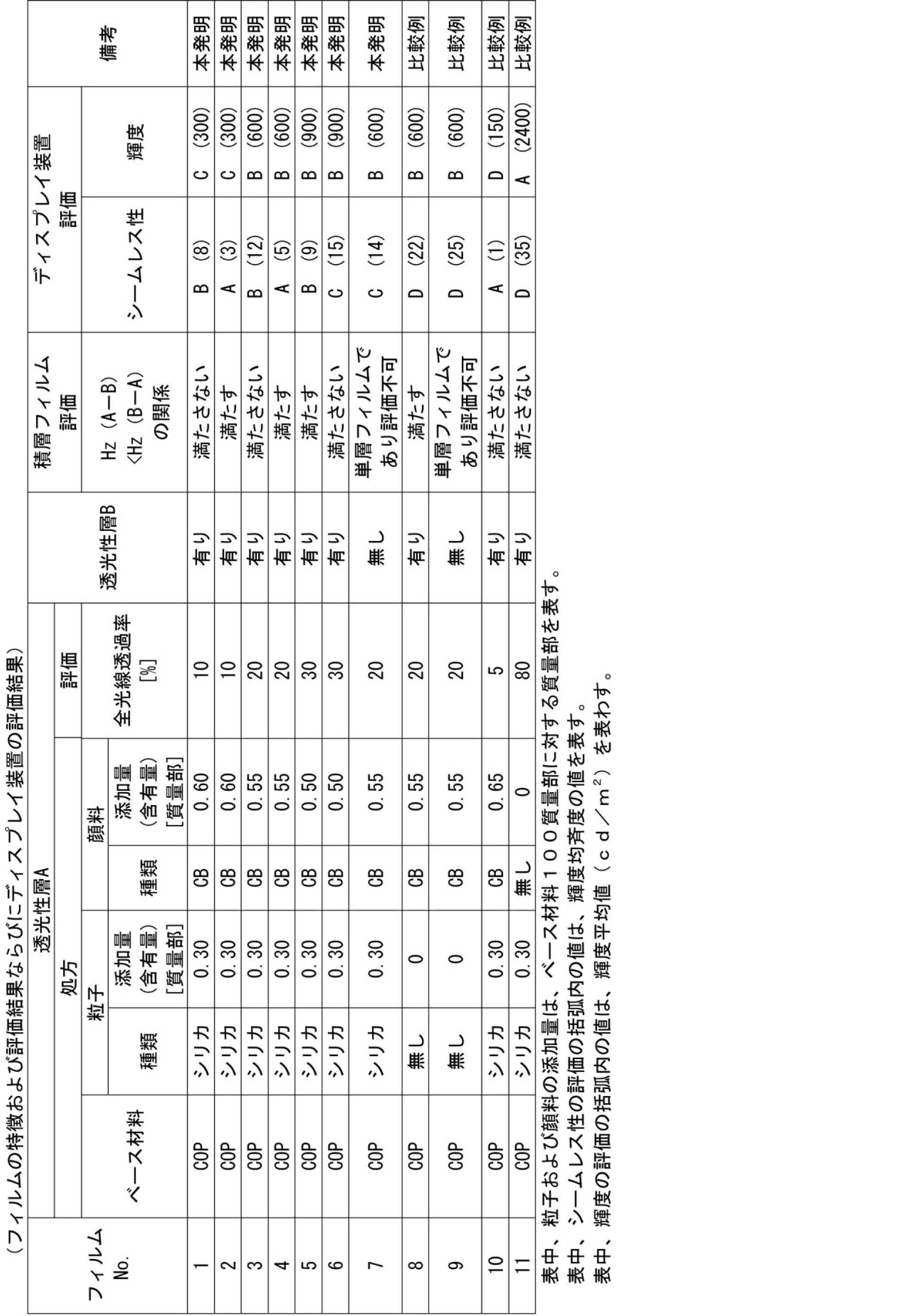
2 積層フィルム
3 透光性層B
3’ 透光性層Bの母体(基礎)となる層またはフィルム
4 ハードコート層
10 パネルユニット
11 LEDモジュール
12 接着層
20 独立モジュール型のディスプレイ装置
100 積層体(積層フィルム)
110 支持体(例えば、透光性層B等の基材層)
200 製造装置
201 支持体(例えば、透光性層B等の基材層)のロール体
210 供給部
220 塗布部
221 バックアップロール
222 塗布ヘッド
223 減圧室
230 乾燥部
231 乾燥室
232 乾燥用気体の導入口
233 排出口
240 冷却部
241 冷却室
242 冷却風入口
243 冷却風出口
250 巻き取り部
251 積層体(積層フィルム)のロール体
a、b、c、d 搬送ロール。
Claims (13)
- 粒子および着色剤を含み、全光線透過率が10%以上30%以下である、透光性層を含む、
複数のパネルユニットで構成される表示面を有するディスプレイ装置に用いられる、光学フィルム。 - 前記透光性層は、樹脂フィルムである、請求項1に記載の光学フィルム。
- 前記透光性層の全光線透過率が15%以上25%以下である、請求項1または2に記載の光学フィルム。
- 前記粒子は、無機酸化物粒子である、請求項1~3のいずれか1項に記載の光学フィルム。
- 前記着色剤は、顔料である、請求項1~4のいずれか1項に記載の光学フィルム。
- 前記透光性層は、透光性層Aであり、
基材層をさらに含む、
請求項1~5のいずれか1項に記載の光学フィルム。 - 前記基材層は、樹脂フィルムである、請求項6に記載の光学フィルム。
- 前記基材層は、透光性層Bであり、
前記透光性層A上に、前記透光性層Bが配置されており、
前記透光性層Aと、前記透光性層Bとは、1つの透光性層Aと、1つの透光性層Bとの積層体のヘイズを測定した際に、前記透光性層A側から光を入射させたときの値Hz(A-B)(%)と、前記透光性層B側から光を入射させたときの値Hz(B-A)(%)とが、Hz(A-B)<Hz(B-A)となる関係を満たす、
請求項6または7に記載の光学フィルム。 - 発光モジュールと、前記発光モジュールよりも表示面側に配置される、請求項1~5のいずれか1項に記載の光学フィルムと、を有する、
複数のパネルユニットで構成される表示面を有するディスプレイ装置に用いられる、パネルユニット。 - 発光モジュールと、前記発光モジュールよりも表示面側に配置される、請求項6~8のいずれか1項に記載の光学フィルムと、を有し、
前記透光性層Aよりも前記表示面側に前記基材層が配置されている、
複数のパネルユニットで構成される表示面を有するディスプレイ装置に用いられる、パネルユニット。 - 前記発光モジュールは、LED素子を含む、請求項9または10に記載のパネルユニット。
- 前記LED素子は、LED発光チップと、前記LED発光チップを被覆する樹脂カバーとを有し、
前記LED素子の幅(W)および奥行き(D)は、いずれも300μm以下であり、前記LED素子の高さ(H)は、200μm以下であり、
個々の前記LED素子の配置間隔は、0.03mm以上100mm以下である、請求項11に記載のパネルユニット。 - 請求項9~12のいずれか1項に記載のパネルユニットの複数個で構成される表示面を有する、ディスプレイ装置。
Priority Applications (3)
| Application Number | Priority Date | Filing Date | Title |
|---|---|---|---|
| CN202180048375.3A CN115812168B (en) | 2020-07-07 | 2021-06-07 | Optical film, panel unit, and display device |
| KR1020237000475A KR102866202B1 (ko) | 2020-07-07 | 2021-06-07 | 광학 필름, 패널 유닛, 및 디스플레이 장치 |
| JP2022534959A JP7276613B2 (ja) | 2020-07-07 | 2021-06-07 | 光学フィルム、パネルユニット、およびディスプレイ装置 |
Applications Claiming Priority (2)
| Application Number | Priority Date | Filing Date | Title |
|---|---|---|---|
| JP2020117339 | 2020-07-07 | ||
| JP2020-117339 | 2020-07-07 |
Publications (1)
| Publication Number | Publication Date |
|---|---|
| WO2022009581A1 true WO2022009581A1 (ja) | 2022-01-13 |
Family
ID=79552406
Family Applications (1)
| Application Number | Title | Priority Date | Filing Date |
|---|---|---|---|
| PCT/JP2021/021596 Ceased WO2022009581A1 (ja) | 2020-07-07 | 2021-06-07 | 光学フィルム、パネルユニット、およびディスプレイ装置 |
Country Status (4)
| Country | Link |
|---|---|
| JP (2) | JP7276613B2 (ja) |
| KR (1) | KR102866202B1 (ja) |
| TW (1) | TWI780774B (ja) |
| WO (1) | WO2022009581A1 (ja) |
Citations (4)
| Publication number | Priority date | Publication date | Assignee | Title |
|---|---|---|---|---|
| WO2015163041A1 (ja) * | 2014-04-21 | 2015-10-29 | コニカミノルタ株式会社 | 面状発光ユニット |
| JP2019028370A (ja) * | 2017-08-02 | 2019-02-21 | 大日本印刷株式会社 | 表示装置用前面板及び表示装置 |
| JP2019066613A (ja) * | 2017-09-29 | 2019-04-25 | 大日本印刷株式会社 | 表示パネルおよびタイリング表示装置 |
| JP2019204905A (ja) * | 2018-05-24 | 2019-11-28 | 大日本印刷株式会社 | 自発光型表示体 |
Family Cites Families (3)
| Publication number | Priority date | Publication date | Assignee | Title |
|---|---|---|---|---|
| KR20150097359A (ko) * | 2014-02-18 | 2015-08-26 | 주식회사 엘지화학 | 봉지 필름 및 이를 포함하는 유기전자장치 |
| JP7338307B2 (ja) | 2018-08-07 | 2023-09-05 | 三菱ケミカル株式会社 | フィルム積層体 |
| KR102676868B1 (ko) * | 2018-11-16 | 2024-06-21 | 삼성전자주식회사 | 디스플레이 모듈, 디스플레이 장치 및 디스플레이 장치의 제조 방법 |
-
2021
- 2021-06-07 JP JP2022534959A patent/JP7276613B2/ja active Active
- 2021-06-07 WO PCT/JP2021/021596 patent/WO2022009581A1/ja not_active Ceased
- 2021-06-07 KR KR1020237000475A patent/KR102866202B1/ko active Active
- 2021-06-16 TW TW110121853A patent/TWI780774B/zh active
-
2023
- 2023-05-02 JP JP2023076132A patent/JP7533682B2/ja active Active
Patent Citations (4)
| Publication number | Priority date | Publication date | Assignee | Title |
|---|---|---|---|---|
| WO2015163041A1 (ja) * | 2014-04-21 | 2015-10-29 | コニカミノルタ株式会社 | 面状発光ユニット |
| JP2019028370A (ja) * | 2017-08-02 | 2019-02-21 | 大日本印刷株式会社 | 表示装置用前面板及び表示装置 |
| JP2019066613A (ja) * | 2017-09-29 | 2019-04-25 | 大日本印刷株式会社 | 表示パネルおよびタイリング表示装置 |
| JP2019204905A (ja) * | 2018-05-24 | 2019-11-28 | 大日本印刷株式会社 | 自発光型表示体 |
Also Published As
| Publication number | Publication date |
|---|---|
| TW202212936A (zh) | 2022-04-01 |
| KR20230019204A (ko) | 2023-02-07 |
| KR102866202B1 (ko) | 2025-09-29 |
| JP2023106441A (ja) | 2023-08-01 |
| JPWO2022009581A1 (ja) | 2022-01-13 |
| CN115812168A (zh) | 2023-03-17 |
| JP7533682B2 (ja) | 2024-08-14 |
| JP7276613B2 (ja) | 2023-05-18 |
| TWI780774B (zh) | 2022-10-11 |
Similar Documents
| Publication | Publication Date | Title |
|---|---|---|
| CN100383562C (zh) | 低反射率亮度增强多层光学膜及有机发光二极管显示器 | |
| TWI730138B (zh) | 光學積層體及顯示裝置 | |
| EP3128350B1 (en) | Wavelength conversion sheet, backlight unit, and film for protecting luminescent substance | |
| CN109477617B (zh) | 背光用薄膜 | |
| WO2001057833A1 (en) | Filter for displaying, display unit and production method therefor | |
| CN105531535A (zh) | 波长转换片和背光单元 | |
| WO2015084018A1 (ko) | 광학 부재 및 이를 구비하는 표시 장치 | |
| CN105493624B (zh) | El用光提取薄膜、el用光提取薄膜的制造方法以及面发光体 | |
| CN107003562A (zh) | 液晶显示装置和偏光板 | |
| CN113136149B (zh) | 用于显示装置的亮度均匀性的保护膜及包括其的显示装置 | |
| KR102205622B1 (ko) | 광학 적층체 및 면광원 장치 | |
| JP2019079053A (ja) | 偏光子保護フィルム、偏光板及び画像表示装置 | |
| CN115016170B (zh) | 量子点和有机纳米荧光体的复合片及包括其的显示装置 | |
| KR20150109376A (ko) | 광학 부재용 점착제 조성물, 광학 부재용 점착층 및 면광원 장치 | |
| CN114023796A (zh) | 显示面板 | |
| CN110730927A (zh) | 显示装置 | |
| JP2014016589A (ja) | 偏光板一体型導電性光学積層体及びそれを用いた表示装置 | |
| BR112012027183A2 (pt) | película de composto óptico para módulo de luz de fundo. | |
| KR20190075756A (ko) | 편광판 및 이를 포함하는 광학표시장치 | |
| JP6862814B2 (ja) | 量子ドットシートを有するバックライト、及び該バックライトを備えた液晶表示装置 | |
| CN115016171B (zh) | 量子点和有机纳米荧光体的复合片及包括其的显示装置 | |
| KR20190097914A (ko) | 컬러필터 및 이를 포함하는 표시 장치 | |
| KR102866202B1 (ko) | 광학 필름, 패널 유닛, 및 디스플레이 장치 | |
| KR20180007870A (ko) | 편광판 일체형 색변환 필름 및 이를 포함하는 디스플레이 장치 | |
| CN115812168B (en) | Optical film, panel unit, and display device |
Legal Events
| Date | Code | Title | Description |
|---|---|---|---|
| 121 | Ep: the epo has been informed by wipo that ep was designated in this application |
Ref document number: 21838617 Country of ref document: EP Kind code of ref document: A1 |
|
| ENP | Entry into the national phase |
Ref document number: 2022534959 Country of ref document: JP Kind code of ref document: A |
|
| ENP | Entry into the national phase |
Ref document number: 20237000475 Country of ref document: KR Kind code of ref document: A |
|
| NENP | Non-entry into the national phase |
Ref country code: DE |
|
| 122 | Ep: pct application non-entry in european phase |
Ref document number: 21838617 Country of ref document: EP Kind code of ref document: A1 |