WO2022004504A1 - 積層基板 - Google Patents
積層基板 Download PDFInfo
- Publication number
- WO2022004504A1 WO2022004504A1 PCT/JP2021/023697 JP2021023697W WO2022004504A1 WO 2022004504 A1 WO2022004504 A1 WO 2022004504A1 JP 2021023697 W JP2021023697 W JP 2021023697W WO 2022004504 A1 WO2022004504 A1 WO 2022004504A1
- Authority
- WO
- WIPO (PCT)
- Prior art keywords
- thermoplastic resin
- conductor
- resin layer
- layer
- interlayer
- Prior art date
- Legal status (The legal status is an assumption and is not a legal conclusion. Google has not performed a legal analysis and makes no representation as to the accuracy of the status listed.)
- Ceased
Links
Images





Classifications
-
- H—ELECTRICITY
- H05—ELECTRIC TECHNIQUES NOT OTHERWISE PROVIDED FOR
- H05K—PRINTED CIRCUITS; CASINGS OR CONSTRUCTIONAL DETAILS OF ELECTRIC APPARATUS; MANUFACTURE OF ASSEMBLAGES OF ELECTRICAL COMPONENTS
- H05K3/00—Apparatus or processes for manufacturing printed circuits
- H05K3/46—Manufacturing multilayer circuits
- H05K3/4611—Manufacturing multilayer circuits by laminating two or more circuit boards
- H05K3/4626—Manufacturing multilayer circuits by laminating two or more circuit boards characterised by the insulating layers or materials
- H05K3/4632—Manufacturing multilayer circuits by laminating two or more circuit boards characterised by the insulating layers or materials laminating thermoplastic or uncured resin sheets comprising printed circuits without added adhesive materials between the sheets
-
- H—ELECTRICITY
- H05—ELECTRIC TECHNIQUES NOT OTHERWISE PROVIDED FOR
- H05K—PRINTED CIRCUITS; CASINGS OR CONSTRUCTIONAL DETAILS OF ELECTRIC APPARATUS; MANUFACTURE OF ASSEMBLAGES OF ELECTRICAL COMPONENTS
- H05K1/00—Printed circuits
- H05K1/02—Details
- H05K1/0296—Conductive pattern lay-out details not covered by sub groups H05K1/02 - H05K1/0295
- H05K1/0298—Multilayer circuits
-
- H—ELECTRICITY
- H05—ELECTRIC TECHNIQUES NOT OTHERWISE PROVIDED FOR
- H05K—PRINTED CIRCUITS; CASINGS OR CONSTRUCTIONAL DETAILS OF ELECTRIC APPARATUS; MANUFACTURE OF ASSEMBLAGES OF ELECTRICAL COMPONENTS
- H05K3/00—Apparatus or processes for manufacturing printed circuits
- H05K3/40—Forming printed elements for providing electric connections to or between printed circuits
- H05K3/4038—Through-connections; Vertical interconnect access [VIA] connections
- H05K3/4053—Through-connections; Vertical interconnect access [VIA] connections by thick-film techniques
- H05K3/4069—Through-connections; Vertical interconnect access [VIA] connections by thick-film techniques for via connections in organic insulating substrates
-
- H—ELECTRICITY
- H05—ELECTRIC TECHNIQUES NOT OTHERWISE PROVIDED FOR
- H05K—PRINTED CIRCUITS; CASINGS OR CONSTRUCTIONAL DETAILS OF ELECTRIC APPARATUS; MANUFACTURE OF ASSEMBLAGES OF ELECTRICAL COMPONENTS
- H05K1/00—Printed circuits
- H05K1/02—Details
- H05K1/0213—Electrical arrangements not otherwise provided for
- H05K1/0216—Reduction of cross-talk, noise or electromagnetic interference
- H05K1/0218—Reduction of cross-talk, noise or electromagnetic interference by printed shielding conductors, ground planes or power plane
- H05K1/0219—Printed shielding conductors for shielding around or between signal conductors, e.g. coplanar or coaxial printed shielding conductors
-
- H—ELECTRICITY
- H05—ELECTRIC TECHNIQUES NOT OTHERWISE PROVIDED FOR
- H05K—PRINTED CIRCUITS; CASINGS OR CONSTRUCTIONAL DETAILS OF ELECTRIC APPARATUS; MANUFACTURE OF ASSEMBLAGES OF ELECTRICAL COMPONENTS
- H05K2201/00—Indexing scheme relating to printed circuits covered by H05K1/00
- H05K2201/01—Dielectrics
- H05K2201/0104—Properties and characteristics in general
- H05K2201/0129—Thermoplastic polymer, e.g. auto-adhesive layer; Shaping of thermoplastic polymer
-
- H—ELECTRICITY
- H05—ELECTRIC TECHNIQUES NOT OTHERWISE PROVIDED FOR
- H05K—PRINTED CIRCUITS; CASINGS OR CONSTRUCTIONAL DETAILS OF ELECTRIC APPARATUS; MANUFACTURE OF ASSEMBLAGES OF ELECTRICAL COMPONENTS
- H05K2201/00—Indexing scheme relating to printed circuits covered by H05K1/00
- H05K2201/01—Dielectrics
- H05K2201/0137—Materials
- H05K2201/0141—Liquid crystal polymer [LCP]
-
- H—ELECTRICITY
- H05—ELECTRIC TECHNIQUES NOT OTHERWISE PROVIDED FOR
- H05K—PRINTED CIRCUITS; CASINGS OR CONSTRUCTIONAL DETAILS OF ELECTRIC APPARATUS; MANUFACTURE OF ASSEMBLAGES OF ELECTRICAL COMPONENTS
- H05K2201/00—Indexing scheme relating to printed circuits covered by H05K1/00
- H05K2201/07—Electric details
- H05K2201/0707—Shielding
- H05K2201/0715—Shielding provided by an outer layer of PCB
-
- H—ELECTRICITY
- H05—ELECTRIC TECHNIQUES NOT OTHERWISE PROVIDED FOR
- H05K—PRINTED CIRCUITS; CASINGS OR CONSTRUCTIONAL DETAILS OF ELECTRIC APPARATUS; MANUFACTURE OF ASSEMBLAGES OF ELECTRICAL COMPONENTS
- H05K2201/00—Indexing scheme relating to printed circuits covered by H05K1/00
- H05K2201/09—Shape and layout
- H05K2201/09209—Shape and layout details of conductors
- H05K2201/0929—Conductive planes
- H05K2201/09363—Conductive planes wherein only contours around conductors are removed for insulation
-
- H—ELECTRICITY
- H05—ELECTRIC TECHNIQUES NOT OTHERWISE PROVIDED FOR
- H05K—PRINTED CIRCUITS; CASINGS OR CONSTRUCTIONAL DETAILS OF ELECTRIC APPARATUS; MANUFACTURE OF ASSEMBLAGES OF ELECTRICAL COMPONENTS
- H05K2201/00—Indexing scheme relating to printed circuits covered by H05K1/00
- H05K2201/09—Shape and layout
- H05K2201/09209—Shape and layout details of conductors
- H05K2201/095—Conductive through-holes or vias
- H05K2201/09509—Blind vias, i.e. vias having one side closed
Definitions
- the present invention relates to a laminated substrate.
- a plurality of signal transmission lines and a power transmission line are combined as a laminated insulator in which a plurality of insulator layers are laminated.
- a line, the plurality of signal transmission lines including at least a first signal transmission line and a second signal transmission line, a first signal transmission line including a first signal conductor pattern, and a second signal transmission line a second.
- the power transmission line includes a signal conductor pattern, and the power transmission line is composed of a power transmission conductor pattern formed along a plurality of layers of a laminated insulator and an interlayer connecting conductor connecting these power transmission conductor patterns.
- the pattern, the second signal conductor pattern and the power transmission conductor pattern are formed in different layers of the laminated insulator and in parallel, and the first signal conductor pattern and the second signal conductor pattern insulate the first ground conductor.
- a composite transmission line is disclosed, which is arranged so as to be sandwiched in the stacking direction of the body layers and is arranged on the side of the first signal conductor pattern.
- the signal conductor pattern, the power transmission conductor pattern, and the ground conductor are each connected to the interlayer connecting conductor.
- the connectivity between each of the above and the interlayer connection conductor may be reduced.
- Such a decrease in connectivity with the interlayer connecting conductor has a greater influence on characteristics such as high frequency characteristics with respect to the signal conductor pattern or the power transmission conductor pattern than with the ground conductor.
- the present invention has been made to solve the above problems, and an object of the present invention is to provide a laminated substrate having excellent connectivity between a conductor pattern for signals or power transmission and an interlayer connection conductor. be.
- the laminated substrate of the present invention has a first laminated portion made of at least one first thermoplastic resin layer and a second laminated portion made of at least one second thermoplastic resin layer adjacent to the first laminated portion.
- a resin laminate having a laminated structure including the above in the lamination direction and having a first main surface on the first laminated portion side and a second main surface on the second laminated portion side facing the laminated direction.
- a surface electrode provided on the first main surface of the resin laminate, and a first conductor pattern for signals or power transmission provided between the first laminated portion and the second laminated portion.
- Provided with at least one first interlayer connection conductor provided so as to penetrate the first thermoplastic resin layer in the stacking direction and electrically connecting the surface electrode and the first conductor pattern.
- the first interlayer connecting conductor contains a resin and at least one metal element, is equal to or higher than the minimum melting point of the melting points of the metal elements contained in the first interlayer connecting conductor, and is the first thermoplastic resin layer.
- the storage elasticity of the first thermoplastic resin layer is lower than the storage elasticity of the second thermoplastic resin layer at a measurement temperature equal to or lower than the melting point of the second thermoplastic resin layer.
- FIG. 1 It is sectional drawing which shows an example of the conductive paste filling process in the via hole of the 1st thermoplastic resin sheet about the manufacturing method of the laminated substrate of Embodiment 1 of this invention. It is sectional drawing which shows an example of the process of forming a conductor layer on the other surface of the 1st thermoplastic resin sheet about the manufacturing method of the laminated substrate of Embodiment 1 of this invention. It is sectional drawing which shows an example of the conductor layer formation process on one surface of the 2nd thermoplastic resin sheet about the manufacturing method of the laminated substrate of Embodiment 1 of this invention. It is sectional drawing which shows an example of the via hole forming process in the 2nd thermoplastic resin sheet about the manufacturing method of the laminated substrate of Embodiment 1 of this invention. FIG.
- FIG. 5 is a schematic cross-sectional view showing an example of a step of filling a via hole of a second thermoplastic resin sheet with a conductive paste for the method of manufacturing a laminated substrate according to the first embodiment of the present invention.
- It is sectional drawing which shows an example of the process of laminating and thermocompression bonding of the 1st thermoplastic resin sheet and the 2nd thermoplastic resin sheet about the manufacturing method of the laminated substrate of Embodiment 1 of this invention.
- It is sectional drawing which shows an example of the process of laminating and thermocompression bonding of the 1st thermoplastic resin sheet and the 2nd thermoplastic resin sheet about the manufacturing method of the laminated substrate of Embodiment 1 of this invention.
- It is sectional drawing which shows the laminated substrate of the modification of Embodiment 1 of this invention.
- the laminated substrate of the present invention will be described.
- the present invention is not limited to the following configuration, and may be appropriately modified without departing from the gist of the present invention.
- a combination of a plurality of individual preferred configurations described below is also the present invention.
- FIG. 1 is an exploded perspective schematic view showing a laminated substrate according to the first embodiment of the present invention.
- FIG. 2 is a schematic cross-sectional view showing a portion corresponding to the line segments A1-A2 in FIG.
- FIG. 3 is a schematic cross-sectional view showing a portion corresponding to the line segments B1-B2 in FIG.
- the laminated substrate 1 includes a resin laminate 10, a surface electrode 20a, a surface electrode 20b, and a first conductor pattern 30 for signal or power transmission. It has a first interlayer connection conductor 41a and a first interlayer connection conductor 41b.
- the resin laminated body 10 has a laminated structure including the first laminated portion 11 and the second laminated portion 12 adjacent to the first laminated portion 11 in the laminated direction (vertical direction in FIGS. 1, 2, and 3). Have.
- the first laminated portion 11 is made of a first thermoplastic resin layer 11a.
- the second laminated portion 12 is made of a second thermoplastic resin layer 12a.
- thermoplastic resin constituting the first thermoplastic resin layer 11a and the second thermoplastic resin layer 12a examples include liquid crystal polymer (LCP), fluororesin, thermoplastic polyimide resin, polyetheretherketone resin (PEEK), and polyphenylene. Examples thereof include sulfide resin (PPS).
- thermoplastic resins constituting the first thermoplastic resin layer 11a and the second thermoplastic resin layer 12a may be the same as each other or may be different from each other.
- the first thermoplastic resin layer 11a and the second thermoplastic resin layer 12a may each contain a liquid crystal polymer as a main component. Since the liquid crystal polymer has lower water absorption than other thermoplastic resins, when the first thermoplastic resin layer 11a and the second thermoplastic resin layer 12a each contain the liquid crystal polymer as a main component in the laminated substrate 1, the water content is reduced. Changes in electrical characteristics due to intrusion are less likely to occur.
- the molecular weight of the liquid crystal polymer constituting the first thermoplastic resin layer 11a and the second thermoplastic resin layer are obtained. It is preferable that the molecular weights of the liquid crystal polymers constituting 12a are different from each other.
- the storage elastic modulus of the first thermoplastic resin layer 11a can be changed to the second thermoplastic resin layer. It can be lower than the storage elastic modulus of 12a.
- the first laminated portion is composed of at least one first thermoplastic resin layer. That is, the first laminated portion is composed of only the first thermoplastic resin layer, and includes at least one first thermoplastic resin layer.
- the second laminated portion is composed of at least one second thermoplastic resin layer. That is, the second laminated portion is composed of only the second thermoplastic resin layer, and includes at least one second thermoplastic resin layer.
- the first thermoplastic resin layer constituting the first laminated portion and the second thermoplastic resin layer constituting the second laminated portion may be composed of the same thermoplastic resin.
- the first thermoplastic resin layer and the second thermoplastic resin layer may each contain a liquid crystal polymer as a main component.
- the molecular weight of the liquid crystal polymer constituting the first thermoplastic resin layer and the molecular weight of the liquid crystal polymer constituting the second thermoplastic resin layer are different from each other.
- the resin laminated body 10 has a first main surface 10a on the first laminated portion 11 side and a second main surface 10b on the second laminated portion 12 side facing in the laminating direction. More specifically, the first main surface 10a of the resin laminate 10 corresponds to the surface of the first thermoplastic resin layer 11a opposite to the second thermoplastic resin layer 12a. Further, the second main surface 10b of the resin laminate 10 corresponds to the surface of the second thermoplastic resin layer 12a on the opposite side of the first thermoplastic resin layer 11a.
- the surface electrode 20a is provided on the first main surface 10a of the resin laminate 10.
- the surface electrode 20b is provided on the first main surface 10a of the resin laminate 10 at a position separated from the surface electrode 20a.
- Examples of the constituent materials of the surface electrode 20a and the surface electrode 20b include copper, silver, aluminum, stainless steel, nickel, gold, and alloys containing at least one of these metals.
- the surface electrode 20a and the surface electrode 20b each contain copper.
- the surface electrode 20a and the surface electrode 20b are each preferably made of a conductor foil, and it is particularly preferable that the surface electrode 20a is made of a copper foil among the conductor foils.
- the constituent materials of the surface electrode 20a and the surface electrode 20b are preferably the same as each other, but may be different from each other.
- the first conductor pattern 30 is provided between the first laminated portion 11 and the second laminated portion 12.
- the first conductor pattern 30 is preferably provided so as to straddle the boundary between the first thermoplastic resin layer 11a and the second thermoplastic resin layer 12a.
- the interface between the first conductor pattern 30 and the first thermoplastic resin layer 11a and the interface between the first conductor pattern 30 and the second thermoplastic resin layer 12a become the first thermoplastic resin layer 11a and the second. Since it deviates from the interface with the thermoplastic resin layer 12a in the stacking direction, peeling at the interface between the first conductor pattern 30 and the first thermoplastic resin layer 11a, and the peeling between the first conductor pattern 30 and the second thermoplastic resin layer 12a Peeling at the interface with and is suppressed.
- the boundary between the first thermoplastic resin layer 11a and the second thermoplastic resin layer 12a can be observed by infrared spectroscopy or interconnected with respect to the cross section along the stacking direction as shown in FIGS. 2 and 3. It can be judged by observing the position of the end of the conductor.
- one surface of the surface electrode 20a and the surface electrode 20b side is connected to the first interlayer connection conductor 41a and the first interlayer connection conductor 41b in the stacking direction.
- the surface electrode 20a and the other surface on the opposite side to the surface electrode 20b are not connected to the interlayer connecting conductor.
- Examples of the constituent material of the first conductor pattern 30 include copper, silver, aluminum, stainless steel, nickel, gold, and alloys containing at least one of these metals.
- the first conductor pattern 30 preferably contains copper.
- the first conductor pattern 30 is preferably made of a conductor foil, and is particularly preferably made of a copper foil among the conductor foils.
- the first interlayer connection conductor 41a is provided so as to penetrate the first thermoplastic resin layer 11a in the stacking direction. As a result, the first interlayer connection conductor 41a electrically connects the surface electrode 20a and the first conductor pattern 30.
- the first interlayer connection conductor 41b is provided so as to penetrate the first thermoplastic resin layer 11a at a position separated from the first interlayer connection conductor 41a in the stacking direction. As a result, the first interlayer connection conductor 41b electrically connects the surface electrode 20b and the first conductor pattern 30.
- the lengths of the first interlayer connection conductor 41a and the first interlayer connection conductor 41b in the transmission direction orthogonal to the stacking direction, more specifically, in the direction in which the first interlayer connection conductor 41a and the first interlayer connection conductor 41b face each other. are each smaller than the length of the first conductor pattern 30.
- the first interlayer connecting conductor 41a and the first interlayer connecting conductor 41b each contain a resin and at least one metal element.
- the first interlayer connection conductor 41a and the first interlayer connection conductor 41b are, for example, filled with a conductive paste in a via hole provided so as to penetrate the first thermoplastic resin layer 11a, and then heat-treated. It is formed as a sintered body of a conductive paste.
- the resin contained in the first interlayer connection conductor 41a and the first interlayer connection conductor 41b is at least one selected from the group consisting of an epoxy resin, a phenol resin, a polyimide resin, a silicon resin or a modified resin thereof, and an acrylic resin. It is preferable to contain at least one thermoplastic resin selected from the group consisting of a thermosetting resin, a polyamide resin, a polystyrene resin, a polymethacrylic resin, a polycarbonate resin, and a cellulose-based resin.
- Examples of the metal element contained in the first interlayer connecting conductor 41a and the first interlayer connecting conductor 41b include copper, tin, silver and the like.
- the first interlayer connecting conductor 41a and the first interlayer connecting conductor 41b each preferably contain copper as a metal element, and more preferably contain copper and tin as metal elements.
- the first interlayer connecting conductor 41a preferably contains tin as a metal element having the minimum melting point among the melting points of the metal elements contained in the first interlayer connecting conductor 41a.
- the first interlayer connecting conductor 41b preferably contains tin as a metal element having the minimum melting point among the melting points of the metal elements contained in the first interlayer connecting conductor 41b.
- the resins contained in the first interlayer connection conductor 41a and the first interlayer connection conductor 41b are preferably the same as each other, but may be different from each other. Further, the metal elements contained in the first interlayer connecting conductor 41a and the first interlayer connecting conductor 41b are preferably the same as each other, but may be different from each other. That is, it is preferable that the first interlayer connecting conductor 41a and the first interlayer connecting conductor 41b contain the same resin and the same metal element.
- the laminated substrate 1 may further have a second conductor pattern 50 for ground.
- the second conductor pattern 50 is provided on the second main surface 10b side of the resin laminate 10 with respect to the first conductor pattern 30. More specifically, the second conductor pattern 50 is provided on the second main surface 10b of the resin laminate 10. The second conductor pattern 50 may be provided inside the resin laminate 10 instead of on the second main surface 10b of the resin laminate 10.
- the second conductor pattern 50 overlaps with the first conductor pattern 30 when viewed from the stacking direction.
- Examples of the constituent material of the second conductor pattern 50 include copper, silver, aluminum, stainless steel, nickel, gold, and alloys containing at least one of these metals.
- the second conductor pattern 50 preferably contains copper.
- the second conductor pattern 50 is preferably made of a conductor foil, and is particularly preferably made of a copper foil among the conductor foils.
- the laminated substrate 1 further includes a second interlayer connecting conductor 42a, a second interlayer connecting conductor 42b, a second interlayer connecting conductor 42c, and a second interlayer connecting conductor 42d. You may be doing it.
- the second interlayer connection conductor 42a and the second interlayer connection conductor 42b are provided so as to penetrate the second thermoplastic resin layer 12a at a position sandwiching the first interlayer connection conductor 41a when viewed from the stacking direction. ing. As a result, the second interlayer connecting conductor 42a and the second interlayer connecting conductor 42b are connected to the second conductor pattern 50.
- the second interlayer connection conductor 42c and the second interlayer connection conductor 42d are provided so as to penetrate the second thermoplastic resin layer 12a at a position sandwiching the first interlayer connection conductor 41b when viewed from the stacking direction. ing. As a result, the second interlayer connecting conductor 42c and the second interlayer connecting conductor 42d are connected to the second conductor pattern 50.
- the second interlayer connecting conductor 42a, the second interlayer connecting conductor 42b, the second interlayer connecting conductor 42c, and the second interlayer connecting conductor 42d each contain a resin and at least one metal element.
- the second interlayer connecting conductor 42a, the second interlayer connecting conductor 42b, the second interlayer connecting conductor 42c, and the second interlayer connecting conductor 42d each penetrate, for example, the second thermoplastic resin layer 12a.
- the provided via holes are filled with the conductive paste and then heat-treated to form a sintered body of the conductive paste.
- the resin contained in the second interlayer connection conductor 42a, the second interlayer connection conductor 42b, the second interlayer connection conductor 42c, and the second interlayer connection conductor 42d is an epoxy resin, a phenol resin, a polyimide resin, a silicon resin or a modified resin thereof.
- Examples of the metal element contained in the second interlayer connecting conductor 42a, the second interlayer connecting conductor 42b, the second interlayer connecting conductor 42c, and the second interlayer connecting conductor 42d include copper, tin, silver and the like.
- the second interlayer connecting conductor 42a, the second interlayer connecting conductor 42b, the second interlayer connecting conductor 42c, and the second interlayer connecting conductor 42d each preferably contain copper as a metal element, and copper and tin as metal elements. It is more preferable to include it.
- the resins contained in the second interlayer connecting conductor 42a, the second interlayer connecting conductor 42b, the second interlayer connecting conductor 42c, and the second interlayer connecting conductor 42d are preferably the same as each other, but may be different from each other. .. Further, the metal elements contained in the second interlayer connecting conductor 42a, the second interlayer connecting conductor 42b, the second interlayer connecting conductor 42c, and the second interlayer connecting conductor 42d are preferably the same as each other, but are different from each other. You may. That is, it is preferable that the second interlayer connecting conductor 42a, the second interlayer connecting conductor 42b, the second interlayer connecting conductor 42c, and the second interlayer connecting conductor 42d contain the same resin and the same metal element as each other.
- the laminated substrate 1 may further have a ground electrode 60.
- the ground electrode 60 is provided on the first main surface 10a of the resin laminate 10 at a position separated from the surface electrode 20a and the surface electrode 20b.
- Examples of the constituent material of the ground electrode 60 include copper, silver, aluminum, stainless steel, nickel, gold, and alloys containing at least one of these metals.
- the ground electrode 60 preferably contains copper.
- the ground electrode 60 is preferably made of a conductor foil, and is particularly preferably made of a copper foil among the conductor foils.
- the laminated substrate 1 further includes a third interlayer connecting conductor 43a, a third interlayer connecting conductor 43b, a third interlayer connecting conductor 43c, and a third interlayer connecting conductor 43d. You may be doing it.
- the third interlayer connection conductor 43a and the third interlayer connection conductor 43b are provided so as to penetrate the first thermoplastic resin layer 11a at a position sandwiching the first interlayer connection conductor 41a when viewed from the stacking direction. ing. As a result, the third interlayer connecting conductor 43a and the third interlayer connecting conductor 43b are connected to the ground electrode 60.
- the third interlayer connection conductor 43c and the third interlayer connection conductor 43d are provided so as to penetrate the first thermoplastic resin layer 11a at positions sandwiching the first interlayer connection conductor 41b when viewed from the stacking direction. ing. As a result, the third interlayer connecting conductor 43c and the third interlayer connecting conductor 43d are connected to the ground electrode 60.
- the third interlayer connecting conductor 43a, the third interlayer connecting conductor 43b, the third interlayer connecting conductor 43c, and the third interlayer connecting conductor 43d each contain a resin and at least one metal element.
- the third interlayer connecting conductor 43a, the third interlayer connecting conductor 43b, the third interlayer connecting conductor 43c, and the third interlayer connecting conductor 43d each penetrate, for example, the first thermoplastic resin layer 11a.
- the provided via holes are filled with the conductive paste and then heat-treated to form a sintered body of the conductive paste.
- the resin contained in the third interlayer connection conductor 43a, the third interlayer connection conductor 43b, the third interlayer connection conductor 43c, and the third interlayer connection conductor 43d is an epoxy resin, a phenol resin, a polyimide resin, a silicon resin or a modified resin thereof.
- Examples of the metal element contained in the third interlayer connecting conductor 43a, the third interlayer connecting conductor 43b, the third interlayer connecting conductor 43c, and the third interlayer connecting conductor 43d include copper, tin, silver and the like.
- the third interlayer connecting conductor 43a, the third interlayer connecting conductor 43b, the third interlayer connecting conductor 43c, and the third interlayer connecting conductor 43d each preferably contain copper as a metal element, and copper and tin are used as metal elements. It is more preferable to include it.
- the resins contained in the third interlayer connecting conductor 43a, the third interlayer connecting conductor 43b, the third interlayer connecting conductor 43c, and the third interlayer connecting conductor 43d are preferably the same as each other, but may be different from each other. .. Further, the metal elements contained in the third interlayer connecting conductor 43a, the third interlayer connecting conductor 43b, the third interlayer connecting conductor 43c, and the third interlayer connecting conductor 43d are preferably the same as each other, but are different from each other. You may. That is, it is preferable that the third interlayer connecting conductor 43a, the third interlayer connecting conductor 43b, the third interlayer connecting conductor 43c, and the third interlayer connecting conductor 43d contain the same resin and the same metal element.
- the laminated substrate 1 may further have a connecting conductor layer 70a, a connecting conductor layer 70b, a connecting conductor layer 70c, and a connecting conductor layer 70d.
- the connecting conductor layer 70a, the connecting conductor layer 70b, the connecting conductor layer 70c, and the connecting conductor layer 70d are provided at positions separated from each other between the first laminated portion 11 and the second laminated portion 12, respectively. ..
- the connecting conductor layer 70a, the connecting conductor layer 70b, the connecting conductor layer 70c, and the connecting conductor layer 70d are separated from each other across the boundary between the first thermoplastic resin layer 11a and the second thermoplastic resin layer 12a, respectively. It is preferably provided at a position. As a result, the interface between each connecting conductor layer and the first thermoplastic resin layer 11a and the interface between each connecting conductor layer and the second thermoplastic resin layer 12a become the first thermoplastic resin layer 11a and the second thermoplastic.
- the connecting conductor layer 70a electrically connects the second interlayer connecting conductor 42a and the third interlayer connecting conductor 43a.
- the connecting conductor layer 70b electrically connects the second interlayer connecting conductor 42b and the third interlayer connecting conductor 43b.
- the connecting conductor layer 70c electrically connects the second interlayer connecting conductor 42c and the third interlayer connecting conductor 43c.
- the connecting conductor layer 70d electrically connects the second interlayer connecting conductor 42d and the third interlayer connecting conductor 43d.
- the lengths of the connecting conductor layer 70a, the connecting conductor layer 70b, the connecting conductor layer 70c, and the connecting conductor layer 70d are each smaller than the length of the first conductor pattern 30.
- the constituent materials of the connecting conductor layer 70a, the connecting conductor layer 70b, the connecting conductor layer 70c, and the connecting conductor layer 70d include, for example, copper, silver, aluminum, stainless steel, nickel, gold, and at least one of these metals. Examples include alloys to be used.
- the connecting conductor layer 70a, the connecting conductor layer 70b, the connecting conductor layer 70c, and the connecting conductor layer 70d each contain copper.
- the connecting conductor layer 70a, the connecting conductor layer 70b, the connecting conductor layer 70c, and the connecting conductor layer 70d are each preferably made of a conductor foil, and it is particularly preferable that the connecting conductor layer is made of a copper foil.
- the constituent materials of the connecting conductor layer 70a, the connecting conductor layer 70b, the connecting conductor layer 70c, and the connecting conductor layer 70d are preferably the same as each other, but may be different from each other.
- the measured temperature is equal to or higher than the minimum melting point of the melting point of the metal element contained in the first interlayer connection conductor and lower than the melting point of the first thermoplastic resin layer and the second thermoplastic resin layer (below).
- the storage elastic modulus of the first thermoplastic resin layer is lower than the storage elastic modulus of the second thermoplastic resin layer.
- the temperature below the melting point of the first thermoplastic resin layer and the second thermoplastic resin layer is the lower melting point of the melting point of the first thermoplastic resin layer and the melting point of the second thermoplastic resin layer. It means the following temperature.
- the melting point of the first thermoplastic resin layer and the melting point of the second thermoplastic resin layer may be the same as each other or may be different from each other.
- the temperature dependence of the storage elastic modulus of the thermoplastic resin layer is measured by dynamic viscoelasticity measurement (DMA).
- DMA dynamic viscoelasticity measurement
- the melting point of the metal element contained in the first interlayer connecting conductor 41a and the first interlayer connecting conductor 41b is equal to or higher than the minimum melting point, and the first thermoplastic resin layer 11a and the second thermoplastic resin layer 12a are formed. At the measured temperature below the melting point, the storage elastic modulus of the first thermoplastic resin layer 11a is lower than the storage elastic modulus of the second thermoplastic resin layer 12a.
- the manufacturing method of the laminated substrate 1 shown in FIG. 1 will be described while illustrating the process of forming the cross section shown in FIG. 2, but other cross sections, for example, the cross section shown in FIG. 3 are shown. The process of formation is similar.
- FIG. 4 is a schematic cross-sectional view showing an example of a step of forming a conductor layer on one surface of a first thermoplastic resin sheet with respect to the method for manufacturing a laminated substrate according to the first embodiment of the present invention.
- the conductor layer 130, the conductor layer 170a, and the conductor layer 170b are formed on one surface of the first thermoplastic resin sheet 111a.
- the first thermoplastic resin sheet 111a serves as the first thermoplastic resin layer 11a.
- the conductor layer 130, the conductor layer 170a, and the conductor layer 170b are the first conductor pattern 30, the connecting conductor layer 70a, and the connecting conductor layer 70b, respectively.
- a conductor layer to be the connecting conductor layer 70c and a conductor layer to be the connecting conductor layer 70d are further formed on one surface of the first thermoplastic resin sheet 111a.
- each conductor layer on one surface of the first thermoplastic resin sheet 111a for example, a method of etching a conductor foil attached to one surface of the first thermoplastic resin sheet 111a, a method of etching each conductor layer. Examples thereof include a method of transferring the conductor foil formed in the pattern to one surface of the first thermoplastic resin sheet 111a.
- the first thermoplastic resin sheet 111a is equal to or higher than the minimum melting point of the melting points of the metal elements contained in the conductive paste 190 described later, and is the first thermoplastic resin sheet 111a and the second thermoplastic resin sheet 112a described later.
- a thermoplastic resin sheet having a storage elasticity lower than that of the second thermoplastic resin sheet 112a is used at a temperature below the melting point.
- the storage elastic modulus of the first thermoplastic resin layer 11a is lower than the storage elastic modulus of the second thermoplastic resin layer 12a at the above-mentioned measured temperature.
- thermoplastic resin constituting the first thermoplastic resin sheet 111a examples include a liquid crystal polymer, a fluororesin, a thermoplastic polyimide resin, a polyether ether ketone resin, and a polyphenylene sulfide resin.
- the first thermoplastic resin sheet 111a may contain a liquid crystal polymer as a main component.
- the storage elastic modulus of the first thermoplastic resin sheet 111a can be adjusted by changing the molecular weight of the liquid crystal polymer, and as will be described later, the storage elastic modulus of the first thermoplastic resin sheet 111a can be adjusted to the second thermoplastic resin. It can be lower than the storage elastic modulus of the sheet 112a.
- the thickness of the first thermoplastic resin sheet 111a is, for example, 10 ⁇ m or more and 2000 ⁇ m or less.
- constituent material of the conductor foil examples include copper, silver, aluminum, stainless steel, nickel, gold, and alloys containing at least one of these metals.
- the conductor foil preferably contains copper. That is, it is preferable that each conductor layer is formed by using a copper foil.
- the thickness of the conductor foil is, for example, 3 ⁇ m or more and 40 ⁇ m or less.
- the thickness of each conductor foil used when forming each conductor layer is preferably the same as each other, but may be different from each other.
- FIG. 5 is a schematic cross-sectional view showing an example of a via hole forming step in a first thermoplastic resin sheet for the method for manufacturing a laminated substrate according to the first embodiment of the present invention.
- via holes 181a, via holes 183a, and via holes 183b are formed so as to penetrate the first thermoplastic resin sheet 111a, respectively. As a result, each part of the conductor layer 130, the conductor layer 170a, and the conductor layer 170b is exposed.
- a via hole that penetrates the first thermoplastic resin sheet 111a and exposes another part of the conductor layer 130 and a part of the conductor layer that becomes the connecting conductor layer 70c are provided.
- a via hole to be exposed and a via hole to expose a part of the conductor layer to be the connecting conductor layer 70d are further formed.
- Examples of the method of forming each via hole in the first thermoplastic resin sheet 111a include a method of irradiating a laser from the other side facing one side of the first thermoplastic resin sheet 111a.
- Such laser irradiation is performed by, for example, a pulse oscillation type carbon dioxide laser irradiation device.
- it is preferable to perform desmear treatment by, for example, oxygen plasma discharge treatment, corona discharge treatment, or the like in order to remove the resin residue.
- the resin residue may be removed by treatment with potassium permanganate or the like.
- each via hole preferably has a tapered shape whose diameter decreases toward each conductor layer formed on one surface of the first thermoplastic resin sheet 111a.
- FIG. 6 is a schematic cross-sectional view showing an example of a step of filling a via hole of a first thermoplastic resin sheet with a conductive paste for the method of manufacturing a laminated substrate according to the first embodiment of the present invention.
- each of the via hole 181a, the via hole 183a, and the via hole 183b is filled with the conductive paste 190.
- a via hole that exposes another part of the conductor layer 130 a via hole that exposes a part of the conductor layer that becomes the connecting conductor layer 70c, and a connecting conductor.
- the conductive paste 190 is also filled in each of the via holes that expose a part of the conductor layer to be the layer 70d.
- the conductive paste 190 filled in the first thermoplastic resin sheet 111a serves as a first interlayer connecting conductor such as the first interlayer connecting conductor 41a and a third interlayer connecting conductor such as the third interlayer connecting conductor 43a. be.
- Examples of the method of filling each via hole formed in the first thermoplastic resin sheet 111a with the conductive paste 190 include a screen printing method and a vacuum filling method.
- the conductive paste 190 contains a resin and at least one metal element.
- the resin contained in the conductive paste 190 is at least one thermosetting resin selected from the group consisting of an epoxy resin, a phenol resin, a polyimide resin, a silicon resin or a modified resin thereof, and an acrylic resin, or a polyamide resin.
- thermosetting resin selected from the group consisting of an epoxy resin, a phenol resin, a polyimide resin, a silicon resin or a modified resin thereof, and an acrylic resin, or a polyamide resin.
- Polymethacrylic resin, polycarbonate resin, and at least one thermoplastic resin selected from the group consisting of cellulose-based resins are preferably contained.
- Examples of the metal element contained in the conductive paste 190 include copper, tin, silver and the like.
- the conductive paste 190 preferably contains copper as a metal element, and more preferably contains copper and tin as metal elements.
- the conductive paste 190 preferably contains tin as a metal element having the minimum melting point among the melting points of the metal elements contained in the conductive paste 190.
- the conductive paste 190 may further contain a vehicle, a solvent, a thixotropic agent, an activator and the like.
- Examples of the vehicle include a rosin-based resin composed of a rosin and a derivative such as a modified rosin modified thereof, a synthetic resin composed of a derivative such as rosin and a modified rosin modified thereof, or a mixture of these resins. ..
- rosin-based resin composed of rosin and derivatives such as modified rosin modified thereof
- examples of the rosin-based resin composed of rosin and derivatives such as modified rosin modified thereof include gum rosin, tall rosin, wood rosin, polymerized rosin, hydrogenated rosin, formylated rosin, rosin ester, rosin-modified maleic acid resin, and rosin-modified phenol.
- examples thereof include resins, rosin-modified alkido resins, and various other rosin derivatives.
- Examples of the synthetic resin composed of rosin and derivatives such as modified rosin modified thereof include polyester resin, polyamide resin, phenoxy resin, terpene resin and the like.
- the solvent examples include alcohols, ketones, esters, ethers, aromatics, hydrocarbons and the like. Specific examples of these include benzyl alcohol, ethanol, isopropyl alcohol, butanol, diethylene glycol, ethylene glycol, glycerin, ethyl cellosolve, butyl cellosolve, ethyl acetate, butyl acetate, butyl benzoate, diethyl adipate, dodecane, tetradecene, ⁇ -terpineol.
- alcohols ketones, esters, ethers, aromatics, hydrocarbons and the like. Specific examples of these include benzyl alcohol, ethanol, isopropyl alcohol, butanol, diethylene glycol, ethylene glycol, glycerin, ethyl cellosolve, butyl cellosolve, ethyl acetate, butyl acetate, butyl benzoate, diethyl a
- thixo agent examples include hardened castor oil, carnauba wax, amides, hydroxy fatty acids, dibenzylidene sorbitol, bis (p-methylbenzylidene) sorbitols, beeswax, stearic acid amide, hydroxystearic acid ethylene bisamide and the like. ..
- these thixo agents include fatty acids such as caprylic acid, lauric acid, myristic acid, palmitic acid, stearic acid, and behenic acid, hydroxy fatty acids such as 1,2-hydroxystearic acid, and antioxidants, if necessary. , Surfactants, amines and the like may be added.
- Examples of the activator include hydrogen halides of amines, organic halogen compounds, organic acids, organic amines, polyhydric alcohols and the like.
- Examples of the amine halide hydride include diphenylguanidine hydrobromide, diphenylguanidine hydrochloride, cyclohexylamine hydrobromide, ethylamine hydrochloride, ethylamine hydrobromide, and diethylaniline hydrobromide. Examples thereof include salts, diethylaniline hydrochloride, triethanolamine hydrobromide, monoethanolamine hydrobromide and the like.
- organic halogen compound examples include chlorinated paraffin, tetrabromoethane, dibromopropanol, 2,3-dibromo-1,4-butanediol, 2,3-dibromo-2-butene-1,4-diol, and tris (2). , 3-Dibromopropyl) isocyanurate and the like.
- organic acid examples include malonic acid, fumaric acid, glycolic acid, citric acid, malic acid, succinic acid, phenylsuccinic acid, maleic acid, sulcylic acid, anthranyl acid, glutaric acid, suberic acid, adipic acid, and sebacic acid.
- examples thereof include stearate acid, avietic acid, benzoic acid, trimellitic acid, pyromellitic acid, dodecanoic acid and the like.
- organic amine examples include monoethanolamine, diethanolamine, triethanolamine, tributylamine, aniline, diethylaniline and the like.
- polyhydric alcohol examples include erythritol, pyrogallol, ribitol and the like.
- FIG. 7 is a schematic cross-sectional view showing an example of a step of forming a conductor layer on the other surface of the first thermoplastic resin sheet with respect to the method for manufacturing a laminated substrate according to the first embodiment of the present invention.
- the conductor layer 120a and the conductor layer 160 are formed on the other surface of the first thermoplastic resin sheet 111a.
- the conductor layer 120a and the conductor layer 160 serve as a surface electrode 20a and a ground electrode 60, respectively.
- a conductor layer to be a surface electrode 20b is further formed on the other surface of the first thermoplastic resin sheet 111a.
- each conductor layer on the other surface of the first thermoplastic resin sheet 111a for example, a method of etching a conductor foil attached to the other surface of the first thermoplastic resin sheet 111a, a method of etching each conductor layer. Examples thereof include a method of transferring the conductor foil formed in the pattern to the other surface of the first thermoplastic resin sheet 111a.
- a conductor foil it is preferable to use the same conductor foil as described in the step of forming the conductor layer on one surface of the first thermoplastic resin sheet.
- thermoplastic resin sheet 111a filled with the conductive paste 190 and having each conductor layer formed on one surface and the other surface is produced.
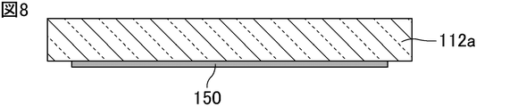
- FIG. 8 is a schematic cross-sectional view showing an example of a step of forming a conductor layer on one surface of a second thermoplastic resin sheet with respect to the method for manufacturing a laminated substrate according to the first embodiment of the present invention.
- the conductor layer 150 is formed on one surface of the second thermoplastic resin sheet 112a.
- the second thermoplastic resin sheet 112a serves as the second thermoplastic resin layer 12a.
- the conductor layer 150 is a second conductor pattern 50.
- the conductor layer 150 As a method of forming the conductor layer 150 on one surface of the second thermoplastic resin sheet 112a, for example, a method of etching the conductor foil attached to one surface of the second thermoplastic resin sheet 112a, the conductor layer 150. Examples thereof include a method of transferring the conductor foil formed in the pattern to one surface of the second thermoplastic resin sheet 112a. As such a conductor foil, it is preferable to use the same conductor foil as described in the step of forming the conductor layer on one surface of the first thermoplastic resin sheet.
- the temperature of the second thermoplastic resin sheet 112a is equal to or higher than the minimum melting point of the melting point of the metal element contained in the conductive paste 190 and lower than the melting point of the first thermoplastic resin sheet 111a and the second thermoplastic resin sheet 112a.
- a thermoplastic resin sheet having a storage elasticity higher than that of the first thermoplastic resin sheet 111a is used.
- the storage elastic modulus of the first thermoplastic resin layer 11a is lower than the storage elastic modulus of the second thermoplastic resin layer 12a at the above-mentioned measured temperature.
- thermoplastic resin constituting the second thermoplastic resin sheet 112a examples include a liquid crystal polymer, a fluororesin, a thermoplastic polyimide resin, a polyether ether ketone resin, and a polyphenylene sulfide resin.
- the second thermoplastic resin sheet 112a may contain a liquid crystal polymer as a main component.
- the storage elastic modulus of the second thermoplastic resin sheet 112a can be adjusted by changing the molecular weight of the liquid crystal polymer, and as described above, the storage elastic modulus of the second thermoplastic resin sheet 112a can be adjusted to the storage elastic modulus of the first thermoplastic resin. It can be higher than the storage elastic modulus of the sheet 111a.
- the thickness of the second thermoplastic resin sheet 112a is, for example, 10 ⁇ m or more and 2000 ⁇ m or less.
- FIG. 9 is a schematic cross-sectional view showing an example of a via hole forming step in a second thermoplastic resin sheet for the method for manufacturing a laminated substrate according to the first embodiment of the present invention.
- via holes 182a and via holes 182b are formed so as to penetrate the second thermoplastic resin sheet 112a, respectively. As a result, a part of the conductor layer 150 and another part are exposed.
- a via hole that exposes still another part of the conductor layer 150 and another part of the conductor layer 150 that penetrate the second thermoplastic resin sheet 112a are formed. Further forms an exposed via hole.
- Examples of the method of forming each via hole in the second thermoplastic resin sheet 112a include a method of irradiating a laser from the other side facing one side of the second thermoplastic resin sheet 112a.
- Such laser irradiation is performed by, for example, a pulse oscillation type carbon dioxide laser irradiation device.
- it is preferable to perform desmear treatment by, for example, oxygen plasma discharge treatment, corona discharge treatment, or the like in order to remove the resin residue.
- the resin residue may be removed by treatment with potassium permanganate or the like.
- each via hole preferably has a tapered shape whose diameter decreases toward the conductor layer 150 formed on one surface of the second thermoplastic resin sheet 112a.
- FIG. 10 is a schematic cross-sectional view showing an example of a step of filling a via hole of a second thermoplastic resin sheet with a conductive paste for the method of manufacturing a laminated substrate according to the first embodiment of the present invention.
- each of the via hole 182a and the via hole 182b is filled with the conductive paste 190.
- the conductive paste 190 filled in the second thermoplastic resin sheet 112a serves as a second interlayer connecting conductor such as the second interlayer connecting conductor 42a.
- Examples of the method of filling each via hole formed in the second thermoplastic resin sheet 112a with the conductive paste 190 include a screen printing method and a vacuum filling method.
- thermoplastic resin sheet 112a filled with the conductive paste 190 and having the conductor layer 150 formed on one surface is produced.
- the second thermoplastic resin sheet 112a formed on the direction may be manufactured at the same timing or at different timings.
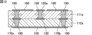
- 11 and 12 are schematic cross-sectional views showing an example of a step of laminating and thermocompression bonding a first thermoplastic resin sheet and a second thermoplastic resin sheet for the method for manufacturing a laminated substrate according to the first embodiment of the present invention.
- the conductive paste 190 is filled, and the first thermoplastic resin sheet 111a in which each conductor layer is formed on one surface and the other surface, and the conductive paste 190 are filled. Further, the second thermoplastic resin sheet 112a in which the conductor layer 150 is formed on one surface is brought into contact with one surface of the first thermoplastic resin sheet 111a and the other surface of the second thermoplastic resin sheet 112a. Laminate in the stacking direction.
- the conductor layer 130 is in contact with both the first thermoplastic resin sheet 111a and the second thermoplastic resin sheet 112a, but the conductor. Since one surface of the layer 130 is exposed from the via hole formed in the first thermoplastic resin sheet 111a, the contact area between the conductor layer 130 and the second thermoplastic resin sheet 112a is the conductor layer 130 and the first thermoplastic. It is larger than the contact area with the resin sheet 111a.
- the laminate of the first thermoplastic resin sheet 111a and the second thermoplastic resin sheet 112a is placed at a temperature equal to or higher than the minimum melting point of the metal elements contained in the conductive paste 190 and is at least the minimum melting point of the first thermoplastic resin sheet 111a.
- the temperature is set to be equal to or lower than the melting point of the second thermoplastic resin sheet 112a.
- the conductive paste 190 is fluidized.
- the first thermoplastic resin sheet 111a and the second thermoplastic are applied by applying pressure to the laminated body of the first thermoplastic resin sheet 111a and the second thermoplastic resin sheet 112a in the laminating direction. It is thermally pressure-bonded to the resin sheet 112a.
- the first thermoplastic resin sheet 111a and the second thermoplastic resin sheet 112a become the first thermoplastic resin layer 11a and the second thermoplastic resin layer 12a, respectively. Since the first thermoplastic resin sheet 111a and the second thermoplastic resin sheet 112a are made of a thermoplastic resin, the first thermoplastic resin layer 11a and the second thermoplastic resin layer 12a are adhered to each other by thermal pressure bonding. become.
- the storage elastic modulus of the first thermoplastic resin sheet 111a at the above temperature is lower than that of the second thermoplastic resin sheet 112a, the pressure applied in the laminating direction during thermal pressure bonding is in the laminating direction as shown by the arrow shown in FIG. It is easy to be converted into pressure in the direction orthogonal to. As a result, as shown in FIG. 12, the conductive paste 190 filled in the first thermoplastic resin sheet 111a is densified while being deformed by the pressure in the direction orthogonal to the laminating direction.
- the conductive paste 190 filled in the first thermoplastic resin sheet 111a is sintered in such a state and has high density, respectively, of the first interlayer connection conductor 41a, the first interlayer connection conductor 41b, and the first interlayer connection conductor 41b.
- the storage elasticity at the above temperature is higher than that of the first thermoplastic resin sheet 111a, so that the pressure applied in the stacking direction is higher than that of the first thermoplastic resin sheet 111a. It is difficult to convert to pressure in the direction orthogonal to the direction. Therefore, as shown in FIG. 12, the conductive paste 190 filled in the second thermoplastic resin sheet 112a is less likely to be deformed than the conductive paste 190 filled in the first thermoplastic resin sheet 111a.
- the conductive paste 190 filled in the second thermoplastic resin sheet 112a is sintered in such a state to form a second interlayer connecting conductor 42a, a second interlayer connecting conductor 42b, a second interlayer connecting conductor 42c, and a second interlayer connecting conductor 42c. , The second interlayer connecting conductor 42d.
- each conductor layer such as the conductor layer 130 formed on one surface of the first thermoplastic resin sheet 111a has the first conductor pattern 30, the connecting conductor layer 70a, the connecting conductor layer 70b, and the connecting conductor layer 70c. And, it becomes the connecting conductor layer 70d.
- the conductor layer 130 is in contact with the second thermoplastic resin sheet 112a having a storage elastic modulus at the above temperature higher than that of the first thermoplastic resin sheet 111a in a large contact area, the conductor layer 130 is thermally generated.
- the first conductor pattern 30 is formed while being less likely to be deformed during crimping and further being less likely to change in position.
- the first conductor pattern 30 is connected to the first interlayer connecting conductor 41a and the first interlayer connecting conductor 41b, which have high density, respectively, while suppressing the deformation and the positional fluctuation.
- the connectivity between the 1 conductor pattern 30 and the first interlayer connection conductor 41a and the connectivity between the first conductor pattern 30 and the first interlayer connection conductor 41b are excellent.
- Each conductor layer such as the conductor layer 120a formed on the other surface of the first thermoplastic resin sheet 111a becomes a surface electrode 20a, a surface electrode 20b, and a ground electrode 60 by this step.
- the conductor layer 150 formed on one surface of the second thermoplastic resin sheet 112a becomes the second conductor pattern 50 by this step.
- the laminated substrate 1 shown in FIGS. 1, 2, and 3 is manufactured.
- the first interlayer connection conductor 41a is sintered while the conductive paste 190 is deformed and densified by the pressure in the direction orthogonal to the laminating direction in the manufacturing process of the laminated substrate 1. Therefore, the first interlayer connection conductor 41a tends to have a constricted shape as shown in FIGS. 1, 2, and 3. More specifically, the first interlayer connection conductor 41a has a cross-sectional area of an end portion on the first conductor pattern 30 side and a breakage of the end portion on the opposite side to the first conductor pattern 30 in a cross section orthogonal to the stacking direction. It tends to have a shape that has a cross-sectional area smaller than both of the areas.
- the stress applied to the first interlayer connection conductor 41a is relaxed, so that the connectivity between the first conductor pattern 30 and the first interlayer connection conductor 41a is further improved.
- the first interlayer connection conductor 41a has such a constricted shape, the cross-sectional area of the end portion of the first interlayer connection conductor 41a on the first conductor pattern 30 side tends to be large, so more specifically. Since the contact area between the first interlayer connection conductor 41a and the first conductor pattern 30 tends to be large, the connectivity between the first conductor pattern 30 and the first interlayer connection conductor 41a is further improved.
- the first interlayer connection conductor 41b is sintered while the conductive paste 190 is deformed and densified by the pressure in the direction orthogonal to the laminating direction in the manufacturing process of the laminated substrate 1. Therefore, the first interlayer connection conductor 41b tends to have a constricted shape as shown in FIGS. 1 and 3. More specifically, the first interlayer connection conductor 41b has a cross-sectional area of an end portion on the first conductor pattern 30 side and a breakage of the end portion on the opposite side to the first conductor pattern 30 in a cross section orthogonal to the stacking direction. It tends to have a shape that has a cross-sectional area smaller than both of the areas.
- the stress applied to the first interlayer connection conductor 41b is relaxed, so that the connectivity between the first conductor pattern 30 and the first interlayer connection conductor 41b becomes even better.
- the first interlayer connecting conductor 41b has such a constricted shape, the cross-sectional area of the end portion of the first interlayer connecting conductor 41b on the first conductor pattern 30 side tends to be large, so more specifically. Since the contact area between the first interlayer connection conductor 41b and the first conductor pattern 30 tends to be large, the connectivity between the first conductor pattern 30 and the first interlayer connection conductor 41b becomes even better.
- the third interlayer connection conductor 43a, the third interlayer connection conductor 43b, the third interlayer connection conductor 43c, and the third interlayer connection conductor 43d are also constricted in the same manner as the first interlayer connection conductor 41a and the first interlayer connection conductor 41b. It tends to have a different shape.
- the second interlayer connection conductor 42a, the second interlayer connection conductor 42b, the second interlayer connection conductor 42c, and the second interlayer connection conductor 42d, respectively, remain that the conductive paste 190 is not easily deformed in the manufacturing process of the laminated substrate 1. It is sintered. That is, the second interlayer connecting conductor 42a, the second interlayer connecting conductor 42b, the second interlayer connecting conductor 42c, and the second interlayer connecting conductor 42d each have the same shape as each via hole filled with the conductive paste 190. Here, it tends to have a tapered shape.
- the ends of the second interlayer connecting conductor 42a, the second interlayer connecting conductor 42b, the second interlayer connecting conductor 42c, and the second interlayer connecting conductor 42d on the second conductor pattern 50 side tends to be smaller than the cross-sectional area of the ends of the first interlayer connecting conductor 41a and the first interlayer connecting conductor 41b on the first conductor pattern 30 side.
- the void ratio of the first interlayer connecting conductor 41a and the first interlayer connecting conductor 41b is the second interlayer connecting conductor 42a, the second interlayer connecting conductor 42b, the second interlayer connecting conductor 42c, and the second interlayer. It tends to be lower than the void ratio of the connecting conductor 42d.
- the comparison of the void ratios of the interlayer connecting conductors is performed by observing the cross section along the stacking direction as shown in FIGS. 2 and 3 with a scanning electron microscope (SEM).
- the dielectric loss tangent of the second thermoplastic resin layer 12a is smaller than the dielectric loss tangent of the first thermoplastic resin layer 11a.
- the first conductor pattern 30 has a large length in the transmission direction orthogonal to the stacking direction, it tends to affect the loss of electrical energy (for example, the generation of leakage current).
- the area where the first conductor pattern 30 and the second conductor pattern 50 face each other via the second thermoplastic resin layer 12a is such that the first conductor pattern 30 and the ground electrode 60 pass through the first thermoplastic resin layer 11a. Since it is larger than the facing area, the loss of electric energy tends to be larger between the first conductor pattern 30 and the second conductor pattern 50.
- the dielectric loss tangent of the second thermoplastic resin layer 12a smaller than the dielectric loss tangent of the first thermoplastic resin layer 11a, the above-mentioned loss of electrical energy can be reduced.
- the first thermoplastic resin layer may be composed of a plurality of first thermoplastic sub-resin layers.
- An example of such a laminated substrate of the present invention will be described below as a laminated substrate of a modified example of the first embodiment of the present invention.
- the laminated substrate of the modified example of the first embodiment of the present invention is the same as the laminated substrate of the first embodiment of the present invention except for the configuration of the first thermoplastic resin layer.
- FIG. 13 is a schematic cross-sectional view showing a laminated substrate of a modified example of the first embodiment of the present invention.
- FIG. 13 shows a cross section corresponding to FIG.
- the first thermoplastic resin layer 11a is composed of the first thermoplastic sub-resin layer 11aa and the first thermoplastic sub-resin layer 11ab. More specifically, in the first thermoplastic resin layer 11a, the first thermoplastic sub-resin layer 11ab and the first thermoplastic sub-resin adjacent to the first thermoplastic sub-resin layer 11ab are in this order from the second laminated portion 12 side. A resin layer 11aa is provided.
- the melting point of the metal element contained in the first interlayer connecting conductor 41a and the first interlayer connecting conductor 41b is equal to or higher than the minimum melting point, and the first thermoplastic resin layer 11a and the second thermoplastic resin layer 12a are formed.
- the storage elastic modulus of the first thermoplastic resin layer 11a is lower than the storage elastic modulus of the second thermoplastic resin layer 12a.
- the first thermoplastic secondary resin layer 11aa and The storage elastic modulus of the first thermoplastic auxiliary resin layer 11ab may be lower than the storage elastic modulus of the second thermoplastic resin layer 12a, or the first thermoplastic auxiliary resin layer 11aa and the first thermoplastic auxiliary resin.
- the storage elastic modulus of one of the layers 11ab may be the same as the storage elastic modulus of the second thermoplastic resin layer 12a.
- the first thermoplastic subresin layer 11aa and the first thermoplastic subresin layer 11ab When the storage elasticity of the first thermoplastic subresin layer 11aa and the first thermoplastic subresin layer 11ab is lower than the storage elasticity of the second thermoplastic resin layer 12a at the above measurement temperature, the first thermoplastic subresin layer The storage elasticity of 11aa and the first thermoplastic subresin layer 11ab may be the same as or different from each other.
- the first thermoplastic subresin layer 11aa contains a liquid crystal polymer as a main component.
- the first thermoplastic auxiliary resin layer 11ab may contain a fluororesin as a main component.
- the first thermoplastic sub-resin layer 11aa may contain a fluororesin as a main component
- the first thermoplastic sub-resin layer 11ab may contain a liquid crystal polymer as a main component.
- the fluororesin is a resin having a relatively low storage elasticity among the above-mentioned examples of the thermoplastic resin
- the first thermoplastic subresin layer 11aa or the first thermoplastic subresin layer 11ab contains the fluororesin as a main component. If this is the case, the overall storage elasticity of the first thermoplastic resin layer 11a at the measured temperature tends to be low.
- the dielectric loss tangent of the first thermoplastic sub-resin layer 11ab provided in contact with the first conductor pattern 30 is preferably lower than the dielectric loss tangent of the first thermoplastic sub-resin layer 11aa.
- the first thermoplastic sub-resin layer having the smallest dielectric loss tangent is preferably provided so as to be in contact with the first conductor pattern 30. This makes it possible to reduce the loss of electrical energy in the first conductor pattern 30.
- the first thermoplastic resin layer 11a is composed of two first thermoplastic sub-resin layers, but may be composed of three or more first thermoplastic sub-resin layers.
- the storage elastic modulus of the first thermoplastic resin layer 11a as a whole at the above-mentioned measurement temperature is the second thermoplastic resin layer 12a.
- the storage elastic modulus of these first thermoplastic subresin layers may be lower than the storage elastic modulus of the second thermoplastic resin layer 12a, if it is lower than the storage elastic modulus of the first thermoplastic resin layer.
- the storage elastic modulus of a part of the plastic subresin layer may be the same as the storage elastic modulus of the second thermoplastic resin layer 12a.
- the storage elastic modulus of these first thermoplastic auxiliary resin layers is determined. They may be the same as each other or different from each other. Further, from the viewpoint of reducing the loss of electrical energy in the first conductor pattern 30, among these first thermoplastic sub-resin layers, the first thermoplastic sub-resin layer having the smallest dielectric loss tangent is the first conductor pattern. It is preferable that it is provided so as to be in contact with 30.
- the second thermoplastic resin layer 12a is composed of one layer, but it may be composed of a plurality of second thermoplastic secondary resin layers.
- thermoplastic resin layer 11a is composed of a plurality of first thermoplastic sub-resin layers and the second thermoplastic resin layer 12a is composed of a plurality of second thermoplastic sub-resin layers
- the maximum value of the storage elasticity of the first thermoplastic subresin layer of the plurality of layers may be lower than the minimum value of the storage elasticity of the second thermoplastic subresin layer of the plurality of layers.
- the storage elastic modulus of the second thermoplastic subresin layer of the plurality of layers may be the same as or different from each other as long as it is higher than the maximum value of the storage elastic modulus of the first thermoplastic subresin layer of the plurality of layers. May be.
- thermoplastic resin layer 11a is composed of a plurality of first thermoplastic subresin layers
- second thermoplastic resin layer 12a is composed of a plurality of second thermoplastic subresin layers.
- the temperature dependence of the storage elasticity of the thermoplastic resin layer as a whole is measured by dynamic viscoelasticity measurement if the thermoplastic resin layer composed of multiple layers is used as the measurement sample. can.
- the first laminated portion may be composed of a plurality of first thermoplastic resin layers, and at least one first interlayer connection is connected to each of the plurality of first thermoplastic resin layers.
- a conductor may be provided.
- An example of such a laminated substrate of the present invention will be described below as the laminated substrate of the second embodiment of the present invention.
- the laminated substrate of the second embodiment of the present invention is the same as the laminated substrate of the first embodiment of the present invention except for the configuration of the resin laminate.
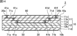
- FIG. 14 is a schematic cross-sectional view showing the laminated substrate of the second embodiment of the present invention.
- FIG. 14 shows a cross section corresponding to FIG.
- the first laminated portion 11 is composed of a first thermoplastic resin layer 11a, a first thermoplastic resin layer 11b, and a first thermoplastic resin layer 11c.
- the first thermoplastic resin layer 11a, the first thermoplastic resin layer 11b adjacent to the first thermoplastic resin layer 11a, and the first thermoplastic resin layer are in this order from the second laminated portion 12 side.
- a first thermoplastic resin layer 11c adjacent to 11b is provided.
- the same type of first thermoplastic resin layer such as the first thermoplastic resin layer 11a, the first thermoplastic resin layer 11b, and the first thermoplastic resin layer 11c is laminated in the stacking direction. Since it is laminated in, the adhesion between the first thermoplastic resin layers is high.
- the first thermoplastic resin layer 11a is provided with a first interlayer connection conductor 41a and a first interlayer connection conductor 41b that penetrate in the stacking direction at separate positions.
- the first thermoplastic resin layer 11b is provided with a first interlayer connecting conductor 41c and a first interlayer connecting conductor 41d that penetrate in the stacking direction at separate positions.
- the first thermoplastic resin layer 11c is provided with a first interlayer connecting conductor 41e and a first interlayer connecting conductor 41f that penetrate in the stacking direction at positions separated from each other.
- the lengths of the first interlayer connecting conductor 41c, the first interlayer connecting conductor 41d, the first interlayer connecting conductor 41e, and the first interlayer connecting conductor 41f are the lengths of the first interlayer connecting conductor, respectively. Similar to the length of 41a and the first interlayer connection conductor 41b, it is smaller than the length of the first conductor pattern 30.
- the first interlayer connection conductor 41c, the first interlayer connection conductor 41d, the first interlayer connection conductor 41e, and the first interlayer connection conductor 41f are similar to the first interlayer connection conductor 41a and the first interlayer connection conductor 41b, respectively. It contains a resin and at least one metal element.
- the resins contained in the first interlayer connection conductor 41a, the first interlayer connection conductor 41b, the first interlayer connection conductor 41c, the first interlayer connection conductor 41d, the first interlayer connection conductor 41e, and the first interlayer connection conductor 41f are mutual. It is preferably the same, but may be different from each other. Further, metal elements contained in the first interlayer connection conductor 41a, the first interlayer connection conductor 41b, the first interlayer connection conductor 41c, the first interlayer connection conductor 41d, the first interlayer connection conductor 41e, and the first interlayer connection conductor 41f. Are preferably the same as each other, but may be different from each other.
- first interlayer connection conductor 41a, the first interlayer connection conductor 41b, the first interlayer connection conductor 41c, the first interlayer connection conductor 41d, the first interlayer connection conductor 41e, and the first interlayer connection conductor 41f are made of the same resin. And preferably contain the same metal elements as each other.
- the laminated substrate 2 may further have a connecting conductor layer 71a, a connecting conductor layer 71b, a connecting conductor layer 71c, and a connecting conductor layer 71d.
- the connecting conductor layer 71a is provided between the first thermoplastic resin layer 11a and the first thermoplastic resin layer 11b.
- the connecting conductor layer 71a is preferably provided so as to straddle the boundary between the first thermoplastic resin layer 11a and the first thermoplastic resin layer 11b.
- the interface between the connecting conductor layer 71a and the first thermoplastic resin layer 11a and the interface between the connecting conductor layer 71a and the first thermoplastic resin layer 11b become the first thermoplastic resin layer 11a and the first thermoplastic.
- the connecting conductor layer 71a electrically connects the first interlayer connecting conductor 41a and the first interlayer connecting conductor 41c.
- the connecting conductor layer 71b is provided between the first thermoplastic resin layer 11a and the first thermoplastic resin layer 11b at a position separated from the connecting conductor layer 71a.
- the connecting conductor layer 71a is preferably provided at a position separated from the connecting conductor layer 71a across the boundary between the first thermoplastic resin layer 11a and the first thermoplastic resin layer 11b.
- the connecting conductor layer 71b electrically connects the first interlayer connecting conductor 41b and the first interlayer connecting conductor 41d.
- the connecting conductor layer 71c is provided between the first thermoplastic resin layer 11b and the first thermoplastic resin layer 11c.
- the connecting conductor layer 71c is preferably provided so as to straddle the boundary between the first thermoplastic resin layer 11b and the first thermoplastic resin layer 11c.
- the interface between the connecting conductor layer 71c and the first thermoplastic resin layer 11b and the interface between the connecting conductor layer 71c and the first thermoplastic resin layer 11c become the first thermoplastic resin layer 11b and the first thermoplastic.
- the connecting conductor layer 71c electrically connects the first interlayer connecting conductor 41c and the first interlayer connecting conductor 41e.
- the connecting conductor layer 71d is provided between the first thermoplastic resin layer 11b and the first thermoplastic resin layer 11c at a position separated from the connecting conductor layer 71c.
- the connecting conductor layer 71d is preferably provided at a position separated from the connecting conductor layer 71c across the boundary between the first thermoplastic resin layer 11b and the first thermoplastic resin layer 11c.
- the connecting conductor layer 71d electrically connects the first interlayer connecting conductor 41d and the first interlayer connecting conductor 41f.
- the lengths of the connecting conductor layer 71a, the connecting conductor layer 71b, the connecting conductor layer 71c, and the connecting conductor layer 71d are the connecting conductor layer 70a, the connecting conductor layer 70b, and the connecting conductor layer, respectively. Similar to the length of 70c and the connecting conductor layer 70d, it is smaller than the length of the first conductor pattern 30.
- the constituent materials of the connecting conductor layer 71a, the connecting conductor layer 71b, the connecting conductor layer 71c, and the connecting conductor layer 71d include, for example, the connecting conductor layer 70a, the connecting conductor layer 70b, the connecting conductor layer 70c, and the connecting conductor layer 70d.
- the same as the constituent materials of the above can be mentioned.
- the constituent materials of the connecting conductor layer 71a, the connecting conductor layer 71b, the connecting conductor layer 71c, and the connecting conductor layer 71d are preferably the same as each other, but may be different from each other.
- the first laminated portion 11 is composed of three layers of the first thermoplastic resin layer, but may be composed of two layers of the first thermoplastic resin layer, or may be composed of two or more first thermoplastic resin layers. It may consist of a thermoplastic resin layer.
- the second laminated portion 12 may be composed of a plurality of layers of the second thermoplastic resin layer.
- the second laminated portion 12 may be composed of the second thermoplastic resin layer 12a and the second thermoplastic resin layer 12b.
- a second thermoplastic resin layer 12a and a second thermoplastic resin layer 12b adjacent to the second thermoplastic resin layer 12a are provided in this order from the first laminated portion 11 side.
- the same kind of second thermoplastic resin layer such as the second thermoplastic resin layer 12a and the second thermoplastic resin layer 12b is laminated in the laminating direction, so that each second is laminated. 2 High adhesion between thermoplastic resin layers.
- the boundary between the first thermoplastic resin layers of the same type such as the first thermoplastic resin layer 11a, the first thermoplastic resin layer 11b, and the first thermoplastic resin layer 11c, and the second thermoplastic resin there is a boundary between layers of the same type of second thermoplastic resin such as the layer 12a and the second thermoplastic resin layer 12b, but even at such a boundary, with respect to a cross section along the stacking direction as shown in FIG. As described above, it can be determined by observing by infrared spectroscopy or by observing the position of the end portion of each interlayer connection conductor.
- the first interlayer connecting conductor is used. All constituting the first laminated portion at a measurement temperature equal to or higher than the minimum melting point of the melting points of the contained metal elements and lower than the melting point of the plurality of layers of the first thermoplastic resin layer and the plurality of layers of the second thermoplastic resin layer.
- the storage elasticity of the first thermoplastic resin layer is lower than the storage elasticity of all the second thermoplastic resin layers constituting the second laminated portion.
- the first interlayer connection conductor 41a the first interlayer connection conductor 41b, the first interlayer connection conductor 41c, the first interlayer connection conductor 41d, the first interlayer connection conductor 41e, and the first interlayer connection conductor 41f.
- 1st thermoplastic resin layer 11a, 1st thermoplastic resin layer 11b, 1st thermoplastic resin layer 11c, 2nd thermoplastic resin layer 12a, and 2nd At the measurement temperature below the melting point of the thermoplastic resin layer 12b, the storage elasticity of the first thermoplastic resin layer 11a, the first thermoplastic resin layer 11b, and the first thermoplastic resin layer 11c is the second thermoplastic resin layer. It is lower than the storage elasticity of 12a and the second thermoplastic resin layer 12b.
- the first interlayer connection conductor 41a, the first interlayer connection conductor 41b, the first interlayer connection conductor 41c, the first interlayer connection conductor 41d, the first interlayer connection conductor 41e, and the first interlayer connection conductor 41f are respectively. It will have high precision.
- the surface electrode 20a and the first conductor pattern 30 form a first interlayer connection conductor 41a, a connection conductor layer 71a, a first interlayer connection conductor 41c, a connection conductor layer 71c, and a first interlayer connection conductor 41e. It is electrically connected via.
- the first interlayer connection conductor that electrically connects the surface electrode 20a and the first conductor pattern 30 has high density, respectively, and the first interlayer connection conductor 41a and the first interlayer connection are connected. Since the conductor 41c and the first interlayer connection conductor 41e, the connectivity between the surface electrode 20a and the first conductor pattern 30 tends to be improved.
- the first interlayer connection conductor 41a, the first interlayer connection conductor 41c, and the first interlayer connection conductor 41e are provided so as not to overlap each other when viewed from the stacking direction, but they overlap each other. It may be provided as follows. Alternatively, a first interlayer connecting conductor that electrically connects the surface electrode 20a and the first conductor pattern 30 may be provided so as to penetrate two or more layers of the first thermoplastic resin layer.
- the surface electrode 20b and the first conductor pattern 30 form a first interlayer connection conductor 41b, a connection conductor layer 71b, a first interlayer connection conductor 41d, a connection conductor layer 71d, and a first interlayer connection conductor 41f. It is electrically connected via.
- the first interlayer connection conductor that electrically connects the surface electrode 20b and the first conductor pattern 30 has high density, respectively, and the first interlayer connection conductor 41b and the first interlayer connection are connected. Since the conductor 41d and the first interlayer connection conductor 41f, the connectivity between the surface electrode 20b and the first conductor pattern 30 tends to be improved.
- the first interlayer connection conductor 41b, the first interlayer connection conductor 41d, and the first interlayer connection conductor 41f are provided so as not to overlap each other when viewed from the stacking direction, but they overlap each other. It may be provided as follows. Alternatively, a first interlayer connecting conductor that electrically connects the surface electrode 20b and the first conductor pattern 30 may be provided so as to penetrate two or more layers of the first thermoplastic resin layer.
- the storage elastic moduli of the first thermoplastic resin layer 11a, the first thermoplastic resin layer 11b, and the first thermoplastic resin layer 11c are preferably the same.
- the adhesion between the first thermoplastic resin layer 11a, the first thermoplastic resin layer 11b, and the first thermoplastic resin layer 11c is likely to increase.
- the thermoplastic resins constituting the first thermoplastic resin layer 11a, the first thermoplastic resin layer 11b, and the first thermoplastic resin layer 11c are preferably the same, but may be different from each other. good.
- the storage elastic moduli of the first thermoplastic resin layer 11a, the first thermoplastic resin layer 11b, and the first thermoplastic resin layer 11c may be different from each other.
- the thermoplastic resins constituting the first thermoplastic resin layer 11a, the first thermoplastic resin layer 11b, and the first thermoplastic resin layer 11c may be the same or different from each other. good.
- the storage elastic moduli of the second thermoplastic resin layer 12a and the second thermoplastic resin layer 12b may be the same as each other or may be different from each other.
- the thermoplastic resins constituting the second thermoplastic resin layer 12a and the second thermoplastic resin layer 12b may be the same as each other or may be different from each other.
- the thermoplastic resins constituting the second thermoplastic resin layer 12a and the second thermoplastic resin layer 12b are the first thermoplastic resin layer 11a, the first thermoplastic resin layer 11b, and the first thermoplastic resin layer 11c. It may be the same as or different from the thermoplastic resin constituting the above.
- the first thermoplastic resin layer 11a, the first thermoplastic resin layer 11b, the first thermoplastic resin layer 11c, the second thermoplastic resin layer 12a, and the second thermoplastic resin layer 12b each contain a liquid crystal polymer as a main component. May be included as.
- the molecular weights of the liquid crystal polymers constituting the first thermoplastic resin layer 11a, the first thermoplastic resin layer 11b, and the first thermoplastic resin layer 11c, and the second thermoplastic resin layer 12a and the second thermoplastic resin It is preferable that the molecular weights of the liquid crystal polymers constituting the layer 12b are different from each other.
- the storage elasticity of the first thermoplastic resin layer 11a, the first thermoplastic resin layer 11b, and the first thermoplastic resin layer 11c is adjusted to the second thermoplastic resin layer 12a and the second thermoplastic resin layer 12b. It can be lower than the storage elasticity.
- the resin laminated body 10 may further have at least one first thermoplastic resin layer on the side opposite to the first laminated portion 11 with respect to the second laminated portion 12.
- the resin laminated body 10 may further have a first thermoplastic resin layer 11d on the side opposite to the first laminated portion 11 with respect to the second laminated portion 12.
- the impedance of the laminated substrate 2 can be appropriately adjusted.
- the first interlayer connecting conductor 41a, the first interlayer connecting conductor 41b, the first interlayer connecting conductor 41c, the first interlayer connecting conductor 41d, and the first The minimum melting point of the metal elements contained in the one interlayer connecting conductor 41e and the first interlayer connecting conductor 41f is equal to or higher than the minimum melting point
- the first thermoplastic resin layer 11d, the second thermoplastic resin layer 12a, and the second At a measurement temperature below the melting point of the thermoplastic resin layer 12b, the storage elasticity of the first thermoplastic resin layer 11d is lower than the storage elasticity of the second thermoplastic resin layer 12a and the second thermoplastic resin layer 12b.
- the resin laminate 10 has the first thermoplastic resin layer 11d, the first interlayer connecting conductor 41a, the first interlayer connecting conductor 41b, the first interlayer connecting conductor 41c, and the first interlayer connecting conductor 41d.
- the first thermoplastic resin layer 11a and the first heat at the measurement temperature below the melting point of the thermoplastic resin layer 11c, the first thermoplastic resin layer 11d, the second thermoplastic resin layer 12a, and the second thermoplastic resin layer 12b.
- the storage elasticity of the plastic resin layer 11b, the first thermoplastic resin layer 11c, and the first thermoplastic resin layer 11d is lower than the storage elasticity of the second thermoplastic resin layer 12a and the second thermoplastic resin layer 12b. Is preferable.
- the storage elastic modulus of the first thermoplastic resin layer 11d is the first thermoplastic resin layer 11a, the first thermoplastic resin layer 11b, and the first thermoplastic resin at any of the above-mentioned measurement temperatures. It may be the same as or different from the storage elastic modulus of the layer 11c.
- the thermoplastic resin constituting the first thermoplastic resin layer 11d is the heat constituting the first thermoplastic resin layer 11a, the first thermoplastic resin layer 11b, and the first thermoplastic resin layer 11c. It may be the same as or different from the plastic resin.
- a plurality of first conductor patterns 30 exist, and all the first conductor patterns 30 have a first interlayer connection conductor on a surface electrode provided on the first main surface 10a of the resin laminate 10.
- all the first conductor patterns 30 are preferably provided so as to be in contact with the first thermoplastic resin layer of the first laminated portion 11.
- the length of the first conductor pattern 30 of the lowest layer that is, the first conductor pattern 30 provided between the first laminated portion 11 and the second laminated portion 12.
Landscapes
- Engineering & Computer Science (AREA)
- Microelectronics & Electronic Packaging (AREA)
- Manufacturing & Machinery (AREA)
- Production Of Multi-Layered Print Wiring Board (AREA)
Abstract
Description
図1は、本発明の実施形態1の積層基板を示す分解斜視模式図である。図2は、図1中の線分A1-A2に対応する部分を示す断面模式図である。図3は、図1中の線分B1-B2に対応する部分を示す断面模式図である。
図4は、本発明の実施形態1の積層基板の製造方法について、第1熱可塑性樹脂シートの一方面への導体層形成工程の一例を示す断面模式図である。
図5は、本発明の実施形態1の積層基板の製造方法について、第1熱可塑性樹脂シートへのビアホール形成工程の一例を示す断面模式図である。
図6は、本発明の実施形態1の積層基板の製造方法について、第1熱可塑性樹脂シートのビアホールへの導電性ペースト充填工程の一例を示す断面模式図である。
図7は、本発明の実施形態1の積層基板の製造方法について、第1熱可塑性樹脂シートの他方面への導体層形成工程の一例を示す断面模式図である。
図8は、本発明の実施形態1の積層基板の製造方法について、第2熱可塑性樹脂シートの一方面への導体層形成工程の一例を示す断面模式図である。
図9は、本発明の実施形態1の積層基板の製造方法について、第2熱可塑性樹脂シートへのビアホール形成工程の一例を示す断面模式図である。
図10は、本発明の実施形態1の積層基板の製造方法について、第2熱可塑性樹脂シートのビアホールへの導電性ペースト充填工程の一例を示す断面模式図である。
図11及び図12は、本発明の実施形態1の積層基板の製造方法について、第1熱可塑性樹脂シート及び第2熱可塑性樹脂シートの積層・熱圧着工程の一例を示す断面模式図である。
本発明の実施形態1の積層基板において、第1熱可塑性樹脂層は、複数層の第1熱可塑性副樹脂層からなっていてもよい。このような本発明の積層基板の一例を、本発明の実施形態1の変形例の積層基板として以下に説明する。本発明の実施形態1の変形例の積層基板は、第1熱可塑性樹脂層の構成以外、本発明の実施形態1の積層基板と同様である。
本発明の積層基板において、第1積層部は、複数層の第1熱可塑性樹脂層からなっていてもよく、複数層の第1熱可塑性樹脂層には、各々、少なくとも1つの第1層間接続導体が設けられていてもよい。このような本発明の積層基板の一例を、本発明の実施形態2の積層基板として以下に説明する。本発明の実施形態2の積層基板は、樹脂積層体の構成以外、本発明の実施形態1の積層基板と同様である。
10 樹脂積層体
10a 第1主面
10b 第2主面
11 第1積層部
11a、11b、11c、11d 第1熱可塑性樹脂層
11aa、11ab 第1熱可塑性副樹脂層
12 第2積層部
12a、12b 第2熱可塑性樹脂層
20a、20b 表面電極
30 信号用又は電力伝送用の第1導体パターン
41a、41b、41c、41d、41e、41f 第1層間接続導体
42a、42b、42c、42d 第2層間接続導体
43a、43b、43c、43d 第3層間接続導体
50 グランド用の第2導体パターン
60 グランド電極
70a、70b、70c、70d、71a、71b、71c、71d 接続導体層
111a 第1熱可塑性樹脂シート
112a 第2熱可塑性樹脂シート
120a、130、150、160、170a、170b 導体層
181a、182a、182b、183a、183b ビアホール
190 導電性ペースト
Claims (13)
- 少なくとも1層の第1熱可塑性樹脂層からなる第1積層部と、前記第1積層部に隣接し、少なくとも1層の第2熱可塑性樹脂層からなる第2積層部とを積層方向に含む積層構造を有し、かつ、前記積層方向に対向する、前記第1積層部側の第1主面及び前記第2積層部側の第2主面を有する樹脂積層体と、
前記樹脂積層体の前記第1主面上に設けられた表面電極と、
前記第1積層部と前記第2積層部との間に設けられた信号用又は電力伝送用の第1導体パターンと、
前記第1熱可塑性樹脂層を前記積層方向に貫通するように設けられ、かつ、前記表面電極と前記第1導体パターンとを電気的に接続する少なくとも1つの第1層間接続導体と、を備え、
前記第1導体パターンでは、前記積層方向において、前記表面電極側の一方面が前記第1層間接続導体に接続され、かつ、前記表面電極と反対側の他方面が層間接続導体に接続されず、
前記第1層間接続導体は、樹脂及び少なくとも1種の金属元素を含み、
前記第1層間接続導体に含まれる前記金属元素の融点のうちの最小融点以上、かつ、前記第1熱可塑性樹脂層及び前記第2熱可塑性樹脂層の融点以下の測定温度において、前記第1熱可塑性樹脂層の貯蔵弾性率は、前記第2熱可塑性樹脂層の貯蔵弾性率よりも低い、ことを特徴とする積層基板。 - 前記第1層間接続導体は、前記最小融点を有する前記金属元素として錫を含む、請求項1に記載の積層基板。
- 前記第1層間接続導体は、前記金属元素として銅を含む、請求項1又は2に記載の積層基板。
- 前記第1層間接続導体は、前記積層方向に直交する断面において、前記第1導体パターン側の端部の断面積、及び、前記第1導体パターンと反対側の端部の断面積の両方よりも小さい断面積を有する、請求項1~3のいずれかに記載の積層基板。
- 前記第1導体パターンに対して前記樹脂積層体の前記第2主面側に設けられ、かつ、前記積層方向から見たときに前記第1導体パターンと重なるグランド用の第2導体パターンを更に有する、請求項1~4のいずれかに記載の積層基板。
- 前記積層方向から見たときに前記第1層間接続導体を挟む位置で前記第2熱可塑性樹脂層を前記積層方向に貫通するように設けられ、かつ、前記第2導体パターンに電気的に接続された複数の第2層間接続導体を更に有する、請求項5に記載の積層基板。
- 前記積層方向に直交する断面において、前記第2層間接続導体の前記第2導体パターン側の端部の断面積は、前記第1層間接続導体の前記第1導体パターン側の端部の断面積よりも小さい、請求項6に記載の積層基板。
- 前記第1層間接続導体の空隙率は、前記第2層間接続導体の空隙率よりも低い、請求項6又は7に記載の積層基板。
- 前記第2熱可塑性樹脂層の誘電正接は、前記第1熱可塑性樹脂層の誘電正接よりも小さい、請求項5~8のいずれかに記載の積層基板。
- 前記第1熱可塑性樹脂層及び前記第2熱可塑性樹脂層は、各々、液晶ポリマーを主成分として含む、請求項1~9のいずれかに記載の積層基板。
- 前記第1積層部は、複数層の前記第1熱可塑性樹脂層からなり、
複数層の前記第1熱可塑性樹脂層には、各々、少なくとも1つの前記第1層間接続導体が設けられている、請求項1~10のいずれかに記載の積層基板。 - 前記積層方向に隣接する2層の前記第1熱可塑性樹脂層の間に、各々の前記第1熱可塑性樹脂層に設けられた前記第1層間接続導体同士を電気的に接続する少なくとも1層の接続導体層を更に有し、
前記積層方向に直交する伝送方向において、前記接続導体層の長さは、前記第1導体パターンの長さよりも小さい、請求項11に記載の積層基板。 - 前記測定温度において、複数層の前記第1熱可塑性樹脂層の貯蔵弾性率は、互いに同じである、請求項11又は12に記載の積層基板。
Priority Applications (3)
| Application Number | Priority Date | Filing Date | Title |
|---|---|---|---|
| CN202180044784.6A CN115997484B (zh) | 2020-06-30 | 2021-06-23 | 层叠基板 |
| JP2022533900A JPWO2022004504A1 (ja) | 2020-06-30 | 2021-06-23 | |
| US18/082,619 US12167545B2 (en) | 2020-06-30 | 2022-12-16 | Multilayer substrate |
Applications Claiming Priority (2)
| Application Number | Priority Date | Filing Date | Title |
|---|---|---|---|
| JP2020-113184 | 2020-06-30 | ||
| JP2020113184 | 2020-06-30 |
Related Child Applications (1)
| Application Number | Title | Priority Date | Filing Date |
|---|---|---|---|
| US18/082,619 Continuation US12167545B2 (en) | 2020-06-30 | 2022-12-16 | Multilayer substrate |
Publications (1)
| Publication Number | Publication Date |
|---|---|
| WO2022004504A1 true WO2022004504A1 (ja) | 2022-01-06 |
Family
ID=79316203
Family Applications (1)
| Application Number | Title | Priority Date | Filing Date |
|---|---|---|---|
| PCT/JP2021/023697 Ceased WO2022004504A1 (ja) | 2020-06-30 | 2021-06-23 | 積層基板 |
Country Status (4)
| Country | Link |
|---|---|
| US (1) | US12167545B2 (ja) |
| JP (1) | JPWO2022004504A1 (ja) |
| CN (1) | CN115997484B (ja) |
| WO (1) | WO2022004504A1 (ja) |
Cited By (2)
| Publication number | Priority date | Publication date | Assignee | Title |
|---|---|---|---|---|
| JPWO2024252979A1 (ja) * | 2023-06-06 | 2024-12-12 | ||
| WO2025134699A1 (ja) * | 2023-12-22 | 2025-06-26 | 株式会社村田製作所 | 積層基板 |
Families Citing this family (1)
| Publication number | Priority date | Publication date | Assignee | Title |
|---|---|---|---|---|
| TWI909716B (zh) * | 2024-09-26 | 2025-12-21 | 國立臺灣大學 | 基板間的訊號傳輸電路 |
Citations (4)
| Publication number | Priority date | Publication date | Assignee | Title |
|---|---|---|---|---|
| JP2009065009A (ja) * | 2007-09-07 | 2009-03-26 | Mitsubishi Plastics Inc | 多層配線基板 |
| WO2017081981A1 (ja) * | 2015-11-10 | 2017-05-18 | 株式会社村田製作所 | 樹脂多層基板およびその製造方法 |
| WO2020071473A1 (ja) * | 2018-10-04 | 2020-04-09 | 株式会社村田製作所 | 積層体及びその製造方法 |
| JP2020072198A (ja) * | 2018-10-31 | 2020-05-07 | 日鉄ケミカル&マテリアル株式会社 | 金属張積層板、回路基板、多層回路基板及びその製造方法 |
Family Cites Families (10)
| Publication number | Priority date | Publication date | Assignee | Title |
|---|---|---|---|---|
| US5248530A (en) | 1991-11-27 | 1993-09-28 | Hoechst Celanese Corp. | Heat sealable coextruded lcp film |
| US5719354A (en) | 1994-09-16 | 1998-02-17 | Hoechst Celanese Corp. | Monolithic LCP polymer microelectronic wiring modules |
| JP2005175279A (ja) * | 2003-12-12 | 2005-06-30 | Nippon Mektron Ltd | 多層回路基板とその製造方法 |
| JP2006093439A (ja) * | 2004-09-24 | 2006-04-06 | Denso Corp | 多層基板及びその製造方法 |
| JP5077448B2 (ja) * | 2010-04-02 | 2012-11-21 | 株式会社デンソー | 半導体チップ内蔵配線基板及びその製造方法 |
| JP2015070175A (ja) * | 2013-09-30 | 2015-04-13 | 大日本印刷株式会社 | 配線層の接続構造体 |
| CN106537684B (zh) | 2015-04-09 | 2019-11-01 | 株式会社村田制作所 | 复合传输线路以及电子设备 |
| JP6977716B2 (ja) * | 2016-04-11 | 2021-12-08 | Agc株式会社 | 積層体、プリント基板、および積層体の製造方法 |
| CN109644567A (zh) * | 2016-08-24 | 2019-04-16 | 松下知识产权经营株式会社 | 电路基板的制造方法 |
| JP2021007115A (ja) * | 2017-08-17 | 2021-01-21 | 株式会社村田製作所 | 多層基板 |
-
2021
- 2021-06-23 WO PCT/JP2021/023697 patent/WO2022004504A1/ja not_active Ceased
- 2021-06-23 CN CN202180044784.6A patent/CN115997484B/zh active Active
- 2021-06-23 JP JP2022533900A patent/JPWO2022004504A1/ja active Pending
-
2022
- 2022-12-16 US US18/082,619 patent/US12167545B2/en active Active
Patent Citations (4)
| Publication number | Priority date | Publication date | Assignee | Title |
|---|---|---|---|---|
| JP2009065009A (ja) * | 2007-09-07 | 2009-03-26 | Mitsubishi Plastics Inc | 多層配線基板 |
| WO2017081981A1 (ja) * | 2015-11-10 | 2017-05-18 | 株式会社村田製作所 | 樹脂多層基板およびその製造方法 |
| WO2020071473A1 (ja) * | 2018-10-04 | 2020-04-09 | 株式会社村田製作所 | 積層体及びその製造方法 |
| JP2020072198A (ja) * | 2018-10-31 | 2020-05-07 | 日鉄ケミカル&マテリアル株式会社 | 金属張積層板、回路基板、多層回路基板及びその製造方法 |
Cited By (4)
| Publication number | Priority date | Publication date | Assignee | Title |
|---|---|---|---|---|
| JPWO2024252979A1 (ja) * | 2023-06-06 | 2024-12-12 | ||
| WO2024252979A1 (ja) * | 2023-06-06 | 2024-12-12 | 株式会社村田製作所 | 伸縮性デバイス |
| JP7803463B2 (ja) | 2023-06-06 | 2026-01-21 | 株式会社村田製作所 | 伸縮性デバイス |
| WO2025134699A1 (ja) * | 2023-12-22 | 2025-06-26 | 株式会社村田製作所 | 積層基板 |
Also Published As
| Publication number | Publication date |
|---|---|
| CN115997484B (zh) | 2025-08-12 |
| US20230118261A1 (en) | 2023-04-20 |
| CN115997484A (zh) | 2023-04-21 |
| US12167545B2 (en) | 2024-12-10 |
| JPWO2022004504A1 (ja) | 2022-01-06 |
Similar Documents
| Publication | Publication Date | Title |
|---|---|---|
| US12167545B2 (en) | Multilayer substrate | |
| JP7722451B2 (ja) | 導体層付き樹脂フィルム、積層基板、及び、導体層付き樹脂フィルムの製造方法 | |
| KR100673860B1 (ko) | 임베디드 인쇄회로기판 제작방법 | |
| WO2018216597A1 (ja) | 多層配線基板、電子機器、及び、多層配線基板の製造方法 | |
| CN108288534A (zh) | 电感部件 | |
| JP7521702B2 (ja) | 多孔質液晶ポリマーシート、金属層付き多孔質液晶ポリマーシート、及び、電子回路基板 | |
| CN217011289U (zh) | 布线基板、层叠基板 | |
| CN1862727B (zh) | 可易于降低esl的固体电解电容器 | |
| US12503649B2 (en) | Porous liquid crystal polymer sheet, metal layer-attached porous liquid crystal polymer sheet, and electronic circuit board | |
| JP2008235410A (ja) | 固体電解コンデンサ | |
| JP4662368B2 (ja) | 固体電解コンデンサの製造方法 | |
| JP4757698B2 (ja) | 固体電解コンデンサ | |
| CN211321678U (zh) | 多层布线基板 | |
| CN102474986A (zh) | 在基板中制作导电通孔的方法 | |
| KR20090094983A (ko) | 메탈코어 패키지와 이를 포함하는 다층 인쇄회로기판 및 그제조방법 | |
| US20180132356A1 (en) | Method for manufacturing capacitor built-in substrate | |
| WO2022131102A1 (ja) | 積層基板、電子機器、及び、積層基板の製造方法 | |
| CN220785102U (zh) | 层叠基板以及天线基板 | |
| JP2004111701A (ja) | プリント配線板及びその製造方法 | |
| JP2007088058A (ja) | 多層基板、及びその製造方法 | |
| JP2006041447A (ja) | 電解コンデンサの製造方法及び電解コンデンサ | |
| WO2011086796A1 (ja) | コンデンサ内蔵基板の製造方法 | |
| CN112930039A (zh) | 一种激光刻蚀制作柔性电路的方法 | |
| JP2005183646A (ja) | 多層基板インダクタおよびその製造方法 | |
| JP2024165697A (ja) | プリント配線板及びその製造方法 |
Legal Events
| Date | Code | Title | Description |
|---|---|---|---|
| 121 | Ep: the epo has been informed by wipo that ep was designated in this application |
Ref document number: 21833023 Country of ref document: EP Kind code of ref document: A1 |
|
| ENP | Entry into the national phase |
Ref document number: 2022533900 Country of ref document: JP Kind code of ref document: A |
|
| NENP | Non-entry into the national phase |
Ref country code: DE |
|
| 122 | Ep: pct application non-entry in european phase |
Ref document number: 21833023 Country of ref document: EP Kind code of ref document: A1 |
|
| WWG | Wipo information: grant in national office |
Ref document number: 202180044784.6 Country of ref document: CN |