WO2021256299A1 - モジュール - Google Patents
モジュール Download PDFInfo
- Publication number
- WO2021256299A1 WO2021256299A1 PCT/JP2021/021338 JP2021021338W WO2021256299A1 WO 2021256299 A1 WO2021256299 A1 WO 2021256299A1 JP 2021021338 W JP2021021338 W JP 2021021338W WO 2021256299 A1 WO2021256299 A1 WO 2021256299A1
- Authority
- WO
- WIPO (PCT)
- Prior art keywords
- columnar conductor
- parts
- module
- opening
- shield film
- Prior art date
- Legal status (The legal status is an assumption and is not a legal conclusion. Google has not performed a legal analysis and makes no representation as to the accuracy of the status listed.)
- Ceased
Links
Images







Classifications
-
- H—ELECTRICITY
- H05—ELECTRIC TECHNIQUES NOT OTHERWISE PROVIDED FOR
- H05K—PRINTED CIRCUITS; CASINGS OR CONSTRUCTIONAL DETAILS OF ELECTRIC APPARATUS; MANUFACTURE OF ASSEMBLAGES OF ELECTRICAL COMPONENTS
- H05K1/00—Printed circuits
- H05K1/02—Details
- H05K1/0213—Electrical arrangements not otherwise provided for
- H05K1/0216—Reduction of cross-talk, noise or electromagnetic interference
-
- H—ELECTRICITY
- H05—ELECTRIC TECHNIQUES NOT OTHERWISE PROVIDED FOR
- H05K—PRINTED CIRCUITS; CASINGS OR CONSTRUCTIONAL DETAILS OF ELECTRIC APPARATUS; MANUFACTURE OF ASSEMBLAGES OF ELECTRICAL COMPONENTS
- H05K1/00—Printed circuits
- H05K1/18—Printed circuits structurally associated with non-printed electric components
- H05K1/181—Printed circuits structurally associated with non-printed electric components associated with surface mounted components
-
- H—ELECTRICITY
- H05—ELECTRIC TECHNIQUES NOT OTHERWISE PROVIDED FOR
- H05K—PRINTED CIRCUITS; CASINGS OR CONSTRUCTIONAL DETAILS OF ELECTRIC APPARATUS; MANUFACTURE OF ASSEMBLAGES OF ELECTRICAL COMPONENTS
- H05K1/00—Printed circuits
- H05K1/02—Details
- H05K1/11—Printed elements for providing electric connections to or between printed circuits
- H05K1/111—Pads for surface mounting, e.g. lay-out
- H05K1/112—Pads for surface mounting, e.g. lay-out directly combined with via connections
- H05K1/113—Via provided in pad; Pad over filled via
-
- H—ELECTRICITY
- H05—ELECTRIC TECHNIQUES NOT OTHERWISE PROVIDED FOR
- H05K—PRINTED CIRCUITS; CASINGS OR CONSTRUCTIONAL DETAILS OF ELECTRIC APPARATUS; MANUFACTURE OF ASSEMBLAGES OF ELECTRICAL COMPONENTS
- H05K9/00—Screening of apparatus or components against electric or magnetic fields
-
- H—ELECTRICITY
- H10—SEMICONDUCTOR DEVICES; ELECTRIC SOLID-STATE DEVICES NOT OTHERWISE PROVIDED FOR
- H10W—GENERIC PACKAGES, INTERCONNECTIONS, CONNECTORS OR OTHER CONSTRUCTIONAL DETAILS OF DEVICES COVERED BY CLASS H10
- H10W99/00—Subject matter not provided for in other groups of this subclass
-
- H—ELECTRICITY
- H05—ELECTRIC TECHNIQUES NOT OTHERWISE PROVIDED FOR
- H05K—PRINTED CIRCUITS; CASINGS OR CONSTRUCTIONAL DETAILS OF ELECTRIC APPARATUS; MANUFACTURE OF ASSEMBLAGES OF ELECTRICAL COMPONENTS
- H05K1/00—Printed circuits
- H05K1/02—Details
- H05K1/0213—Electrical arrangements not otherwise provided for
- H05K1/0216—Reduction of cross-talk, noise or electromagnetic interference
- H05K1/0218—Reduction of cross-talk, noise or electromagnetic interference by printed shielding conductors, ground planes or power plane
- H05K1/0219—Printed shielding conductors for shielding around or between signal conductors, e.g. coplanar or coaxial printed shielding conductors
-
- H—ELECTRICITY
- H05—ELECTRIC TECHNIQUES NOT OTHERWISE PROVIDED FOR
- H05K—PRINTED CIRCUITS; CASINGS OR CONSTRUCTIONAL DETAILS OF ELECTRIC APPARATUS; MANUFACTURE OF ASSEMBLAGES OF ELECTRICAL COMPONENTS
- H05K2201/00—Indexing scheme relating to printed circuits covered by H05K1/00
- H05K2201/03—Conductive materials
- H05K2201/0332—Structure of the conductor
- H05K2201/0364—Conductor shape
-
- H—ELECTRICITY
- H05—ELECTRIC TECHNIQUES NOT OTHERWISE PROVIDED FOR
- H05K—PRINTED CIRCUITS; CASINGS OR CONSTRUCTIONAL DETAILS OF ELECTRIC APPARATUS; MANUFACTURE OF ASSEMBLAGES OF ELECTRICAL COMPONENTS
- H05K2201/00—Indexing scheme relating to printed circuits covered by H05K1/00
- H05K2201/07—Electric details
- H05K2201/0707—Shielding
- H05K2201/0715—Shielding provided by an outer layer of PCB
-
- H—ELECTRICITY
- H05—ELECTRIC TECHNIQUES NOT OTHERWISE PROVIDED FOR
- H05K—PRINTED CIRCUITS; CASINGS OR CONSTRUCTIONAL DETAILS OF ELECTRIC APPARATUS; MANUFACTURE OF ASSEMBLAGES OF ELECTRICAL COMPONENTS
- H05K2201/00—Indexing scheme relating to printed circuits covered by H05K1/00
- H05K2201/07—Electric details
- H05K2201/0707—Shielding
- H05K2201/0723—Shielding provided by an inner layer of PCB
-
- H—ELECTRICITY
- H05—ELECTRIC TECHNIQUES NOT OTHERWISE PROVIDED FOR
- H05K—PRINTED CIRCUITS; CASINGS OR CONSTRUCTIONAL DETAILS OF ELECTRIC APPARATUS; MANUFACTURE OF ASSEMBLAGES OF ELECTRICAL COMPONENTS
- H05K2201/00—Indexing scheme relating to printed circuits covered by H05K1/00
- H05K2201/09—Shape and layout
- H05K2201/09209—Shape and layout details of conductors
- H05K2201/09372—Pads and lands
- H05K2201/09481—Via in pad; Pad over filled via
-
- H—ELECTRICITY
- H05—ELECTRIC TECHNIQUES NOT OTHERWISE PROVIDED FOR
- H05K—PRINTED CIRCUITS; CASINGS OR CONSTRUCTIONAL DETAILS OF ELECTRIC APPARATUS; MANUFACTURE OF ASSEMBLAGES OF ELECTRICAL COMPONENTS
- H05K2201/00—Indexing scheme relating to printed circuits covered by H05K1/00
- H05K2201/09—Shape and layout
- H05K2201/09209—Shape and layout details of conductors
- H05K2201/095—Conductive through-holes or vias
- H05K2201/09618—Via fence, i.e. one-dimensional array of vias
-
- H—ELECTRICITY
- H05—ELECTRIC TECHNIQUES NOT OTHERWISE PROVIDED FOR
- H05K—PRINTED CIRCUITS; CASINGS OR CONSTRUCTIONAL DETAILS OF ELECTRIC APPARATUS; MANUFACTURE OF ASSEMBLAGES OF ELECTRICAL COMPONENTS
- H05K2201/00—Indexing scheme relating to printed circuits covered by H05K1/00
- H05K2201/10—Details of components or other objects attached to or integrated in a printed circuit board
- H05K2201/10227—Other objects, e.g. metallic pieces
- H05K2201/10242—Metallic cylinders
-
- H—ELECTRICITY
- H05—ELECTRIC TECHNIQUES NOT OTHERWISE PROVIDED FOR
- H05K—PRINTED CIRCUITS; CASINGS OR CONSTRUCTIONAL DETAILS OF ELECTRIC APPARATUS; MANUFACTURE OF ASSEMBLAGES OF ELECTRICAL COMPONENTS
- H05K2201/00—Indexing scheme relating to printed circuits covered by H05K1/00
- H05K2201/10—Details of components or other objects attached to or integrated in a printed circuit board
- H05K2201/10431—Details of mounted components
- H05K2201/10507—Involving several components
- H05K2201/10545—Related components mounted on both sides of the PCB
-
- H—ELECTRICITY
- H05—ELECTRIC TECHNIQUES NOT OTHERWISE PROVIDED FOR
- H05K—PRINTED CIRCUITS; CASINGS OR CONSTRUCTIONAL DETAILS OF ELECTRIC APPARATUS; MANUFACTURE OF ASSEMBLAGES OF ELECTRICAL COMPONENTS
- H05K2201/00—Indexing scheme relating to printed circuits covered by H05K1/00
- H05K2201/10—Details of components or other objects attached to or integrated in a printed circuit board
- H05K2201/10613—Details of electrical connections of non-printed components, e.g. special leads
- H05K2201/10621—Components characterised by their electrical contacts
- H05K2201/10734—Ball grid array [BGA]; Bump grid array
-
- H—ELECTRICITY
- H05—ELECTRIC TECHNIQUES NOT OTHERWISE PROVIDED FOR
- H05K—PRINTED CIRCUITS; CASINGS OR CONSTRUCTIONAL DETAILS OF ELECTRIC APPARATUS; MANUFACTURE OF ASSEMBLAGES OF ELECTRICAL COMPONENTS
- H05K2201/00—Indexing scheme relating to printed circuits covered by H05K1/00
- H05K2201/10—Details of components or other objects attached to or integrated in a printed circuit board
- H05K2201/10613—Details of electrical connections of non-printed components, e.g. special leads
- H05K2201/10742—Details of leads
- H05K2201/10886—Other details
- H05K2201/10931—Exposed leads, i.e. encapsulation of component partly removed for exposing a part of lead, e.g. for soldering purposes
-
- H—ELECTRICITY
- H05—ELECTRIC TECHNIQUES NOT OTHERWISE PROVIDED FOR
- H05K—PRINTED CIRCUITS; CASINGS OR CONSTRUCTIONAL DETAILS OF ELECTRIC APPARATUS; MANUFACTURE OF ASSEMBLAGES OF ELECTRICAL COMPONENTS
- H05K3/00—Apparatus or processes for manufacturing printed circuits
- H05K3/22—Secondary treatment of printed circuits
- H05K3/28—Applying non-metallic protective coatings
- H05K3/284—Applying non-metallic protective coatings for encapsulating mounted components
Definitions
- the present invention relates to a module.
- Patent Document 1 has a first region containing a first thermosetting resin composition, a first layer having an insulating property, and a second layer containing a second thermosetting resin composition. A sealing laminated sheet comprising a layer and a conductive material disposed between these two layers is described. Patent Document 1 also describes an electronic component module using this laminated sheet for encapsulation. In this electronic component module, a plurality of electronic components are mounted on a circuit board, and these plurality of electronic components are collectively sealed by a laminated sheet for sealing.
- Patent Document 1 describes that the conductive material is exposed by providing a hole for ground connection in the first layer.
- grounding degree of freedom of ground connection (hereinafter, also referred to as “grounding”) of the conductive material contained in the laminated sheet for sealing is low.
- an object of the present invention is to provide a module that enhances the shielding performance and can easily be grounded.
- the module based on the present invention comprises a substrate having a first surface, one or more parts mounted on the first surface, the above one or more parts, and the shape of the above one or more parts.
- the laminate including the resin film and the first shield film provided with a sealing resin arranged so as to cover the shield film has a first opening, and penetrates the sealing resin and the first opening.
- the first columnar conductor is arranged so as to be electrically connected to the first surface, and the first shield film is electrically connected to the first columnar conductor at the first opening. ..
- the shielding performance can be enhanced. Further, since the first shield film and the first columnar conductor are electrically connected so that the first columnar conductor penetrates the first opening, grounding can be easily performed.
- FIG. 1 shows the appearance of the module 101 in the present embodiment.
- the entire module 101 usually has a rectangular parallelepiped shape.
- the surface opposite to the mounting surface of the module 101 is mainly visible.
- FIG. 2 shows a perspective view when the mounting surface of the module 101 is viewed in a visible direction.
- a sectional view of the module 101 is shown in FIG.
- Module 101 includes a substrate 1.
- the substrate 1 is formed by laminating a plurality of insulating layers 2.
- the substrate 1 has a first surface 1a and a second surface 1b.
- a plurality of parts are mounted on both the first surface 1a and the second surface 1b.
- Pad electrodes 14 are arranged on the first surface 1a and the second surface 1b of the substrate 1, respectively.
- At least the components 3a, 3b, and 3c are mounted on the first surface 1a via the pad electrodes 14.
- the laminated body 20 is arranged so as to be in close contact with the parts 3a and 3b and the first surface 1a.
- the laminate 20 includes a resin film 7 and a first shield film 81.
- the laminated body 20 is a modified sheet-like material.
- the first surface 1a is sealed with the first sealing resin 6a. Some parts 3 are also mounted on the second surface 1b. The component 3 mounted on the second surface 1b and the second surface 1b is sealed by the second sealing resin 6b. The upper surface and the side surface of the module 101 are covered with the second shield film 82.
- the configuration of the module 101 can be expressed as follows.
- the module 101 in the present embodiment overlaps the substrate 1 having the first surface 1a, the parts 3a and 3b as one or more parts mounted on the first surface 1a, the resin film 7, and the resin film 7.
- the first shielding film 81 formed in the above and the first sealing resin 6a as a sealing resin are provided.
- the resin film 7 covers the parts 3a and 3b as one or more parts along the shapes of the parts 3a and 3b, and also covers a part of the first surface 1a.
- the first sealing resin 6a as a sealing resin is arranged so as to cover the first surface 1a, the parts 3a, 3b, and the first shield film 81.
- the resin film 7 may also cover parts other than the parts 3a and 3b.
- the resin film 7 also covers parts other than the parts 3a and 3b at the same time.
- the laminated body 20 may include only two layers of the resin film 7 and the first shield film 81, and may include other layers in addition to these two layers.
- the laminate 20 including the resin film 7 and the first shield film 81 has a first opening 21.
- the first columnar conductor 41 is arranged so as to penetrate the first sealing resin 6a and the first opening 21 and be electrically connected to the first surface 1a.
- the first shield film 81 is electrically connected to the first columnar conductor 41 at the first opening 21.
- the following can be said about the structure of the electrical connection between the first shield film 81 and the first columnar conductor 41 in the first opening 21.
- the first columnar as shown by the arrow.
- the conductor 41 By inserting the conductor 41, the structure as shown in FIG. 5 may be formed.
- the laminated body 20 is combined with the laminated body 20 as shown by an arrow in a state where the first columnar conductor 41 is mounted on the first surface 1a of the substrate 1 first.
- the first columnar conductor 41 may be inserted into the first opening 21 provided in advance.
- the structure shown in FIG. 7 is obtained.
- the vicinity of the first opening 21 of the laminated body 20 may have any of the structures of FIGS. 5 and 7. What is shown in FIGS. 5 and 7 is merely an example, and is not limited to this shape.
- the laminated body 20 is deformed due to the insertion of the first opening 21, but such deformation does not always occur.
- a ground electrode 11 is arranged on the first surface 1a of the substrate 1. The end of the first columnar conductor 41 on the substrate 1 side is connected to the ground electrode 11.
- FIG. 8 shows a state in which the first sealing resin 6a of the module 101 is removed, as viewed from directly below.
- Columnar conductors 4 are arranged along the outer circumference.
- the laminated body 20 is arranged so as to cover a part of the area of the first surface 1a. Some parts are hidden by the laminate 20, and these parts are indicated by broken lines.
- Two first columnar conductors 41 penetrating the laminate 20 are arranged between the parts 3a and the parts 3b.
- the number and arrangement of the columnar conductor 4 and the first columnar conductor 41 shown here are shown as an example only, and are not limited to this.
- some components may be mounted on the first surface 1a in addition to the components 3a, 3b, and 3c. Part 3a. In addition to 3b, other parts may be covered with the laminate 20.
- the first shield film 81 is arranged so as to cover the component 3a at a position close to the component 3a, the shielding performance can be enhanced. Since the first shield film 81 can be arranged at a height substantially the same as the height of the component 3a, the height of the module can be reduced. Further, the laminated body 20 has a first opening 21, and the first shield film 81 and the first columnar conductor 41 are electrically connected so that the first columnar conductor 41 penetrates the first opening 21. Therefore, grounding can be performed easily and reliably.
- the end of the first columnar conductor 41 on the opposite side of the substrate 1 is exposed to the outermost surface.
- the end surface of the first columnar conductor 41 on the opposite side of the substrate 1 can be used to ground the first columnar conductor 41.
- the module 101 is configured to be mounted on a mother substrate or the like by using the surface of the first sealing resin 6a opposite to the substrate 1, the module 101 is mounted on the opposite side of the substrate 1 of the first columnar conductor 41.
- the end face can be directly connected to a ground electrode or the like prepared in advance on a mother substrate or the like.
- the one or more parts are a plurality of parts, and the first columnar conductor 41 is arranged between the plurality of parts. This is because by adopting this configuration, the shield between the parts can be strengthened. In the present embodiment, since the first columnar conductor 41 is arranged between the parts 3a and the parts 3b, the shield between the parts 3a and 3b can be strengthened.
- the parts 3a and 3b have been described here as “parts of 1 or more", the number of parts may be 3 or more. Further, the “one or more parts” may be, of course, only one part. For example, the number of parts covered by the laminated body 20 may be one.
- FIG. 9 shows a cross-sectional view of the module 102 in this embodiment.
- the positional relationship between the first surface 1a and the second surface 1b of the substrate 1 is opposite to that of the first embodiment. That is, the upper surface of the substrate 1 is the first surface 1a, and the lower surface is the second surface 1b.
- Parts 3a, 3b, 3c, and 3d are mounted on the first surface 1a.
- the laminated body 20 is arranged so as to cover the parts 3a and 3b.
- the laminate 20 has a first opening 21.
- the module 102 includes a sealing resin 6 arranged so as to cover the first surface 1a, the component 3a, and the first shield film 81.
- the first columnar conductor 41 is arranged so as to penetrate the sealing resin 6 and the first opening 21 and be electrically connected to the first surface 1a.
- the module 102 includes a second shield film 82 that covers the sealing resin 6, and the first columnar conductor 41 is electrically connected to the second shield film 82.
- a cross-sectional view taken along the line XX in FIG. 9 is shown in FIG. However, FIG. 10 shows a state in which the sealing resin 6 is removed for convenience of explanation.
- the sealing resin 6 is covered with the second shield film 82, and the first columnar conductor 41 is electrically connected to the second shield film 82, so that the first shield film 81 By grounding either one of the above and the second shield film 82, the other can also be grounded.
- the second shield film 82 is grounded. Since the shield film 81 is electrically connected to the second shield film 82 via the first columnar conductor 41, the second shield film 81 does not need to be grounded independently by another route. It can be grounded by using the ground potential of the film 82.
- the component is mounted only on the first surface 1a and the component is not mounted on the second surface 1b, but this is only an example.
- components may be mounted on the second surface 1b in addition to the first surface 1a.
- a component may be mounted on the second surface 1b, which is a lower surface, and the second surface 1b and the mounted component may be covered with a sealing resin.
- FIG. 11 shows a cross-sectional view of the module 103 in this embodiment.
- the positional relationship between the first surface 1a and the second surface 1b of the substrate 1 is the same as that of the first embodiment, which is the opposite of that of the second embodiment. That is, the lower surface of the substrate 1 is the first surface 1a, and the upper surface is the second surface 1b.
- the second columnar conductor 42 is mounted on the first surface 1a.
- FIG. 12 shows an enlarged view of the second columnar conductor 42 and its vicinity.
- the signal electrode 12 is provided on the first surface 1a.
- the laminate 20 including the resin film 7 and the first shield film 81 has a second opening 22.
- the second columnar conductor 42 is arranged so as to penetrate the first sealing resin 6a as the sealing resin and the second opening 22 and be electrically connected to the signal electrode 12.
- the first shield film 81 is separated from the signal electrode 12 at the second opening 22. That is, the diameter of the second opening 22 is larger than the diameter of the second columnar conductor 42.
- the end of the second columnar conductor 42 on the opposite side of the substrate 1 is exposed to the outermost surface.
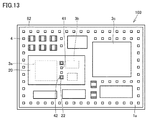
- FIG. 13 shows a state in which the first sealing resin 6a of the module 103 is removed, as viewed from directly below.
- Two first columnar conductors 41 and two second columnar conductors 42 are arranged inside the laminated body 20.
- the number and positional relationship shown here are just examples, and are not always the same.
- the first columnar conductor 41 penetrates the first opening 21 of the laminated body 20, and the first columnar conductor 41 is in contact with the surrounding laminated body 20.
- the second columnar conductor 42 penetrates the second opening 22 of the laminated body 20, and the second columnar conductor 42 is separated from the surrounding laminated body 20.
- the second opening 22 is larger than the outer shape of the second columnar conductor 42.
- the end surface of the first columnar conductor 41 opposite to the substrate 1 is used to ground the first columnar conductor 41, and further, the end surface of the second columnar conductor 42 opposite to the substrate 1 is used.
- the end face can be used to make a signal connection to the second columnar conductor 42. Since the second columnar conductor 42 can be arranged in the region of the laminated body 20 when viewed in a plan view, the degree of freedom in design is increased.
- the substrate 1 has a second surface 1b as a surface opposite to the first surface 1a, and other components are mounted on the second surface 1b. That is, it is preferable that the module has a so-called double-sided mounting structure. This is because by adopting this configuration, it is possible to mount more parts using the substrate 1 having a limited area, and it is possible to efficiently realize high functionality.
- the present embodiment an example is shown in which the lower surface of the substrate 1 is the first surface 1a and the resin film 20 is arranged on the first surface 1a side, but the present invention is not limited to this, and for example, in the second embodiment. In the configuration of the module 102 shown, other components may be mounted on the second surface 1b.
- the upper surface of the substrate 1 is the first surface 1a
- the resin film 20 is arranged on the first surface 1a side
- other components are mounted on the second surface 1b as the lower surface of the substrate 1.
- It may be the configuration that has been set.
- the second surface 1b is covered with a sealing resin different from the sealing resin 6 that covers the first surface 1a.
- the second shield film 82 preferably extends so as to cover the side surface of the sealing resin on the second surface 1b side.
- Substrate 1a 1st surface, 1b 2nd surface, 2 Insulation layer, 3,3a, 3b, 3c parts, 4 Columnar conductor, 6 Encapsulation resin, 6a 1st encapsulation resin, 6b 2nd encapsulation resin, 7 Resin film, 11 ground electrode, 12 signal electrode, 14 pad electrode, 15 conductor pattern, 16 conductor via, 17 external electrode, 20 laminate, 21 1st opening, 22 2nd opening, 41 1st columnar conductor, 42 2nd columnar conductor, 81 1st shield film, 82 2nd shield film, 101, 102, 103 modules.
Landscapes
- Engineering & Computer Science (AREA)
- Microelectronics & Electronic Packaging (AREA)
- Physics & Mathematics (AREA)
- Electromagnetism (AREA)
- Shielding Devices Or Components To Electric Or Magnetic Fields (AREA)
- Structures Or Materials For Encapsulating Or Coating Semiconductor Devices Or Solid State Devices (AREA)
Abstract
モジュールは、第1面(1a)を有する基板(1)と、第1面(1a)に実装された1以上の部品としての部品(3a,3b)と、前記1以上の部品を、前記1以上の部品の形状に沿って覆い、かつ、第1面(1a)の一部も覆う樹脂膜(7)と、樹脂膜(7)に重なるように形成された第1シールド膜(81)と、第1面(1a)、前記1以上の部品および第1シールド膜(81)を覆うように配置された封止樹脂としての第1封止樹脂(6a)とを備える。樹脂膜(7)および第1シールド膜(81)を含む積層体(20)は第1開口部(21)を有する。第1封止樹脂(6a)および第1開口部(21)を貫通して第1面(1a)に電気的に接続されるように第1柱状導体(41)が配置されている。第1シールド膜(81)は第1開口部(21)において第1柱状導体(41)に電気的に接続されている。
Description
本発明は、モジュールに関するものである。
特許第6459019号(特許文献1)には、第1熱硬化性樹脂組成物を含む第1領域を有し、絶縁性を有する第1層と、第2熱硬化性樹脂組成物を含む第2層と、これら2つの層の間に配置された導電性材料とを備える封止用積層シートが、記載されている。特許文献1には、この封止用積層シートを用いた電子部品モジュールも記載されている。この電子部品モジュールにおいては、回路基板に複数の電子部品が搭載されており、これらの複数の電子部品が封止用積層シートによって一括して封止されている。
封止用積層シートに含まれる導電性材料を以てシールド性能を確保しようとする場合、この導電性材料を接地することが求められる。特許文献1では、第1層にグランド接続のための孔を設けることによって導電性材料を露出させることが記載されている。しかし、この構成では、グランド接続を確実に行なうことが困難であった。また、封止用積層シートに含まれる導電性材料のグランド接続(以下、「接地」ともいう。)の自由度は低い。
そこで、本発明は、シールド性能を強化し、なおかつ、接地を容易に行なえるモジュールを提供することを目的とする。
上記目的を達成するため、本発明に基づくモジュールは、第1面を有する基板と、上記第1面に実装された1以上の部品と、上記1以上の部品を、上記1以上の部品の形状に沿って覆い、かつ、上記第1面の一部も覆う樹脂膜と、上記樹脂膜に重なるように形成された第1シールド膜と、上記第1面、上記1以上の部品および上記第1シールド膜を覆うように配置された封止樹脂とを備え、上記樹脂膜および上記第1シールド膜を含む積層体は第1開口部を有し、上記封止樹脂および上記第1開口部を貫通して上記第1面に電気的に接続されるように第1柱状導体が配置されており、上記第1シールド膜は上記第1開口部において上記第1柱状導体に電気的に接続されている。
本発明によれば、シールド性能を強化することができる。さらに、第1柱状導体が第1開口部を貫通するようにして第1シールド膜と第1柱状導体とが電気的に接続されているので、接地を容易に行なうことができる。
図面において示す寸法比は、必ずしも忠実に現実のとおりを表しているとは限らず、説明の便宜のために寸法比を誇張して示している場合がある。以下の説明において、上または下の概念に言及する際には、絶対的な上または下を意味するとは限らず、図示された姿勢の中での相対的な上または下を意味する場合がある。
(実施の形態1)
図1~図8を参照して、本発明に基づく実施の形態1におけるモジュールについて説明する。
図1~図8を参照して、本発明に基づく実施の形態1におけるモジュールについて説明する。
本実施の形態におけるモジュール101の外観を図1に示す。モジュール101の全体は、通常、直方体形状を有している。図1では、モジュール101の実装面とは反対側の面が主に見えている。モジュール101の実装面が見える向きで見たときの斜視図を図2に示す。モジュール101の断面図を図3に示す。
モジュール101は、基板1を備える。基板1は、複数の絶縁層2を積層して形成されたものである。基板1は、第1面1aおよび第2面1bを有する。ここで示す例では、第1面1aにも、第2面1bにもそれぞれ複数の部品が実装されている。基板1の第1面1aおよび第2面1bには、それぞれパッド電極14が配置されている。第1面1aには、少なくとも部品3a,3b,3cがパッド電極14を介して実装されている。部品3a,3bおよび第1面1aに密着するように、積層体20が配置されている。積層体20は、樹脂膜7と第1シールド膜81とを含む。積層体20は、シート状のものを変形させたものである。第1面1aは、第1封止樹脂6aによって封止されている。第2面1bにもいくつかの部品3が実装されている。第2面1bおよび第2面1bに実装された部品3は、第2封止樹脂6bによって封止されている。モジュール101の上面および側面は、第2シールド膜82によって覆われている。
モジュール101の構成については、以下のように表現することができる。本実施の形態におけるモジュール101は、第1面1aを有する基板1と、第1面1aに実装された1以上の部品としての部品3a,3bと、樹脂膜7と、樹脂膜7に重なるように形成された第1シールド膜81と、封止樹脂としての第1封止樹脂6aとを備える。樹脂膜7は、前記1以上の部品としての部品3a,3bを、これらの部品3a,3bの形状に沿って覆い、かつ、第1面1aの一部も覆う。封止樹脂としての第1封止樹脂6aは、第1面1a、部品3a,3bおよび第1シールド膜81を覆うように配置されている。ここでは、部品3a,3bが樹脂膜7によって覆われていることに注目して説明しているが、樹脂膜7は部品3a,3b以外の部品も覆っていてよい。本実施の形態で示す例では、樹脂膜7は、部品3a,3b以外の部品も同時に覆っている。
積層体20は、樹脂膜7および第1シールド膜81の2層のみを含むものであってもよく、これら2層に加えて他の層を含んでいてもよい。樹脂膜7および第1シールド膜81を含む積層体20は、第1開口部21を有する。第1封止樹脂6aおよび第1開口部21を貫通して第1面1aに電気的に接続されるように第1柱状導体41が配置されている。第1シールド膜81は第1開口部21において第1柱状導体41に電気的に接続されている。
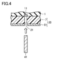
第1開口部21における第1シールド膜81と第1柱状導体41との間の電気的接続の構造については、以下のことがいえる。この部分においては、たとえば図4に示すように、先に基板1の第1面1aに、第1開口部21を有する積層体20が付着している状態で、矢印に示すように第1柱状導体41を挿入することによって、図5に示すような構造としてもよい。
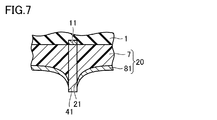
逆に、図6に示すように、先に基板1の第1面1aに、第1柱状導体41が実装されている状態で、矢印に示すように積層体20を組み合わせることによって、積層体20に予め設けられている第1開口部21に第1柱状導体41が挿入されるようにしてもよい。この場合、図7に示す構造が得られる。モジュール101においては、積層体20の第1開口部21の近傍は、図5、図7のいずれの構造であってもよい。図5および図7に示したのは、あくまで例示であって、この通りの形状に限定されるものではない。図5および図7では、第1開口部21が挿入されたことによって積層体20が変形しているが、このような変形が必ず生じるとは限らない。
基板1の第1面1aには、接地電極11が配置されている。第1柱状導体41の基板1側の端は、接地電極11に接続されている。
モジュール101の第1封止樹脂6aを取り去った状態を、真下から見たところを、図8に示す。外周に沿って柱状導体4が配列されている。第1面1aの一部の領域を覆うように積層体20が配置されている。積層体20によって一部の部品が隠されており、これらの部品は破線で表示されている。積層体20を貫通する2本の第1柱状導体41が、部品3aと部品3bとの間に、配置されている。ここで示した柱状導体4および第1柱状導体41の個数および配置は、あくまで一例として示すものであって、この通りに限定するものではない。図8に示すように、第1面1aには、部品3a,3b,3cの他にもいくつかの部品が実装されていてもよい。部品3a.3bに加えてさらに他の部品が、積層体20に覆われていてもよい。
本実施の形態では、部品3aに近い位置において部品3aを覆うように第1シールド膜81が配置されるので、シールド性能を強化することができる。第1シールド膜81は、部品3aの高さとほぼ変わらない高さで配置することができるので、モジュールの低背化を図ることができる。さらに、積層体20が第1開口部21を有し、第1柱状導体41が第1開口部21を貫通するようにして第1シールド膜81と第1柱状導体41とが電気的に接続されているので、接地を容易に、確実に行なうことができる。
なお、本実施の形態で示したように、第1柱状導体41の基板1とは反対側の端は、最外面に露出していることが好ましい。この構成を採用することにより、第1柱状導体41の基板1とは反対側の端面を利用して、第1柱状導体41に対する接地を行なうことができる。モジュール101が、第1封止樹脂6aの基板1とは反対側の面を利用してマザー基板などに実装される構成である場合には、第1柱状導体41の基板1とは反対側の端面を、マザー基板などに予め用意された接地電極などと直接接続することができる。
なお、本実施の形態で示したように、前記1以上の部品は、複数の部品であり、第1柱状導体41は、前記複数の部品の間に配置されていることが好ましい。この構成を採用することにより、部品同士の間のシールドを強化することができるからである。本実施の形態では、第1柱状導体41が、部品3aと部品3bとの間に配置されているので、部品3a,3b間のシールドを強化することができる。
なお、ここでは、「1以上の部品」として、部品3a,3bに注目して説明したが、部品の数は3個以上であってもよい。また、「1以上の部品」は、当然、1個だけの部品であってもよい。たとえば積層体20が覆う部品の数は、1個であってもよい。
(実施の形態2)
図9~図10を参照して、本発明に基づく実施の形態2におけるモジュールについて説明する。本実施の形態におけるモジュール102の断面図を図9に示す。本実施の形態では、基板1の第1面1aおよび第2面1bの位置関係が、実施の形態1に比べて逆である。すなわち、基板1の上面が第1面1aとなっており、下面が第2面1bとなっている。第1面1aに部品3a,3b,3c,3dが実装されている。このうち部品3a,3bを覆うように、積層体20が配置されている。積層体20は第1開口部21を有する。モジュール102は、第1面1a、部品3aおよび第1シールド膜81を覆うように配置された封止樹脂6を備える。封止樹脂6および第1開口部21を貫通して第1面1aに電気的に接続されるように第1柱状導体41が配置されている。モジュール102は、封止樹脂6を覆う第2シールド膜82を備え、第1柱状導体41は、第2シールド膜82に電気的に接続されている。図9におけるX-X線に関する矢視断面図を、図10に示す。ただし、図10では、説明の便宜のため、封止樹脂6を取り去った状態を示している。
図9~図10を参照して、本発明に基づく実施の形態2におけるモジュールについて説明する。本実施の形態におけるモジュール102の断面図を図9に示す。本実施の形態では、基板1の第1面1aおよび第2面1bの位置関係が、実施の形態1に比べて逆である。すなわち、基板1の上面が第1面1aとなっており、下面が第2面1bとなっている。第1面1aに部品3a,3b,3c,3dが実装されている。このうち部品3a,3bを覆うように、積層体20が配置されている。積層体20は第1開口部21を有する。モジュール102は、第1面1a、部品3aおよび第1シールド膜81を覆うように配置された封止樹脂6を備える。封止樹脂6および第1開口部21を貫通して第1面1aに電気的に接続されるように第1柱状導体41が配置されている。モジュール102は、封止樹脂6を覆う第2シールド膜82を備え、第1柱状導体41は、第2シールド膜82に電気的に接続されている。図9におけるX-X線に関する矢視断面図を、図10に示す。ただし、図10では、説明の便宜のため、封止樹脂6を取り去った状態を示している。
本実施の形態では、封止樹脂6を第2シールド膜82が覆っており、この第2シールド膜82に対して第1柱状導体41が電気的に接続されているので、第1シールド膜81と第2シールド膜82とのいずれか一方を接地することによって、他方も接地することができる。たとえば基板1に内蔵されるグランド導体パターンを基板1の側面に露出させて第2シールド膜82と電気的に接続させることによって、第2シールド膜82を接地する構成である場合には、第1シールド膜81は第1柱状導体41を経由して第2シールド膜82と電気的に接続されているので、第1シールド膜81に別ルートでの独自の接地をしなくても、第2シールド膜82のグランド電位を利用して接地することができる。
なお、図9に示した例では、第1面1aのみに部品が実装されており、第2面1bに部品が実装されていないが、これはあくまで一例に過ぎない。たとえば第1面1aの他に第2面1bにも部品が実装されていてもよい。下面である第2面1bに部品が実装され、この第2面1bおよび実装された部品が封止樹脂で覆われた構成であってもよい。
(実施の形態3)
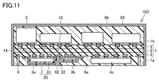
図11~図13を参照して、本発明に基づく実施の形態3におけるモジュールについて説明する。本実施の形態におけるモジュール103の断面図を図11に示す。本実施の形態では、基板1の第1面1aおよび第2面1bの位置関係が、実施の形態1と同じであり、実施の形態2に比べて逆である。すなわち、基板1の下面が第1面1aとなっており、上面が第2面1bとなっている。モジュール103では、第1面1aに第2柱状導体42が実装されている。第2柱状導体42およびその近傍を拡大したところを図12に示す。
図11~図13を参照して、本発明に基づく実施の形態3におけるモジュールについて説明する。本実施の形態におけるモジュール103の断面図を図11に示す。本実施の形態では、基板1の第1面1aおよび第2面1bの位置関係が、実施の形態1と同じであり、実施の形態2に比べて逆である。すなわち、基板1の下面が第1面1aとなっており、上面が第2面1bとなっている。モジュール103では、第1面1aに第2柱状導体42が実装されている。第2柱状導体42およびその近傍を拡大したところを図12に示す。
モジュール103では、第1面1aには信号電極12が設けられている。樹脂膜7および第1シールド膜81を含む積層体20は、第2開口部22を有する。封止樹脂としての第1封止樹脂6aおよび第2開口部22を貫通して信号電極12に電気的に接続されるように第2柱状導体42が配置されている。第1シールド膜81は第2開口部22において信号電極12から離隔している。すなわち、第2開口部22の径は、第2柱状導体42の径よりも大きい。第2柱状導体42の基板1とは反対側の端は、最外面に露出している。
モジュール103の第1封止樹脂6aを取り去った状態を、真下から見たところを、図13に示す。積層体20の内部に、2本の第1柱状導体41と2本の第2柱状導体42とが配置されている。ここで示した本数と位置関係はあくまで一例であって、この通りとは限らない。第1柱状導体41は、積層体20の第1開口部21を貫通しており、第1柱状導体41は周囲の積層体20と接している。第2柱状導体42は、積層体20の第2開口部22を貫通しており、第2柱状導体42は周囲の積層体20から離隔している。第2開口部22は、第2柱状導体42の外形より大きくなっている。
本実施の形態では、第1柱状導体41の基板1とは反対側の端面を利用して、第1柱状導体41に対する接地を行ない、さらに、第2柱状導体42の基板1とは反対側の端面を利用して、第2柱状導体42に対する信号接続を行なうことができる。第2柱状導体42は、平面図で見たときに積層体20の領域の中にも配置することができるので、設計の自由度が高くなる。
本実施の形態で示したように、基板1は、第1面1aとは反対側の面として第2面1bを有し、第2面1bに他の部品が実装されていることが好ましい。すなわち、モジュールがいわゆる両面実装構造を備えることが好ましい。この構成を採用することにより、限られた面積の基板1を用いてより多くの部品を実装することができ、効率良く、高機能を実現することができるからである。本実施の形態では、基板1の下面が第1面1aであって、第1面1a側に樹脂膜20が配置されている例を示したが、これに限らず、たとえば実施の形態2で示したモジュール102の構成において、第2面1bに他の部品が実装されていてもよい。すなわち、基板1の上面が第1面1aであって、第1面1a側に樹脂膜20が配置されていて、これとは別に基板1の下面としての第2面1bに他の部品が実装されている構成であってもよい。この場合、第2面1bは、第1面1aを覆う封止樹脂6とは別の封止樹脂によって覆われていることが好ましい。第2シールド膜82は、第2面1b側の封止樹脂の側面を覆うように延在していることが好ましい。
なお、上記実施の形態のうち複数を適宜組み合わせて採用してもよい。
なお、今回開示した上記実施の形態はすべての点で例示であって制限的なものではない。本発明の範囲は請求の範囲によって示され、請求の範囲と均等の意味および範囲内でのすべての変更を含むものである。
なお、今回開示した上記実施の形態はすべての点で例示であって制限的なものではない。本発明の範囲は請求の範囲によって示され、請求の範囲と均等の意味および範囲内でのすべての変更を含むものである。
1 基板、1a 第1面、1b 第2面、2 絶縁層、3,3a,3b,3c 部品、4 柱状導体、6 封止樹脂、6a 第1封止樹脂、6b 第2封止樹脂、7 樹脂膜、11 接地電極、12 信号電極、14 パッド電極、15 導体パターン、16 導体ビア、17 外部電極、20 積層体、21 第1開口部、22 第2開口部、41 第1柱状導体、42 第2柱状導体、81 第1シールド膜、82 第2シールド膜、101,102,103 モジュール。
Claims (7)
- 第1面を有する基板と、
前記第1面に実装された1以上の部品と、
前記1以上の部品を、前記1以上の部品の形状に沿って覆い、かつ、前記第1面の一部も覆う樹脂膜と、
前記樹脂膜に重なるように形成された第1シールド膜と、
前記第1面、前記1以上の部品および前記第1シールド膜を覆うように配置された封止樹脂とを備え、
前記樹脂膜および前記第1シールド膜を含む積層体は第1開口部を有し、
前記封止樹脂および前記第1開口部を貫通して前記第1面に電気的に接続されるように第1柱状導体が配置されており、
前記第1シールド膜は前記第1開口部において前記第1柱状導体に電気的に接続されている、モジュール。 - 前記第1柱状導体の前記基板とは反対側の端は、最外面に露出している、請求項1に記載のモジュール。
- 前記1以上の部品は、複数の部品であり、前記第1柱状導体は、前記複数の部品の間に配置されている、請求項1または2に記載のモジュール。
- 前記第1面には信号電極が設けられており、
前記樹脂膜および前記第1シールド膜を含む積層体は第2開口部を有し、
前記封止樹脂および前記第2開口部を貫通して前記信号電極に電気的に接続されるように第2柱状導体が配置されており、
前記第2開口部の径は、前記第2柱状導体の径よりも大きい、請求項1から3のいずれか1項に記載のモジュール。 - 前記第2柱状導体の前記基板とは反対側の端は、最外面に露出している、請求項4に記載のモジュール。
- 前記封止樹脂を覆う第2シールド膜を備え、
前記第1柱状導体は、前記第2シールド膜に電気的に接続されている、請求項1に記載のモジュール。 - 前記基板は、前記第1面とは反対側の面として第2面を有し、
前記第2面に他の部品が実装されている、請求項1から6のいずれか1項に記載のモジュール。
Priority Applications (2)
| Application Number | Priority Date | Filing Date | Title |
|---|---|---|---|
| CN202190000545.6U CN219395428U (zh) | 2020-06-16 | 2021-06-04 | 模块 |
| US18/063,794 US12446157B2 (en) | 2020-06-16 | 2022-12-09 | Module |
Applications Claiming Priority (2)
| Application Number | Priority Date | Filing Date | Title |
|---|---|---|---|
| JP2020103942 | 2020-06-16 | ||
| JP2020-103942 | 2020-06-16 |
Related Child Applications (1)
| Application Number | Title | Priority Date | Filing Date |
|---|---|---|---|
| US18/063,794 Continuation US12446157B2 (en) | 2020-06-16 | 2022-12-09 | Module |
Publications (1)
| Publication Number | Publication Date |
|---|---|
| WO2021256299A1 true WO2021256299A1 (ja) | 2021-12-23 |
Family
ID=79267871
Family Applications (1)
| Application Number | Title | Priority Date | Filing Date |
|---|---|---|---|
| PCT/JP2021/021338 Ceased WO2021256299A1 (ja) | 2020-06-16 | 2021-06-04 | モジュール |
Country Status (3)
| Country | Link |
|---|---|
| US (1) | US12446157B2 (ja) |
| CN (1) | CN219395428U (ja) |
| WO (1) | WO2021256299A1 (ja) |
Families Citing this family (1)
| Publication number | Priority date | Publication date | Assignee | Title |
|---|---|---|---|---|
| WO2021131774A1 (ja) * | 2019-12-27 | 2021-07-01 | 株式会社村田製作所 | モジュール |
Citations (5)
| Publication number | Priority date | Publication date | Assignee | Title |
|---|---|---|---|---|
| US20120020039A1 (en) * | 2008-12-19 | 2012-01-26 | Stmicroelectronics (Grenoble) Sas | Surface-mounted shielded multicomponent assembly |
| US20130082367A1 (en) * | 2011-09-30 | 2013-04-04 | Samsung Electro-Mechanics Co., Ltd. | Semiconductor package and method of manufacturing the same |
| WO2018101384A1 (ja) * | 2016-12-02 | 2018-06-07 | 株式会社村田製作所 | 高周波モジュール |
| WO2019098316A1 (ja) * | 2017-11-20 | 2019-05-23 | 株式会社村田製作所 | 高周波モジュール |
| WO2020067468A1 (ja) * | 2018-09-28 | 2020-04-02 | 株式会社村田製作所 | 電子部品モジュールおよび電子部品モジュールの製造方法 |
Family Cites Families (7)
| Publication number | Priority date | Publication date | Assignee | Title |
|---|---|---|---|---|
| US5140110A (en) * | 1986-03-13 | 1992-08-18 | Nintendo Co. Ltd. | Printed circuit board capable of preventing electromagnetic interference |
| JP4096605B2 (ja) * | 2002-04-23 | 2008-06-04 | 日本電気株式会社 | 半導体装置および半導体装置のシールド形成方法 |
| US8959757B2 (en) * | 2011-12-29 | 2015-02-24 | Rf Micro Devices, Inc. | Method of manufacturing an electronic module |
| JP6459019B2 (ja) | 2014-05-22 | 2019-01-30 | ナガセケムテックス株式会社 | 封止用積層シートおよびその製造方法ならびに封止用積層シートを用いて封止された実装構造体およびその製造方法 |
| JP6900660B2 (ja) | 2016-11-28 | 2021-07-07 | 株式会社村田製作所 | シールド層を有するモジュール |
| WO2018164158A1 (ja) | 2017-03-08 | 2018-09-13 | 株式会社村田製作所 | 高周波モジュール |
| WO2018181708A1 (ja) | 2017-03-31 | 2018-10-04 | 株式会社村田製作所 | モジュール |
-
2021
- 2021-06-04 CN CN202190000545.6U patent/CN219395428U/zh active Active
- 2021-06-04 WO PCT/JP2021/021338 patent/WO2021256299A1/ja not_active Ceased
-
2022
- 2022-12-09 US US18/063,794 patent/US12446157B2/en active Active
Patent Citations (5)
| Publication number | Priority date | Publication date | Assignee | Title |
|---|---|---|---|---|
| US20120020039A1 (en) * | 2008-12-19 | 2012-01-26 | Stmicroelectronics (Grenoble) Sas | Surface-mounted shielded multicomponent assembly |
| US20130082367A1 (en) * | 2011-09-30 | 2013-04-04 | Samsung Electro-Mechanics Co., Ltd. | Semiconductor package and method of manufacturing the same |
| WO2018101384A1 (ja) * | 2016-12-02 | 2018-06-07 | 株式会社村田製作所 | 高周波モジュール |
| WO2019098316A1 (ja) * | 2017-11-20 | 2019-05-23 | 株式会社村田製作所 | 高周波モジュール |
| WO2020067468A1 (ja) * | 2018-09-28 | 2020-04-02 | 株式会社村田製作所 | 電子部品モジュールおよび電子部品モジュールの製造方法 |
Also Published As
| Publication number | Publication date |
|---|---|
| US12446157B2 (en) | 2025-10-14 |
| US20230105635A1 (en) | 2023-04-06 |
| CN219395428U (zh) | 2023-07-21 |
Similar Documents
| Publication | Publication Date | Title |
|---|---|---|
| US7478474B2 (en) | Method of manufacturing shielded electronic circuit units | |
| TWI453768B (zh) | Composite flexible circuit cable | |
| WO2019098316A1 (ja) | 高周波モジュール | |
| CN107710406A (zh) | 高频模块 | |
| US12424528B2 (en) | Module | |
| JPWO2012144326A1 (ja) | コネクタおよびコネクタの製造方法 | |
| WO2021131776A1 (ja) | モジュール | |
| WO2021176871A1 (ja) | モジュール | |
| JP7060171B2 (ja) | 伝送線路及び回路基板 | |
| KR20120049607A (ko) | 표시장치 | |
| US12446157B2 (en) | Module | |
| US12144159B2 (en) | Module | |
| CN220173699U (zh) | 电路模块 | |
| US12193162B2 (en) | Module | |
| JP2008172015A (ja) | 電磁シールドテープおよび電磁シールドテープを用いた電子機器 | |
| JP2008078205A (ja) | 基板組立体及びその製造方法、電子部品組立体及びその製造方法、電子装置 | |
| US20220310317A1 (en) | Electronic component module | |
| JP7131624B2 (ja) | モジュール | |
| JP2004056155A (ja) | モジュール部品 | |
| JP2007123722A (ja) | シールド構造 | |
| WO2021140850A1 (ja) | モジュール | |
| US20240324158A1 (en) | Module | |
| US12193148B2 (en) | Module | |
| CN113015314B (zh) | 电路板装置 | |
| JP5347880B2 (ja) | 電磁シールド、電子機器 |
Legal Events
| Date | Code | Title | Description |
|---|---|---|---|
| 121 | Ep: the epo has been informed by wipo that ep was designated in this application |
Ref document number: 21825766 Country of ref document: EP Kind code of ref document: A1 |
|
| WWE | Wipo information: entry into national phase |
Ref document number: 202190000545.6 Country of ref document: CN |
|
| NENP | Non-entry into the national phase |
Ref country code: DE |
|
| 122 | Ep: pct application non-entry in european phase |
Ref document number: 21825766 Country of ref document: EP Kind code of ref document: A1 |
|
| NENP | Non-entry into the national phase |
Ref country code: JP |