WO2021256083A1 - 冷却装置および半導体モジュール - Google Patents
冷却装置および半導体モジュール Download PDFInfo
- Publication number
- WO2021256083A1 WO2021256083A1 PCT/JP2021/016327 JP2021016327W WO2021256083A1 WO 2021256083 A1 WO2021256083 A1 WO 2021256083A1 JP 2021016327 W JP2021016327 W JP 2021016327W WO 2021256083 A1 WO2021256083 A1 WO 2021256083A1
- Authority
- WO
- WIPO (PCT)
- Prior art keywords
- bottom plate
- top plate
- cooling device
- tip
- side wall
- Prior art date
- Legal status (The legal status is an assumption and is not a legal conclusion. Google has not performed a legal analysis and makes no representation as to the accuracy of the status listed.)
- Ceased
Links
Images




Classifications
-
- H—ELECTRICITY
- H10—SEMICONDUCTOR DEVICES; ELECTRIC SOLID-STATE DEVICES NOT OTHERWISE PROVIDED FOR
- H10W—GENERIC PACKAGES, INTERCONNECTIONS, CONNECTORS OR OTHER CONSTRUCTIONAL DETAILS OF DEVICES COVERED BY CLASS H10
- H10W40/00—Arrangements for thermal protection or thermal control
- H10W40/40—Arrangements for thermal protection or thermal control involving heat exchange by flowing fluids
- H10W40/47—Arrangements for thermal protection or thermal control involving heat exchange by flowing fluids by flowing liquids, e.g. forced water cooling
-
- H—ELECTRICITY
- H10—SEMICONDUCTOR DEVICES; ELECTRIC SOLID-STATE DEVICES NOT OTHERWISE PROVIDED FOR
- H10W—GENERIC PACKAGES, INTERCONNECTIONS, CONNECTORS OR OTHER CONSTRUCTIONAL DETAILS OF DEVICES COVERED BY CLASS H10
- H10W40/00—Arrangements for thermal protection or thermal control
- H10W40/20—Arrangements for cooling
- H10W40/22—Arrangements for cooling characterised by their shape, e.g. having conical or cylindrical projections
- H10W40/226—Arrangements for cooling characterised by their shape, e.g. having conical or cylindrical projections characterised by projecting parts, e.g. fins to increase surface area
-
- H—ELECTRICITY
- H05—ELECTRIC TECHNIQUES NOT OTHERWISE PROVIDED FOR
- H05K—PRINTED CIRCUITS; CASINGS OR CONSTRUCTIONAL DETAILS OF ELECTRIC APPARATUS; MANUFACTURE OF ASSEMBLAGES OF ELECTRICAL COMPONENTS
- H05K7/00—Constructional details common to different types of electric apparatus
- H05K7/20—Modifications to facilitate cooling, ventilating, or heating
-
- H—ELECTRICITY
- H10—SEMICONDUCTOR DEVICES; ELECTRIC SOLID-STATE DEVICES NOT OTHERWISE PROVIDED FOR
- H10W—GENERIC PACKAGES, INTERCONNECTIONS, CONNECTORS OR OTHER CONSTRUCTIONAL DETAILS OF DEVICES COVERED BY CLASS H10
- H10W40/00—Arrangements for thermal protection or thermal control
- H10W40/01—Manufacture or treatment
- H10W40/03—Manufacture or treatment of arrangements for cooling
- H10W40/037—Assembling together parts thereof
-
- H—ELECTRICITY
- H10—SEMICONDUCTOR DEVICES; ELECTRIC SOLID-STATE DEVICES NOT OTHERWISE PROVIDED FOR
- H10W—GENERIC PACKAGES, INTERCONNECTIONS, CONNECTORS OR OTHER CONSTRUCTIONAL DETAILS OF DEVICES COVERED BY CLASS H10
- H10W76/00—Containers; Fillings or auxiliary members therefor; Seals
- H10W76/60—Seals
-
- H—ELECTRICITY
- H10—SEMICONDUCTOR DEVICES; ELECTRIC SOLID-STATE DEVICES NOT OTHERWISE PROVIDED FOR
- H10W—GENERIC PACKAGES, INTERCONNECTIONS, CONNECTORS OR OTHER CONSTRUCTIONAL DETAILS OF DEVICES COVERED BY CLASS H10
- H10W40/00—Arrangements for thermal protection or thermal control
- H10W40/20—Arrangements for cooling
- H10W40/25—Arrangements for cooling characterised by their materials
- H10W40/255—Arrangements for cooling characterised by their materials having a laminate or multilayered structure, e.g. direct bond copper [DBC] ceramic substrates
-
- H—ELECTRICITY
- H10—SEMICONDUCTOR DEVICES; ELECTRIC SOLID-STATE DEVICES NOT OTHERWISE PROVIDED FOR
- H10W—GENERIC PACKAGES, INTERCONNECTIONS, CONNECTORS OR OTHER CONSTRUCTIONAL DETAILS OF DEVICES COVERED BY CLASS H10
- H10W76/00—Containers; Fillings or auxiliary members therefor; Seals
- H10W76/40—Fillings or auxiliary members in containers, e.g. centering rings
- H10W76/42—Fillings
- H10W76/47—Solid or gel fillings
-
- H—ELECTRICITY
- H10—SEMICONDUCTOR DEVICES; ELECTRIC SOLID-STATE DEVICES NOT OTHERWISE PROVIDED FOR
- H10W—GENERIC PACKAGES, INTERCONNECTIONS, CONNECTORS OR OTHER CONSTRUCTIONAL DETAILS OF DEVICES COVERED BY CLASS H10
- H10W90/00—Package configurations
Definitions
- the present invention relates to a cooling device and a semiconductor module.
- Patent Document 1 Japanese Patent Application Laid-Open No. 2014-179563
- the sealing performance it is preferable to improve the sealing performance to prevent the leakage of the refrigerant of the cooling device.
- a cooling device for a semiconductor module may include a semiconductor chip.
- the cooling device may include a top plate.
- the top plate may have a lower surface.
- the cooling device may include a bottom plate.
- the bottom plate may be arranged so as to have a space that functions as a refrigerant flow portion between the bottom plate and the lower surface of the top plate.
- the cooling device may include side walls.
- the side wall may connect the top plate and the bottom plate.
- the side wall may surround the refrigerant flow section.
- the side wall may have a fixing portion.
- the fixing portion may be provided on at least one of the top plate and the bottom plate. The fixing portion may be fixed to the top plate or the bottom plate by a fixing material.
- the fixing portion may have a tip portion.
- the tip portion may be arranged so as to face the top plate or the bottom plate.
- the fixed portion may have a separating portion.
- the separating portion may be adjacent to the tip portion in the first direction in which the refrigerant flowing portion and the side wall are lined up.
- the separating portion may be arranged more away from the top plate or the bottom plate arranged facing the tip portion than the tip portion.
- the second aspect of the present invention provides a semiconductor module.
- the semiconductor module may include a cooling device according to the first aspect of the present invention.
- the semiconductor module may include a semiconductor device.
- the semiconductor device may be arranged above the top plate.
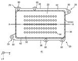
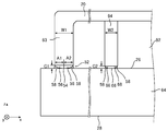
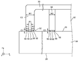
- FIG. 1 It is a schematic sectional drawing which shows an example of the semiconductor module 100 which concerns on one Embodiment of this invention. It is a figure which shows an example of the shape of the ceiling part 41 in the bottom view (xy plane). It is a figure which shows an example of the fixing part 52 and the cooling fin 94 near the fixing part 52 in a cooling device 10. It is a figure which shows the other example of the fixing part 52 and the cooling fin 94 near the fixing part 52 in a cooling device 10. It is a figure which shows the other example of the fixing part 52 and the cooling fin 94 near the fixing part 52 in a cooling device 10. It is a figure which shows the other example of the fixing part 52 and the cooling fin 94 near the fixing part 52 in a cooling device 10.
- FIG. 7 It is a schematic sectional drawing which shows an example of the semiconductor module 200 which concerns on other embodiment of this invention. It is a figure which shows an example of the fixing part 52 in the cooling device 10 of FIG. 7, and the cooling fin 94 near the fixing part 52. It is a main circuit diagram of the semiconductor module 100 which concerns on one Embodiment of this invention.
- FIG. 1 is a schematic cross-sectional view showing an example of a semiconductor module 100 according to an embodiment of the present invention.
- the semiconductor module 100 includes a semiconductor device 70 and a cooling device 10.
- the semiconductor device 70 of this example is mounted on the cooling device 10.
- the plane of the cooling device 10 on which the semiconductor device 70 is mounted is defined as the xy plane, and the plane perpendicular to the xy plane is defined as the z-axis.
- the direction from the cooling device 10 to the semiconductor device 70 in the z-axis direction is referred to as an up direction, and the opposite direction is referred to as a down direction, but the up and down directions are not limited to the gravity direction.
- the upper surface is referred to as an upper surface and the lower surface is referred to as a lower surface.
- the semiconductor device 70 includes one or more semiconductor chips 78 such as power semiconductor chips.
- the semiconductor chip 78 is provided with an insulated gate bipolar transistor (IGBT) formed on a semiconductor substrate such as silicon.
- IGBT insulated gate bipolar transistor
- the semiconductor device 70 has a circuit board 76 and an accommodating portion 72.
- the circuit board 76 is provided with a circuit pattern on one surface of an insulating substrate and a heat dissipation plate on the other surface.
- a semiconductor chip 78 is fixed to the circuit board 76 via solder or the like.
- the accommodating portion 72 is formed of an insulating material such as resin.
- the accommodating portion 72 of this example is a resin case made of resin.
- the accommodating portion 72 has an internal space for accommodating the semiconductor chip 78, the circuit board 76, wiring, and the like.
- the internal space of the accommodating portion 72 may be filled with a sealing member 74 that seals the semiconductor chip 78, the circuit board 76, the wiring, and the like.
- the sealing member 74 is an insulating member such as a silicone gel or an epoxy resin.
- the cooling device 10 is a cooling device for the semiconductor module 100.
- the cooling device 10 cools the semiconductor device 70.
- the cooling device 10 has a ceiling portion 41 and a bottom portion 40.
- the ceiling portion 41 has a top plate 20, a side wall 63, and cooling fins 94.
- the top plate 20 and the side wall 63 may be configured as an integral member by plastically deforming one metal plate.
- the bottom portion 40 has a bottom plate 64.
- the ceiling 41 may have a top plate 20, and the bottom 40 may have a bottom plate 64, side walls 63 and cooling fins 94.
- the bottom plate 64 and the side wall 63 may be configured as an integral member.
- the cooling fin 94 may be fixed to at least one of the bottom plate 64 and the top plate 20 with a wax material or the like.
- the cooling fin 94 may be configured as a member integrated with the bottom plate 64 and the top plate 20 by casting or the like.
- the top plate 20 may be a plate-shaped metal plate having an upper surface 22 and a lower surface 24 parallel to the xy plane.
- the top plate 20 is made of a metal containing aluminum.
- the semiconductor device 70 is placed on the upper surface 22 of the top plate 20.
- the heat generated by the semiconductor chip 78 is transferred to the top plate 20.
- a heat conductive member such as a circuit board 76, a metal plate, and solder is arranged between the top plate 20 and the semiconductor chip 78.
- the circuit board 76 may be directly fixed to the upper surface 22 of the top plate 20 by solder or the like.
- the accommodating portion 72 is provided on the upper surface 22 of the top plate 20 so as to surround the area where the circuit board 76 and the like are arranged.
- the circuit board 76 does not have a heat dissipation plate, and the insulating layer on the side opposite to the semiconductor chip 78 of the circuit board 76 may be directly fixed to the upper surface 22 of the top plate 20.
- the side wall 63 connects the top plate 20 and the bottom plate 64. That is, the ceiling portion 41 of this example is connected to the bottom portion 40 at the side wall 63.
- the side wall 63 may be firmly fixed to at least one of the top plate 20 and the bottom plate 64 by a brazing material.
- the side wall 63 is fixed to the bottom plate 64 by a wax material.
- the side wall 63 may be fixed to the top plate 20 by a brazing material.
- the side wall 63 may be fixed to both the bottom plate 64 and the top plate 20 with a wax material or the like.
- the side wall 63 surrounds the refrigerant flow section 92 on the xy surface.
- the side wall 63 defines the refrigerant flow section 92 on the xy plane.
- the refrigerant flow unit 92 is arranged on the lower surface 24 side of the top plate 20.
- the refrigerant distribution unit 92 is a region in which a refrigerant such as water flows.
- the refrigerant flow unit 92 may be a closed space in contact with the lower surface 24 of the top plate 20.
- the bottom plate 64 is closely fixed to the side wall 63 surrounding the refrigerant flow portion 92 on the xy surface by a wax material. As a result, the refrigerant flow unit 92 is sealed.
- the bottom plate 64 may be closely fixed to the upper surface 26 of the bottom plate 64 with a sealing material, an adhesive, or other members.
- the "adhesion” refers to a state in which the refrigerant inside the refrigerant flow unit 92 does not leak from the intimate portion.
- Cooling fins 94 are arranged inside the refrigerant flow unit 92.
- the cooling fin 94 may be fixed to at least one of the top plate 20 and the bottom plate 64 with a wax material.
- the cooling fin 94 is fixed to the bottom plate 64 by a brazing material.
- the cooling fins 94 may be separated from or in contact with the unbrazed top plate 20 or the bottom plate 64.
- the cooling fin 94 may be integrally formed with one of the top plate 20 or the bottom plate 64 and may be brazed to the other of the top plate 20 or the bottom plate 64. Further, by passing the refrigerant in the vicinity of the cooling fins 94, the heat generated by the semiconductor chip 78 is transferred to the refrigerant. As a result, the semiconductor device 70 can be cooled.
- the bottom portion 40 has a bottom plate 64.
- the bottom plate 64 is arranged so as to have a space that functions as a refrigerant flow unit 92 with the lower surface 24 of the top plate 20.
- the bottom plate 64 of this example is provided with two or more openings 42 for introducing or deriving the refrigerant into the refrigerant flow section 92.
- a pipe 90 for transporting the refrigerant is connected to the opening 42.
- the pipe 90 projects from the cooling fin 94 to the lower surface 28 side (z-axis negative side in this example) of the cooling fin 94 with the bottom plate 64 as a reference.
- the side wall 63 and the bottom plate 64 are brazed.
- the top plate 20, the side wall 63, and the bottom plate 64 are made of a metal having the same composition, and the brazing material is made of a metal having a melting point lower than that of the top plate 20 and the like.
- a metal containing aluminum may be used as the metal.
- an aluminum alloy such as an Al—Mn based alloy (3000 series aluminum alloy) or an Al—Mg—Si based alloy (6000 series aluminum alloy) may be used.
- an aluminum alloy such as an Al—Si based alloy (4000 series aluminum alloy) may be used.
- the aluminum alloy used in this example preferably has a proof stress in the range of 35 to 65 MPa at room temperature. Yield strength is a stress that causes a permanent strain of 0.2% when unloaded.
- the side wall 63 has a fixing portion 52.
- the side wall 63 has a fixing portion 52 at the tip thereof.
- the tip of the side wall 63 is the portion of the side wall 63 closest to the bottom plate 64 or the top plate 20. In the example of FIG. 1, the end portion of the side wall 63 in the z-axis direction is used as the tip.
- the side wall 63 has a fixing portion 52 with respect to at least one of the top plate 20 and the bottom plate 64.
- the fixing portion 52 may be fixed to the top plate 20 or the bottom plate 64 with a wax material. In the example of FIG. 1, the fixing portion 52 is in close contact with the bottom plate 64 by a wax material.
- the fixed portion 52 has a tip portion and a separated portion.
- the tip portion in this example is the portion of the side wall 63 closest to the bottom plate 64.
- the tip portion may be a plane parallel to the bottom plate 64, or may be an apex arranged facing the bottom plate 64.
- the separated portion is a portion adjacent to the tip portion and the distance from the bottom plate 64 is larger than the distance between the tip portion and the bottom plate 64.
- the separating portion is provided at a position facing the bottom plate 64 in the z-axis direction. That is, a relatively large space is provided between the separation portion and the bottom plate 64.
- the fixing portion 52 has a tapered shape.
- the brazing material between the tip portion and the bottom plate 64 flows into the space between the separating portion and the bottom plate 64.
- the wax material flowing out from between the tip portion and the bottom plate 64 can also contribute to the close contact fixing between the side wall 63 and the bottom plate 64.
- a thick layer of wax material can be formed in the z-axis direction between the separation portion and the bottom plate 64. Therefore, the sealing performance of the cooling device 10 can be improved.
- FIG. 2 is a diagram showing an example of the shape of the ceiling portion 41 in the bottom view (xy surface).
- viewing from the lower surface side of the top plate 20 or the like is referred to as bottom view, and viewing from the upper surface side is referred to as top view.
- the bottom view and top view drawings are views in which the positions of each member are projected onto the xy plane.
- the ceiling portion 41 of FIG. 1 corresponds to the AA cross section of FIG.
- the width of the side wall 63 is shown to be large.
- the sizes of the members do not always match.
- the ceiling portion 41 of this example has a top plate 20, a fixing portion 52 (side wall 63), cooling fins 94, and an outer edge portion 62 in a bottom view.
- the ceiling portion 41 has two sets of opposite sides 36, 38 in a top view.
- the ceiling portion 41 of this example has a substantially rectangular shape having a short side 36 and a long side 38.
- the ceiling portion 41 has four corner portions 29.
- the direction in which the short side 36 extends is the y-axis
- the direction in which the long side 38 extends is the x-axis.
- the side wall 63 in this example is substantially perpendicular to the xy plane.
- the outer edge portion 62 is provided on the outer edge of the ceiling portion 41.
- the outer edge portion 62 of this example is a region of the top plate 20 outside the side wall 63.
- the outer edge portion 62 is provided outside the refrigerant flow portion 92 surrounded by the side wall 63.
- the outer edge portion 62 may be provided so as to surround at least a part of the periphery of the side wall 63. In the example of FIG. 2, the outer edge portion 62 surrounds the side wall 63 in the y-axis direction. Further, the outer edge portion 62 may be provided so as to surround the entire circumference of the side wall 63.
- the outer edge portion 62 has a fastening portion 80.
- the fastening portion 80 fastens the ceiling portion 41 and the bottom portion 40.
- the bottom portion 40 may also have a fastening portion.
- the fastening portion 80 may be used to fix the semiconductor module 100 to an external device.
- the fastening portion 80 is a region in which the top plate 20 and the bottom plate 64 are directly or indirectly in close contact with each other and overlapped in the z-axis direction, and a through hole penetrating the top plate 20 and the bottom portion 40 is formed. Area.
- the top plate 20 is provided with a plurality of fastening portions 80. At least one fastening portion 80 may be provided at the corner portion 29. In this example, fastening portions 80 are provided at all the corner portions 29. Further, the fastening portion 80 may or may not be provided on each long side 38. The fastening portion 80 may or may not be provided on each of the short sides 36.
- the cooling fin 94 is arranged inside the refrigerant flow unit 92 surrounded by the side wall 63.
- a plurality of cooling fins 94 may be evenly arranged in the x-axis direction.
- a plurality of cooling fins 94 may be evenly arranged in the y-axis direction.
- the cooling fins 94 may be unevenly arranged in each direction.
- FIG. 3 is a diagram showing an example of a fixing portion 52 and a cooling fin 94 in the vicinity of the fixing portion 52 in the cooling device 10.
- FIG. 3 shows the fixing portion 52 and the cooling fin 94 closest to the fixing portion 52.
- a part of the top plate 20 and the bottom plate 64 is also shown.
- the fixed portion 52 has a tip portion 54.
- the tip portion 54 may be arranged so as to face the top plate 20 or the bottom plate 64. In the example of FIG. 3, the tip portion 54 is arranged so as to face the bottom plate 64. The tip portion 54 may be arranged in direct contact with the bottom plate 64.
- the fixed portion 52 has a separating portion 56.
- the separating portion 56 is adjacent to the tip portion 54 in the first direction (x-axis direction in FIG. 3) in which the refrigerant flow portion 92 and the side wall 63 are lined up. In the yz cross section, since the refrigerant flow section 92 and the side wall 63 are lined up in the y-axis direction, the y-axis direction is the first direction.
- the separating portion 56 may be arranged more away from the top plate 20 or the bottom plate 64 arranged so as to face the tip portion 54 than the tip portion 54. In this example, the distance between the separating portion 56 and the bottom plate 64 is larger than the distance between the tip portion 54 and the bottom plate 64.
- the separating portion 56 may have an inclined surface having an inclination with respect to the z-axis. That is, the distance of the separating portion 56 from the tip portion 54 in the first direction may increase as the distance from the bottom plate 64 increases.
- the inclination of the inclination of the separating portion 56 may be constant or may change.
- the wax material 58 is arranged between the fixing portion 52 and the bottom plate 64.
- the wax material 58 may be arranged between the separating portion 56 and the bottom plate 64.
- the wax material 58 may also be arranged between the tip 54 and the bottom plate 64.
- the fixing portion 52 is brazed to the bottom plate 64 with a brazing material 58. Since the fixing portion 52 has the tip portion 54 and the separating portion 56, the sealing performance of the cooling device 10 can be improved as described above.
- the ceiling portion 41 and the bottom portion 40, particularly the separation portion 56, may be forged products. By forming these by forging, a tapered shape can be easily formed. For example, the corner of the metal plate can be plastically deformed by hitting it with a tool to form the separated portion 56 of the fixed portion 52.
- the fixed portion 52 may have a plurality of separated portions 56.
- the fixing portion 52 has two separating portions 56.
- the tip portion 54 may be sandwiched between a plurality of separating portions 56 in the first direction (x-axis direction in FIG. 3). That is, the surface of the fixing portion 52 facing the bottom plate 64 may have a convex shape.
- the thick film wax material 58 can be formed on both sides of the tip portion 54, so that the sealing performance can be improved.
- the fixing portion 52 may have a plurality of tip portions 54, and the separating portion 56 may be sandwiched between the plurality of tip portions 54. That is, the surface of the fixing portion 52 facing the bottom plate 64 may have a concave shape. Even with such a shape, the sealing performance of the cooling device 10 can be improved.
- the tip of the cooling fin 94 may have a tapered shape. That is, the tip of the cooling fin 94 may have a tip portion 66 and a separation portion 68.
- the tip portion 66 may have the same structure as the tip portion 54
- the separation portion 68 may have the same structure as the separation portion 56.
- the separating portion 68 may be arranged so as to surround the tip portion 54 in the top view.
- the tip portion 66 is arranged so as to face the bottom plate 64.
- the separating portion 68 is arranged farther from the bottom plate 64 than the tip portion 66.
- the width W1 of the side wall 63 may be smaller than the width W2 of the cooling fin 94. If the width W2 of the cooling fin 94 is not uniformly determined depending on the measurement direction, the measured value in the smallest direction may be the width W2.
- the tip of the cooling fin 94 does not have to have a tapered shape.
- the wax material 58 may be arranged between the tip of the cooling fin 94 and the bottom plate 64. That is, the wax material 58 may be arranged between the tip portion 66 and the bottom plate 64 or between the separation portion 68 and the bottom plate 64.
- the tip of the cooling fin 94 is brazed to the bottom plate 64 by the brazing material 58.
- the maximum separation distance C2 between the tip of the cooling fin 94 and the upper surface 26 of the bottom plate 64 may be smaller than the maximum separation distance C1 between the separation portion 56 and the upper surface 26 of the bottom plate 64.
- the maximum distance C2 between the tip of the cooling fin 94 and the upper surface 26 of the bottom plate 64 may be the distance between the end of the cooling fin 94 in the first direction and the upper surface 26 of the bottom plate 64.
- the maximum separation distance C1 between the separation portion 56 and the upper surface 26 of the bottom plate 64 may be the distance between the end portion of the separation portion 56 in the first direction and the upper surface 26 of the bottom plate 64.
- the sealing performance of the cooling device 10 is improved.
- the cooling fins 94 can also be secured in terms of bondability or load bearing capacity.
- the width B1 of the tip portion 54 in the first direction may be smaller than the sum of the widths of the plurality of separation portions 56 in the first direction.
- the width B1 of the tip portion 54 may be smaller than the sum of the width A1 and the width A2 of the two separating portions 56 sandwiching the tip portion 54 in the first direction.
- the width B1 of the tip portion 54 in the first direction may be smaller than the width of each of the plurality of separation portions 56 in the first direction. That is, the width B1 of the tip portion 54 may be smaller than any of the width A1 and the width A2 of the two separating portions 56 that sandwich the tip portion 54 in the first direction. With such a configuration, the ratio of the separated portion 56 to the tip portion 54 in the fixed portion 52 can be further increased. By providing the width B1 of the tip portion 54, the load bearing capacity of the side wall 63 can be ensured.
- the widths A1 and A2 of the separation portion 56 in the first direction may be 0.5 mm or more, preferably 0.65 mm or more, respectively.
- the widths A1 and A2 of the separation portion 56 in the first direction may be 1.0 mm or less, preferably 0.85 mm or less, respectively.
- the width B1 of the tip portion 54 in the first direction may be 1.0 mm or less, preferably 0.5 mm or less.
- the width W1 of the side wall 63 in the first direction is the sum of the widths A1 and A2 of the separation portion 56 in the first direction and the width B1 of the tip portion 54 in the first direction (X-axis direction).
- the width W1 of the side wall 63 is, for example, 2.0 mm.
- the width B1 of the tip portion 54 in the first direction may be 1/4 or less of the width W1 of the side wall in the first direction.
- the width B1 of the tip portion 54 in the first direction By setting the width B1 of the tip portion 54 in the first direction to 1/4 or less of the width W1 of the side wall in the first direction, the ratio of the separated portion 56 to the tip portion 54 in the fixed portion 52 can be increased.
- the width B1 of the tip portion 54 may be 1/10 or more of the width W1 of the side wall 63.
- the maximum separation distance C1 may be smaller than the width of each of the plurality of separation portions 56 in the first direction. That is, the maximum separation distance C1 may be smaller than any of the width A1 and the width A2 of the two separation portions 56 that sandwich the tip portion 54 in the first direction. Further, the maximum separation distance C1 may be 0.1 mm or more, preferably 0.2 mm or more. Further, the maximum separation distance C1 may be 1.0 mm or less, preferably 0.5 mm or less. With such a configuration, it is possible to prevent the separation portion 56 and the upper surface 26 of the bottom plate 64 from being too far apart from each other and deteriorating the bondability.
- the maximum separation distance C2 may be 0.0 mm or more.
- the case where the maximum separation distance C2 is 0.0 mm is a case where the tip of the cooling fin 94 does not have a tapered shape.
- the maximum separation distance C2 may be 0.2 mm or less.
- the maximum separation distance C2 is, for example, 0.1 mm.
- FIG. 4 is a diagram showing another example of the fixing portion 52 and the cooling fin 94 in the vicinity of the fixing portion 52 in the cooling device 10.
- the cooling device 10 of FIG. 4 is different from the cooling device 10 of FIG. 3 in that the fixing portion 52 has an arc shape in a predetermined cross section.
- the fixing portion 52 of this example has a convex arc shape on the bottom plate 64 side in the xz cross section.
- the configuration other than the shape of the fixing portion 52 may be the same as that of the cooling device 10 of FIG.
- the width B1 of the tip portion 54 in the first direction (x-axis direction in this example) may be a value as close to 0 as possible.
- the width B1 may be 10% or less of the width A1 or the width A2, and may be 5% or less.
- the inclination of the separated portion 56 near the tip portion 54 changes more gently than the tapered shape. Therefore, as compared with the tapered shape, the distance portion 56 near the tip portion 54 is closer to the bottom plate 64, and the adhesion between the distance portion 56 of the side wall 63 and the bottom plate 64 can be further strengthened. As described above, in the cooling fin 94, a space in which the wax material flows can be further secured between the separating portion 68 and the bottom plate 64.
- FIG. 5 is a diagram showing another example of the fixing portion 52 and the cooling fin 94 in the vicinity of the fixing portion 52 in the cooling device 10.
- the cooling device 10 of FIG. 5 differs from the cooling device 10 of FIG. 3 in that the tip of the cooling fin 94 has an arc shape in a predetermined cross section.
- the cooling fin 94 may have a convex arc shape on the bottom plate 64 side in any cross section perpendicular to the xy plane.
- the configuration other than the cooling fins 94 may be the same as that of the cooling device 10 of FIG.
- the tip of the cooling fin 94 has an arc shape, the inclination of the separation portion 68 near the tip portion 66 changes more gently than the tapered shape. Therefore, as compared with the tapered shape, the distance portion 68 near the tip portion 66 is closer to the bottom plate 64, and the adhesion between the distance portion 68 and the bottom plate 64 can be further strengthened. As described above, in the fixing portion 52 of the side wall 63, a space in which the wax material flows can be further secured between the separating portion 56 and the bottom plate 64.
- FIG. 6 is a diagram showing another example of the fixing portion 52 and the cooling fin 94 in the vicinity of the fixing portion 52 in the cooling device 10.
- the cooling device 10 of FIG. 6 is different from the cooling device 10 of FIG. 4 in that the tip of the cooling fin 94 has an arc shape.
- the configuration other than the cooling fins 94 may be the same as that of the cooling device 10 of FIG.
- FIG. 7 is a schematic cross-sectional view showing an example of the semiconductor module 200 according to another embodiment of the present invention.
- the semiconductor module 100 of FIG. 7 is different from the semiconductor module 100 of FIG. 1 in the configuration of the ceiling portion 41 and the bottom portion 40.
- the configuration other than the ceiling portion 41 and the bottom portion 40 may be the same as that of the semiconductor module 100.
- the ceiling portion 41 has a top plate 20. Further, the bottom portion 40 has a bottom plate 64, a side wall 63, and a cooling fin 94.
- the components of the ceiling portion 41 and the bottom portion 40 may be integrally formed. That is, the bottom plate 64, the side wall 63, and the cooling fins 94 may be integrally formed.
- the side wall 63 has a fixing portion 52.
- the side wall 63 may have a fixing portion 52 at its tip.
- the fixing portion 52 is in close contact with the top plate 20 by a wax material.
- the fixed portion 52 has a tip portion and a separated portion. Since at least a part of the separating portion and the top plate 20 are arranged apart from each other, the wax material flowing in the separating portion adheres the side wall 63 and the top plate 20 without vacuoles. Therefore, even when the configurations of the ceiling portion 41 and the bottom portion 40 are different, the sealing performance of the cooling device 10 can be improved.
- FIG. 8 is a diagram showing an example of a fixing portion 52 and a cooling fin 94 in the vicinity of the fixing portion 52 in the cooling device 10 of FIG. 7.
- FIG. 8 shows a reference numeral common to that of FIG.
- the widths A1 and A2 of the separation portion 56, the width B1 of the tip portion 54, the width W1 of the side wall 63, and the width W2 of the cooling fin 94 may be the same as those in FIG.
- the wax material 58 is arranged between the fixing portion 52 and the top plate 20. That is, the wax material 58 may be arranged between the tip portion 54 and the top plate 20 or between the separation portion 56 and the top plate 20.
- the wax material 58 adheres the fixing portion 52 and the top plate 20.
- the fixing portion 52 is brazed to the top plate 20. Since the fixing portion 52 has the tip portion 54 and the separating portion 56, the brazing material 58 can bond the separating portion 56 and the top plate 20 without vacuoles. Therefore, the sealing performance of the cooling device 10 can be improved.
- the wax material 58 is arranged between the tip of the cooling fin 94 and the top plate 20. That is, the wax material 58 may be arranged between the tip portion 66 and the top plate 20 or between the separation portion 68 and the top plate 20.
- the brazing material 58 adheres the tip of the cooling fin 94 to the top plate 20. In other words, the tip of the cooling fin 94 is brazed to the top plate 20.
- the maximum separation distance C4 between the tip of the cooling fin 94 and the lower surface 24 of the top plate 20 may be smaller than the maximum separation distance C3 between the separation portion 56 and the lower surface 24 of the top plate 20.
- the maximum separation distance C4 between the tip of the cooling fin 94 and the lower surface 24 of the top plate 20 may be the height of the tip 66.
- the maximum separation distance C3 between the separation portion 56 and the lower surface 24 of the top plate 20 may be the height of the tip portion 54.
- the sealing performance of the cooling device 10 is improved by making the maximum separation distance C4 between the tip of the cooling fin 94 and the lower surface 24 of the top plate 20 smaller than the maximum separation distance C3 between the separation portion 56 and the lower surface 24 of the top plate 20. At the same time, it is possible to secure the bondability or the load bearing capacity of the cooling fin 94 as well.
- the maximum separation distance C3 may be smaller than the width of each of the plurality of separation portions 56 in the first direction. That is, the maximum separation distance C3 may be smaller than any of the width A1 and the width A2 of the two separation portions 56 that sandwich the tip portion 54 in the first direction. Further, the maximum separation distance C3 may be 0.1 mm or more, preferably 0.2 mm or more. Further, the maximum separation distance C3 may be 1.0 mm or less, preferably 0.5 mm or less. The maximum separation distance C3 is, for example, 0.3 mm. With such a configuration, it is possible to prevent the separation portion 56 and the lower surface 24 of the top plate 20 from being too far apart from each other and deteriorating the bondability.
- the maximum separation distance C4 may be 0.0 mm or more.
- the case where the maximum separation distance C4 is 0.0 mm is a case where the tip of the cooling fin 94 does not have a tapered shape.
- the maximum separation distance C4 may be 0.2 mm or less.
- the maximum separation distance C4 is, for example, 0.1 mm.
- FIG. 9 is a main circuit diagram of the semiconductor module 100 according to one embodiment of the present invention.
- the semiconductor module 100 may be a part of an in-vehicle unit that drives a vehicle motor.
- the semiconductor module 100 may function as a three-phase AC inverter circuit having output terminals U, V and W.
- the semiconductor chips 78-1, 78-2 and 78-3 may form the lower arm in the semiconductor module 100, and the plurality of semiconductor chips 78-4, 78-5 and 78-6 may form the upper arm in the semiconductor module 100.
- a set of semiconductor chips 78-1 and 78-4 may form a leg.
- a set of semiconductor chips 78-2, 78-5 and a set of semiconductor chips 78-3, 78-6 may also form a leg.
- the emitter electrode may be electrically connected to the input terminal N1 and the collector electrode may be electrically connected to the output terminal U.
- the emitter electrode may be electrically connected to the output terminal U and the collector electrode may be electrically connected to the input terminal P1.
- the emitter electrode may be electrically connected to the input terminals N2 and N3, respectively, and the collector electrode may be electrically connected to the output terminals V and W, respectively.
- the emitter electrode may be electrically connected to the output terminals V and W, respectively, and the collector electrode may be electrically connected to the input terminals P2 and P3, respectively.
- Each semiconductor chip 78-1 to 78-6 may be alternately switched by a signal input to the control electrode pad of the semiconductor chip 78.
- each semiconductor chip 78 may generate heat during switching.
- the input terminals P1, P2 and P3 may be connected to the positive electrode of the external power supply, the input terminals N1, N2 and N3 may be connected to the negative electrode, and the output terminals U, V and W may be connected to the load.
- the input terminals P1, P2 and P3 may be electrically connected to each other, and the other input terminals N1, N2 and N3 may also be electrically connected to each other.
- the plurality of semiconductor chips 78-1 to 78-6 may be RC-IGBT (reverse conducting IGBT) semiconductor chips, respectively.
- the IGBT and the freewheeling diode (FWD) may be integrally formed, and the IGBT and the FWD may be connected in antiparallel.
- the plurality of semiconductor chips 78-1 to 78-6 may each include a combination of a transistor and a diode such as a MOSFET or an IGBT.
- the chip substrate of the transistor and the diode may be a silicon substrate, a silicon carbide substrate, or a gallium nitride substrate.
Landscapes
- Physics & Mathematics (AREA)
- Thermal Sciences (AREA)
- Engineering & Computer Science (AREA)
- Microelectronics & Electronic Packaging (AREA)
- Cooling Or The Like Of Semiconductors Or Solid State Devices (AREA)
- Cooling Or The Like Of Electrical Apparatus (AREA)
Priority Applications (3)
| Application Number | Priority Date | Filing Date | Title |
|---|---|---|---|
| CN202180006651.XA CN114747003A (zh) | 2020-06-17 | 2021-04-22 | 冷却装置和半导体模块 |
| JP2022532347A JP7424489B2 (ja) | 2020-06-17 | 2021-04-22 | 冷却装置および半導体モジュール |
| US17/747,994 US12424507B2 (en) | 2020-06-17 | 2022-05-18 | Cooling apparatus and semiconductor module |
Applications Claiming Priority (2)
| Application Number | Priority Date | Filing Date | Title |
|---|---|---|---|
| JP2020-104802 | 2020-06-17 | ||
| JP2020104802 | 2020-06-17 |
Related Child Applications (1)
| Application Number | Title | Priority Date | Filing Date |
|---|---|---|---|
| US17/747,994 Continuation US12424507B2 (en) | 2020-06-17 | 2022-05-18 | Cooling apparatus and semiconductor module |
Publications (1)
| Publication Number | Publication Date |
|---|---|
| WO2021256083A1 true WO2021256083A1 (ja) | 2021-12-23 |
Family
ID=79267744
Family Applications (1)
| Application Number | Title | Priority Date | Filing Date |
|---|---|---|---|
| PCT/JP2021/016327 Ceased WO2021256083A1 (ja) | 2020-06-17 | 2021-04-22 | 冷却装置および半導体モジュール |
Country Status (4)
| Country | Link |
|---|---|
| US (1) | US12424507B2 (https=) |
| JP (1) | JP7424489B2 (https=) |
| CN (1) | CN114747003A (https=) |
| WO (1) | WO2021256083A1 (https=) |
Cited By (2)
| Publication number | Priority date | Publication date | Assignee | Title |
|---|---|---|---|---|
| DE102022209698A1 (de) | 2022-09-15 | 2024-03-21 | Robert Bosch Gesellschaft mit beschränkter Haftung | Fluiddurchströmbarer Kühler zum Kühlen eines Leistungsmoduls |
| JP2025022793A (ja) * | 2023-08-01 | 2025-02-14 | アイエムエイチ インコーポレイテッド | 放熱装置一体型半導体用放熱基板の製造方法 |
Families Citing this family (1)
| Publication number | Priority date | Publication date | Assignee | Title |
|---|---|---|---|---|
| JP7577948B2 (ja) * | 2020-09-15 | 2024-11-06 | 富士電機株式会社 | 冷却器及び半導体装置 |
Citations (3)
| Publication number | Priority date | Publication date | Assignee | Title |
|---|---|---|---|---|
| JP2013024483A (ja) * | 2011-07-21 | 2013-02-04 | Mitsubishi Electric Corp | プレート積層型冷却器 |
| JP2016120526A (ja) * | 2011-03-03 | 2016-07-07 | 昭和電工株式会社 | 鍛造加工方法 |
| JP2019160852A (ja) * | 2018-03-08 | 2019-09-19 | 昭和電工株式会社 | ヒートシンクの製造方法 |
Family Cites Families (18)
| Publication number | Priority date | Publication date | Assignee | Title |
|---|---|---|---|---|
| JPH1158001A (ja) * | 1997-08-07 | 1999-03-02 | Hitachi Zosen Corp | 両面開先溶接方法 |
| JP2006114571A (ja) | 2004-10-12 | 2006-04-27 | Hitachi Ltd | 半導体装置およびこれを実装した電子機器 |
| JP4799098B2 (ja) * | 2005-09-20 | 2011-10-19 | 株式会社東芝 | ジェットポンプ |
| JP4797077B2 (ja) * | 2009-02-18 | 2011-10-19 | 株式会社日立製作所 | 半導体パワーモジュール、電力変換装置、および、半導体パワーモジュールの製造方法 |
| JP5542627B2 (ja) | 2010-11-11 | 2014-07-09 | 新電元工業株式会社 | 接続板、接合構造及び半導体装置 |
| JP2014011447A (ja) * | 2012-06-29 | 2014-01-20 | Nakamura Mfg Co Ltd | 発熱体冷却装置 |
| JP6186146B2 (ja) | 2013-03-15 | 2017-08-23 | 株式会社Uacj | 熱交換器 |
| US9633967B2 (en) | 2013-10-21 | 2017-04-25 | Nsk Ltd. | Semiconductor module |
| WO2016203884A1 (ja) * | 2015-06-17 | 2016-12-22 | 富士電機株式会社 | パワー半導体モジュール、流路部材及びパワー半導体モジュール構造体 |
| JP6870253B2 (ja) * | 2016-09-20 | 2021-05-12 | 富士電機株式会社 | 半導体装置及び半導体装置の製造方法 |
| CA3036731A1 (en) * | 2016-10-14 | 2018-04-19 | Dana Canada Corporation | Heat exchanger having bypass seal with retention clip |
| FR3080174B1 (fr) * | 2018-01-29 | 2020-05-29 | Valeo Systemes Thermiques | Plaque pour echangeur de chaleur |
| JP7067129B2 (ja) * | 2018-03-06 | 2022-05-16 | 富士電機株式会社 | 冷却装置、半導体モジュールおよび車両 |
| JP7116576B2 (ja) * | 2018-04-02 | 2022-08-10 | 富士電機株式会社 | 冷却装置、半導体モジュールおよび車両 |
| JP7205071B2 (ja) * | 2018-04-02 | 2023-01-17 | 富士電機株式会社 | 冷却装置、半導体モジュールおよび車両 |
| JP7159617B2 (ja) * | 2018-05-25 | 2022-10-25 | 富士電機株式会社 | 冷却装置、半導体モジュール、車両および製造方法 |
| WO2020003757A1 (ja) * | 2018-06-27 | 2020-01-02 | 富士電機株式会社 | 冷却装置、半導体モジュールおよび車両 |
| JP7367394B2 (ja) * | 2018-11-22 | 2023-10-24 | 富士電機株式会社 | 半導体モジュール、車両および製造方法 |
-
2021
- 2021-04-22 JP JP2022532347A patent/JP7424489B2/ja active Active
- 2021-04-22 WO PCT/JP2021/016327 patent/WO2021256083A1/ja not_active Ceased
- 2021-04-22 CN CN202180006651.XA patent/CN114747003A/zh active Pending
-
2022
- 2022-05-18 US US17/747,994 patent/US12424507B2/en active Active
Patent Citations (3)
| Publication number | Priority date | Publication date | Assignee | Title |
|---|---|---|---|---|
| JP2016120526A (ja) * | 2011-03-03 | 2016-07-07 | 昭和電工株式会社 | 鍛造加工方法 |
| JP2013024483A (ja) * | 2011-07-21 | 2013-02-04 | Mitsubishi Electric Corp | プレート積層型冷却器 |
| JP2019160852A (ja) * | 2018-03-08 | 2019-09-19 | 昭和電工株式会社 | ヒートシンクの製造方法 |
Cited By (3)
| Publication number | Priority date | Publication date | Assignee | Title |
|---|---|---|---|---|
| DE102022209698A1 (de) | 2022-09-15 | 2024-03-21 | Robert Bosch Gesellschaft mit beschränkter Haftung | Fluiddurchströmbarer Kühler zum Kühlen eines Leistungsmoduls |
| JP2025022793A (ja) * | 2023-08-01 | 2025-02-14 | アイエムエイチ インコーポレイテッド | 放熱装置一体型半導体用放熱基板の製造方法 |
| JP7818849B2 (ja) | 2023-08-01 | 2026-02-24 | アイエムエイチ インコーポレイテッド | 放熱装置一体型半導体用放熱基板の製造方法 |
Also Published As
| Publication number | Publication date |
|---|---|
| CN114747003A (zh) | 2022-07-12 |
| US12424507B2 (en) | 2025-09-23 |
| US20220278014A1 (en) | 2022-09-01 |
| JPWO2021256083A1 (https=) | 2021-12-23 |
| JP7424489B2 (ja) | 2024-01-30 |
Similar Documents
| Publication | Publication Date | Title |
|---|---|---|
| JP7067129B2 (ja) | 冷却装置、半導体モジュールおよび車両 | |
| US11538736B2 (en) | Cooling apparatus, semiconductor module, and vehicle | |
| US12424507B2 (en) | Cooling apparatus and semiconductor module | |
| CN111146160B (zh) | 半导体模块和车辆 | |
| JP7116576B2 (ja) | 冷却装置、半導体モジュールおよび車両 | |
| JP7147859B2 (ja) | 半導体装置、半導体モジュールおよび車両 | |
| JP2020072106A (ja) | 半導体装置 | |
| US11355420B2 (en) | Cooling apparatus, semiconductor module, and vehicle | |
| JP2020136366A (ja) | 半導体モジュール、車両および製造方法 | |
| US11908772B2 (en) | Semiconductor module and vehicle | |
| JP6575739B1 (ja) | 半導体装置、半導体装置の製造方法および電力変換装置 | |
| US20210313249A1 (en) | Semiconductor module and vehicle | |
| US12127382B2 (en) | Semiconductor module with cooling fins in a matrix form | |
| US20220165712A1 (en) | Power module | |
| US11582889B2 (en) | Semiconductor module and vehicle | |
| CN116344469A (zh) | 功率半导体模块 | |
| US20230420323A1 (en) | Semiconductor module, and manufacturing method for semiconductor module |
Legal Events
| Date | Code | Title | Description |
|---|---|---|---|
| 121 | Ep: the epo has been informed by wipo that ep was designated in this application |
Ref document number: 21825662 Country of ref document: EP Kind code of ref document: A1 |
|
| ENP | Entry into the national phase |
Ref document number: 2022532347 Country of ref document: JP Kind code of ref document: A |
|
| NENP | Non-entry into the national phase |
Ref country code: DE |
|
| 122 | Ep: pct application non-entry in european phase |
Ref document number: 21825662 Country of ref document: EP Kind code of ref document: A1 |