WO2021246302A1 - スイッチング電源装置、スイッチ制御装置、車載機器、及び車両 - Google Patents
スイッチング電源装置、スイッチ制御装置、車載機器、及び車両 Download PDFInfo
- Publication number
- WO2021246302A1 WO2021246302A1 PCT/JP2021/020345 JP2021020345W WO2021246302A1 WO 2021246302 A1 WO2021246302 A1 WO 2021246302A1 JP 2021020345 W JP2021020345 W JP 2021020345W WO 2021246302 A1 WO2021246302 A1 WO 2021246302A1
- Authority
- WO
- WIPO (PCT)
- Prior art keywords
- switch
- state
- power supply
- switching power
- connectable
- Prior art date
- Legal status (The legal status is an assumption and is not a legal conclusion. Google has not performed a legal analysis and makes no representation as to the accuracy of the status listed.)
- Ceased
Links
Images


Classifications
-
- H—ELECTRICITY
- H02—GENERATION; CONVERSION OR DISTRIBUTION OF ELECTRIC POWER
- H02M—APPARATUS FOR CONVERSION BETWEEN AC AND AC, BETWEEN AC AND DC, OR BETWEEN DC AND DC, AND FOR USE WITH MAINS OR SIMILAR POWER SUPPLY SYSTEMS; CONVERSION OF DC OR AC INPUT POWER INTO SURGE OUTPUT POWER; CONTROL OR REGULATION THEREOF
- H02M3/00—Conversion of DC power input into DC power output
- H02M3/02—Conversion of DC power input into DC power output without intermediate conversion into AC
- H02M3/04—Conversion of DC power input into DC power output without intermediate conversion into AC by static converters
- H02M3/10—Conversion of DC power input into DC power output without intermediate conversion into AC by static converters using discharge tubes with control electrode or semiconductor devices with control electrode
- H02M3/145—Conversion of DC power input into DC power output without intermediate conversion into AC by static converters using discharge tubes with control electrode or semiconductor devices with control electrode using devices of a triode or transistor type requiring continuous application of a control signal
- H02M3/155—Conversion of DC power input into DC power output without intermediate conversion into AC by static converters using discharge tubes with control electrode or semiconductor devices with control electrode using devices of a triode or transistor type requiring continuous application of a control signal using semiconductor devices only
- H02M3/156—Conversion of DC power input into DC power output without intermediate conversion into AC by static converters using discharge tubes with control electrode or semiconductor devices with control electrode using devices of a triode or transistor type requiring continuous application of a control signal using semiconductor devices only with automatic control of output voltage or current, e.g. switching regulators
- H02M3/158—Conversion of DC power input into DC power output without intermediate conversion into AC by static converters using discharge tubes with control electrode or semiconductor devices with control electrode using devices of a triode or transistor type requiring continuous application of a control signal using semiconductor devices only with automatic control of output voltage or current, e.g. switching regulators including plural semiconductor devices as final control devices for a single load
-
- H—ELECTRICITY
- H02—GENERATION; CONVERSION OR DISTRIBUTION OF ELECTRIC POWER
- H02M—APPARATUS FOR CONVERSION BETWEEN AC AND AC, BETWEEN AC AND DC, OR BETWEEN DC AND DC, AND FOR USE WITH MAINS OR SIMILAR POWER SUPPLY SYSTEMS; CONVERSION OF DC OR AC INPUT POWER INTO SURGE OUTPUT POWER; CONTROL OR REGULATION THEREOF
- H02M1/00—Details of apparatus for conversion
- H02M1/0003—Details of control, feedback or regulation circuits
- H02M1/0009—Devices or circuits for detecting current in a converter
-
- H—ELECTRICITY
- H02—GENERATION; CONVERSION OR DISTRIBUTION OF ELECTRIC POWER
- H02M—APPARATUS FOR CONVERSION BETWEEN AC AND AC, BETWEEN AC AND DC, OR BETWEEN DC AND DC, AND FOR USE WITH MAINS OR SIMILAR POWER SUPPLY SYSTEMS; CONVERSION OF DC OR AC INPUT POWER INTO SURGE OUTPUT POWER; CONTROL OR REGULATION THEREOF
- H02M1/00—Details of apparatus for conversion
- H02M1/0003—Details of control, feedback or regulation circuits
- H02M1/0016—Control circuits providing compensation of output voltage deviations using feedforward of disturbance parameters
- H02M1/0022—Control circuits providing compensation of output voltage deviations using feedforward of disturbance parameters the disturbance parameters being input voltage fluctuations
-
- H—ELECTRICITY
- H02—GENERATION; CONVERSION OR DISTRIBUTION OF ELECTRIC POWER
- H02M—APPARATUS FOR CONVERSION BETWEEN AC AND AC, BETWEEN AC AND DC, OR BETWEEN DC AND DC, AND FOR USE WITH MAINS OR SIMILAR POWER SUPPLY SYSTEMS; CONVERSION OF DC OR AC INPUT POWER INTO SURGE OUTPUT POWER; CONTROL OR REGULATION THEREOF
- H02M1/00—Details of apparatus for conversion
- H02M1/0003—Details of control, feedback or regulation circuits
- H02M1/0025—Arrangements for modifying reference values, feedback values or error values in the control loop of a converter
-
- H—ELECTRICITY
- H02—GENERATION; CONVERSION OR DISTRIBUTION OF ELECTRIC POWER
- H02M—APPARATUS FOR CONVERSION BETWEEN AC AND AC, BETWEEN AC AND DC, OR BETWEEN DC AND DC, AND FOR USE WITH MAINS OR SIMILAR POWER SUPPLY SYSTEMS; CONVERSION OF DC OR AC INPUT POWER INTO SURGE OUTPUT POWER; CONTROL OR REGULATION THEREOF
- H02M1/00—Details of apparatus for conversion
- H02M1/0048—Circuits or arrangements for reducing losses
-
- H—ELECTRICITY
- H02—GENERATION; CONVERSION OR DISTRIBUTION OF ELECTRIC POWER
- H02M—APPARATUS FOR CONVERSION BETWEEN AC AND AC, BETWEEN AC AND DC, OR BETWEEN DC AND DC, AND FOR USE WITH MAINS OR SIMILAR POWER SUPPLY SYSTEMS; CONVERSION OF DC OR AC INPUT POWER INTO SURGE OUTPUT POWER; CONTROL OR REGULATION THEREOF
- H02M3/00—Conversion of DC power input into DC power output
- H02M3/02—Conversion of DC power input into DC power output without intermediate conversion into AC
- H02M3/04—Conversion of DC power input into DC power output without intermediate conversion into AC by static converters
- H02M3/10—Conversion of DC power input into DC power output without intermediate conversion into AC by static converters using discharge tubes with control electrode or semiconductor devices with control electrode
- H02M3/145—Conversion of DC power input into DC power output without intermediate conversion into AC by static converters using discharge tubes with control electrode or semiconductor devices with control electrode using devices of a triode or transistor type requiring continuous application of a control signal
- H02M3/155—Conversion of DC power input into DC power output without intermediate conversion into AC by static converters using discharge tubes with control electrode or semiconductor devices with control electrode using devices of a triode or transistor type requiring continuous application of a control signal using semiconductor devices only
- H02M3/156—Conversion of DC power input into DC power output without intermediate conversion into AC by static converters using discharge tubes with control electrode or semiconductor devices with control electrode using devices of a triode or transistor type requiring continuous application of a control signal using semiconductor devices only with automatic control of output voltage or current, e.g. switching regulators
- H02M3/158—Conversion of DC power input into DC power output without intermediate conversion into AC by static converters using discharge tubes with control electrode or semiconductor devices with control electrode using devices of a triode or transistor type requiring continuous application of a control signal using semiconductor devices only with automatic control of output voltage or current, e.g. switching regulators including plural semiconductor devices as final control devices for a single load
- H02M3/1582—Buck-boost converters
-
- Y—GENERAL TAGGING OF NEW TECHNOLOGICAL DEVELOPMENTS; GENERAL TAGGING OF CROSS-SECTIONAL TECHNOLOGIES SPANNING OVER SEVERAL SECTIONS OF THE IPC; TECHNICAL SUBJECTS COVERED BY FORMER USPC CROSS-REFERENCE ART COLLECTIONS [XRACs] AND DIGESTS
- Y02—TECHNOLOGIES OR APPLICATIONS FOR MITIGATION OR ADAPTATION AGAINST CLIMATE CHANGE
- Y02B—CLIMATE CHANGE MITIGATION TECHNOLOGIES RELATED TO BUILDINGS, e.g. HOUSING, HOUSE APPLIANCES OR RELATED END-USER APPLICATIONS
- Y02B70/00—Technologies for an efficient end-user side electric power management and consumption
- Y02B70/10—Technologies improving the efficiency by using switched-mode power supplies [SMPS], i.e. efficient power electronics conversion e.g. power factor correction or reduction of losses in power supplies or efficient standby modes
Definitions
- the invention disclosed in the present specification relates to a switching power supply device, a switch control device, an in-vehicle device, and a vehicle that step down an input voltage to an output voltage.
- a step-down switching power supply device that steps down the input voltage to the output voltage, generally, when the output current suddenly decreases, the output voltage overshoots.
- the on-time fixed control type switching power supply has the feature that the switching frequency changes according to the load condition.
- the noise frequency also fluctuates, so that the effect of the noise suppressing means (for example, a filter circuit) for suppressing the noise of a fixed frequency may be reduced. Therefore, it is desirable that the switching frequency of the switching power supply used in an environment where noise is a problem is fixed.
- the on-resistance of the short-circuit switch connected in parallel to the inductor is changed by repeating the on-state and the off-state of the short-circuit switch connected in parallel to the inductor. This suppresses the undershoot and overshoot of the output voltage.
- the switching power supply device disclosed in Patent Document 2 turns on both the short-circuit switch and the rectification switch when suppressing the overshoot of the output voltage, so that the load is grounded via the short-circuit switch and the rectification switch. There is a problem that a current flows through the circuit and the loss becomes large.
- the switching power supply device is a switching power supply device configured to step down the input voltage to the output voltage, and the first end is at the application end of the input voltage.
- a first switch configured to be connectable and having a second end connectable to the first end of the inductor, and a first end connectable to the first end of the inductor and the second end of the first switch.
- a second switch configured such that the second end can be connected to an application end having a voltage lower than the input voltage, and the first switch and the second switch being configured to control on / off.
- a control unit is provided, and the control unit sets a first state in which the first switch is turned on and the second switch is turned off, and a first state in which the first switch is turned off after the first state.
- the switching power supply device is a switching power supply device configured to step down the input voltage to the output voltage, and the first end is at the application end of the input voltage.
- a first switch configured to be connectable and having a second end connectable to the first end of the inductor, and a first end connectable to the first end of the inductor and the second end of the first switch.
- the second switch is configured so that the second end can be connected to the application end of a voltage lower than the input voltage, and the first end can be connected to the second end of the inductor. Is configured to be connectable to the low voltage application end, the first end is configured to be connectable to the second end of the inductor and the first end of the third switch, and the second end is the said.
- a fourth switch that can be connected to the application end of the output voltage, a detection unit that is configured to detect the occurrence or a sign of overshoot of the output voltage, the first switch, the second switch, and the above.
- a third switch and a control unit configured to control the on / off of the fourth switch are provided, and the control unit detects the occurrence or a sign of overshoot of the output voltage by the detection unit. Then, the first switch and the fourth switch are turned off, and the second switch and the third switch are turned on.
- the switch control device is configured so that the first end can be connected to the application end of the input voltage and the second end can be connected to the first end of the inductor.
- the first switch is turned on / off, and the first end is configured to be connectable to the first end of the inductor and the second end of the first switch, and the second end has a low voltage lower than the input voltage.
- a switch control device that controls the on / off of a second switch that can be connected to the application end, and is a first state in which the first switch is turned on and the second switch is turned off. After the first state, the first switch is turned off and the second switch is turned on, and after the second state, the first switch and the second switch are turned off.
- the configuration is such that one state, the second state, the third state, and the fourth state are repeated.
- the switch control device is configured so that the first end can be connected to the application end of the input voltage and the second end can be connected to the first end of the inductor.
- the first switch is turned on / off, and the first end is configured to be connectable to the first end of the inductor and the second end of the first switch, and the second end has a low voltage lower than the input voltage.
- the on / off of the second switch configured to be connectable to the application end, the first end configured to be connectable to the second end of the inductor, and the second end configured to be connectable to the low voltage application end.
- the on / off of the third switch and the first end can be connected to the second end of the inductor and the first end of the third switch, and the second end can be connected to the application end of the output voltage.
- a switch control device that controls the on / off of the fourth switch which is configured to acquire the detection result of the detection unit that detects the occurrence or sign of overshoot of the output voltage.
- the on / off of the first switch, the second switch, the third switch, and the fourth switch is controlled based on the detection result acquired by the acquisition unit, and the output voltage is exceeded by the detection unit.
- the first switch and the fourth switch are turned off, and the second switch and the third switch are turned on to suppress the overshoot of the output voltage. It is a configuration including a restraining portion to be formed.
- the in-vehicle device disclosed in the present specification is configured to include a switching power supply device having any of the above configurations or a switch control device having any of the above configurations.
- the vehicle disclosed in the present specification is configured to include an in-vehicle device having the above configuration and a battery for supplying electric power to the in-vehicle device.
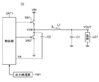
- FIG. 1 is a diagram showing a configuration of a switching power supply device according to the first embodiment.
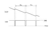
- FIG. 2 is a time chart showing the operation of the switching power supply device according to the first embodiment.
- FIG. 3 is a diagram showing a configuration of a switching power supply device according to a second embodiment.
- FIG. 4 is a time chart showing the operation of the switching power supply device according to the second embodiment.
- FIG. 5 is a diagram showing a configuration of a switching power supply device according to a third embodiment.
- FIG. 6 is a time chart showing the operation of the switching power supply device according to the third embodiment.
- FIG. 7 is a diagram showing a configuration of a switching power supply device according to a fourth embodiment.
- FIG. 8 is a time chart showing the operation of the switching power supply device according to the fourth embodiment.
- FIG. 9 is a diagram showing a configuration example of the switching power supply device according to the fifth embodiment.
- FIG. 10 is a time chart showing an operation example of the switching power supply device according to the fifth embodiment when an overshoot of the output voltage occurs.
- FIG. 11 is a diagram showing a state in which the inductor current is regenerated.
- FIG. 12 is a time chart of the load current.
- FIG. 13 is a time chart showing another operation example of the switching power supply device according to the fifth embodiment when an overshoot of the output voltage occurs.
- FIG. 14 is a diagram showing a state in which the inductor current is regenerated.
- FIG. 15 is a diagram showing a state in which the inductor current flows from the ground to the inductor through the body diode of the second switch.
- FIG. 16 is a waveform diagram of the inductor current and the switch voltage.
- FIG. 17 is a diagram showing a state in which the inductor current is regenerated.
- FIG. 18 is a diagram showing a state in which the inductor current flows from the inductor to the application end of the input voltage via the body diode of the first switch.
- FIG. 19 is a waveform diagram of the inductor current and the switch voltage.
- FIG. 20 is an external view showing an example of a vehicle configuration.
- a MOS transistor is a semiconductor whose gate structure is "a layer made of a semiconductor such as a conductor or a semiconductor having a small resistance value", an “insulating layer”, and a "P-type, N-type, or intrinsic semiconductor".
- FIG. 1 is a diagram showing a configuration of a switching power supply device according to the first embodiment.
- the switching power supply device 1A (hereinafter referred to as “switching power supply device 1A”) according to the first embodiment is a switching power supply device that steps down the input voltage VIN to the output voltage VOUT, and includes a control unit CNT1 and a first switch SW1.
- a second switch SW2, an inductor L1, an output capacitor C1, and an output feedback unit FB1 are provided.
- the switching power supply device 1A may be configured to operate in the current continuous mode when the load is light, or may have a backflow prevention function and operate in the current discontinuous mode when the load is light.
- the control unit CNT1 controls on / off of the first switch SW1 and the second switch SW2 based on the output of the output feedback unit FB1.
- the control unit CNT1 is a switch control device that controls on / off of the first switch SW1 and the second switch SW2.
- the first switch SW1 is configured so that the first end can be connected to the application end of the input voltage VIN and the second end can be connected to the first end of the inductor L1.
- the first switch SW1 conducts / cuts off the current path from the application end of the input voltage VIN to the inductor L1.
- a P-channel type MOS transistor, an N-channel type MOS transistor, or the like can be used as the first switch SW1 for example.
- a bootstrap circuit or the like may be provided in the switching power supply device 1A in order to generate a voltage larger than the input voltage VIN.
- the second switch SW2 is configured so that the first end can be connected to the first end of the inductor L1 and the second end of the first switch SW1 and the second end can be connected to the application end of the ground potential.
- the second switch SW2 conducts / cuts off the current path from the application end of the ground potential to the inductor L1.
- an N-channel type MOS transistor or the like can be used as the second switch SW2 for example.
- a pulsed switch voltage VSW is generated at the connection node of the first switch SW1 and the second switch SW2.
- the inductor L1 and the output capacitor C1 smooth the pulsed switch voltage VSW to generate an output voltage VOUT, and supply the output voltage VOUT to the application end of the output voltage VOUT.
- a load LD1 is connected to the application end of the output voltage VOUT, and the output voltage VOUT is supplied to the load LD1.
- the output feedback unit FB1 generates and outputs a feedback signal according to the output voltage VOUT.
- the output feedback unit FB1 for example, a resistance voltage divider circuit that generates a feedback signal by resistance dividing the output voltage VOUT can be used. Further, for example, the output feedback unit FB1 may be configured to acquire the output voltage VOUT and output the output voltage VOUT itself as a feedback signal.
- the output feedback unit FB1 is configured to generate and output a feedback signal according to the current flowing through the inductor L1 (hereinafter referred to as “inductor current IL”) in addition to the feedback signal corresponding to the output voltage VOUT. May be good.
- the output feedback unit FB1 also generates a feedback signal according to the inductor current IL, so that the current mode can be controlled.
- FIG. 2 is a time chart showing the operation of the switching power supply device 1A.
- the control unit CNT1 sets the length of the first state ST1 according to the feedback signal output from the output feedback unit FB1.
- the control unit CNT1 turns the first switch SW1 into an on state and turns the second switch SW2 into an off state.
- the switch voltage VSW becomes a value obtained by adding the forward voltage of the body diode of the first switch SW1 to the input voltage VIN, and then becomes substantially the same value as the input voltage VIN.
- the inductor current IL increases with the passage of time.
- control unit CNT1 switches the control state from the first state ST1 to the second state ST2.
- the control unit CNT1 turns the first switch SW1 into an off state and turns the second switch SW2 into an on state.
- the switch voltage VSW has substantially the same value as the ground potential GND.
- the inductor current IL decreases with the passage of time.
- the control unit CNT1 ends the second state ST2 and switches the control state from the second state ST2 to the third state ST3.
- a determination unit (not shown) for determining whether or not the inductor current IL has decreased to a predetermined value may be provided separately from the control unit CNT1 or may be built in the control unit CNT1. In this embodiment, the above predetermined value is set to zero.
- the control unit CNT1 turns off the first switch SW1 and the second switch SW2.
- the connection node of the first switch SW1 and the second switch SW2 is in the high impedance state, and the switch voltage VSW has substantially the same value as the output voltage VOUT.
- the inductor current IL becomes zero.
- the periodic signal S1 is a signal in which a pulse is generated with a fixed period Tfix.
- the periodic signal S1 may be a signal generated inside the control unit CNT1 or a signal generated outside the control unit CNT1 and acquired by the control unit CNT1.
- control unit CNT1 ends the third state ST3 and switches the control state from the third state ST3 to the fourth state ST4.
- the control unit CNT1 turns the first switch SW1 into an off state and turns the second switch SW2 into an on state.
- the switch voltage VSW has substantially the same value as the ground potential GND.
- the inductor current IL flows from the application end of the output voltage VOUT toward the connection node of the first switch SW1 and the second switch SW2, and the amount of current increases with the passage of time.
- the inductor current IL is regenerated. Since the regenerative energy of the inductor current IL is released when the fourth state ST4 is switched to the first state ST1, the switch voltage VSW rises sharply when the fourth state ST4 is switched to the first state ST1.
- control unit CNT1 ends the fourth state ST4 and switches the control state from the fourth state ST4 to the first state ST1.
- the control unit CNT1 repeats the first state ST1, the second state ST2, the third state ST3, and the fourth state ST4 in the fixed cycle Tfix.
- a dead time period during which both the first switch SW1 and the second switch SW2 are in the off state is set between the first state ST1 and the second state ST2, and between the fourth state ST4 and the first state ST1, respectively. It is desirable to provide it.
- the fixed period Tfix is the first state ST1, the first state ST1 and the first state.
- the dead time period provided between the two states ST2, the second state ST2, the third state ST3, the fourth state ST4, and the dead time period provided between the fourth state ST4 and the first state ST1 are totaled. Matches the period.
- the switching power supply device 1A Since the switching power supply device 1A operates in a fixed cycle Tfix and does not cause a loss in the third state ST3, high efficiency can be achieved without changing the switching frequency. Since the length of the first state ST1 becomes shorter and the length of the third state ST3 becomes longer when the load LD1 is a light load, the switching power supply unit 1A greatly improves the efficiency when the load LD1 is a light load. Can be made to.
- the second switch SW2 may be configured so that the second end can be connected to an application end having a lower voltage than the input voltage VIN and a low voltage other than the ground potential.
- FIG. 3 is a diagram showing a configuration of a switching power supply device according to a second embodiment.
- the switching power supply device 1B (hereinafter referred to as “switching power supply device 1B”) according to the second embodiment has a configuration in which a switch SW3 is added to the switching power supply device 1A.
- Switch SW3 is connected in parallel to switch SW2. That is, the first end of the switch SW3 is connected to the first end of the switch SW2, and the second end of the switch SW3 is connected to the second end of the switch SW2.
- the third switch SW3 for example, an N-channel type MOS transistor or the like can be used.
- the control unit CNT1 controls on / off of the third switch SW3 in addition to the on / off of the first switch SW1 and the second switch SW2.
- the switch SW3 has a smaller on-resistance (resistance between the first end and the second end in the on state) and a capacitance (parasitic capacitance between the first end and the second end) than the switch SW2. ..
- FIG. 4 is a time chart showing the operation of the switching power supply device 1B.
- the operation of the switching power supply device 1B is different from the operation of the switching power supply device 1A in that the control unit CNT1 turns off the second switch SW2 in the fourth state ST4.
- the control unit CNT1 turns on the third switch SW3 instead of the second switch SW2.
- the switching power supply unit 1B can make the loss in the fourth state ST4 smaller than that of the switching power supply unit 1A.
- the control unit CNT1 turns off the third switch SW3.
- the switching power supply device 1B Since the switching power supply device 1B operates in a fixed cycle Tfix and does not cause a loss in the third state ST3, high efficiency can be achieved without changing the switching frequency. Since the length of the first state ST1 becomes shorter and the length of the third state ST3 becomes longer when the load LD1 is a light load, the switching power supply unit 1B greatly improves the efficiency when the load LD1 is a light load. Can be made to.
- control unit CNT1 may turn on both the second switch SW2 and the third switch SW3.
- the second end of the second switch SW2 and the second end of the third switch SW3 are configured to be connectable to an application end having a voltage lower than the input voltage VIN and a low voltage other than the ground potential. You may.
- FIG. 5 is a diagram showing a configuration of a switching power supply device according to a third embodiment.
- the switching power supply device 1C (hereinafter referred to as “switching power supply device 1C”) according to the third embodiment has a configuration in which a switch SW3, a capacitance C2, and a switch SW4 are added to the switching power supply device 1A.
- the first end of the switch SW3 is connected to the connection node of the first switch SW1 and the second switch SW2.
- the second end of the switch SW3 is connected to the first end of the capacitance C2 and the first end of the fourth switch SW4.
- the second end of the capacitance C2 and the second end of the fourth switch SW4 are connected to the ground potential.
- As the third switch SW3, for example, an N-channel type MOS transistor or the like can be used.
- the fourth switch SW4 for example, an N-channel type MOS transistor or the like can be used.
- the control unit CNT1 controls on / off of the third switch SW3 and the fourth switch SW4 in addition to the on / off of the first switch SW1 and the second switch SW2.
- the switch SW3 has a smaller on-resistance (resistance between the first end and the second end in the on state) and a capacitance (parasitic capacitance between the first end and the second end) than the switch SW2. ..
- the switch SW3 may have the same on-resistance and capacitance as the switch SW2.
- the switch SW4 is a switch for discharging the capacitance C2. When the switch SW4 is turned on, both ends of the capacitance C2 are short-circuited and the capacitance C2 is discharged.
- FIG. 6 is a time chart showing the operation of the switching power supply device 1C.
- the operation of the switching power supply device 1C is basically the same as the operation of the switching power supply device 1B.
- on / off control of the fourth switch SW4 by the control unit CNT1 is added.
- the control unit CNT1 complementarily controls the on / off of the third switch SW3 and the on / off of the fourth switch SW4. That is, the control unit CNT1 turns on the fourth switch SW4 in the first state ST1, the second state ST2, and the third state ST3, and turns the fourth switch SW4 in the fourth state ST4.
- the switch voltage SW sets the input voltage VIN, the parasitic capacitance between the first end and the second end of the first switch SW1, and the first end of the third switch SW3.
- the voltage is divided by the parasitic capacitance and the capacitance C2 between the and the second end.
- the value of the switch voltage SW in the fourth state ST4 can be adjusted by the capacitance value of the capacitance C2. That is, the rising condition of the switch voltage VSW when switching from the fourth state ST4 to the first state ST1 can be adjusted by the capacitance value of the capacitance C2.
- control unit CNT1 in the semiconductor integrated circuit device and using the capacitance C2 as an external component of the semiconductor integrated circuit device, it becomes easy to adjust the value of the switch voltage SW in the fourth state ST4.
- the switching power supply device 1C Since the switching power supply device 1C operates in a fixed cycle Tfix and does not cause a loss in the third state ST3, high efficiency can be achieved without changing the switching frequency. Since the length of the first state ST1 becomes shorter and the length of the third state ST3 becomes longer when the load LD1 is a light load, the switching power supply unit 1C greatly improves the efficiency when the load LD1 is a light load. Can be made to.
- the second end of the second switch SW2, the second end of the capacitance C2, and the second end of the fourth switch SW4 are lower than the input voltage VIN and have a low voltage other than the ground potential. It may be configured to be connectable to the application end.
- FIG. 7 is a diagram showing a configuration of a switching power supply device according to a fourth embodiment.
- FIG. 8 is a time chart showing the operation of the switching power supply device according to the fourth embodiment.
- the switching power supply device 1D (hereinafter referred to as “switching power supply device 1D”) according to the fourth embodiment has a configuration in which a capacitance C2 is added to the switching power supply device 1A.
- the first end of the capacity C2 is connected to the connection node of the first switch SW1 and the second switch SW2.
- the control unit CNT1 controls the voltage VA applied to the second end of the switch SW3.
- the control unit CNT1 sets the voltage VA to the HIGH level (for example, the same value as the output voltage VOUT) in the third state ST3, and sets the voltage VA to the LOW level in the first state ST1, the second state ST2, and the fourth state ST4 (for example, the same value as the output voltage VOUT).
- the ground potential GND For example, the ground potential GND.
- the switching power supply device 1D Since the switching power supply device 1D operates in a fixed cycle Tfix and does not cause a loss in the third state ST3, high efficiency can be achieved without changing the switching frequency. Since the length of the first state ST1 becomes shorter and the length of the third state ST3 becomes longer when the load LD1 is a light load, the switching power supply unit 1D greatly improves the efficiency when the load LD1 is a light load. Can be made to.
- the second end of the second switch SW2 may be configured to be connectable to an application end having a voltage lower than the input voltage VIN and a low voltage other than the ground potential.
- FIG. 9 is a diagram showing a configuration example of the switching power supply device according to the fifth embodiment. It is a figure which shows the configuration example of a switching power supply device.
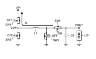
- the switching power supply device 1E (hereinafter referred to as “switching power supply device 1E”) according to the fifth embodiment of the configuration example shown in FIG. 9 is a switching power supply device that steps down the input voltage VIN to the output voltage VOUT, and is a control unit CNT1. , 1st to 4th switches SW1 to SW4, an inductor L1, an output capacitor C1, an output feedback unit FB1, and a detection unit DET1.
- the switching power supply device 1E may be configured to operate in the current continuous mode when the load is light, or may have a backflow prevention function and operate in the current discontinuous mode when the load is light.
- the control unit CNT1 controls on / off of the first to fourth switches SW1 to SW4 based on the outputs of the output feedback unit FB1 and the detection unit DET1.
- the control unit CNT1 is a switch control device that controls on / off of the first to fourth switches SW1 to SW4.
- the control unit CNT1 has an acquisition unit 2 that acquires the detection result of the detection unit DET1, and a first switch SW1, a second switch SW2, a third switch SW3, and a control unit SW3 based on the detection result of the detection unit DET1 acquired by the acquisition unit 2.
- the suppression unit 3 for suppressing the overshoot of the output voltage VOUT by turning on the switch SW3 is provided.
- the acquisition unit 2 and the suppression unit 3 may be realized by software, may be realized by a hardware circuit, or may be realized by the cooperation between the hardware and the hardware.
- the first switch SW1 is configured so that the first end can be connected to the application end of the input voltage VIN and the second end can be connected to the first end of the inductor L1.
- the first switch SW1 conducts / cuts off the current path from the application end of the input voltage VIN to the inductor L1.
- a P-channel type MOS transistor, an N-channel type MOS transistor, or the like can be used as the first switch SW1 .
- a bootstrap circuit or the like may be provided in the switching power supply device 1E in order to generate a voltage larger than the input voltage VIN.
- the second switch SW2 is configured so that the first end can be connected to the first end of the inductor L1 and the second end of the first switch SW1 and the second end can be connected to the application end of the ground potential.
- the second switch SW2 conducts / cuts off the current path from the application end of the ground potential to the inductor L1.
- the second switch SW2 may be configured so that the second end is lower than the input voltage VIN and can be connected to the application end of a voltage other than the ground potential.
- the voltage applied to the second end of the second switch SW2 is the same as the voltage applied to the second end of the third switch SW3.
- the second switch SW2 for example, an N-channel type MOS transistor or the like can be used.
- a pulsed switch voltage VSW is generated at the connection node of the first switch SW1 and the second switch SW2.
- the inductor L1 and the output capacitor C1 smooth the pulsed switch voltage VSW to generate an output voltage VOUT, and supply the output voltage VOUT to the application end of the output voltage VOUT.
- a load LD1 is connected to the application end of the output voltage VOUT, and the output voltage VOUT is supplied to the load LD1.
- the third switch SW3 is configured so that the first end can be connected to the second end of the inductor L1 and the second end can be connected to the application end of the ground potential.
- the third switch SW3 for example, an N-channel type MOS transistor or the like can be used.
- the fourth switch SW4 is configured so that the first end can be connected to the second end of the inductor L1 and the first end of the third switch, and the second end can be connected to the application end of the output voltage VOUT.
- the fourth switch SW4 for example, an N-channel type MOS transistor or the like can be used.
- the withstand voltage of the third switch SW3 and the fourth switch SW4 may be lower than the withstand voltage of the first switch SW1 and the second switch SW2. Therefore, the size of the third switch SW3 and the fourth switch SW4 can be reduced. Further, by making the third switch SW3 and the fourth switch SW4 smaller, the loss generated in each parasitic capacitance of the third switch SW3 and the fourth switch SW4 can be reduced.
- the output feedback unit FB1 generates and outputs a feedback signal according to the output voltage VOUT.
- the output feedback unit FB1 for example, a resistance voltage divider circuit that generates a feedback signal by resistance dividing the output voltage VOUT can be used. Further, for example, the output feedback unit FB1 may be configured to acquire the output voltage VOUT and output the output voltage VOUT itself as a feedback signal.
- the output feedback unit FB1 is configured to generate and output a feedback signal according to the current flowing through the inductor L1 (hereinafter referred to as “inductor current IL”) in addition to the feedback signal corresponding to the output voltage VOUT. May be good.
- the output feedback unit FB1 also generates a feedback signal according to the inductor current IL, so that the current mode can be controlled.
- the detection unit DET1 detects the occurrence and convergence of an overshoot of the output voltage VOUT.
- a comparator that inputs the output voltage VOUT to the non-inverting input terminal and inputs a constant voltage (a voltage larger than the target value of the output voltage VOUT) to the inverting input terminal can be used.
- the comparator switches the output signal from low level to high level when an overshoot of the output voltage VOUT occurs.
- the comparator switches the output signal from high level to low level when the overshoot of the output voltage VOUT converges.
- FIG. 10, which will be described later, illustrates this exemplary output signal.
- the divided voltage of the output voltage VOUT may be input to the non-inverting input terminal of the comparator instead of the output voltage VOUT, and the divided voltage of the constant voltage may be input to the inverting input terminal of the comparator instead of the constant voltage.
- the value of the output voltage VOUT at the time of detecting the occurrence of overshoot and the overshoot convergence detection are detected.
- the value of the output voltage VOUT at the time point can be different from each other.
- the detection unit DET1 does not necessarily have to detect the convergence of the overshoot of the output voltage VOUT. For example, when a counter is provided in the control unit CNT1 and a certain period of time measured by the counter elapses from the time when the detection unit DET1 detects the occurrence of an overshoot of the output voltage VOUT, the control unit CNT1 causes the overshoot of the output voltage VOUT to occur. It may be determined that it has converged.
- the detection unit DET1 detects a sign of an overshoot of the output voltage VOUT and the detection unit DET1 detects a sign of an overshoot of the output voltage VOUT
- the above-mentioned suppression The unit 3 may turn off the first switch SW1 and the second switch SW2 and turn on the third switch SW3 to suppress the overshoot of the output voltage VOUT.
- FIG. 10 is a time chart showing an operation example of the switching power supply device 1E when an overshoot of the output voltage VOUT occurs.
- the switching power supply device 1E When the occurrence of overshoot of the output voltage VOUT is detected by the detection unit DET1, the switching power supply device 1E becomes the second state START2 under the control of the control unit CNT1.
- the occurrence of an overshoot of the output voltage VOUT is detected by the detection unit DET1 in the middle of the first state START1 (in the middle of the on-duty period of the switch SW), and the output of the detection unit DET1 changes from low level to high level.
- the first switch SW1 and the fourth switch SW4 In the first state START1, the first switch SW1 and the fourth switch SW4 are in the on state, and the second switch SW2 and the third switch SW3 are in the off state under the control of the control unit CNT1.
- the first switch SW1 and the fourth switch SW4 are turned off, and the second switch SW2 and the third switch SW3 are turned on under the control of the control unit CNT1.
- the inductor current IL is closed including the second switch SW2, the inductor L1 and the third switch SW3 as shown in FIG. Regenerate in the circuit.
- the current supply to the load LD1 side can be cut off.
- the fourth switch SW4 since the fourth switch SW4 is in the off state, the output voltage VOUT can be substantially clamped near the level at the time of overshoot occurrence.
- the output voltage VOUT is further increased by turning off the first switch SW1 and the fourth switch SW4 and turning on the second switch SW2 and the third switch SW3 when the overshoot of the output voltage VOUT occurs. It can be prevented and overshoot of the output voltage VOUT can be suppressed.
- the state of the switching power supply device 1E is maintained in the second state START2 until the convergence of the overshoot of the output voltage VOUT is detected by the detection unit DET1. While the second state START2 is maintained, the inductor current IL gradually decreases due to the on-resistance of the second switch SW2 and the on-resistance of the third switch SW3.
- the state of the switching power supply device 1E is changed from the second state STATE2 to the first state.
- the transition to START1 is made, but this transition is merely an example. That is, after the end of the second state START2, the state may be changed to a state other than the first state START1.
- the second state START2 is maintained without being interrupted from the occurrence of the overshoot of the output voltage VOUT to the convergence.
- the second state START 2 may be temporarily interrupted between the occurrence of the overshoot of the output voltage VOUT and the convergence. The second state START 2 may be terminated without waiting for the overshoot of the output voltage VOUT to converge.
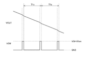
- FIG. 13 is a time chart showing other operations of the switching power supply device 1E when an overshoot of the output voltage VOUT occurs.
- the switching power supply device 1E When the occurrence of overshoot of the output voltage VOUT is detected by the detection unit DET1, the switching power supply device 1E becomes the second state START2 under the control of the control unit CNT1.
- the occurrence of an overshoot of the output voltage VOUT is detected by the detection unit DET1 in the middle of the first state START1 (during the on-duty period of the switch voltage VSW), and the output of the detection unit DET1 is from low level to high level. It is a time chart when the state of the switching power supply device 1E changes from the first state START1 to the second state START2.
- the first switch SW1 and the second switch SW2 complementarily switch between the on state and the off state with the fixed cycle Tfix based on the periodic signal S1 under the control of the control unit CNT1, and the third switch SW3 is turned off.
- the state is set, and the fourth switch SW4 is in the ON state.
- the periodic signal S1 is a signal in which a pulse is generated with a fixed period Tfix.
- the periodic signal S1 may be a signal generated inside the control unit CNT1 or a signal generated outside the control unit CNT1 and acquired by the control unit CNT1. It is desirable to provide a dead time period in which both the first switch SW1 and the second switch SW2 are in the off state when the first switch SW1 and the second switch SW2 are complementarily switched between the on state and the off state.
- the first switch SW1 is turned off by the control of the control unit CNT1, and the on state and the off state of the second to fourth switches SW2 to SW4 are switched in the fixed cycle Tfix.
- the second switch SW2, the third switch SW3, and the fourth switch SW4 complementarily switch between the on state and the off state with a fixed cycle Tfix.
- the control unit CNT1 switches between the on state and the off state of the second to fourth switches SW2 to SW4 based on the periodic signal S1.
- the state START 2-1 is a period in which the second switch SW2 and the third switch SW3 are in the on state and the fourth switch SW4 is in the off state
- the state START 2-2 is a state in which the second switch SW2 and the third switch SW3 are in the off state. This is the period during which the fourth switch SW4 is in the ON state.
- the state of the switching power supply device 1E is maintained in the second state START2 until the convergence of the overshoot of the output voltage VOUT is detected by the detection unit DET1. While the second state START2 is maintained, the inductor current IL gradually decreases due to the on-resistance of the second switch SW2 and the on-resistance of the third switch SW3.
- the state of the switching power supply device 1E is changed from the second state STATE2 to the third state. Transition to START3.
- the first to third switches SW1 to SW3 are turned off and the fourth switch SW4 is turned on by the control of the control unit CNT1.
- the details of the state STATE2-1 and the state START2-2 will be described by taking as an example the case where the N-channel type MOS transistor is used for the first to fourth switches SW1 to SW4.
- bipolar transistors may be used for the first to fourth switches SW1 to SW4, and a "reverse connection diode" may be connected in parallel to each bipolar transistor.
- the direction in which the current of the "reverse connection diode” flows is opposite to the direction in which the current of the bipolar transistor connected in parallel to the "reverse connection diode" flows.
- the inductor current IL is closed including the second switch SW2, the inductor L1, and the third switch SW3. It regenerates in the circuit, and the switch voltage SW and the ground potential become substantially the same.
- the fourth switch SW4 since the fourth switch SW4 is in the off state, the current supply to the load LD1 side can be cut off. Therefore, the output voltage VOUT can be substantially clamped to the vicinity of the level at the time of overshoot occurrence. That is, the output voltage VOUT is further increased by turning off the first switch SW1 and the fourth switch SW4 and turning on the second switch SW2 and the third switch SW3 when the overshoot of the output voltage VOUT occurs. It can be prevented and overshoot of the output voltage VOUT can be suppressed.
- the period of each state START2-2 is a fixed period. Specifically, the period of each state STATE2-2 is a fixed period corresponding to the pulse width of the periodic signal S1. It is desirable that the period of each state STATE2-2 is 1/10 or less of the fixed period Tfix. This is because when the period of each state START2-2 is longer than 1/10 of the fixed period Tfix, the time required for the overshoot of the output voltage VOUT to converge exceeds the allowable range.
- the output voltage VOUT and the switch voltage VSW in the second state START are as shown in FIG. It should be noted that the output voltage VOUT is enlarged with respect to the switch voltage VSW with respect to the scale in the vertical direction of the paper surface of FIG.
- the cycle of the switch voltage VSW is a fixed cycle Tfix. That is, since the frequency (switching frequency) of the switch voltage VSW does not fluctuate, the frequency of noise caused by the switching frequency also does not fluctuate. Therefore, there is no possibility that the effect of the noise suppressing means (for example, a filter circuit) for suppressing the noise of a fixed frequency is reduced.
- the inductor current IL is closed including the second switch SW2, the inductor L1, and the third switch SW3. It regenerates in the circuit, and the switch voltage SW and the ground potential become substantially the same.
- the fourth switch SW4 since the fourth switch SW4 is in the off state, the current supply to the load LD1 side can be cut off. Therefore, the output voltage VOUT can be substantially clamped to the vicinity of the level at the time of overshoot occurrence. That is, the output voltage VOUT is further increased by turning off the first switch SW1 and the fourth switch SW4 and turning on the second switch SW2 and the third switch SW3 when the overshoot of the output voltage VOUT occurs. It can be prevented and overshoot of the output voltage VOUT can be suppressed.
- the inductor current IL is from the inductor L1 to the input voltage VIN via the body diode of the first switch SW1. It flows toward the application end. Therefore, the switch voltage VSW becomes VIN + Vf SW1 . Note that Vf SW1 is the forward voltage of the body diode of the first switch SW1.
- the output voltage VOUT and the switch voltage VSW in the second state START are as shown in FIG. It should be noted that the output voltage VOUT is enlarged with respect to the switch voltage VSW with respect to the scale in the vertical direction of the paper in FIG. As can be seen from FIG. 19, the cycle of the switch voltage VSW is a fixed cycle Tfix. That is, since the frequency (switching frequency) of the switch voltage VSW does not fluctuate, the frequency of noise caused by the switching frequency also does not fluctuate. Therefore, there is no possibility that the effect of the noise suppressing means (for example, a filter circuit) for suppressing the noise of a fixed frequency is reduced.
- the noise suppressing means for example, a filter circuit
- control unit CNT1 may turn on the second switch SW2 in the state START2-2. Further, when the inductor current IL is in the negative direction, unlike this operation example, the control unit CNT1 may turn on the first switch SW1 in the state START2-2.
- the set value of the fixed cycle Tfix may be changeable. By changing the cycle of the cycle signal S1, the set value of the fixed cycle Tfix can be changed.
- FIG. 9 is an external view showing a configuration example of a vehicle equipped with an in-vehicle device.
- the vehicle X of this configuration example is equipped with in-vehicle devices X11 to X17 and a battery (not shown) for supplying electric power to these in-vehicle devices X11 to X17.
- the control unit CNT1 When any of the switching power supply devices 1A to 1E described above is mounted on the vehicle X, it is required to suppress the radiation noise in the AM band so that the reception of the AM radio broadcast is not adversely affected. Therefore, it is desirable that the control unit CNT1 generate a voltage of 1.8 MHz or more and 2.1 MHz or less at the connection node of the first switch SW1 and the second switch SW2. That is, it is desirable that the control unit CNT1 sets the frequency (switching frequency) of the switch voltage VSW to 1.8 MHz or more and 2.1 MHz or less. This is because when the switching frequency is less than 1.8 MHz, the radiation noise in the AM band increases, and when the switching frequency is larger than 2.1 MHz, the switching loss exceeds the allowable range.
- the in-vehicle device X11 is an engine control unit that performs control related to the engine (injection control, electronic throttle control, idling control, oxygen sensor heater control, auto cruise control, etc.).
- the in-vehicle device X12 is a lamp control unit that controls turning on and off such as HID [high intensity discharged lamp] and DRL [daytime running lamp].
- the in-vehicle device X13 is a transmission control unit that performs control related to the transmission.
- the in-vehicle device X14 is a body control unit that performs control related to the movement of the vehicle X (ABS [anti-lock brake system] control, EPS [electric power steering] control, electronic suspension control, etc.).
- ABS anti-lock brake system
- EPS electric power steering
- electronic suspension control etc.
- the in-vehicle device X15 is a security control unit that controls the drive of door locks, security alarms, and the like.
- the in-vehicle device X16 is an electronic device incorporated in the vehicle X at the factory shipment stage as a standard equipment or a manufacturer's option such as a wiper, an electric door mirror, a power window, an electric sunroof, an electric seat, and an air conditioner.
- the in-vehicle device X17 is an electronic device that is arbitrarily attached to the vehicle X by the user, such as an in-vehicle A / V [audio / visual] device, a car navigation system, and an ETC [Electronic Toll Collection System].
- the switching power supply devices 1A to 1E described above can be incorporated into any of the in-vehicle devices X11 to X17, respectively.
- the set value of the fixed cycle Tfix may be changeable. By changing the cycle of the cycle signal S1, the set value of the fixed cycle Tfix can be changed.
- the integrated circuit package incorporating the first switch SW1 and the second switch SW2 and the integrated circuit package since the third switch SW4 and the fourth switch SW4 have a lower withstand voltage than the first switch SW1 and the second switch SW2, the integrated circuit package incorporating the first switch SW1 and the second switch SW2 and the integrated circuit package. It is preferable to make the integrated circuit package containing the third switch SW3 and the fourth switch SW4 into separate integrated circuit packages. As a result, each integrated circuit package can be efficiently designed and manufactured.
- first to fourth switches SW1 to SW4 may be built in the same integrated circuit package. Further, the first to fourth switches SW1 to SW4 may be discrete parts.
- the switching power supply device is a switching power supply device configured to step down the input voltage to the output voltage, and the first end is configured to be connectable to the application end of the input voltage.
- the first switch is configured so that the second end can be connected to the first end of the inductor, and the first end is configured to be connectable to the first end of the inductor and the second end of the first switch.
- a second switch configured to be connectable to an application end having a voltage lower than the input voltage, and a control unit configured to control the on / off of the first switch and the second switch.
- the control unit turns the first switch on and turns the second switch off, and after the first state, turns the first switch off and turns the second switch on.
- the switching power supply device having the first configuration described above can improve efficiency without changing the switching frequency.
- control unit may have a configuration (second configuration) in which the first switch is turned off and the second switch is turned on in the fourth state.
- the switching power supply device having the second configuration can regenerate the current flowing through the inductor in the fourth state.
- the control unit includes a third switch which is configured to be connectable to the second switch in parallel and has at least one of the on-resistance and the capacitance smaller than that of the second switch. Is configured to control the on / off of the third switch, and the control unit has a configuration in which the first switch is turned off and the third switch is turned on in the fourth state (third state). Configuration) may be used.
- the switching power supply device having the third configuration can reduce the loss in the fourth state.
- the first end is a third switch configured to be connectable to the first end of the inductor and the second end of the first switch, and the first end is the third switch.
- the control unit is configured to control on / off of the third switch.
- the control unit may be configured to turn off the first switch and turn on the third switch in the fourth state (fourth configuration).
- the rise of the switch voltage generated in the connection node of the first switch and the second switch when the fourth state is switched to the first state according to the capacitance value of the capacitance. Can be adjusted.
- the switching power supply device having the fourth configuration includes a fourth switch configured to be connectable in parallel to the capacitance, and the control unit is configured to control on / off of the fourth switch. May have a configuration (fifth configuration) in which the on / off of the third switch and the on / off of the fourth switch are controlled in a complementary manner.
- the switching power supply device having the fifth configuration described above can discharge the capacity at an appropriate timing.
- the first end is configured to be connectable to the first end of the inductor and the second end of the first switch, and the second end is connectable to the end to which a variable voltage is applied.
- the control unit is configured to control the variable voltage, and the control unit turns off the first switch in the fourth state and controls the variable voltage to control the capacity.
- a configuration (sixth configuration) may be used in which a potential difference is generated between the first end and the second end.
- the switching power supply device having the sixth configuration is generated at the connection node of the first switch and the second switch when the fourth state is switched to the first state by adjusting the value of the variable voltage in the fourth state.
- the rise of the switch voltage can be adjusted.
- the switching power supply device is a switching power supply device configured to step down the input voltage to the output voltage, and the first end is configured to be connectable to the application end of the input voltage.
- the first switch is configured so that the second end can be connected to the first end of the inductor, and the first end is configured to be connectable to the first end of the inductor and the second end of the first switch. Is configured to be connectable to the application end of a low voltage lower than the input voltage, and the first end is configured to be connectable to the second end of the inductor, and the second end is the application of the low voltage.
- a third switch that can be connected to the end, a first end that can be connected to the second end of the inductor and the first end of the third switch, and the second end to the application end of the output voltage.
- a fourth switch configured to be connectable, a detection unit configured to detect the occurrence or a sign of overshoot of the output voltage, the first switch, the second switch, the third switch, and the said.
- the control unit includes a control unit configured to control the on / off of the fourth switch, and when the detection unit detects the occurrence or a sign of overshoot of the output voltage, the first control unit.
- the configuration is such that the switch and the fourth switch are turned off, and the second switch and the third switch are turned on (seventh configuration).
- the switching power supply device having the seventh configuration can suppress overshoot of the output voltage.
- the detection unit also detects the convergence of the overshoot of the output voltage, and the control unit detects the convergence of the overshoot of the output voltage by the detection unit.
- the third switch may be turned off and the fourth switch may be turned on (eighth configuration).
- the switching power supply device having the eighth configuration can reliably suppress the overshoot of the output voltage until the overshoot of the output voltage converges.
- the detection unit in the control unit, after the detection unit detects the occurrence or a sign of the overshoot of the output voltage, the detection unit converges the overshoot of the output voltage.
- the first switch and the fourth switch are turned off, and the second switch is turned on and the third switch is used.
- a configuration (9th configuration) may be used in which the on state, the off state of the second switch, and the off state of the third switch are switched at a fixed cycle.
- the switching power supply device having the ninth configuration can suppress fluctuations in the noise frequency.
- the off state period of the second switch and the third switch may be a fixed period (tenth configuration).
- the switching power supply device having the tenth configuration can stably suppress output voltage overshoot every cycle.
- the off state period of the second switch and the third switch may be 1/10 or less of the fixed cycle (11th configuration).
- the switching power supply device having the eleventh configuration can prevent the time required for the overshoot of the output voltage to converge from exceeding the allowable range.
- the switching power supply device having the twelfth configuration can suppress radiation noise and switching loss in the AM band.
- the first switch is configured so that the first end can be connected to the application end of the input voltage and the second end can be connected to the first end of the inductor. On / off, the first end can be connected to the first end of the inductor and the second end of the first switch, and the second end can be connected to the application end of a low voltage lower than the input voltage.
- a switch control device that controls the on / off of the configured second switch, the first state in which the first switch is turned on and the second switch is turned off, and the first state.
- the third state After the third state, it has a fourth state in which the voltage of the connection node between the first switch and the second switch is lower than that in the third state, and the first state and the second state have a fixed cycle. It is a configuration (13th configuration) in which the state, the third state, and the fourth state are repeated.
- the switch control device having the thirteenth configuration can improve the efficiency of the switching power supply device equipped with the switch control device without changing the switching frequency of the switching power supply device equipped with the switch control device.
- the first switch is configured so that the first end can be connected to the application end of the input voltage and the second end can be connected to the first end of the inductor.
- the first end can be connected to the first end of the inductor and the second end of the first switch, and the second end can be connected to the application end of a low voltage lower than the input voltage.
- the third switch configured so that the first end can be connected to the second end of the inductor and the second end can be connected to the low voltage application end.
- a fourth switch configured so that the first end can be connected to the second end of the inductor and the first end of the third switch, and the second end can be connected to the applied end of the output voltage.
- a switch control device that controls the on / off of the output voltage, the acquisition unit configured to acquire the detection result of the detection unit that detects the occurrence or sign of overshoot of the output voltage, and the acquisition unit.
- the on / off of the first switch, the second switch, the third switch, and the fourth switch is controlled based on the acquired detection result, and the detection unit causes the overshoot of the output voltage or a sign thereof.
- the first switch and the fourth switch are turned off, and the second switch and the third switch are turned on to suppress the overshoot of the output voltage. (14th configuration).
- the switch control device having the above 14th configuration can suppress overshoot of the output voltage.
- the in-vehicle device described above has a configuration (15th configuration) including a switching power supply device having any one of the first to twelfth configurations or a switch control device having the thirteenth or fourteenth configuration.
- the vehicle-mounted device having the fifteenth configuration is intended to improve the efficiency of the switching power supply device mounted on the vehicle-mounted device without changing the switching frequency of the switching power supply device mounted on the vehicle-mounted device, or the vehicle-mounted device. It is possible to suppress overshoot of the output voltage of the switching power supply device mounted on the in-vehicle device.
- the vehicle described above has a configuration (sixteenth configuration) including an in-vehicle device having the fifteenth configuration and a battery for supplying electric power to the in-vehicle device.
- the efficiency of the switching power supply device mounted on the vehicle can be improved without changing the switching frequency of the switching power supply device mounted on the vehicle, or the in-vehicle device can be used. It is possible to suppress overshoot of the output voltage of the mounted switching power supply device.
- Switching power supply device 1A to 1E Switching power supply device according to the first to fifth embodiments 2 Acquisition unit 3 Suppression unit C1 Output capacitor C2 Capacity CNT1 Control unit DET1 Detection unit FB1 Output feedback unit L1 Inductor LD1 Load SW1 to SW4 1st to 4th switches X Vehicle X11-X17 In-vehicle equipment
Landscapes
- Engineering & Computer Science (AREA)
- Power Engineering (AREA)
- Dc-Dc Converters (AREA)
Priority Applications (4)
| Application Number | Priority Date | Filing Date | Title |
|---|---|---|---|
| DE112021001970.8T DE112021001970T5 (de) | 2020-06-04 | 2021-05-28 | Schaltnetzteilvorrichtung, schaltersteuergerät, fahrzeugmontiertes gerät und fahrzeug |
| JP2022528789A JPWO2021246302A1 (https=) | 2020-06-04 | 2021-05-28 | |
| CN202180039687.8A CN115943548A (zh) | 2020-06-04 | 2021-05-28 | 开关电源装置、开关控制装置、车载设备和车辆 |
| US17/925,529 US20230198397A1 (en) | 2020-06-04 | 2021-05-28 | Switching power supply device, switch control device, vehicle-mounted appliance, and vehicle |
Applications Claiming Priority (4)
| Application Number | Priority Date | Filing Date | Title |
|---|---|---|---|
| JP2020097976 | 2020-06-04 | ||
| JP2020-097976 | 2020-06-04 | ||
| JP2020-097977 | 2020-06-04 | ||
| JP2020097977 | 2020-06-04 |
Publications (1)
| Publication Number | Publication Date |
|---|---|
| WO2021246302A1 true WO2021246302A1 (ja) | 2021-12-09 |
Family
ID=78831117
Family Applications (1)
| Application Number | Title | Priority Date | Filing Date |
|---|---|---|---|
| PCT/JP2021/020345 Ceased WO2021246302A1 (ja) | 2020-06-04 | 2021-05-28 | スイッチング電源装置、スイッチ制御装置、車載機器、及び車両 |
Country Status (5)
| Country | Link |
|---|---|
| US (1) | US20230198397A1 (https=) |
| JP (1) | JPWO2021246302A1 (https=) |
| CN (1) | CN115943548A (https=) |
| DE (1) | DE112021001970T5 (https=) |
| WO (1) | WO2021246302A1 (https=) |
Families Citing this family (1)
| Publication number | Priority date | Publication date | Assignee | Title |
|---|---|---|---|---|
| CN118339754A (zh) * | 2021-12-03 | 2024-07-12 | 罗姆股份有限公司 | 开关电源装置、开关控制装置、车载设备和车辆 |
Citations (5)
| Publication number | Priority date | Publication date | Assignee | Title |
|---|---|---|---|---|
| JP2002281743A (ja) * | 2001-03-19 | 2002-09-27 | Hitachi Ltd | 半導体集積回路および携帯用電子機器 |
| JP2004248374A (ja) * | 2003-02-12 | 2004-09-02 | Fuji Electric Device Technology Co Ltd | スイッチングレギュレータ |
| US20070085520A1 (en) * | 2005-06-17 | 2007-04-19 | Via Technologies, Inc. | A pulse-frequency mode dc-dc converter circuit |
| US20140300329A1 (en) * | 2013-03-15 | 2014-10-09 | Maxim Integrated Products, Inc. | Systems and Methods to Auto-Adjust Zero Cross Circuits for Switching Regulators |
| JP2016032320A (ja) * | 2014-07-28 | 2016-03-07 | ローム株式会社 | スイッチング電源装置 |
Family Cites Families (19)
| Publication number | Priority date | Publication date | Assignee | Title |
|---|---|---|---|---|
| US6271651B1 (en) | 2000-04-20 | 2001-08-07 | Volterra Semiconductor Corporation | Inductor shorting switch for a switching voltage regulator |
| JP2004015974A (ja) * | 2002-06-11 | 2004-01-15 | Tdk Corp | スイッチング電源装置 |
| JP4017490B2 (ja) * | 2002-10-02 | 2007-12-05 | 株式会社デンソー | Dc/dcコンバータ |
| US7652457B2 (en) * | 2005-09-30 | 2010-01-26 | St-Ericsson Sa | Switching regulator circuit including an inductor shunt switch |
| KR100912945B1 (ko) * | 2007-04-16 | 2009-08-20 | (주)제이디에이테크놀로지 | 직류/직류 변환기 |
| JP4613986B2 (ja) | 2008-07-28 | 2011-01-19 | 日本テキサス・インスツルメンツ株式会社 | スイッチング電源装置 |
| JP2011072101A (ja) * | 2009-09-25 | 2011-04-07 | Rohm Co Ltd | 電流モード型スイッチングレギュレータ |
| US8779745B2 (en) * | 2010-03-01 | 2014-07-15 | National Semiconductor Corporation | Three-quarter bridge power converters for wireless power transfer applications and other applications |
| US9178420B1 (en) * | 2012-08-06 | 2015-11-03 | Maxim Integrated Products, Inc. | Inductive bypass, storage and release improves buck response |
| US9859793B2 (en) * | 2014-01-07 | 2018-01-02 | Endura Technologies LLC | Switched power stage with inductor bypass and a method for controlling same |
| JP6361479B2 (ja) * | 2014-02-07 | 2018-07-25 | 株式会社デンソー | 電力変換装置 |
| JP6115493B2 (ja) * | 2014-02-17 | 2017-04-19 | 株式会社デンソー | 電力変換装置 |
| JP2016032319A (ja) * | 2014-07-28 | 2016-03-07 | ローム株式会社 | スイッチング電源装置 |
| US9762124B2 (en) * | 2014-08-13 | 2017-09-12 | Endura Technologies LLC | Integrated thermal and power control |
| US9461543B2 (en) * | 2014-12-01 | 2016-10-04 | Endura Technologies LLC | DC-DC converter with digital current sensing |
| JP6815127B2 (ja) * | 2015-09-08 | 2021-01-20 | ローム株式会社 | Dc/dcコンバータ、スイッチング電源装置 |
| JP6594199B2 (ja) * | 2015-12-28 | 2019-10-23 | ローム株式会社 | スイッチングレギュレータ |
| JP6744781B2 (ja) * | 2016-08-10 | 2020-08-19 | ローム株式会社 | スイッチングレギュレータ及び集積回路パッケージ |
| JP2018148725A (ja) * | 2017-03-07 | 2018-09-20 | 株式会社オートネットワーク技術研究所 | 直流電圧変換装置 |
-
2021
- 2021-05-28 US US17/925,529 patent/US20230198397A1/en not_active Abandoned
- 2021-05-28 WO PCT/JP2021/020345 patent/WO2021246302A1/ja not_active Ceased
- 2021-05-28 CN CN202180039687.8A patent/CN115943548A/zh active Pending
- 2021-05-28 DE DE112021001970.8T patent/DE112021001970T5/de not_active Ceased
- 2021-05-28 JP JP2022528789A patent/JPWO2021246302A1/ja active Pending
Patent Citations (5)
| Publication number | Priority date | Publication date | Assignee | Title |
|---|---|---|---|---|
| JP2002281743A (ja) * | 2001-03-19 | 2002-09-27 | Hitachi Ltd | 半導体集積回路および携帯用電子機器 |
| JP2004248374A (ja) * | 2003-02-12 | 2004-09-02 | Fuji Electric Device Technology Co Ltd | スイッチングレギュレータ |
| US20070085520A1 (en) * | 2005-06-17 | 2007-04-19 | Via Technologies, Inc. | A pulse-frequency mode dc-dc converter circuit |
| US20140300329A1 (en) * | 2013-03-15 | 2014-10-09 | Maxim Integrated Products, Inc. | Systems and Methods to Auto-Adjust Zero Cross Circuits for Switching Regulators |
| JP2016032320A (ja) * | 2014-07-28 | 2016-03-07 | ローム株式会社 | スイッチング電源装置 |
Also Published As
| Publication number | Publication date |
|---|---|
| CN115943548A (zh) | 2023-04-07 |
| DE112021001970T5 (de) | 2023-01-19 |
| US20230198397A1 (en) | 2023-06-22 |
| JPWO2021246302A1 (https=) | 2021-12-09 |
Similar Documents
| Publication | Publication Date | Title |
|---|---|---|
| US11848611B2 (en) | Switching power supply device | |
| JP6307401B2 (ja) | 電流モード制御型スイッチング電源装置 | |
| JP7037637B2 (ja) | スイッチング制御回路 | |
| JP2021150990A (ja) | 過電流保護回路 | |
| CN105450016A (zh) | 电流模式控制型开关电源装置 | |
| CN114041262B (zh) | 开关电源装置 | |
| WO2021246302A1 (ja) | スイッチング電源装置、スイッチ制御装置、車載機器、及び車両 | |
| US20240322690A1 (en) | Switching power supply device, switch control device, vehicle-mounted appliance, and vehicle | |
| US20230179097A1 (en) | Switching Power Device | |
| JP2019213317A (ja) | 半導体装置 | |
| JP6967421B2 (ja) | スイッチ装置 | |
| JP2017077138A (ja) | 半導体装置 | |
| US20240313652A1 (en) | Switching power supply device, switch control device, vehicle-mounted appliance, and vehicle | |
| JP2018088828A (ja) | 電流モード制御型スイッチング電源装置 | |
| US11606033B2 (en) | Switching power supply device | |
| JP2023083100A (ja) | スイッチング電源装置 | |
| JP2023083099A (ja) | スイッチング電源装置 | |
| WO2022190856A1 (ja) | スイッチング電源装置、スイッチ制御装置、車載機器、及び車両 | |
| JP2018088830A (ja) | 電流モード制御型スイッチング電源装置 | |
| WO2022190855A1 (ja) | スイッチング電源装置、スイッチ制御装置、車載機器、及び車両 | |
| WO2023157611A1 (ja) | 駆動制御装置、車載電源システム、および車両 | |
| JP6449502B2 (ja) | 電流モード制御型スイッチング電源装置 | |
| JP6553226B2 (ja) | 電流モード制御型スイッチング電源装置 | |
| JP6473253B2 (ja) | 電流モード制御型スイッチング電源装置 | |
| CN118947053A (zh) | 驱动装置、开关电源装置以及车辆 |
Legal Events
| Date | Code | Title | Description |
|---|---|---|---|
| 121 | Ep: the epo has been informed by wipo that ep was designated in this application |
Ref document number: 21818060 Country of ref document: EP Kind code of ref document: A1 |
|
| ENP | Entry into the national phase |
Ref document number: 2022528789 Country of ref document: JP Kind code of ref document: A |
|
| 122 | Ep: pct application non-entry in european phase |
Ref document number: 21818060 Country of ref document: EP Kind code of ref document: A1 |