WO2021246302A1 - Switching power supply device, switch control device, vehicle-mounted apparatus, and vehicle - Google Patents
Switching power supply device, switch control device, vehicle-mounted apparatus, and vehicle Download PDFInfo
- Publication number
- WO2021246302A1 WO2021246302A1 PCT/JP2021/020345 JP2021020345W WO2021246302A1 WO 2021246302 A1 WO2021246302 A1 WO 2021246302A1 JP 2021020345 W JP2021020345 W JP 2021020345W WO 2021246302 A1 WO2021246302 A1 WO 2021246302A1
- Authority
- WO
- WIPO (PCT)
- Prior art keywords
- switch
- state
- power supply
- switching power
- connectable
- Prior art date
Links
Images


Classifications
-
- H—ELECTRICITY
- H02—GENERATION; CONVERSION OR DISTRIBUTION OF ELECTRIC POWER
- H02M—APPARATUS FOR CONVERSION BETWEEN AC AND AC, BETWEEN AC AND DC, OR BETWEEN DC AND DC, AND FOR USE WITH MAINS OR SIMILAR POWER SUPPLY SYSTEMS; CONVERSION OF DC OR AC INPUT POWER INTO SURGE OUTPUT POWER; CONTROL OR REGULATION THEREOF
- H02M3/00—Conversion of dc power input into dc power output
- H02M3/02—Conversion of dc power input into dc power output without intermediate conversion into ac
- H02M3/04—Conversion of dc power input into dc power output without intermediate conversion into ac by static converters
- H02M3/10—Conversion of dc power input into dc power output without intermediate conversion into ac by static converters using discharge tubes with control electrode or semiconductor devices with control electrode
- H02M3/145—Conversion of dc power input into dc power output without intermediate conversion into ac by static converters using discharge tubes with control electrode or semiconductor devices with control electrode using devices of a triode or transistor type requiring continuous application of a control signal
- H02M3/155—Conversion of dc power input into dc power output without intermediate conversion into ac by static converters using discharge tubes with control electrode or semiconductor devices with control electrode using devices of a triode or transistor type requiring continuous application of a control signal using semiconductor devices only
- H02M3/156—Conversion of dc power input into dc power output without intermediate conversion into ac by static converters using discharge tubes with control electrode or semiconductor devices with control electrode using devices of a triode or transistor type requiring continuous application of a control signal using semiconductor devices only with automatic control of output voltage or current, e.g. switching regulators
- H02M3/158—Conversion of dc power input into dc power output without intermediate conversion into ac by static converters using discharge tubes with control electrode or semiconductor devices with control electrode using devices of a triode or transistor type requiring continuous application of a control signal using semiconductor devices only with automatic control of output voltage or current, e.g. switching regulators including plural semiconductor devices as final control devices for a single load
-
- H—ELECTRICITY
- H02—GENERATION; CONVERSION OR DISTRIBUTION OF ELECTRIC POWER
- H02M—APPARATUS FOR CONVERSION BETWEEN AC AND AC, BETWEEN AC AND DC, OR BETWEEN DC AND DC, AND FOR USE WITH MAINS OR SIMILAR POWER SUPPLY SYSTEMS; CONVERSION OF DC OR AC INPUT POWER INTO SURGE OUTPUT POWER; CONTROL OR REGULATION THEREOF
- H02M1/00—Details of apparatus for conversion
- H02M1/0003—Details of control, feedback or regulation circuits
- H02M1/0009—Devices or circuits for detecting current in a converter
-
- H—ELECTRICITY
- H02—GENERATION; CONVERSION OR DISTRIBUTION OF ELECTRIC POWER
- H02M—APPARATUS FOR CONVERSION BETWEEN AC AND AC, BETWEEN AC AND DC, OR BETWEEN DC AND DC, AND FOR USE WITH MAINS OR SIMILAR POWER SUPPLY SYSTEMS; CONVERSION OF DC OR AC INPUT POWER INTO SURGE OUTPUT POWER; CONTROL OR REGULATION THEREOF
- H02M1/00—Details of apparatus for conversion
- H02M1/0003—Details of control, feedback or regulation circuits
- H02M1/0016—Control circuits providing compensation of output voltage deviations using feedforward of disturbance parameters
- H02M1/0022—Control circuits providing compensation of output voltage deviations using feedforward of disturbance parameters the disturbance parameters being input voltage fluctuations
-
- H—ELECTRICITY
- H02—GENERATION; CONVERSION OR DISTRIBUTION OF ELECTRIC POWER
- H02M—APPARATUS FOR CONVERSION BETWEEN AC AND AC, BETWEEN AC AND DC, OR BETWEEN DC AND DC, AND FOR USE WITH MAINS OR SIMILAR POWER SUPPLY SYSTEMS; CONVERSION OF DC OR AC INPUT POWER INTO SURGE OUTPUT POWER; CONTROL OR REGULATION THEREOF
- H02M1/00—Details of apparatus for conversion
- H02M1/0003—Details of control, feedback or regulation circuits
- H02M1/0025—Arrangements for modifying reference values, feedback values or error values in the control loop of a converter
-
- H—ELECTRICITY
- H02—GENERATION; CONVERSION OR DISTRIBUTION OF ELECTRIC POWER
- H02M—APPARATUS FOR CONVERSION BETWEEN AC AND AC, BETWEEN AC AND DC, OR BETWEEN DC AND DC, AND FOR USE WITH MAINS OR SIMILAR POWER SUPPLY SYSTEMS; CONVERSION OF DC OR AC INPUT POWER INTO SURGE OUTPUT POWER; CONTROL OR REGULATION THEREOF
- H02M1/00—Details of apparatus for conversion
- H02M1/0048—Circuits or arrangements for reducing losses
-
- H—ELECTRICITY
- H02—GENERATION; CONVERSION OR DISTRIBUTION OF ELECTRIC POWER
- H02M—APPARATUS FOR CONVERSION BETWEEN AC AND AC, BETWEEN AC AND DC, OR BETWEEN DC AND DC, AND FOR USE WITH MAINS OR SIMILAR POWER SUPPLY SYSTEMS; CONVERSION OF DC OR AC INPUT POWER INTO SURGE OUTPUT POWER; CONTROL OR REGULATION THEREOF
- H02M3/00—Conversion of dc power input into dc power output
- H02M3/02—Conversion of dc power input into dc power output without intermediate conversion into ac
- H02M3/04—Conversion of dc power input into dc power output without intermediate conversion into ac by static converters
- H02M3/10—Conversion of dc power input into dc power output without intermediate conversion into ac by static converters using discharge tubes with control electrode or semiconductor devices with control electrode
- H02M3/145—Conversion of dc power input into dc power output without intermediate conversion into ac by static converters using discharge tubes with control electrode or semiconductor devices with control electrode using devices of a triode or transistor type requiring continuous application of a control signal
- H02M3/155—Conversion of dc power input into dc power output without intermediate conversion into ac by static converters using discharge tubes with control electrode or semiconductor devices with control electrode using devices of a triode or transistor type requiring continuous application of a control signal using semiconductor devices only
- H02M3/156—Conversion of dc power input into dc power output without intermediate conversion into ac by static converters using discharge tubes with control electrode or semiconductor devices with control electrode using devices of a triode or transistor type requiring continuous application of a control signal using semiconductor devices only with automatic control of output voltage or current, e.g. switching regulators
- H02M3/158—Conversion of dc power input into dc power output without intermediate conversion into ac by static converters using discharge tubes with control electrode or semiconductor devices with control electrode using devices of a triode or transistor type requiring continuous application of a control signal using semiconductor devices only with automatic control of output voltage or current, e.g. switching regulators including plural semiconductor devices as final control devices for a single load
- H02M3/1582—Buck-boost converters
-
- Y—GENERAL TAGGING OF NEW TECHNOLOGICAL DEVELOPMENTS; GENERAL TAGGING OF CROSS-SECTIONAL TECHNOLOGIES SPANNING OVER SEVERAL SECTIONS OF THE IPC; TECHNICAL SUBJECTS COVERED BY FORMER USPC CROSS-REFERENCE ART COLLECTIONS [XRACs] AND DIGESTS
- Y02—TECHNOLOGIES OR APPLICATIONS FOR MITIGATION OR ADAPTATION AGAINST CLIMATE CHANGE
- Y02B—CLIMATE CHANGE MITIGATION TECHNOLOGIES RELATED TO BUILDINGS, e.g. HOUSING, HOUSE APPLIANCES OR RELATED END-USER APPLICATIONS
- Y02B70/00—Technologies for an efficient end-user side electric power management and consumption
- Y02B70/10—Technologies improving the efficiency by using switched-mode power supplies [SMPS], i.e. efficient power electronics conversion e.g. power factor correction or reduction of losses in power supplies or efficient standby modes
Definitions
- the invention disclosed in the present specification relates to a switching power supply device, a switch control device, an in-vehicle device, and a vehicle that step down an input voltage to an output voltage.
- a step-down switching power supply device that steps down the input voltage to the output voltage, generally, when the output current suddenly decreases, the output voltage overshoots.
- the on-time fixed control type switching power supply has the feature that the switching frequency changes according to the load condition.
- the noise frequency also fluctuates, so that the effect of the noise suppressing means (for example, a filter circuit) for suppressing the noise of a fixed frequency may be reduced. Therefore, it is desirable that the switching frequency of the switching power supply used in an environment where noise is a problem is fixed.
- the on-resistance of the short-circuit switch connected in parallel to the inductor is changed by repeating the on-state and the off-state of the short-circuit switch connected in parallel to the inductor. This suppresses the undershoot and overshoot of the output voltage.
- the switching power supply device disclosed in Patent Document 2 turns on both the short-circuit switch and the rectification switch when suppressing the overshoot of the output voltage, so that the load is grounded via the short-circuit switch and the rectification switch. There is a problem that a current flows through the circuit and the loss becomes large.
- the switching power supply device is a switching power supply device configured to step down the input voltage to the output voltage, and the first end is at the application end of the input voltage.
- a first switch configured to be connectable and having a second end connectable to the first end of the inductor, and a first end connectable to the first end of the inductor and the second end of the first switch.
- a second switch configured such that the second end can be connected to an application end having a voltage lower than the input voltage, and the first switch and the second switch being configured to control on / off.
- a control unit is provided, and the control unit sets a first state in which the first switch is turned on and the second switch is turned off, and a first state in which the first switch is turned off after the first state.
- the switching power supply device is a switching power supply device configured to step down the input voltage to the output voltage, and the first end is at the application end of the input voltage.
- a first switch configured to be connectable and having a second end connectable to the first end of the inductor, and a first end connectable to the first end of the inductor and the second end of the first switch.
- the second switch is configured so that the second end can be connected to the application end of a voltage lower than the input voltage, and the first end can be connected to the second end of the inductor. Is configured to be connectable to the low voltage application end, the first end is configured to be connectable to the second end of the inductor and the first end of the third switch, and the second end is the said.
- a fourth switch that can be connected to the application end of the output voltage, a detection unit that is configured to detect the occurrence or a sign of overshoot of the output voltage, the first switch, the second switch, and the above.
- a third switch and a control unit configured to control the on / off of the fourth switch are provided, and the control unit detects the occurrence or a sign of overshoot of the output voltage by the detection unit. Then, the first switch and the fourth switch are turned off, and the second switch and the third switch are turned on.
- the switch control device is configured so that the first end can be connected to the application end of the input voltage and the second end can be connected to the first end of the inductor.
- the first switch is turned on / off, and the first end is configured to be connectable to the first end of the inductor and the second end of the first switch, and the second end has a low voltage lower than the input voltage.
- a switch control device that controls the on / off of a second switch that can be connected to the application end, and is a first state in which the first switch is turned on and the second switch is turned off. After the first state, the first switch is turned off and the second switch is turned on, and after the second state, the first switch and the second switch are turned off.
- the configuration is such that one state, the second state, the third state, and the fourth state are repeated.
- the switch control device is configured so that the first end can be connected to the application end of the input voltage and the second end can be connected to the first end of the inductor.
- the first switch is turned on / off, and the first end is configured to be connectable to the first end of the inductor and the second end of the first switch, and the second end has a low voltage lower than the input voltage.
- the on / off of the second switch configured to be connectable to the application end, the first end configured to be connectable to the second end of the inductor, and the second end configured to be connectable to the low voltage application end.
- the on / off of the third switch and the first end can be connected to the second end of the inductor and the first end of the third switch, and the second end can be connected to the application end of the output voltage.
- a switch control device that controls the on / off of the fourth switch which is configured to acquire the detection result of the detection unit that detects the occurrence or sign of overshoot of the output voltage.
- the on / off of the first switch, the second switch, the third switch, and the fourth switch is controlled based on the detection result acquired by the acquisition unit, and the output voltage is exceeded by the detection unit.
- the first switch and the fourth switch are turned off, and the second switch and the third switch are turned on to suppress the overshoot of the output voltage. It is a configuration including a restraining portion to be formed.
- the in-vehicle device disclosed in the present specification is configured to include a switching power supply device having any of the above configurations or a switch control device having any of the above configurations.
- the vehicle disclosed in the present specification is configured to include an in-vehicle device having the above configuration and a battery for supplying electric power to the in-vehicle device.
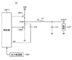
- FIG. 1 is a diagram showing a configuration of a switching power supply device according to the first embodiment.
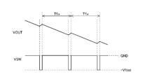
- FIG. 2 is a time chart showing the operation of the switching power supply device according to the first embodiment.
- FIG. 3 is a diagram showing a configuration of a switching power supply device according to a second embodiment.
- FIG. 4 is a time chart showing the operation of the switching power supply device according to the second embodiment.
- FIG. 5 is a diagram showing a configuration of a switching power supply device according to a third embodiment.
- FIG. 6 is a time chart showing the operation of the switching power supply device according to the third embodiment.
- FIG. 7 is a diagram showing a configuration of a switching power supply device according to a fourth embodiment.
- FIG. 8 is a time chart showing the operation of the switching power supply device according to the fourth embodiment.
- FIG. 9 is a diagram showing a configuration example of the switching power supply device according to the fifth embodiment.
- FIG. 10 is a time chart showing an operation example of the switching power supply device according to the fifth embodiment when an overshoot of the output voltage occurs.
- FIG. 11 is a diagram showing a state in which the inductor current is regenerated.
- FIG. 12 is a time chart of the load current.
- FIG. 13 is a time chart showing another operation example of the switching power supply device according to the fifth embodiment when an overshoot of the output voltage occurs.
- FIG. 14 is a diagram showing a state in which the inductor current is regenerated.
- FIG. 15 is a diagram showing a state in which the inductor current flows from the ground to the inductor through the body diode of the second switch.
- FIG. 16 is a waveform diagram of the inductor current and the switch voltage.
- FIG. 17 is a diagram showing a state in which the inductor current is regenerated.
- FIG. 18 is a diagram showing a state in which the inductor current flows from the inductor to the application end of the input voltage via the body diode of the first switch.
- FIG. 19 is a waveform diagram of the inductor current and the switch voltage.
- FIG. 20 is an external view showing an example of a vehicle configuration.
- a MOS transistor is a semiconductor whose gate structure is "a layer made of a semiconductor such as a conductor or a semiconductor having a small resistance value", an “insulating layer”, and a "P-type, N-type, or intrinsic semiconductor".
- FIG. 1 is a diagram showing a configuration of a switching power supply device according to the first embodiment.
- the switching power supply device 1A (hereinafter referred to as “switching power supply device 1A”) according to the first embodiment is a switching power supply device that steps down the input voltage VIN to the output voltage VOUT, and includes a control unit CNT1 and a first switch SW1.
- a second switch SW2, an inductor L1, an output capacitor C1, and an output feedback unit FB1 are provided.
- the switching power supply device 1A may be configured to operate in the current continuous mode when the load is light, or may have a backflow prevention function and operate in the current discontinuous mode when the load is light.
- the control unit CNT1 controls on / off of the first switch SW1 and the second switch SW2 based on the output of the output feedback unit FB1.
- the control unit CNT1 is a switch control device that controls on / off of the first switch SW1 and the second switch SW2.
- the first switch SW1 is configured so that the first end can be connected to the application end of the input voltage VIN and the second end can be connected to the first end of the inductor L1.
- the first switch SW1 conducts / cuts off the current path from the application end of the input voltage VIN to the inductor L1.
- a P-channel type MOS transistor, an N-channel type MOS transistor, or the like can be used as the first switch SW1 for example.
- a bootstrap circuit or the like may be provided in the switching power supply device 1A in order to generate a voltage larger than the input voltage VIN.
- the second switch SW2 is configured so that the first end can be connected to the first end of the inductor L1 and the second end of the first switch SW1 and the second end can be connected to the application end of the ground potential.
- the second switch SW2 conducts / cuts off the current path from the application end of the ground potential to the inductor L1.
- an N-channel type MOS transistor or the like can be used as the second switch SW2 for example.
- a pulsed switch voltage VSW is generated at the connection node of the first switch SW1 and the second switch SW2.
- the inductor L1 and the output capacitor C1 smooth the pulsed switch voltage VSW to generate an output voltage VOUT, and supply the output voltage VOUT to the application end of the output voltage VOUT.
- a load LD1 is connected to the application end of the output voltage VOUT, and the output voltage VOUT is supplied to the load LD1.
- the output feedback unit FB1 generates and outputs a feedback signal according to the output voltage VOUT.
- the output feedback unit FB1 for example, a resistance voltage divider circuit that generates a feedback signal by resistance dividing the output voltage VOUT can be used. Further, for example, the output feedback unit FB1 may be configured to acquire the output voltage VOUT and output the output voltage VOUT itself as a feedback signal.
- the output feedback unit FB1 is configured to generate and output a feedback signal according to the current flowing through the inductor L1 (hereinafter referred to as “inductor current IL”) in addition to the feedback signal corresponding to the output voltage VOUT. May be good.
- the output feedback unit FB1 also generates a feedback signal according to the inductor current IL, so that the current mode can be controlled.
- FIG. 2 is a time chart showing the operation of the switching power supply device 1A.
- the control unit CNT1 sets the length of the first state ST1 according to the feedback signal output from the output feedback unit FB1.
- the control unit CNT1 turns the first switch SW1 into an on state and turns the second switch SW2 into an off state.
- the switch voltage VSW becomes a value obtained by adding the forward voltage of the body diode of the first switch SW1 to the input voltage VIN, and then becomes substantially the same value as the input voltage VIN.
- the inductor current IL increases with the passage of time.
- control unit CNT1 switches the control state from the first state ST1 to the second state ST2.
- the control unit CNT1 turns the first switch SW1 into an off state and turns the second switch SW2 into an on state.
- the switch voltage VSW has substantially the same value as the ground potential GND.
- the inductor current IL decreases with the passage of time.
- the control unit CNT1 ends the second state ST2 and switches the control state from the second state ST2 to the third state ST3.
- a determination unit (not shown) for determining whether or not the inductor current IL has decreased to a predetermined value may be provided separately from the control unit CNT1 or may be built in the control unit CNT1. In this embodiment, the above predetermined value is set to zero.
- the control unit CNT1 turns off the first switch SW1 and the second switch SW2.
- the connection node of the first switch SW1 and the second switch SW2 is in the high impedance state, and the switch voltage VSW has substantially the same value as the output voltage VOUT.
- the inductor current IL becomes zero.
- the periodic signal S1 is a signal in which a pulse is generated with a fixed period Tfix.
- the periodic signal S1 may be a signal generated inside the control unit CNT1 or a signal generated outside the control unit CNT1 and acquired by the control unit CNT1.
- control unit CNT1 ends the third state ST3 and switches the control state from the third state ST3 to the fourth state ST4.
- the control unit CNT1 turns the first switch SW1 into an off state and turns the second switch SW2 into an on state.
- the switch voltage VSW has substantially the same value as the ground potential GND.
- the inductor current IL flows from the application end of the output voltage VOUT toward the connection node of the first switch SW1 and the second switch SW2, and the amount of current increases with the passage of time.
- the inductor current IL is regenerated. Since the regenerative energy of the inductor current IL is released when the fourth state ST4 is switched to the first state ST1, the switch voltage VSW rises sharply when the fourth state ST4 is switched to the first state ST1.
- control unit CNT1 ends the fourth state ST4 and switches the control state from the fourth state ST4 to the first state ST1.
- the control unit CNT1 repeats the first state ST1, the second state ST2, the third state ST3, and the fourth state ST4 in the fixed cycle Tfix.
- a dead time period during which both the first switch SW1 and the second switch SW2 are in the off state is set between the first state ST1 and the second state ST2, and between the fourth state ST4 and the first state ST1, respectively. It is desirable to provide it.
- the fixed period Tfix is the first state ST1, the first state ST1 and the first state.
- the dead time period provided between the two states ST2, the second state ST2, the third state ST3, the fourth state ST4, and the dead time period provided between the fourth state ST4 and the first state ST1 are totaled. Matches the period.
- the switching power supply device 1A Since the switching power supply device 1A operates in a fixed cycle Tfix and does not cause a loss in the third state ST3, high efficiency can be achieved without changing the switching frequency. Since the length of the first state ST1 becomes shorter and the length of the third state ST3 becomes longer when the load LD1 is a light load, the switching power supply unit 1A greatly improves the efficiency when the load LD1 is a light load. Can be made to.
- the second switch SW2 may be configured so that the second end can be connected to an application end having a lower voltage than the input voltage VIN and a low voltage other than the ground potential.
- FIG. 3 is a diagram showing a configuration of a switching power supply device according to a second embodiment.
- the switching power supply device 1B (hereinafter referred to as “switching power supply device 1B”) according to the second embodiment has a configuration in which a switch SW3 is added to the switching power supply device 1A.
- Switch SW3 is connected in parallel to switch SW2. That is, the first end of the switch SW3 is connected to the first end of the switch SW2, and the second end of the switch SW3 is connected to the second end of the switch SW2.
- the third switch SW3 for example, an N-channel type MOS transistor or the like can be used.
- the control unit CNT1 controls on / off of the third switch SW3 in addition to the on / off of the first switch SW1 and the second switch SW2.
- the switch SW3 has a smaller on-resistance (resistance between the first end and the second end in the on state) and a capacitance (parasitic capacitance between the first end and the second end) than the switch SW2. ..
- FIG. 4 is a time chart showing the operation of the switching power supply device 1B.
- the operation of the switching power supply device 1B is different from the operation of the switching power supply device 1A in that the control unit CNT1 turns off the second switch SW2 in the fourth state ST4.
- the control unit CNT1 turns on the third switch SW3 instead of the second switch SW2.
- the switching power supply unit 1B can make the loss in the fourth state ST4 smaller than that of the switching power supply unit 1A.
- the control unit CNT1 turns off the third switch SW3.
- the switching power supply device 1B Since the switching power supply device 1B operates in a fixed cycle Tfix and does not cause a loss in the third state ST3, high efficiency can be achieved without changing the switching frequency. Since the length of the first state ST1 becomes shorter and the length of the third state ST3 becomes longer when the load LD1 is a light load, the switching power supply unit 1B greatly improves the efficiency when the load LD1 is a light load. Can be made to.
- control unit CNT1 may turn on both the second switch SW2 and the third switch SW3.
- the second end of the second switch SW2 and the second end of the third switch SW3 are configured to be connectable to an application end having a voltage lower than the input voltage VIN and a low voltage other than the ground potential. You may.
- FIG. 5 is a diagram showing a configuration of a switching power supply device according to a third embodiment.
- the switching power supply device 1C (hereinafter referred to as “switching power supply device 1C”) according to the third embodiment has a configuration in which a switch SW3, a capacitance C2, and a switch SW4 are added to the switching power supply device 1A.
- the first end of the switch SW3 is connected to the connection node of the first switch SW1 and the second switch SW2.
- the second end of the switch SW3 is connected to the first end of the capacitance C2 and the first end of the fourth switch SW4.
- the second end of the capacitance C2 and the second end of the fourth switch SW4 are connected to the ground potential.
- As the third switch SW3, for example, an N-channel type MOS transistor or the like can be used.
- the fourth switch SW4 for example, an N-channel type MOS transistor or the like can be used.
- the control unit CNT1 controls on / off of the third switch SW3 and the fourth switch SW4 in addition to the on / off of the first switch SW1 and the second switch SW2.
- the switch SW3 has a smaller on-resistance (resistance between the first end and the second end in the on state) and a capacitance (parasitic capacitance between the first end and the second end) than the switch SW2. ..
- the switch SW3 may have the same on-resistance and capacitance as the switch SW2.
- the switch SW4 is a switch for discharging the capacitance C2. When the switch SW4 is turned on, both ends of the capacitance C2 are short-circuited and the capacitance C2 is discharged.
- FIG. 6 is a time chart showing the operation of the switching power supply device 1C.
- the operation of the switching power supply device 1C is basically the same as the operation of the switching power supply device 1B.
- on / off control of the fourth switch SW4 by the control unit CNT1 is added.
- the control unit CNT1 complementarily controls the on / off of the third switch SW3 and the on / off of the fourth switch SW4. That is, the control unit CNT1 turns on the fourth switch SW4 in the first state ST1, the second state ST2, and the third state ST3, and turns the fourth switch SW4 in the fourth state ST4.
- the switch voltage SW sets the input voltage VIN, the parasitic capacitance between the first end and the second end of the first switch SW1, and the first end of the third switch SW3.
- the voltage is divided by the parasitic capacitance and the capacitance C2 between the and the second end.
- the value of the switch voltage SW in the fourth state ST4 can be adjusted by the capacitance value of the capacitance C2. That is, the rising condition of the switch voltage VSW when switching from the fourth state ST4 to the first state ST1 can be adjusted by the capacitance value of the capacitance C2.
- control unit CNT1 in the semiconductor integrated circuit device and using the capacitance C2 as an external component of the semiconductor integrated circuit device, it becomes easy to adjust the value of the switch voltage SW in the fourth state ST4.
- the switching power supply device 1C Since the switching power supply device 1C operates in a fixed cycle Tfix and does not cause a loss in the third state ST3, high efficiency can be achieved without changing the switching frequency. Since the length of the first state ST1 becomes shorter and the length of the third state ST3 becomes longer when the load LD1 is a light load, the switching power supply unit 1C greatly improves the efficiency when the load LD1 is a light load. Can be made to.
- the second end of the second switch SW2, the second end of the capacitance C2, and the second end of the fourth switch SW4 are lower than the input voltage VIN and have a low voltage other than the ground potential. It may be configured to be connectable to the application end.
- FIG. 7 is a diagram showing a configuration of a switching power supply device according to a fourth embodiment.
- FIG. 8 is a time chart showing the operation of the switching power supply device according to the fourth embodiment.
- the switching power supply device 1D (hereinafter referred to as “switching power supply device 1D”) according to the fourth embodiment has a configuration in which a capacitance C2 is added to the switching power supply device 1A.
- the first end of the capacity C2 is connected to the connection node of the first switch SW1 and the second switch SW2.
- the control unit CNT1 controls the voltage VA applied to the second end of the switch SW3.
- the control unit CNT1 sets the voltage VA to the HIGH level (for example, the same value as the output voltage VOUT) in the third state ST3, and sets the voltage VA to the LOW level in the first state ST1, the second state ST2, and the fourth state ST4 (for example, the same value as the output voltage VOUT).
- the ground potential GND For example, the ground potential GND.
- the switching power supply device 1D Since the switching power supply device 1D operates in a fixed cycle Tfix and does not cause a loss in the third state ST3, high efficiency can be achieved without changing the switching frequency. Since the length of the first state ST1 becomes shorter and the length of the third state ST3 becomes longer when the load LD1 is a light load, the switching power supply unit 1D greatly improves the efficiency when the load LD1 is a light load. Can be made to.
- the second end of the second switch SW2 may be configured to be connectable to an application end having a voltage lower than the input voltage VIN and a low voltage other than the ground potential.
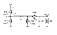
- FIG. 9 is a diagram showing a configuration example of the switching power supply device according to the fifth embodiment. It is a figure which shows the configuration example of a switching power supply device.
- the switching power supply device 1E (hereinafter referred to as “switching power supply device 1E”) according to the fifth embodiment of the configuration example shown in FIG. 9 is a switching power supply device that steps down the input voltage VIN to the output voltage VOUT, and is a control unit CNT1. , 1st to 4th switches SW1 to SW4, an inductor L1, an output capacitor C1, an output feedback unit FB1, and a detection unit DET1.
- the switching power supply device 1E may be configured to operate in the current continuous mode when the load is light, or may have a backflow prevention function and operate in the current discontinuous mode when the load is light.
- the control unit CNT1 controls on / off of the first to fourth switches SW1 to SW4 based on the outputs of the output feedback unit FB1 and the detection unit DET1.
- the control unit CNT1 is a switch control device that controls on / off of the first to fourth switches SW1 to SW4.
- the control unit CNT1 has an acquisition unit 2 that acquires the detection result of the detection unit DET1, and a first switch SW1, a second switch SW2, a third switch SW3, and a control unit SW3 based on the detection result of the detection unit DET1 acquired by the acquisition unit 2.
- the suppression unit 3 for suppressing the overshoot of the output voltage VOUT by turning on the switch SW3 is provided.
- the acquisition unit 2 and the suppression unit 3 may be realized by software, may be realized by a hardware circuit, or may be realized by the cooperation between the hardware and the hardware.
- the first switch SW1 is configured so that the first end can be connected to the application end of the input voltage VIN and the second end can be connected to the first end of the inductor L1.
- the first switch SW1 conducts / cuts off the current path from the application end of the input voltage VIN to the inductor L1.
- a P-channel type MOS transistor, an N-channel type MOS transistor, or the like can be used as the first switch SW1 .
- a bootstrap circuit or the like may be provided in the switching power supply device 1E in order to generate a voltage larger than the input voltage VIN.
- the second switch SW2 is configured so that the first end can be connected to the first end of the inductor L1 and the second end of the first switch SW1 and the second end can be connected to the application end of the ground potential.
- the second switch SW2 conducts / cuts off the current path from the application end of the ground potential to the inductor L1.
- the second switch SW2 may be configured so that the second end is lower than the input voltage VIN and can be connected to the application end of a voltage other than the ground potential.
- the voltage applied to the second end of the second switch SW2 is the same as the voltage applied to the second end of the third switch SW3.
- the second switch SW2 for example, an N-channel type MOS transistor or the like can be used.
- a pulsed switch voltage VSW is generated at the connection node of the first switch SW1 and the second switch SW2.
- the inductor L1 and the output capacitor C1 smooth the pulsed switch voltage VSW to generate an output voltage VOUT, and supply the output voltage VOUT to the application end of the output voltage VOUT.
- a load LD1 is connected to the application end of the output voltage VOUT, and the output voltage VOUT is supplied to the load LD1.
- the third switch SW3 is configured so that the first end can be connected to the second end of the inductor L1 and the second end can be connected to the application end of the ground potential.
- the third switch SW3 for example, an N-channel type MOS transistor or the like can be used.
- the fourth switch SW4 is configured so that the first end can be connected to the second end of the inductor L1 and the first end of the third switch, and the second end can be connected to the application end of the output voltage VOUT.
- the fourth switch SW4 for example, an N-channel type MOS transistor or the like can be used.
- the withstand voltage of the third switch SW3 and the fourth switch SW4 may be lower than the withstand voltage of the first switch SW1 and the second switch SW2. Therefore, the size of the third switch SW3 and the fourth switch SW4 can be reduced. Further, by making the third switch SW3 and the fourth switch SW4 smaller, the loss generated in each parasitic capacitance of the third switch SW3 and the fourth switch SW4 can be reduced.
- the output feedback unit FB1 generates and outputs a feedback signal according to the output voltage VOUT.
- the output feedback unit FB1 for example, a resistance voltage divider circuit that generates a feedback signal by resistance dividing the output voltage VOUT can be used. Further, for example, the output feedback unit FB1 may be configured to acquire the output voltage VOUT and output the output voltage VOUT itself as a feedback signal.
- the output feedback unit FB1 is configured to generate and output a feedback signal according to the current flowing through the inductor L1 (hereinafter referred to as “inductor current IL”) in addition to the feedback signal corresponding to the output voltage VOUT. May be good.
- the output feedback unit FB1 also generates a feedback signal according to the inductor current IL, so that the current mode can be controlled.
- the detection unit DET1 detects the occurrence and convergence of an overshoot of the output voltage VOUT.
- a comparator that inputs the output voltage VOUT to the non-inverting input terminal and inputs a constant voltage (a voltage larger than the target value of the output voltage VOUT) to the inverting input terminal can be used.
- the comparator switches the output signal from low level to high level when an overshoot of the output voltage VOUT occurs.
- the comparator switches the output signal from high level to low level when the overshoot of the output voltage VOUT converges.
- FIG. 10, which will be described later, illustrates this exemplary output signal.
- the divided voltage of the output voltage VOUT may be input to the non-inverting input terminal of the comparator instead of the output voltage VOUT, and the divided voltage of the constant voltage may be input to the inverting input terminal of the comparator instead of the constant voltage.
- the value of the output voltage VOUT at the time of detecting the occurrence of overshoot and the overshoot convergence detection are detected.
- the value of the output voltage VOUT at the time point can be different from each other.
- the detection unit DET1 does not necessarily have to detect the convergence of the overshoot of the output voltage VOUT. For example, when a counter is provided in the control unit CNT1 and a certain period of time measured by the counter elapses from the time when the detection unit DET1 detects the occurrence of an overshoot of the output voltage VOUT, the control unit CNT1 causes the overshoot of the output voltage VOUT to occur. It may be determined that it has converged.
- the detection unit DET1 detects a sign of an overshoot of the output voltage VOUT and the detection unit DET1 detects a sign of an overshoot of the output voltage VOUT
- the above-mentioned suppression The unit 3 may turn off the first switch SW1 and the second switch SW2 and turn on the third switch SW3 to suppress the overshoot of the output voltage VOUT.
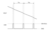
- FIG. 10 is a time chart showing an operation example of the switching power supply device 1E when an overshoot of the output voltage VOUT occurs.
- the switching power supply device 1E When the occurrence of overshoot of the output voltage VOUT is detected by the detection unit DET1, the switching power supply device 1E becomes the second state START2 under the control of the control unit CNT1.
- the occurrence of an overshoot of the output voltage VOUT is detected by the detection unit DET1 in the middle of the first state START1 (in the middle of the on-duty period of the switch SW), and the output of the detection unit DET1 changes from low level to high level.
- the first switch SW1 and the fourth switch SW4 In the first state START1, the first switch SW1 and the fourth switch SW4 are in the on state, and the second switch SW2 and the third switch SW3 are in the off state under the control of the control unit CNT1.
- the first switch SW1 and the fourth switch SW4 are turned off, and the second switch SW2 and the third switch SW3 are turned on under the control of the control unit CNT1.
- the inductor current IL is closed including the second switch SW2, the inductor L1 and the third switch SW3 as shown in FIG. Regenerate in the circuit.
- the current supply to the load LD1 side can be cut off.
- the fourth switch SW4 since the fourth switch SW4 is in the off state, the output voltage VOUT can be substantially clamped near the level at the time of overshoot occurrence.
- the output voltage VOUT is further increased by turning off the first switch SW1 and the fourth switch SW4 and turning on the second switch SW2 and the third switch SW3 when the overshoot of the output voltage VOUT occurs. It can be prevented and overshoot of the output voltage VOUT can be suppressed.
- the state of the switching power supply device 1E is maintained in the second state START2 until the convergence of the overshoot of the output voltage VOUT is detected by the detection unit DET1. While the second state START2 is maintained, the inductor current IL gradually decreases due to the on-resistance of the second switch SW2 and the on-resistance of the third switch SW3.
- the state of the switching power supply device 1E is changed from the second state STATE2 to the first state.
- the transition to START1 is made, but this transition is merely an example. That is, after the end of the second state START2, the state may be changed to a state other than the first state START1.
- the second state START2 is maintained without being interrupted from the occurrence of the overshoot of the output voltage VOUT to the convergence.
- the second state START 2 may be temporarily interrupted between the occurrence of the overshoot of the output voltage VOUT and the convergence. The second state START 2 may be terminated without waiting for the overshoot of the output voltage VOUT to converge.
- FIG. 13 is a time chart showing other operations of the switching power supply device 1E when an overshoot of the output voltage VOUT occurs.
- the switching power supply device 1E When the occurrence of overshoot of the output voltage VOUT is detected by the detection unit DET1, the switching power supply device 1E becomes the second state START2 under the control of the control unit CNT1.
- the occurrence of an overshoot of the output voltage VOUT is detected by the detection unit DET1 in the middle of the first state START1 (during the on-duty period of the switch voltage VSW), and the output of the detection unit DET1 is from low level to high level. It is a time chart when the state of the switching power supply device 1E changes from the first state START1 to the second state START2.
- the first switch SW1 and the second switch SW2 complementarily switch between the on state and the off state with the fixed cycle Tfix based on the periodic signal S1 under the control of the control unit CNT1, and the third switch SW3 is turned off.
- the state is set, and the fourth switch SW4 is in the ON state.
- the periodic signal S1 is a signal in which a pulse is generated with a fixed period Tfix.
- the periodic signal S1 may be a signal generated inside the control unit CNT1 or a signal generated outside the control unit CNT1 and acquired by the control unit CNT1. It is desirable to provide a dead time period in which both the first switch SW1 and the second switch SW2 are in the off state when the first switch SW1 and the second switch SW2 are complementarily switched between the on state and the off state.
- the first switch SW1 is turned off by the control of the control unit CNT1, and the on state and the off state of the second to fourth switches SW2 to SW4 are switched in the fixed cycle Tfix.
- the second switch SW2, the third switch SW3, and the fourth switch SW4 complementarily switch between the on state and the off state with a fixed cycle Tfix.
- the control unit CNT1 switches between the on state and the off state of the second to fourth switches SW2 to SW4 based on the periodic signal S1.
- the state START 2-1 is a period in which the second switch SW2 and the third switch SW3 are in the on state and the fourth switch SW4 is in the off state
- the state START 2-2 is a state in which the second switch SW2 and the third switch SW3 are in the off state. This is the period during which the fourth switch SW4 is in the ON state.
- the state of the switching power supply device 1E is maintained in the second state START2 until the convergence of the overshoot of the output voltage VOUT is detected by the detection unit DET1. While the second state START2 is maintained, the inductor current IL gradually decreases due to the on-resistance of the second switch SW2 and the on-resistance of the third switch SW3.
- the state of the switching power supply device 1E is changed from the second state STATE2 to the third state. Transition to START3.
- the first to third switches SW1 to SW3 are turned off and the fourth switch SW4 is turned on by the control of the control unit CNT1.
- the details of the state STATE2-1 and the state START2-2 will be described by taking as an example the case where the N-channel type MOS transistor is used for the first to fourth switches SW1 to SW4.
- bipolar transistors may be used for the first to fourth switches SW1 to SW4, and a "reverse connection diode" may be connected in parallel to each bipolar transistor.
- the direction in which the current of the "reverse connection diode” flows is opposite to the direction in which the current of the bipolar transistor connected in parallel to the "reverse connection diode" flows.
- the inductor current IL is closed including the second switch SW2, the inductor L1, and the third switch SW3. It regenerates in the circuit, and the switch voltage SW and the ground potential become substantially the same.
- the fourth switch SW4 since the fourth switch SW4 is in the off state, the current supply to the load LD1 side can be cut off. Therefore, the output voltage VOUT can be substantially clamped to the vicinity of the level at the time of overshoot occurrence. That is, the output voltage VOUT is further increased by turning off the first switch SW1 and the fourth switch SW4 and turning on the second switch SW2 and the third switch SW3 when the overshoot of the output voltage VOUT occurs. It can be prevented and overshoot of the output voltage VOUT can be suppressed.
- the period of each state START2-2 is a fixed period. Specifically, the period of each state STATE2-2 is a fixed period corresponding to the pulse width of the periodic signal S1. It is desirable that the period of each state STATE2-2 is 1/10 or less of the fixed period Tfix. This is because when the period of each state START2-2 is longer than 1/10 of the fixed period Tfix, the time required for the overshoot of the output voltage VOUT to converge exceeds the allowable range.
- the output voltage VOUT and the switch voltage VSW in the second state START are as shown in FIG. It should be noted that the output voltage VOUT is enlarged with respect to the switch voltage VSW with respect to the scale in the vertical direction of the paper surface of FIG.
- the cycle of the switch voltage VSW is a fixed cycle Tfix. That is, since the frequency (switching frequency) of the switch voltage VSW does not fluctuate, the frequency of noise caused by the switching frequency also does not fluctuate. Therefore, there is no possibility that the effect of the noise suppressing means (for example, a filter circuit) for suppressing the noise of a fixed frequency is reduced.
- the inductor current IL is closed including the second switch SW2, the inductor L1, and the third switch SW3. It regenerates in the circuit, and the switch voltage SW and the ground potential become substantially the same.
- the fourth switch SW4 since the fourth switch SW4 is in the off state, the current supply to the load LD1 side can be cut off. Therefore, the output voltage VOUT can be substantially clamped to the vicinity of the level at the time of overshoot occurrence. That is, the output voltage VOUT is further increased by turning off the first switch SW1 and the fourth switch SW4 and turning on the second switch SW2 and the third switch SW3 when the overshoot of the output voltage VOUT occurs. It can be prevented and overshoot of the output voltage VOUT can be suppressed.
- the inductor current IL is from the inductor L1 to the input voltage VIN via the body diode of the first switch SW1. It flows toward the application end. Therefore, the switch voltage VSW becomes VIN + Vf SW1 . Note that Vf SW1 is the forward voltage of the body diode of the first switch SW1.
- the output voltage VOUT and the switch voltage VSW in the second state START are as shown in FIG. It should be noted that the output voltage VOUT is enlarged with respect to the switch voltage VSW with respect to the scale in the vertical direction of the paper in FIG. As can be seen from FIG. 19, the cycle of the switch voltage VSW is a fixed cycle Tfix. That is, since the frequency (switching frequency) of the switch voltage VSW does not fluctuate, the frequency of noise caused by the switching frequency also does not fluctuate. Therefore, there is no possibility that the effect of the noise suppressing means (for example, a filter circuit) for suppressing the noise of a fixed frequency is reduced.
- the noise suppressing means for example, a filter circuit
- control unit CNT1 may turn on the second switch SW2 in the state START2-2. Further, when the inductor current IL is in the negative direction, unlike this operation example, the control unit CNT1 may turn on the first switch SW1 in the state START2-2.
- the set value of the fixed cycle Tfix may be changeable. By changing the cycle of the cycle signal S1, the set value of the fixed cycle Tfix can be changed.
- FIG. 9 is an external view showing a configuration example of a vehicle equipped with an in-vehicle device.
- the vehicle X of this configuration example is equipped with in-vehicle devices X11 to X17 and a battery (not shown) for supplying electric power to these in-vehicle devices X11 to X17.
- the control unit CNT1 When any of the switching power supply devices 1A to 1E described above is mounted on the vehicle X, it is required to suppress the radiation noise in the AM band so that the reception of the AM radio broadcast is not adversely affected. Therefore, it is desirable that the control unit CNT1 generate a voltage of 1.8 MHz or more and 2.1 MHz or less at the connection node of the first switch SW1 and the second switch SW2. That is, it is desirable that the control unit CNT1 sets the frequency (switching frequency) of the switch voltage VSW to 1.8 MHz or more and 2.1 MHz or less. This is because when the switching frequency is less than 1.8 MHz, the radiation noise in the AM band increases, and when the switching frequency is larger than 2.1 MHz, the switching loss exceeds the allowable range.
- the in-vehicle device X11 is an engine control unit that performs control related to the engine (injection control, electronic throttle control, idling control, oxygen sensor heater control, auto cruise control, etc.).
- the in-vehicle device X12 is a lamp control unit that controls turning on and off such as HID [high intensity discharged lamp] and DRL [daytime running lamp].
- the in-vehicle device X13 is a transmission control unit that performs control related to the transmission.
- the in-vehicle device X14 is a body control unit that performs control related to the movement of the vehicle X (ABS [anti-lock brake system] control, EPS [electric power steering] control, electronic suspension control, etc.).
- ABS anti-lock brake system
- EPS electric power steering
- electronic suspension control etc.
- the in-vehicle device X15 is a security control unit that controls the drive of door locks, security alarms, and the like.
- the in-vehicle device X16 is an electronic device incorporated in the vehicle X at the factory shipment stage as a standard equipment or a manufacturer's option such as a wiper, an electric door mirror, a power window, an electric sunroof, an electric seat, and an air conditioner.
- the in-vehicle device X17 is an electronic device that is arbitrarily attached to the vehicle X by the user, such as an in-vehicle A / V [audio / visual] device, a car navigation system, and an ETC [Electronic Toll Collection System].
- the switching power supply devices 1A to 1E described above can be incorporated into any of the in-vehicle devices X11 to X17, respectively.
- the set value of the fixed cycle Tfix may be changeable. By changing the cycle of the cycle signal S1, the set value of the fixed cycle Tfix can be changed.
- the integrated circuit package incorporating the first switch SW1 and the second switch SW2 and the integrated circuit package since the third switch SW4 and the fourth switch SW4 have a lower withstand voltage than the first switch SW1 and the second switch SW2, the integrated circuit package incorporating the first switch SW1 and the second switch SW2 and the integrated circuit package. It is preferable to make the integrated circuit package containing the third switch SW3 and the fourth switch SW4 into separate integrated circuit packages. As a result, each integrated circuit package can be efficiently designed and manufactured.
- first to fourth switches SW1 to SW4 may be built in the same integrated circuit package. Further, the first to fourth switches SW1 to SW4 may be discrete parts.
- the switching power supply device is a switching power supply device configured to step down the input voltage to the output voltage, and the first end is configured to be connectable to the application end of the input voltage.
- the first switch is configured so that the second end can be connected to the first end of the inductor, and the first end is configured to be connectable to the first end of the inductor and the second end of the first switch.
- a second switch configured to be connectable to an application end having a voltage lower than the input voltage, and a control unit configured to control the on / off of the first switch and the second switch.
- the control unit turns the first switch on and turns the second switch off, and after the first state, turns the first switch off and turns the second switch on.
- the switching power supply device having the first configuration described above can improve efficiency without changing the switching frequency.
- control unit may have a configuration (second configuration) in which the first switch is turned off and the second switch is turned on in the fourth state.
- the switching power supply device having the second configuration can regenerate the current flowing through the inductor in the fourth state.
- the control unit includes a third switch which is configured to be connectable to the second switch in parallel and has at least one of the on-resistance and the capacitance smaller than that of the second switch. Is configured to control the on / off of the third switch, and the control unit has a configuration in which the first switch is turned off and the third switch is turned on in the fourth state (third state). Configuration) may be used.
- the switching power supply device having the third configuration can reduce the loss in the fourth state.
- the first end is a third switch configured to be connectable to the first end of the inductor and the second end of the first switch, and the first end is the third switch.
- the control unit is configured to control on / off of the third switch.
- the control unit may be configured to turn off the first switch and turn on the third switch in the fourth state (fourth configuration).
- the rise of the switch voltage generated in the connection node of the first switch and the second switch when the fourth state is switched to the first state according to the capacitance value of the capacitance. Can be adjusted.
- the switching power supply device having the fourth configuration includes a fourth switch configured to be connectable in parallel to the capacitance, and the control unit is configured to control on / off of the fourth switch. May have a configuration (fifth configuration) in which the on / off of the third switch and the on / off of the fourth switch are controlled in a complementary manner.
- the switching power supply device having the fifth configuration described above can discharge the capacity at an appropriate timing.
- the first end is configured to be connectable to the first end of the inductor and the second end of the first switch, and the second end is connectable to the end to which a variable voltage is applied.
- the control unit is configured to control the variable voltage, and the control unit turns off the first switch in the fourth state and controls the variable voltage to control the capacity.
- a configuration (sixth configuration) may be used in which a potential difference is generated between the first end and the second end.
- the switching power supply device having the sixth configuration is generated at the connection node of the first switch and the second switch when the fourth state is switched to the first state by adjusting the value of the variable voltage in the fourth state.
- the rise of the switch voltage can be adjusted.
- the switching power supply device is a switching power supply device configured to step down the input voltage to the output voltage, and the first end is configured to be connectable to the application end of the input voltage.
- the first switch is configured so that the second end can be connected to the first end of the inductor, and the first end is configured to be connectable to the first end of the inductor and the second end of the first switch. Is configured to be connectable to the application end of a low voltage lower than the input voltage, and the first end is configured to be connectable to the second end of the inductor, and the second end is the application of the low voltage.
- a third switch that can be connected to the end, a first end that can be connected to the second end of the inductor and the first end of the third switch, and the second end to the application end of the output voltage.
- a fourth switch configured to be connectable, a detection unit configured to detect the occurrence or a sign of overshoot of the output voltage, the first switch, the second switch, the third switch, and the said.
- the control unit includes a control unit configured to control the on / off of the fourth switch, and when the detection unit detects the occurrence or a sign of overshoot of the output voltage, the first control unit.
- the configuration is such that the switch and the fourth switch are turned off, and the second switch and the third switch are turned on (seventh configuration).
- the switching power supply device having the seventh configuration can suppress overshoot of the output voltage.
- the detection unit also detects the convergence of the overshoot of the output voltage, and the control unit detects the convergence of the overshoot of the output voltage by the detection unit.
- the third switch may be turned off and the fourth switch may be turned on (eighth configuration).
- the switching power supply device having the eighth configuration can reliably suppress the overshoot of the output voltage until the overshoot of the output voltage converges.
- the detection unit in the control unit, after the detection unit detects the occurrence or a sign of the overshoot of the output voltage, the detection unit converges the overshoot of the output voltage.
- the first switch and the fourth switch are turned off, and the second switch is turned on and the third switch is used.
- a configuration (9th configuration) may be used in which the on state, the off state of the second switch, and the off state of the third switch are switched at a fixed cycle.
- the switching power supply device having the ninth configuration can suppress fluctuations in the noise frequency.
- the off state period of the second switch and the third switch may be a fixed period (tenth configuration).
- the switching power supply device having the tenth configuration can stably suppress output voltage overshoot every cycle.
- the off state period of the second switch and the third switch may be 1/10 or less of the fixed cycle (11th configuration).
- the switching power supply device having the eleventh configuration can prevent the time required for the overshoot of the output voltage to converge from exceeding the allowable range.
- the switching power supply device having the twelfth configuration can suppress radiation noise and switching loss in the AM band.
- the first switch is configured so that the first end can be connected to the application end of the input voltage and the second end can be connected to the first end of the inductor. On / off, the first end can be connected to the first end of the inductor and the second end of the first switch, and the second end can be connected to the application end of a low voltage lower than the input voltage.
- a switch control device that controls the on / off of the configured second switch, the first state in which the first switch is turned on and the second switch is turned off, and the first state.
- the third state After the third state, it has a fourth state in which the voltage of the connection node between the first switch and the second switch is lower than that in the third state, and the first state and the second state have a fixed cycle. It is a configuration (13th configuration) in which the state, the third state, and the fourth state are repeated.
- the switch control device having the thirteenth configuration can improve the efficiency of the switching power supply device equipped with the switch control device without changing the switching frequency of the switching power supply device equipped with the switch control device.
- the first switch is configured so that the first end can be connected to the application end of the input voltage and the second end can be connected to the first end of the inductor.
- the first end can be connected to the first end of the inductor and the second end of the first switch, and the second end can be connected to the application end of a low voltage lower than the input voltage.
- the third switch configured so that the first end can be connected to the second end of the inductor and the second end can be connected to the low voltage application end.
- a fourth switch configured so that the first end can be connected to the second end of the inductor and the first end of the third switch, and the second end can be connected to the applied end of the output voltage.
- a switch control device that controls the on / off of the output voltage, the acquisition unit configured to acquire the detection result of the detection unit that detects the occurrence or sign of overshoot of the output voltage, and the acquisition unit.
- the on / off of the first switch, the second switch, the third switch, and the fourth switch is controlled based on the acquired detection result, and the detection unit causes the overshoot of the output voltage or a sign thereof.
- the first switch and the fourth switch are turned off, and the second switch and the third switch are turned on to suppress the overshoot of the output voltage. (14th configuration).
- the switch control device having the above 14th configuration can suppress overshoot of the output voltage.
- the in-vehicle device described above has a configuration (15th configuration) including a switching power supply device having any one of the first to twelfth configurations or a switch control device having the thirteenth or fourteenth configuration.
- the vehicle-mounted device having the fifteenth configuration is intended to improve the efficiency of the switching power supply device mounted on the vehicle-mounted device without changing the switching frequency of the switching power supply device mounted on the vehicle-mounted device, or the vehicle-mounted device. It is possible to suppress overshoot of the output voltage of the switching power supply device mounted on the in-vehicle device.
- the vehicle described above has a configuration (sixteenth configuration) including an in-vehicle device having the fifteenth configuration and a battery for supplying electric power to the in-vehicle device.
- the efficiency of the switching power supply device mounted on the vehicle can be improved without changing the switching frequency of the switching power supply device mounted on the vehicle, or the in-vehicle device can be used. It is possible to suppress overshoot of the output voltage of the mounted switching power supply device.
- Switching power supply device 1A to 1E Switching power supply device according to the first to fifth embodiments 2 Acquisition unit 3 Suppression unit C1 Output capacitor C2 Capacity CNT1 Control unit DET1 Detection unit FB1 Output feedback unit L1 Inductor LD1 Load SW1 to SW4 1st to 4th switches X Vehicle X11-X17 In-vehicle equipment
Landscapes
- Engineering & Computer Science (AREA)
- Power Engineering (AREA)
- Dc-Dc Converters (AREA)
Abstract
This switching power supply device comprises: first and second switches that are connected in series between the applying terminal of an input voltage and the applying terminal of a voltage lower than the input voltage; and a control unit configured to control on/off of the first switch and the second switch. The control unit has: a first state in which the first switch is in an ON state and the second switch is in an OFF state; a second state in which the first switch is in the OFF state and the second switch is in the ON state after the first state; a third state in which the first switch and the second switch are in the OFF state after the second state; and a fourth state in which the voltage of a connection node between the first switch and the second switch is lowered compared to the third state after the third state. The control unit repeats, at a fixed period, the first state, the second state, the third state, and the fourth state.
Description
本明細書中に開示されている発明は、入力電圧を出力電圧に降圧するスイッチング電源装置、スイッチ制御装置、車載機器、及び車両に関する。
The invention disclosed in the present specification relates to a switching power supply device, a switch control device, an in-vehicle device, and a vehicle that step down an input voltage to an output voltage.
従来、軽負荷時の効率が高いスイッチング電源装置として、オン時間固定制御方式のスイッチング電源装置が知られている(例えば特許文献1参照)。
Conventionally, as a switching power supply device having high efficiency at the time of light load, a switching power supply device having a fixed on-time control method is known (see, for example, Patent Document 1).
また、入力電圧を出力電圧に降圧する降圧型スイッチング電源装置では、一般的に出力電流が急峻に減少すると、出力電圧にオーバーシュートが生じる。
Further, in a step-down switching power supply device that steps down the input voltage to the output voltage, generally, when the output current suddenly decreases, the output voltage overshoots.
オン時間固定制御方式のスイッチング電源装置は、負荷の状態に応じてスイッチング周波数が可変するという特徴を有する。スイッチング周波数が変動すると、ノイズの周波数も変動するので、固定周波数のノイズを抑制するノイズ抑制手段(例えばフィルタ回路など)の効果が減少してしまうことがある。したがって、ノイズが問題となる環境下で使用されるスイッチング電源装置のスイッチング周波数は固定であることが望ましい。
The on-time fixed control type switching power supply has the feature that the switching frequency changes according to the load condition. When the switching frequency fluctuates, the noise frequency also fluctuates, so that the effect of the noise suppressing means (for example, a filter circuit) for suppressing the noise of a fixed frequency may be reduced. Therefore, it is desirable that the switching frequency of the switching power supply used in an environment where noise is a problem is fixed.
出力コンデンサの静電容量を大きくすることで出力電圧のオーバーシュートを抑制することができる。しかしながら、出力コンデンサの静電容量を大きくすることは、装置の大型化及びコストアップの要因となる。このため、出力コンデンサの静電容量を大きくせずとも出力電圧のオーバーシュートを抑制できる手法が望まれている。
By increasing the capacitance of the output capacitor, overshoot of the output voltage can be suppressed. However, increasing the capacitance of the output capacitor causes an increase in the size and cost of the device. Therefore, a method capable of suppressing an overshoot of the output voltage without increasing the capacitance of the output capacitor is desired.
特許文献2に開示されているスイッチング電源装置では、インダクタに並列接続される短絡スイッチのオン状態とオフ状態とを繰り返すことによって、又は、インダクタに並列接続される短絡スイッチのオン抵抗を変化させることによって、出力電圧のアンダーシュート及びオーバーシュートを抑制している。
In the switching power supply device disclosed in Patent Document 2, the on-resistance of the short-circuit switch connected in parallel to the inductor is changed by repeating the on-state and the off-state of the short-circuit switch connected in parallel to the inductor. This suppresses the undershoot and overshoot of the output voltage.
しかしながら、特許文献2に開示されているスイッチング電源装置は、出力電圧のオーバーシュートを抑制する際に、短絡スイッチと整流スイッチの両方をオンにするので、負荷から短絡スイッチ及び整流スイッチを介してグランドに電流が流れ、損失が大きくなるという問題を有している。
However, the switching power supply device disclosed in Patent Document 2 turns on both the short-circuit switch and the rectification switch when suppressing the overshoot of the output voltage, so that the load is grounded via the short-circuit switch and the rectification switch. There is a problem that a current flows through the circuit and the loss becomes large.
また、特許文献2に開示されているスイッチング電源装置では、短絡スイッチをパワースイッチ及び整流スイッチと同程度の耐圧にする必要がある。そのため、例えば短絡スイッチをシリコンデバイスで実現する場合には、短絡スイッチが大型化してしまう。
Further, in the switching power supply device disclosed in Patent Document 2, it is necessary to make the short-circuit switch have a withstand voltage comparable to that of the power switch and the rectifying switch. Therefore, for example, when the short-circuit switch is realized by a silicon device, the short-circuit switch becomes large in size.
本明細書中に開示されている第1の局面に係るスイッチング電源装置は、入力電圧を出力電圧に降圧するよう構成されるスイッチング電源装置であって、第1端が前記入力電圧の印加端に接続可能に構成され、第2端がインダクタの第1端に接続可能に構成される第1スイッチと、第1端が前記インダクタの第1端及び前記第1スイッチの第2端に接続可能に構成され、第2端が前記入力電圧よりも低い低電圧の印加端に接続可能に構成される第2スイッチと、前記第1スイッチ及び前記第2スイッチのオン/オフを制御するよう構成される制御部と、を備え、前記制御部は、前記第1スイッチをオン状態にし、前記第2スイッチをオフ状態にする第1状態と、前記第1状態の後に前記第1スイッチをオフ状態にし、前記第2スイッチをオン状態にする第2状態と、前記第2状態の後に前記第1スイッチ及び前記第2スイッチをオフ状態にする第3状態と、前記第3状態の後に、前記第3状態よりも前記第1スイッチと前記第2スイッチとの接続ノードの電圧を低くする第4状態と、を有し、固定周期で前記第1状態、前記第2状態、前記第3状態、及び前記第4状態を繰り返す構成である。
The switching power supply device according to the first aspect disclosed in the present specification is a switching power supply device configured to step down the input voltage to the output voltage, and the first end is at the application end of the input voltage. A first switch configured to be connectable and having a second end connectable to the first end of the inductor, and a first end connectable to the first end of the inductor and the second end of the first switch. A second switch configured such that the second end can be connected to an application end having a voltage lower than the input voltage, and the first switch and the second switch being configured to control on / off. A control unit is provided, and the control unit sets a first state in which the first switch is turned on and the second switch is turned off, and a first state in which the first switch is turned off after the first state. A second state in which the second switch is turned on, a third state in which the first switch and the second switch are turned off after the second state, and a third state after the third state. It has a fourth state in which the voltage of the connection node between the first switch and the second switch is lowered, and the first state, the second state, the third state, and the first state in a fixed cycle. It is a configuration that repeats four states.
本明細書中に開示されている第2の局面に係るスイッチング電源装置は、入力電圧を出力電圧に降圧するよう構成されるスイッチング電源装置であって、第1端が前記入力電圧の印加端に接続可能に構成され、第2端がインダクタの第1端に接続可能に構成される第1スイッチと、第1端が前記インダクタの第1端及び前記第1スイッチの第2端に接続可能に構成され、第2端が前記入力電圧よりも低い低電圧の印加端に接続可能に構成される第2スイッチと、第1端が前記インダクタの第2端に接続可能に構成され、第2端が前記低電圧の印加端に接続可能に構成される第3スイッチと、第1端が前記インダクタの第2端及び前記第3スイッチの第1端に接続可能に構成され、第2端が前記出力電圧の印加端に接続可能に構成される第4スイッチと、前記出力電圧のオーバーシュートの発生又はその予兆を検出するよう構成される検出部と、前記第1スイッチ、前記第2スイッチ、前記第3スイッチ、及び前記第4スイッチのオン/オフを制御するよう構成される制御部と、を備え、前記制御部は、前記検出部によって前記出力電圧のオーバーシュートの発生又はその予兆が検出されると、前記第1スイッチ及び前記第4スイッチをオフ状態にし、前記第2スイッチ及び前記第3スイッチをオン状態にする構成である。
The switching power supply device according to the second aspect disclosed in the present specification is a switching power supply device configured to step down the input voltage to the output voltage, and the first end is at the application end of the input voltage. A first switch configured to be connectable and having a second end connectable to the first end of the inductor, and a first end connectable to the first end of the inductor and the second end of the first switch. The second switch is configured so that the second end can be connected to the application end of a voltage lower than the input voltage, and the first end can be connected to the second end of the inductor. Is configured to be connectable to the low voltage application end, the first end is configured to be connectable to the second end of the inductor and the first end of the third switch, and the second end is the said. A fourth switch that can be connected to the application end of the output voltage, a detection unit that is configured to detect the occurrence or a sign of overshoot of the output voltage, the first switch, the second switch, and the above. A third switch and a control unit configured to control the on / off of the fourth switch are provided, and the control unit detects the occurrence or a sign of overshoot of the output voltage by the detection unit. Then, the first switch and the fourth switch are turned off, and the second switch and the third switch are turned on.
本明細書中に開示されている第3の局面に係るスイッチ制御装置は、第1端が入力電圧の印加端に接続可能に構成され、第2端がインダクタの第1端に接続可能に構成される第1スイッチのオン/オフと、第1端が前記インダクタの第1端及び前記第1スイッチの第2端に接続可能に構成され、第2端が前記入力電圧よりも低い低電圧の印加端に接続可能に構成される第2スイッチのオン/オフと、を制御するスイッチ制御装置であって、前記第1スイッチをオン状態にし、前記第2スイッチをオフ状態にする第1状態と、前記第1状態の後に前記第1スイッチをオフ状態にし、前記第2スイッチをオン状態にする第2状態と、前記第2状態の後に前記第1スイッチ及び前記第2スイッチをオフ状態にする第3状態と、前記第3状態の後に、前記第3状態よりも前記第1スイッチと前記第2スイッチとの接続ノードの電圧を低くする第4状態と、を有し、固定周期で前記第1状態、前記第2状態、前記第3状態、及び前記第4状態を繰り返す構成である。
The switch control device according to the third aspect disclosed in the present specification is configured so that the first end can be connected to the application end of the input voltage and the second end can be connected to the first end of the inductor. The first switch is turned on / off, and the first end is configured to be connectable to the first end of the inductor and the second end of the first switch, and the second end has a low voltage lower than the input voltage. A switch control device that controls the on / off of a second switch that can be connected to the application end, and is a first state in which the first switch is turned on and the second switch is turned off. After the first state, the first switch is turned off and the second switch is turned on, and after the second state, the first switch and the second switch are turned off. It has a third state, and after the third state, a fourth state in which the voltage of the connection node between the first switch and the second switch is lower than that of the third state, and the first state has a fixed cycle. The configuration is such that one state, the second state, the third state, and the fourth state are repeated.
本明細書中に開示されている第4の局面に係るスイッチ制御装置は、第1端が入力電圧の印加端に接続可能に構成され、第2端がインダクタの第1端に接続可能に構成される第1スイッチのオン/オフと、第1端が前記インダクタの第1端及び前記第1スイッチの第2端に接続可能に構成され、第2端が前記入力電圧よりも低い低電圧の印加端に接続可能に構成される第2スイッチのオン/オフと、第1端が前記インダクタの第2端に接続可能に構成され、第2端が前記低電圧の印加端に接続可能に構成される第3スイッチのオン/オフと、第1端が前記インダクタの第2端及び前記第3スイッチの第1端に接続可能に構成され、第2端が出力電圧の印加端に接続可能に構成される第4スイッチのオン/オフと、を制御するスイッチ制御装置であって、前記出力電圧のオーバーシュートの発生又はその予兆を検出する検出部の検出結果を取得するよう構成される取得部と、前記取得部によって取得された前記検出結果に基づき前記第1スイッチ、前記第2スイッチ、第3スイッチ、及び前記第4スイッチのオン/オフを制御し、前記検出部によって前記出力電圧のオーバーシュートの発生又はその予兆が検出されると、前記第1スイッチ及び前記第4スイッチをオフ状態にし、前記第2スイッチ及び第3スイッチをオン状態にして前記出力電圧のオーバーシュートを抑制するよう構成される抑制部と、を備える構成である。
The switch control device according to the fourth aspect disclosed in the present specification is configured so that the first end can be connected to the application end of the input voltage and the second end can be connected to the first end of the inductor. The first switch is turned on / off, and the first end is configured to be connectable to the first end of the inductor and the second end of the first switch, and the second end has a low voltage lower than the input voltage. The on / off of the second switch configured to be connectable to the application end, the first end configured to be connectable to the second end of the inductor, and the second end configured to be connectable to the low voltage application end. The on / off of the third switch and the first end can be connected to the second end of the inductor and the first end of the third switch, and the second end can be connected to the application end of the output voltage. A switch control device that controls the on / off of the fourth switch, which is configured to acquire the detection result of the detection unit that detects the occurrence or sign of overshoot of the output voltage. The on / off of the first switch, the second switch, the third switch, and the fourth switch is controlled based on the detection result acquired by the acquisition unit, and the output voltage is exceeded by the detection unit. When the occurrence of a chute or a sign thereof is detected, the first switch and the fourth switch are turned off, and the second switch and the third switch are turned on to suppress the overshoot of the output voltage. It is a configuration including a restraining portion to be formed.
本明細書中に開示されている車載機器は、上記いずれかの構成のスイッチング電源装置又は上記いずれかの構成のスイッチ制御装置を備える構成である。
The in-vehicle device disclosed in the present specification is configured to include a switching power supply device having any of the above configurations or a switch control device having any of the above configurations.
本明細書中に開示されている車両は、上記構成の車載機器と、前記車載機器に電力を供給するバッテリと、を備える構成である。
The vehicle disclosed in the present specification is configured to include an in-vehicle device having the above configuration and a battery for supplying electric power to the in-vehicle device.
本明細書中に開示されている第1の発明によれば、スイッチング周波数を変動させることなく高効率化を図ることができる。
According to the first invention disclosed in the present specification, high efficiency can be achieved without changing the switching frequency.
本明細書中に開示されている第2の発明によれば、スイッチング電源装置の出力電圧のオーバーシュートを抑制することができる。
According to the second invention disclosed in the present specification, it is possible to suppress overshoot of the output voltage of the switching power supply device.
本明細書において、MOSトランジスタとは、ゲートの構造が、「導電体または抵抗値が小さいポリシリコン等の半導体からなる層」、「絶縁層」、及び「P型、N型、又は真性の半導体層」の少なくとも3層からなるトランジスタをいう。つまり、MOSトランジスタのゲートの構造は、金属、酸化物、及び半導体の3層構造に限定されない。
In the present specification, a MOS transistor is a semiconductor whose gate structure is "a layer made of a semiconductor such as a conductor or a semiconductor having a small resistance value", an "insulating layer", and a "P-type, N-type, or intrinsic semiconductor". A transistor consisting of at least three layers of "layers". That is, the gate structure of the MOS transistor is not limited to the three-layer structure of metal, oxide, and semiconductor.
<1.第1実施形態>
図1は、第1実施形態に係るスイッチング電源装置の構成を示す図である。第1実施形態に係るスイッチング電源装置1A(以下、「スイッチング電源装置1A」という)は、入力電圧VINを出力電圧VOUTに降圧するスイッチング電源装置であって、制御部CNT1と、第1スイッチSW1と、第2スイッチSW2と、インダクタL1と、出力コンデンサC1と、出力帰還部FB1と、を備える。スイッチング電源装置1Aは、軽負荷時に電流連続モードで動作する構成であってもよく、逆流防止機能を有し軽負荷時に電流不連続モードで動作する構成であってもよい。 <1. First Embodiment>
FIG. 1 is a diagram showing a configuration of a switching power supply device according to the first embodiment. The switching power supply device 1A (hereinafter referred to as “switching power supply device 1A”) according to the first embodiment is a switching power supply device that steps down the input voltage VIN to the output voltage VOUT, and includes a control unit CNT1 and a first switch SW1. A second switch SW2, an inductor L1, an output capacitor C1, and an output feedback unit FB1 are provided. The switching power supply device 1A may be configured to operate in the current continuous mode when the load is light, or may have a backflow prevention function and operate in the current discontinuous mode when the load is light.
制御部CNT1は、出力帰還部FB1の出力に基づき、第1スイッチSW1及び第2スイッチSW2のオン/オフを制御する。言い換えると、制御部CNT1は、第1スイッチSW1及び第2スイッチSW2のオン/オフを制御するスイッチ制御装置である。
The control unit CNT1 controls on / off of the first switch SW1 and the second switch SW2 based on the output of the output feedback unit FB1. In other words, the control unit CNT1 is a switch control device that controls on / off of the first switch SW1 and the second switch SW2.
第1スイッチSW1は、第1端が入力電圧VINの印加端に接続可能に構成され、第2端がインダクタL1の第1端に接続可能に構成される。第1スイッチSW1は、入力電圧VINの印加端からインダクタL1に至る電流経路を導通/遮断する。第1スイッチSW1としては、例えばPチャネル型MOSトランジスタ、Nチャネル型MOSトランジスタ等を用いることができる。例えば第1スイッチSW1にNチャネル型MOSトランジスタを用いる場合、入力電圧VINより大きい電圧を生成するためにブートストラップ回路等をスイッチング電源装置1Aに設けるようにすればよい。
The first switch SW1 is configured so that the first end can be connected to the application end of the input voltage VIN and the second end can be connected to the first end of the inductor L1. The first switch SW1 conducts / cuts off the current path from the application end of the input voltage VIN to the inductor L1. As the first switch SW1, for example, a P-channel type MOS transistor, an N-channel type MOS transistor, or the like can be used. For example, when an N-channel type MOS transistor is used for the first switch SW1, a bootstrap circuit or the like may be provided in the switching power supply device 1A in order to generate a voltage larger than the input voltage VIN.
第2スイッチSW2は、第1端がインダクタL1の第1端及び第1スイッチSW1の第2端に接続可能に構成され、第2端がグランド電位の印加端に接続可能に構成される。第2スイッチSW2は、グランド電位の印加端からインダクタL1に至る電流経路を導通/遮断する。第2スイッチSW2としては、例えばNチャネル型MOSトランジスタ等を用いることができる。
The second switch SW2 is configured so that the first end can be connected to the first end of the inductor L1 and the second end of the first switch SW1 and the second end can be connected to the application end of the ground potential. The second switch SW2 conducts / cuts off the current path from the application end of the ground potential to the inductor L1. As the second switch SW2, for example, an N-channel type MOS transistor or the like can be used.
第1スイッチSW1及び第2スイッチSW2のスイッチングによって、第1スイッチSW1と第2スイッチSW2の接続ノードにパルス状のスイッチ電圧VSWが生成される。インダクタL1及び出力コンデンサC1は、パルス状のスイッチ電圧VSWを平滑化して出力電圧VOUTを生成し、その出力電圧VOUTを出力電圧VOUTの印加端に供給する。出力電圧VOUTの印加端には負荷LD1が接続され、負荷LD1に出力電圧VOUTが供給される。
By switching the first switch SW1 and the second switch SW2, a pulsed switch voltage VSW is generated at the connection node of the first switch SW1 and the second switch SW2. The inductor L1 and the output capacitor C1 smooth the pulsed switch voltage VSW to generate an output voltage VOUT, and supply the output voltage VOUT to the application end of the output voltage VOUT. A load LD1 is connected to the application end of the output voltage VOUT, and the output voltage VOUT is supplied to the load LD1.
出力帰還部FB1は、出力電圧VOUTに応じた帰還信号を生成して出力する。出力帰還部FB1としては、例えば出力電圧VOUTを抵抗分圧して帰還信号を生成する抵抗分圧回路等を用いることができる。また例えば、出力帰還部FB1は、出力電圧VOUTを取得し、出力電圧VOUTそのものを帰還信号として出力する構成であってもよい。なお、出力帰還部FB1は、出力電圧VOUTに応じた帰還信号に加えて、インダクタL1を流れる電流(以下、「インダクタ電流IL」という)に応じた帰還信号も生成して出力する構成であってもよい。出力帰還部FB1がインダクタ電流ILに応じた帰還信号も生成することで、電流モード制御が可能になる。
The output feedback unit FB1 generates and outputs a feedback signal according to the output voltage VOUT. As the output feedback unit FB1, for example, a resistance voltage divider circuit that generates a feedback signal by resistance dividing the output voltage VOUT can be used. Further, for example, the output feedback unit FB1 may be configured to acquire the output voltage VOUT and output the output voltage VOUT itself as a feedback signal. The output feedback unit FB1 is configured to generate and output a feedback signal according to the current flowing through the inductor L1 (hereinafter referred to as “inductor current IL”) in addition to the feedback signal corresponding to the output voltage VOUT. May be good. The output feedback unit FB1 also generates a feedback signal according to the inductor current IL, so that the current mode can be controlled.
図2は、スイッチング電源装置1Aの動作を示すタイムチャートである。制御部CNT1は、出力帰還部FB1から出力される帰還信号に応じて第1状態ST1の長さを設定する。負荷LD1が軽負荷であるほど第1状態ST1の長さは短くなる。
FIG. 2 is a time chart showing the operation of the switching power supply device 1A. The control unit CNT1 sets the length of the first state ST1 according to the feedback signal output from the output feedback unit FB1. The lighter the load LD1, the shorter the length of the first state ST1.
第1状態ST1において、制御部CNT1は、第1スイッチSW1をオン状態にし、第2スイッチSW2をオフ状態にする。第1状態ST1において、スイッチ電圧VSWは、入力電圧VINに第1スイッチSW1のボディダイオードの順方向電圧を加えた値になった後、入力電圧VINと略同一の値になる。第1状態ST1において、インダクタ電流ILは時間経過とともに増加する。
In the first state ST1, the control unit CNT1 turns the first switch SW1 into an on state and turns the second switch SW2 into an off state. In the first state ST1, the switch voltage VSW becomes a value obtained by adding the forward voltage of the body diode of the first switch SW1 to the input voltage VIN, and then becomes substantially the same value as the input voltage VIN. In the first state ST1, the inductor current IL increases with the passage of time.
第1状態ST1が終了すると、制御部CNT1は、制御の状態を第1状態ST1から第2状態ST2に切り替える。
When the first state ST1 is completed, the control unit CNT1 switches the control state from the first state ST1 to the second state ST2.
第2状態ST2において、制御部CNT1は、第1スイッチSW1をオフ状態にし、第2スイッチSW2をオン状態にする。第2状態ST2において、スイッチ電圧VSWは、グランド電位GNDと略同一の値になる。第2状態ST2において、インダクタ電流ILは時間経過とともに減少する。
In the second state ST2, the control unit CNT1 turns the first switch SW1 into an off state and turns the second switch SW2 into an on state. In the second state ST2, the switch voltage VSW has substantially the same value as the ground potential GND. In the second state ST2, the inductor current IL decreases with the passage of time.
インダクタ電流ILが所定値まで減少すると、制御部CNT1は、第2状態ST2を終了し、制御の状態を第2状態ST2から第3状態ST3に切り替える。インダクタ電流ILが所定値まで減少したか否かを判定する判定部(不図示)は、制御部CNT1とは別個に設けられてもよく、制御部CNT1に内蔵されてもよい。なお、本実施形態では、上記の所定値を零としている。
When the inductor current IL decreases to a predetermined value, the control unit CNT1 ends the second state ST2 and switches the control state from the second state ST2 to the third state ST3. A determination unit (not shown) for determining whether or not the inductor current IL has decreased to a predetermined value may be provided separately from the control unit CNT1 or may be built in the control unit CNT1. In this embodiment, the above predetermined value is set to zero.
第3状態ST3において、制御部CNT1は、第1スイッチSW1及び第2スイッチSW2をオフ状態にする。第3状態ST3において、第1スイッチSW1と第2スイッチSW2の接続ノードはハイインピーダンス状態になり、スイッチ電圧VSWは、出力電圧VOUTと略同一の値になる。第2状態ST2において、インダクタ電流ILは零になる。
In the third state ST3, the control unit CNT1 turns off the first switch SW1 and the second switch SW2. In the third state ST3, the connection node of the first switch SW1 and the second switch SW2 is in the high impedance state, and the switch voltage VSW has substantially the same value as the output voltage VOUT. In the second state ST2, the inductor current IL becomes zero.
周期信号S1は、固定周期Tfixでパルスが発生する信号である。周期信号S1は、制御部CNT1の内部で生成される信号でもよく、制御部CNT1の外部で生成されて制御部CNT1によって取得される信号でもよい。
The periodic signal S1 is a signal in which a pulse is generated with a fixed period Tfix. The periodic signal S1 may be a signal generated inside the control unit CNT1 or a signal generated outside the control unit CNT1 and acquired by the control unit CNT1.
周期信号S1のパルスが立ち上がると、制御部CNT1は、第3状態ST3を終了し、制御の状態を第3状態ST3から第4状態ST4に切り替える。
When the pulse of the periodic signal S1 rises, the control unit CNT1 ends the third state ST3 and switches the control state from the third state ST3 to the fourth state ST4.
第4状態ST4において、制御部CNT1は、第1スイッチSW1をオフ状態にし、第2スイッチSW2をオン状態にする。第4状態ST4において、スイッチ電圧VSWは、グランド電位GNDと略同一の値になる。第4状態ST4において、インダクタ電流ILは出力電圧VOUTの印加端から第1スイッチSW1と第2スイッチSW2の接続ノードに向かって流れ、電流量は時間経過ともに増加する。第4状態ST4において、インダクタ電流ILは回生する。インダクタ電流ILの回生エネルギーが第4状態ST4から第1状態ST1に切り替わったときに開放されることにより、第4状態ST4から第1状態ST1に切り替わったときにスイッチ電圧VSWが急峻に上昇する。
In the fourth state ST4, the control unit CNT1 turns the first switch SW1 into an off state and turns the second switch SW2 into an on state. In the fourth state ST4, the switch voltage VSW has substantially the same value as the ground potential GND. In the fourth state ST4, the inductor current IL flows from the application end of the output voltage VOUT toward the connection node of the first switch SW1 and the second switch SW2, and the amount of current increases with the passage of time. In the fourth state ST4, the inductor current IL is regenerated. Since the regenerative energy of the inductor current IL is released when the fourth state ST4 is switched to the first state ST1, the switch voltage VSW rises sharply when the fourth state ST4 is switched to the first state ST1.
周期信号S1のパルスが立ち下がると、制御部CNT1は、第4状態ST4を終了し、制御の状態を第4状態ST4から第1状態ST1に切り替える。
When the pulse of the periodic signal S1 falls, the control unit CNT1 ends the fourth state ST4 and switches the control state from the fourth state ST4 to the first state ST1.
制御部CNT1は、固定周期Tfixで第1状態ST1、第2状態ST2、第3状態ST3、及び第4状態ST4を繰り返す。なお、第1状態ST1と第2状態ST2との間、第4状態ST4と第1状態ST1との間それぞれに、第1スイッチSW1と第2スイッチSW2の双方がオフ状態になるデッドタイム期間を設けることが望ましい。第1状態ST1と第2状態ST2との間、第4状態ST4と第1状態ST1との間それぞれにデッドタイム期間を設ける場合、固定周期Tfixは、第1状態ST1、第1状態ST1と第2状態ST2との間に設けられるデッドタイム期間、第2状態ST2、第3状態ST3、第4状態ST4、及び第4状態ST4と第1状態ST1との間に設けられるデッドタイム期間を合計した期間と一致する。
The control unit CNT1 repeats the first state ST1, the second state ST2, the third state ST3, and the fourth state ST4 in the fixed cycle Tfix. A dead time period during which both the first switch SW1 and the second switch SW2 are in the off state is set between the first state ST1 and the second state ST2, and between the fourth state ST4 and the first state ST1, respectively. It is desirable to provide it. When a dead time period is provided between the first state ST1 and the second state ST2, and between the fourth state ST4 and the first state ST1, the fixed period Tfix is the first state ST1, the first state ST1 and the first state. The dead time period provided between the two states ST2, the second state ST2, the third state ST3, the fourth state ST4, and the dead time period provided between the fourth state ST4 and the first state ST1 are totaled. Matches the period.
スイッチング電源装置1Aは、固定周期Tfixで動作し第3状態ST3において損失が生じない構成であるので、スイッチング周波数を変動させることなく高効率化を図ることができる。負荷LD1が軽負荷であるときには第1状態ST1の長さが短くなり第3状態ST3の長さが長くなるので、スイッチング電源装置1Aは、負荷LD1が軽負荷であるときの効率を大幅に向上させることができる。
Since the switching power supply device 1A operates in a fixed cycle Tfix and does not cause a loss in the third state ST3, high efficiency can be achieved without changing the switching frequency. Since the length of the first state ST1 becomes shorter and the length of the third state ST3 becomes longer when the load LD1 is a light load, the switching power supply unit 1A greatly improves the efficiency when the load LD1 is a light load. Can be made to.
本実施形態の変形例として、第2スイッチSW2は、第2端が入力電圧VINよりも低く且つグランド電位以外の低電圧の印加端に接続可能に構成されてもよい。
As a modification of the present embodiment, the second switch SW2 may be configured so that the second end can be connected to an application end having a lower voltage than the input voltage VIN and a low voltage other than the ground potential.
<2.第2実施形態>
第2実施形態において、第1実施形態と同様の構成及び動作については説明を省略する。図3は、第2実施形態に係るスイッチング電源装置の構成を示す図である。第2実施形態に係るスイッチング電源装置1B(以下、「スイッチング電源装置1B」という)は、スイッチング電源装置1AにスイッチSW3を追加した構成である。 <2. 2nd Embodiment>
In the second embodiment, the description of the same configuration and operation as in the first embodiment will be omitted. FIG. 3 is a diagram showing a configuration of a switching power supply device according to a second embodiment. The switchingpower supply device 1B (hereinafter referred to as “switching power supply device 1B”) according to the second embodiment has a configuration in which a switch SW3 is added to the switching power supply device 1A.
第2実施形態において、第1実施形態と同様の構成及び動作については説明を省略する。図3は、第2実施形態に係るスイッチング電源装置の構成を示す図である。第2実施形態に係るスイッチング電源装置1B(以下、「スイッチング電源装置1B」という)は、スイッチング電源装置1AにスイッチSW3を追加した構成である。 <2. 2nd Embodiment>
In the second embodiment, the description of the same configuration and operation as in the first embodiment will be omitted. FIG. 3 is a diagram showing a configuration of a switching power supply device according to a second embodiment. The switching
スイッチSW3はスイッチSW2に並列接続される。すなわち、スイッチSW3の第1端はスイッチSW2の第1端に接続され、スイッチSW3の第2端はスイッチSW2の第2端に接続される。第3スイッチSW3としては、例えばNチャネル型MOSトランジスタ等を用いることができる。制御部CNT1は、第1スイッチSW1及び第2スイッチSW2のオン/オフに加えて第3スイッチSW3のオン/オフも制御する。
Switch SW3 is connected in parallel to switch SW2. That is, the first end of the switch SW3 is connected to the first end of the switch SW2, and the second end of the switch SW3 is connected to the second end of the switch SW2. As the third switch SW3, for example, an N-channel type MOS transistor or the like can be used. The control unit CNT1 controls on / off of the third switch SW3 in addition to the on / off of the first switch SW1 and the second switch SW2.
スイッチSW3は、スイッチSW2よりもオン抵抗(オン状態での第1端と第2端との間の抵抗)及び容量(第1端と第2端との間の寄生容量)の少なくとも一方が小さい。
The switch SW3 has a smaller on-resistance (resistance between the first end and the second end in the on state) and a capacitance (parasitic capacitance between the first end and the second end) than the switch SW2. ..
図4は、スイッチング電源装置1Bの動作を示すタイムチャートである。スイッチング電源装置1Bの動作は、第4状態ST4において制御部CNT1が第2スイッチSW2をオフ状態にする点で、スイッチング電源装置1Aの動作と異なっている。
FIG. 4 is a time chart showing the operation of the switching power supply device 1B. The operation of the switching power supply device 1B is different from the operation of the switching power supply device 1A in that the control unit CNT1 turns off the second switch SW2 in the fourth state ST4.
第4状態ST4において、制御部CNT1は、第2スイッチSW2の代わりに、第3スイッチSW3をオン状態にする。上述した通りスイッチSW3はスイッチSW2よりもオン抵抗及び容量の少なくとも一方が小さいので、スイッチング電源装置1Bはスイッチング電源装置1Aよりも第4状態ST4における損失を小さくすることができる。
In the fourth state ST4, the control unit CNT1 turns on the third switch SW3 instead of the second switch SW2. As described above, since the switch SW3 has at least one of the on-resistance and the capacitance smaller than that of the switch SW2, the switching power supply unit 1B can make the loss in the fourth state ST4 smaller than that of the switching power supply unit 1A.
一方、第1状態ST1、第2状態ST2、及び第3状態ST3において、制御部CNT1は、第3スイッチSW3をオフ状態にする。
On the other hand, in the first state ST1, the second state ST2, and the third state ST3, the control unit CNT1 turns off the third switch SW3.
スイッチング電源装置1Bは、固定周期Tfixで動作し第3状態ST3において損失が生じない構成であるので、スイッチング周波数を変動させることなく高効率化を図ることができる。負荷LD1が軽負荷であるときには第1状態ST1の長さが短くなり第3状態ST3の長さが長くなるので、スイッチング電源装置1Bは、負荷LD1が軽負荷であるときの効率を大幅に向上させることができる。
Since the switching power supply device 1B operates in a fixed cycle Tfix and does not cause a loss in the third state ST3, high efficiency can be achieved without changing the switching frequency. Since the length of the first state ST1 becomes shorter and the length of the third state ST3 becomes longer when the load LD1 is a light load, the switching power supply unit 1B greatly improves the efficiency when the load LD1 is a light load. Can be made to.
本実施形態の変形例として、第4状態ST4において、制御部CNT1は、第2スイッチSW2及び第3スイッチSW3の両方をオン状態にしてもよい。
As a modification of the present embodiment, in the fourth state ST4, the control unit CNT1 may turn on both the second switch SW2 and the third switch SW3.
また本実施形態の変形例として、第2スイッチSW2の第2端及び第3スイッチSW3の第2端は、入力電圧VINよりも低く且つグランド電位以外の低電圧の印加端に接続可能に構成されてもよい。
Further, as a modification of the present embodiment, the second end of the second switch SW2 and the second end of the third switch SW3 are configured to be connectable to an application end having a voltage lower than the input voltage VIN and a low voltage other than the ground potential. You may.
<3.第3実施形態>
第3実施形態において、第2実施形態と同様の構成及び動作については説明を省略する。図5は、第3実施形態に係るスイッチング電源装置の構成を示す図である。第3実施形態に係るスイッチング電源装置1C(以下、「スイッチング電源装置1C」という)は、スイッチング電源装置1AにスイッチSW3、容量C2、及びスイッチSW4を追加した構成である。 <3. Third Embodiment>
In the third embodiment, the description of the same configuration and operation as in the second embodiment will be omitted. FIG. 5 is a diagram showing a configuration of a switching power supply device according to a third embodiment. The switchingpower supply device 1C (hereinafter referred to as “switching power supply device 1C”) according to the third embodiment has a configuration in which a switch SW3, a capacitance C2, and a switch SW4 are added to the switching power supply device 1A.
第3実施形態において、第2実施形態と同様の構成及び動作については説明を省略する。図5は、第3実施形態に係るスイッチング電源装置の構成を示す図である。第3実施形態に係るスイッチング電源装置1C(以下、「スイッチング電源装置1C」という)は、スイッチング電源装置1AにスイッチSW3、容量C2、及びスイッチSW4を追加した構成である。 <3. Third Embodiment>
In the third embodiment, the description of the same configuration and operation as in the second embodiment will be omitted. FIG. 5 is a diagram showing a configuration of a switching power supply device according to a third embodiment. The switching
スイッチSW3の第1端は、第1スイッチSW1と第2スイッチSW2の接続ノードに接続される。スイッチSW3の第2端は、容量C2の第1端及び第4スイッチSW4の第1端に接続される。容量C2の第2端及び第4スイッチSW4の第2端はグランド電位に接続される。第3スイッチSW3としては、例えばNチャネル型MOSトランジスタ等を用いることができる。第4スイッチSW4としては、例えばNチャネル型MOSトランジスタ等を用いることができる。制御部CNT1は、第1スイッチSW1及び第2スイッチSW2のオン/オフに加えて第3スイッチSW3及び第4スイッチSW4のオン/オフも制御する。
The first end of the switch SW3 is connected to the connection node of the first switch SW1 and the second switch SW2. The second end of the switch SW3 is connected to the first end of the capacitance C2 and the first end of the fourth switch SW4. The second end of the capacitance C2 and the second end of the fourth switch SW4 are connected to the ground potential. As the third switch SW3, for example, an N-channel type MOS transistor or the like can be used. As the fourth switch SW4, for example, an N-channel type MOS transistor or the like can be used. The control unit CNT1 controls on / off of the third switch SW3 and the fourth switch SW4 in addition to the on / off of the first switch SW1 and the second switch SW2.
スイッチSW3は、スイッチSW2よりもオン抵抗(オン状態での第1端と第2端との間の抵抗)及び容量(第1端と第2端との間の寄生容量)の少なくとも一方が小さい。なお、本実施形態とは異なり、スイッチSW3は、スイッチSW2に対してオン抵抗及び容量が同程度であってもよい。
The switch SW3 has a smaller on-resistance (resistance between the first end and the second end in the on state) and a capacitance (parasitic capacitance between the first end and the second end) than the switch SW2. .. In addition, unlike the present embodiment, the switch SW3 may have the same on-resistance and capacitance as the switch SW2.
スイッチSW4は、容量C2を放電するためのスイッチである。スイッチSW4がオン状態になると、容量C2の両端が短絡して容量C2が放電する。
The switch SW4 is a switch for discharging the capacitance C2. When the switch SW4 is turned on, both ends of the capacitance C2 are short-circuited and the capacitance C2 is discharged.
図6は、スイッチング電源装置1Cの動作を示すタイムチャートである。スイッチング電源装置1Cの動作はスイッチング電源装置1Bの動作と基本的に同じである。スイッチング電源装置1Cでは、制御部CNT1による第4スイッチSW4のオン/オフ制御が追加されている。制御部CNT1は、第3スイッチSW3のオン/オフと第4スイッチSW4のオン/オフとを相補的に制御する。すなわち、制御部CNT1は、第1状態ST1、第2状態ST2、及び第3状態ST3において第4スイッチSW4をオン状態にし、第4状態ST4において第4スイッチSW4をオフ状態にする。
FIG. 6 is a time chart showing the operation of the switching power supply device 1C. The operation of the switching power supply device 1C is basically the same as the operation of the switching power supply device 1B. In the switching power supply device 1C, on / off control of the fourth switch SW4 by the control unit CNT1 is added. The control unit CNT1 complementarily controls the on / off of the third switch SW3 and the on / off of the fourth switch SW4. That is, the control unit CNT1 turns on the fourth switch SW4 in the first state ST1, the second state ST2, and the third state ST3, and turns the fourth switch SW4 in the fourth state ST4.
スイッチング電源装置1Cでは、第4状態ST4において、スイッチ電圧SWが、入力電圧VINを、第1スイッチSW1の第1端と第2端との間の寄生容量と、第3スイッチSW3の第1端と第2端との間の寄生容量及び容量C2と、で容量分割した電圧となる。これにより、容量C2の静電容量値によって、第4状態ST4におけるスイッチ電圧SWの値を調整することができる。つまり、容量C2の静電容量値によって、第4状態ST4から第1状態ST1に切り替わったときのスイッチ電圧VSWの立ち上がり具合を調整することができる。
In the switching power supply device 1C, in the fourth state ST4, the switch voltage SW sets the input voltage VIN, the parasitic capacitance between the first end and the second end of the first switch SW1, and the first end of the third switch SW3. The voltage is divided by the parasitic capacitance and the capacitance C2 between the and the second end. Thereby, the value of the switch voltage SW in the fourth state ST4 can be adjusted by the capacitance value of the capacitance C2. That is, the rising condition of the switch voltage VSW when switching from the fourth state ST4 to the first state ST1 can be adjusted by the capacitance value of the capacitance C2.
例えば、制御部CNT1を半導体集積回路装置に含め、容量C2を当該半導体集積回路装置の外付け部品とすることで、第4状態ST4におけるスイッチ電圧SWの値を調整することが容易になる。
For example, by including the control unit CNT1 in the semiconductor integrated circuit device and using the capacitance C2 as an external component of the semiconductor integrated circuit device, it becomes easy to adjust the value of the switch voltage SW in the fourth state ST4.
スイッチング電源装置1Cは、固定周期Tfixで動作し第3状態ST3において損失が生じない構成であるので、スイッチング周波数を変動させることなく高効率化を図ることができる。負荷LD1が軽負荷であるときには第1状態ST1の長さが短くなり第3状態ST3の長さが長くなるので、スイッチング電源装置1Cは、負荷LD1が軽負荷であるときの効率を大幅に向上させることができる。
Since the switching power supply device 1C operates in a fixed cycle Tfix and does not cause a loss in the third state ST3, high efficiency can be achieved without changing the switching frequency. Since the length of the first state ST1 becomes shorter and the length of the third state ST3 becomes longer when the load LD1 is a light load, the switching power supply unit 1C greatly improves the efficiency when the load LD1 is a light load. Can be made to.
また本実施形態の変形例として、第2スイッチSW2の第2端、容量C2の第2端、及び第4スイッチSW4の第2端は、入力電圧VINよりも低く且つグランド電位以外の低電圧の印加端に接続可能に構成されてもよい。
Further, as a modification of the present embodiment, the second end of the second switch SW2, the second end of the capacitance C2, and the second end of the fourth switch SW4 are lower than the input voltage VIN and have a low voltage other than the ground potential. It may be configured to be connectable to the application end.
<4.第4実施形態>
第4実施形態において、第3実施形態と同様の構成及び動作については説明を省略する。図7は、第4実施形態に係るスイッチング電源装置の構成を示す図である。図8は、第4実施形態に係るスイッチング電源装置の動作を示すタイムチャートである。第4実施形態に係るスイッチング電源装置1D(以下、「スイッチング電源装置1D」という)は、スイッチング電源装置1Aに容量C2を追加した構成である。 <4. Fourth Embodiment>
In the fourth embodiment, the description of the same configuration and operation as in the third embodiment will be omitted. FIG. 7 is a diagram showing a configuration of a switching power supply device according to a fourth embodiment. FIG. 8 is a time chart showing the operation of the switching power supply device according to the fourth embodiment. The switchingpower supply device 1D (hereinafter referred to as “switching power supply device 1D”) according to the fourth embodiment has a configuration in which a capacitance C2 is added to the switching power supply device 1A.
第4実施形態において、第3実施形態と同様の構成及び動作については説明を省略する。図7は、第4実施形態に係るスイッチング電源装置の構成を示す図である。図8は、第4実施形態に係るスイッチング電源装置の動作を示すタイムチャートである。第4実施形態に係るスイッチング電源装置1D(以下、「スイッチング電源装置1D」という)は、スイッチング電源装置1Aに容量C2を追加した構成である。 <4. Fourth Embodiment>
In the fourth embodiment, the description of the same configuration and operation as in the third embodiment will be omitted. FIG. 7 is a diagram showing a configuration of a switching power supply device according to a fourth embodiment. FIG. 8 is a time chart showing the operation of the switching power supply device according to the fourth embodiment. The switching
容量C2の第1端は、第1スイッチSW1と第2スイッチSW2の接続ノードに接続される。制御部CNT1は、スイッチSW3の第2端に印加する電圧VAを制御する。例えば、制御部CNT1は、第3状態ST3において電圧VAをHIGHレベル(例えば出力電圧VOUTと同じ値)にし、第1状態ST1、第2状態ST2、及び第4状態ST4において電圧VAをLOWレベル(例えばグランド電位GND)にする。
The first end of the capacity C2 is connected to the connection node of the first switch SW1 and the second switch SW2. The control unit CNT1 controls the voltage VA applied to the second end of the switch SW3. For example, the control unit CNT1 sets the voltage VA to the HIGH level (for example, the same value as the output voltage VOUT) in the third state ST3, and sets the voltage VA to the LOW level in the first state ST1, the second state ST2, and the fourth state ST4 (for example, the same value as the output voltage VOUT). For example, the ground potential GND).
第4状態ST4における電圧VAの値を調整することで、第4状態ST4から第1状態ST1に切り替わったときのスイッチ電圧VSWの立ち上がり具合を調整することができる。
By adjusting the value of the voltage VA in the fourth state ST4, it is possible to adjust the rising condition of the switch voltage VSW when switching from the fourth state ST4 to the first state ST1.
スイッチング電源装置1Dは、固定周期Tfixで動作し第3状態ST3において損失が生じない構成であるので、スイッチング周波数を変動させることなく高効率化を図ることができる。負荷LD1が軽負荷であるときには第1状態ST1の長さが短くなり第3状態ST3の長さが長くなるので、スイッチング電源装置1Dは、負荷LD1が軽負荷であるときの効率を大幅に向上させることができる。
Since the switching power supply device 1D operates in a fixed cycle Tfix and does not cause a loss in the third state ST3, high efficiency can be achieved without changing the switching frequency. Since the length of the first state ST1 becomes shorter and the length of the third state ST3 becomes longer when the load LD1 is a light load, the switching power supply unit 1D greatly improves the efficiency when the load LD1 is a light load. Can be made to.
また本実施形態の変形例として、第2スイッチSW2の第2端は、入力電圧VINよりも低く且つグランド電位以外の低電圧の印加端に接続可能に構成されてもよい。
Further, as a modification of the present embodiment, the second end of the second switch SW2 may be configured to be connectable to an application end having a voltage lower than the input voltage VIN and a low voltage other than the ground potential.
<5.第5実施形態>
<5-1.スイッチング電源装置の構成例>
図9は、第5実施形態に係るスイッチング電源装置の構成例を示す図である。スイッチング電源装置の構成例を示す図である。図9に示す構成例の第5実施形態に係るスイッチング電源装置1E(以下、「スイッチング電源装置1E」という)は、入力電圧VINを出力電圧VOUTに降圧するスイッチング電源装置であって、制御部CNT1と、第1~第4スイッチSW1~SW4と、インダクタL1と、出力コンデンサC1と、出力帰還部FB1と、検出部DET1と、を備える。スイッチング電源装置1Eは、軽負荷時に電流連続モードで動作する構成であってもよく、逆流防止機能を有し軽負荷時に電流不連続モードで動作する構成であってもよい。 <5. Fifth Embodiment>
<5-1. Configuration example of switching power supply>
FIG. 9 is a diagram showing a configuration example of the switching power supply device according to the fifth embodiment. It is a figure which shows the configuration example of a switching power supply device. The switchingpower supply device 1E (hereinafter referred to as “switching power supply device 1E”) according to the fifth embodiment of the configuration example shown in FIG. 9 is a switching power supply device that steps down the input voltage VIN to the output voltage VOUT, and is a control unit CNT1. , 1st to 4th switches SW1 to SW4, an inductor L1, an output capacitor C1, an output feedback unit FB1, and a detection unit DET1. The switching power supply device 1E may be configured to operate in the current continuous mode when the load is light, or may have a backflow prevention function and operate in the current discontinuous mode when the load is light.
<5-1.スイッチング電源装置の構成例>
図9は、第5実施形態に係るスイッチング電源装置の構成例を示す図である。スイッチング電源装置の構成例を示す図である。図9に示す構成例の第5実施形態に係るスイッチング電源装置1E(以下、「スイッチング電源装置1E」という)は、入力電圧VINを出力電圧VOUTに降圧するスイッチング電源装置であって、制御部CNT1と、第1~第4スイッチSW1~SW4と、インダクタL1と、出力コンデンサC1と、出力帰還部FB1と、検出部DET1と、を備える。スイッチング電源装置1Eは、軽負荷時に電流連続モードで動作する構成であってもよく、逆流防止機能を有し軽負荷時に電流不連続モードで動作する構成であってもよい。 <5. Fifth Embodiment>
<5-1. Configuration example of switching power supply>
FIG. 9 is a diagram showing a configuration example of the switching power supply device according to the fifth embodiment. It is a figure which shows the configuration example of a switching power supply device. The switching
制御部CNT1は、出力帰還部FB1及び検出部DET1の各出力に基づき、第1~第4スイッチSW1~SW4のオン/オフを制御する。言い換えると、制御部CNT1は、第1~第4スイッチSW1~SW4のオン/オフを制御するスイッチ制御装置である。制御部CNT1は、検出部DET1の検出結果を取得する取得部2と、取得部2によって取得された検出部DET1の検出結果に基づき第1スイッチSW1、第2スイッチSW2、第3スイッチSW3、及び第4スイッチSW4のオン/オフを制御し、検出部DET1によって出力電圧VOUTのオーバーシュートの発生が検出されると、第1スイッチSW1及び第4スイッチSW4をオフ状態にし、第2スイッチSW2及び第3スイッチSW3をオン状態にして出力電圧VOUTのオーバーシュートを抑制する抑制部3と、を備える。取得部2及び抑制部3はそれぞれ、ソフトウェア的に実現されてもよく、ハードウェア回路によって実現されてもよく、フトウェアとハードウェアとの協働によって実現されてもよい。
The control unit CNT1 controls on / off of the first to fourth switches SW1 to SW4 based on the outputs of the output feedback unit FB1 and the detection unit DET1. In other words, the control unit CNT1 is a switch control device that controls on / off of the first to fourth switches SW1 to SW4. The control unit CNT1 has an acquisition unit 2 that acquires the detection result of the detection unit DET1, and a first switch SW1, a second switch SW2, a third switch SW3, and a control unit SW3 based on the detection result of the detection unit DET1 acquired by the acquisition unit 2. When the on / off of the fourth switch SW4 is controlled and the occurrence of an overshoot of the output voltage VOUT is detected by the detection unit DET1, the first switch SW1 and the fourth switch SW4 are turned off, and the second switch SW2 and the second switch SW2 and the second switch are turned off. The suppression unit 3 for suppressing the overshoot of the output voltage VOUT by turning on the switch SW3 is provided. The acquisition unit 2 and the suppression unit 3 may be realized by software, may be realized by a hardware circuit, or may be realized by the cooperation between the hardware and the hardware.
第1スイッチSW1は、第1端が入力電圧VINの印加端に接続可能に構成され、第2端がインダクタL1の第1端に接続可能に構成される。第1スイッチSW1は、入力電圧VINの印加端からインダクタL1に至る電流経路を導通/遮断する。第1スイッチSW1としては、例えばPチャネル型MOSトランジスタ、Nチャネル型MOSトランジスタ等を用いることができる。例えば第1スイッチSW1にNチャネル型MOSトランジスタを用いる場合、入力電圧VINより大きい電圧を生成するためにブートストラップ回路等をスイッチング電源装置1Eに設けるようにすればよい。
The first switch SW1 is configured so that the first end can be connected to the application end of the input voltage VIN and the second end can be connected to the first end of the inductor L1. The first switch SW1 conducts / cuts off the current path from the application end of the input voltage VIN to the inductor L1. As the first switch SW1, for example, a P-channel type MOS transistor, an N-channel type MOS transistor, or the like can be used. For example, when an N-channel type MOS transistor is used for the first switch SW1, a bootstrap circuit or the like may be provided in the switching power supply device 1E in order to generate a voltage larger than the input voltage VIN.
第2スイッチSW2は、第1端がインダクタL1の第1端及び第1スイッチSW1の第2端に接続可能に構成され、第2端がグランド電位の印加端に接続可能に構成される。第2スイッチSW2は、グランド電位の印加端からインダクタL1に至る電流経路を導通/遮断する。なお、本実施例とは異なり、第2スイッチSW2は、第2端が入力電圧VINよりも低く且つグランド電位以外の電圧の印加端に接続可能に構成されてもよい。ただし、第2スイッチSW2の第2端に印加される電圧は、第3スイッチSW3の第2端に印加される電圧と同一にする。第2スイッチSW2としては、例えばNチャネル型MOSトランジスタ等を用いることができる。
The second switch SW2 is configured so that the first end can be connected to the first end of the inductor L1 and the second end of the first switch SW1 and the second end can be connected to the application end of the ground potential. The second switch SW2 conducts / cuts off the current path from the application end of the ground potential to the inductor L1. In addition, unlike this embodiment, the second switch SW2 may be configured so that the second end is lower than the input voltage VIN and can be connected to the application end of a voltage other than the ground potential. However, the voltage applied to the second end of the second switch SW2 is the same as the voltage applied to the second end of the third switch SW3. As the second switch SW2, for example, an N-channel type MOS transistor or the like can be used.
第1スイッチSW1及び第2スイッチSW2のスイッチングによって、第1スイッチSW1と第2スイッチSW2の接続ノードにパルス状のスイッチ電圧VSWが生成される。インダクタL1及び出力コンデンサC1は、パルス状のスイッチ電圧VSWを平滑化して出力電圧VOUTを生成し、その出力電圧VOUTを出力電圧VOUTの印加端に供給する。出力電圧VOUTの印加端には負荷LD1が接続され、負荷LD1に出力電圧VOUTが供給される。
By switching the first switch SW1 and the second switch SW2, a pulsed switch voltage VSW is generated at the connection node of the first switch SW1 and the second switch SW2. The inductor L1 and the output capacitor C1 smooth the pulsed switch voltage VSW to generate an output voltage VOUT, and supply the output voltage VOUT to the application end of the output voltage VOUT. A load LD1 is connected to the application end of the output voltage VOUT, and the output voltage VOUT is supplied to the load LD1.
第3スイッチSW3は、第1端がインダクタL1の第2端に接続可能に構成され、第2端がグランド電位の印加端に接続可能に構成される。第3スイッチSW3としては、例えばNチャネル型MOSトランジスタ等を用いることができる。
The third switch SW3 is configured so that the first end can be connected to the second end of the inductor L1 and the second end can be connected to the application end of the ground potential. As the third switch SW3, for example, an N-channel type MOS transistor or the like can be used.
第4スイッチSW4は、第1端がインダクタL1の第2端及び第3スイッチの第1端に接続可能に構成され、第2端が出力電圧VOUTの印加端に接続可能に構成される。第4スイッチSW4としては、例えばNチャネル型MOSトランジスタ等を用いることができる。
The fourth switch SW4 is configured so that the first end can be connected to the second end of the inductor L1 and the first end of the third switch, and the second end can be connected to the application end of the output voltage VOUT. As the fourth switch SW4, for example, an N-channel type MOS transistor or the like can be used.
第3スイッチSW3及び第4スイッチSW4には入力電圧VINが印加されないので、第3スイッチSW3及び第4スイッチSW4の各耐圧は第1スイッチSW1及び第2スイッチSW2の各耐圧より低くてよい。したがって、第3スイッチSW3及び第4スイッチSW4の小型化を図ることができる。また、第3スイッチSW3及び第4スイッチSW4を小型にすることにより、第3スイッチSW3及び第4スイッチSW4の各寄生容量において生じる損失を小さくすることができる。
Since the input voltage VIN is not applied to the third switch SW3 and the fourth switch SW4, the withstand voltage of the third switch SW3 and the fourth switch SW4 may be lower than the withstand voltage of the first switch SW1 and the second switch SW2. Therefore, the size of the third switch SW3 and the fourth switch SW4 can be reduced. Further, by making the third switch SW3 and the fourth switch SW4 smaller, the loss generated in each parasitic capacitance of the third switch SW3 and the fourth switch SW4 can be reduced.
出力帰還部FB1は、出力電圧VOUTに応じた帰還信号を生成して出力する。出力帰還部FB1としては、例えば出力電圧VOUTを抵抗分圧して帰還信号を生成する抵抗分圧回路等を用いることができる。また例えば、出力帰還部FB1は、出力電圧VOUTを取得し、出力電圧VOUTそのものを帰還信号として出力する構成であってもよい。なお、出力帰還部FB1は、出力電圧VOUTに応じた帰還信号に加えて、インダクタL1を流れる電流(以下、「インダクタ電流IL」という)に応じた帰還信号も生成して出力する構成であってもよい。出力帰還部FB1がインダクタ電流ILに応じた帰還信号も生成することで、電流モード制御が可能になる。
The output feedback unit FB1 generates and outputs a feedback signal according to the output voltage VOUT. As the output feedback unit FB1, for example, a resistance voltage divider circuit that generates a feedback signal by resistance dividing the output voltage VOUT can be used. Further, for example, the output feedback unit FB1 may be configured to acquire the output voltage VOUT and output the output voltage VOUT itself as a feedback signal. The output feedback unit FB1 is configured to generate and output a feedback signal according to the current flowing through the inductor L1 (hereinafter referred to as “inductor current IL”) in addition to the feedback signal corresponding to the output voltage VOUT. May be good. The output feedback unit FB1 also generates a feedback signal according to the inductor current IL, so that the current mode can be controlled.
検出部DET1は、出力電圧VOUTのオーバーシュートの発生及び収束を検出する。検出部DET1としては、例えば出力電圧VOUTを非反転入力端子に入力し定電圧(出力電圧VOUTの目標値より大きい電圧)を反転入力端子に入力するコンパレータを用いることができる。上記コンパレータは、出力電圧VOUTのオーバーシュートが発生すると、出力信号をローレベルからハイレベルに切り替える。上記コンパレータは、出力電圧VOUTのオーバーシュートが収束すると、出力信号をハイレベルからローレベルに切り替える。後述する図10では、この例示の出力信号を図示している。
The detection unit DET1 detects the occurrence and convergence of an overshoot of the output voltage VOUT. As the detection unit DET1, for example, a comparator that inputs the output voltage VOUT to the non-inverting input terminal and inputs a constant voltage (a voltage larger than the target value of the output voltage VOUT) to the inverting input terminal can be used. The comparator switches the output signal from low level to high level when an overshoot of the output voltage VOUT occurs. The comparator switches the output signal from high level to low level when the overshoot of the output voltage VOUT converges. FIG. 10, which will be described later, illustrates this exemplary output signal.
なお、出力電圧VOUTの代わりに出力電圧VOUTの分圧をコンパレータの非反転入力端子に入力し、上記定電圧の代わりに上記定電圧の分圧をコンパレータの反転入力端子に入力してもよい。
The divided voltage of the output voltage VOUT may be input to the non-inverting input terminal of the comparator instead of the output voltage VOUT, and the divided voltage of the constant voltage may be input to the inverting input terminal of the comparator instead of the constant voltage.
また、コンパレータをヒステリシスコンパレータにしたり、オーバーシュート発生検出用のコンパレータとオーバーシュート収束検出用のコンパレータとを別々に設けたりすることで、オーバーシュート発生検出時点の出力電圧VOUTの値とオーバーシュート収束検出時点の出力電圧VOUTの値とを互いに異なる値にすることができる。
Further, by using a hysteresis comparator as a comparator or by separately providing a comparator for detecting the occurrence of overshoot and a comparator for detecting overshoot convergence, the value of the output voltage VOUT at the time of detecting the occurrence of overshoot and the overshoot convergence detection are detected. The value of the output voltage VOUT at the time point can be different from each other.
また、検出部DET1は、必ずしも出力電圧VOUTのオーバーシュートの収束を検出しなくてもよい。例えば、制御部CNT1にカウンタを設け、検出部DET1によって出力電圧VOUTのオーバーシュートの発生が検出された時点から上記カウンタで計時した一定時間が経過すると、制御部CNT1が出力電圧VOUTのオーバーシュートは収束したと判定するようにしてもよい。
Further, the detection unit DET1 does not necessarily have to detect the convergence of the overshoot of the output voltage VOUT. For example, when a counter is provided in the control unit CNT1 and a certain period of time measured by the counter elapses from the time when the detection unit DET1 detects the occurrence of an overshoot of the output voltage VOUT, the control unit CNT1 causes the overshoot of the output voltage VOUT to occur. It may be determined that it has converged.
なお、本実施例とは異なり、検出部DET1が出力電圧VOUTのオーバーシュートの発生の予兆を検出し、検出部DET1によって出力電圧VOUTのオーバーシュートの発生の予兆が検出されると、上述した抑制部3が第1スイッチSW1及び第2スイッチSW2をオフ状態にし、第3スイッチSW3をオン状態にして出力電圧VOUTのオーバーシュートを抑制するようにしてもよい。
Unlike the present embodiment, when the detection unit DET1 detects a sign of an overshoot of the output voltage VOUT and the detection unit DET1 detects a sign of an overshoot of the output voltage VOUT, the above-mentioned suppression The unit 3 may turn off the first switch SW1 and the second switch SW2 and turn on the third switch SW3 to suppress the overshoot of the output voltage VOUT.
出力電圧VOUTのオーバーシュートの発生の予兆を検出する手法としては、例えば負荷LD1が規則的に変動する負荷であって、或る特定の変動パターン後に急峻に軽負荷になる負荷である場合、或る特定の変動パターンに対応する負荷電流の変動パターンを検出すればよい。
As a method for detecting a sign of overshoot of the output voltage VOUT, for example, when the load LD1 is a load that fluctuates regularly and the load suddenly becomes light after a certain fluctuation pattern, or It suffices to detect the fluctuation pattern of the load current corresponding to a specific fluctuation pattern.
<5-2.出力電圧のオーバーシュート発生時におけるスイッチング電源装置の動作例>
図10は、出力電圧VOUTのオーバーシュートが発生したときのスイッチング電源装置1Eの動作例を示すタイムチャートである。 <5-2. Operation example of switching power supply device when overshoot of output voltage occurs>
FIG. 10 is a time chart showing an operation example of the switchingpower supply device 1E when an overshoot of the output voltage VOUT occurs.
図10は、出力電圧VOUTのオーバーシュートが発生したときのスイッチング電源装置1Eの動作例を示すタイムチャートである。 <5-2. Operation example of switching power supply device when overshoot of output voltage occurs>
FIG. 10 is a time chart showing an operation example of the switching
出力電圧VOUTのオーバーシュートの発生が検出部DET1によって検出されると、制御部CNT1の制御により、スイッチング電源装置1Eは第2状態STATE2になる。図10は、第1状態STATE1の途中(スイッチSWのオンデューティ期間の途中)で、出力電圧VOUTのオーバーシュートの発生が検出部DET1によって検出されて検出部DET1の出力がローレベルからハイレベルに切り替わり、スイッチング電源装置1Eの状態が第1状態STATE1から第2状態STATE2に遷移した場合のタイムチャートである。第1状態STATE1では、制御部CNT1の制御により、第1スイッチSW1及び第4スイッチSW4がオン状態、第2スイッチSW2及び第3スイッチSW3がオフ状態になっている。
When the occurrence of overshoot of the output voltage VOUT is detected by the detection unit DET1, the switching power supply device 1E becomes the second state START2 under the control of the control unit CNT1. In FIG. 10, the occurrence of an overshoot of the output voltage VOUT is detected by the detection unit DET1 in the middle of the first state START1 (in the middle of the on-duty period of the switch SW), and the output of the detection unit DET1 changes from low level to high level. It is a time chart when it is switched and the state of the switching power supply device 1E transitions from the 1st state STATE1 to the 2nd state STATE2. In the first state START1, the first switch SW1 and the fourth switch SW4 are in the on state, and the second switch SW2 and the third switch SW3 are in the off state under the control of the control unit CNT1.
第2状態STATE2では、制御部CNT1の制御により、第1スイッチSW1及び第4スイッチSW4がオフ状態、第2スイッチSW2及び第3スイッチSW3がオン状態になる。出力電圧VOUTのオーバーシュートが発生してスイッチング電源装置1Eの状態が第2状態STATE2になると、図11に示すようにインダクタ電流ILは第2スイッチSW2、インダクタL1、及び第3スイッチSW3を含む閉回路で回生する。これにより、負荷LD1側への電流供給を遮断することができる。そして、第2状態STATE2では、第4スイッチSW4がオフ状態であるため、出力電圧VOUTをオーバーシュート発生時のレベル付近にほぼクランプすることができる。すなわち、出力電圧VOUTのオーバーシュート発生時に第1スイッチSW1及び第4スイッチSW4をオフ状態にし、第2スイッチSW2及び第3スイッチSW3をオン状態にすることで、出力電圧VOUTがさらに増加することを防止でき、出力電圧VOUTのオーバーシュートを抑制することができる。
In the second state START2, the first switch SW1 and the fourth switch SW4 are turned off, and the second switch SW2 and the third switch SW3 are turned on under the control of the control unit CNT1. When an overshoot of the output voltage VOUT occurs and the state of the switching power supply device 1E becomes the second state START2, the inductor current IL is closed including the second switch SW2, the inductor L1 and the third switch SW3 as shown in FIG. Regenerate in the circuit. As a result, the current supply to the load LD1 side can be cut off. Then, in the second state START2, since the fourth switch SW4 is in the off state, the output voltage VOUT can be substantially clamped near the level at the time of overshoot occurrence. That is, the output voltage VOUT is further increased by turning off the first switch SW1 and the fourth switch SW4 and turning on the second switch SW2 and the third switch SW3 when the overshoot of the output voltage VOUT occurs. It can be prevented and overshoot of the output voltage VOUT can be suppressed.
また、例えば、負荷電流(スイッチング電源装置1Eの出力電流)が図12に示すように急峻に減少した後に急峻に増加する場合、負荷電流が急峻に増加するときに第2スイッチSW2、インダクタL1、及び第3スイッチSW3を含む閉回路で蓄えられている回生エネルギーを負荷LD1側に開放することによって、負荷電流が急峻に増加したときの出力電圧VOUTのアンダーシュートも抑制することができる。
Further, for example, when the load current (output current of the switching power supply device 1E) sharply decreases and then suddenly increases as shown in FIG. 12, when the load current sharply increases, the second switch SW2, the inductor L1, And by releasing the regenerative energy stored in the closed circuit including the third switch SW3 to the load LD1, the undershoot of the output voltage VOUT when the load current suddenly increases can also be suppressed.
本実施例では、出力電圧VOUTのオーバーシュートの収束が検出部DET1によって検出されるまで、スイッチング電源装置1Eの状態は第2状態STATE2に維持される。第2状態STATE2が維持されている間、インダクタ電流ILは第2スイッチSW2のオン抵抗及び第3スイッチSW3のオン抵抗によって徐々に減少する。図10では、出力電圧VOUTのオーバーシュートの収束が検出部DET1によって検出されて検出部DET1の出力がハイレベルからローレベルに切り替わると、スイッチング電源装置1Eの状態が第2状態STATE2から第1状態STATE1に遷移しているが、この遷移はあくまで例示である。すなわち、第2状態STATE2の終了後に、第1状態STATE1以外の状態に遷移するようにしてもよい。
In this embodiment, the state of the switching power supply device 1E is maintained in the second state START2 until the convergence of the overshoot of the output voltage VOUT is detected by the detection unit DET1. While the second state START2 is maintained, the inductor current IL gradually decreases due to the on-resistance of the second switch SW2 and the on-resistance of the third switch SW3. In FIG. 10, when the convergence of the overshoot of the output voltage VOUT is detected by the detection unit DET1 and the output of the detection unit DET1 is switched from the high level to the low level, the state of the switching power supply device 1E is changed from the second state STATE2 to the first state. The transition to START1 is made, but this transition is merely an example. That is, after the end of the second state START2, the state may be changed to a state other than the first state START1.
本動作例では、出力電圧VOUTのオーバーシュートの発生から収束までの間、第2状態STATE2が一度も中断されることなく維持される。しかしながら、出力電圧VOUTのオーバーシュートを抑制することができれば、本動作例とは異なり、出力電圧VOUTのオーバーシュートの発生から収束までの間に第2状態STATE2が一時的に中断されてもよく、出力電圧VOUTのオーバーシュートの収束を待たずに第2状態STATE2が終了されてもよい。
In this operation example, the second state START2 is maintained without being interrupted from the occurrence of the overshoot of the output voltage VOUT to the convergence. However, if the overshoot of the output voltage VOUT can be suppressed, unlike this operation example, the second state START 2 may be temporarily interrupted between the occurrence of the overshoot of the output voltage VOUT and the convergence. The second state START 2 may be terminated without waiting for the overshoot of the output voltage VOUT to converge.
<5-3.出力電圧のオーバーシュート発生時におけるスイッチング電源装置の他の動作例>
図13は、出力電圧VOUTのオーバーシュートが発生したときのスイッチング電源装置1Eの他の動作を示すタイムチャートである。 <5-3. Other operation examples of switching power supply when overshoot of output voltage occurs>
FIG. 13 is a time chart showing other operations of the switchingpower supply device 1E when an overshoot of the output voltage VOUT occurs.
図13は、出力電圧VOUTのオーバーシュートが発生したときのスイッチング電源装置1Eの他の動作を示すタイムチャートである。 <5-3. Other operation examples of switching power supply when overshoot of output voltage occurs>
FIG. 13 is a time chart showing other operations of the switching
出力電圧VOUTのオーバーシュートの発生が検出部DET1によって検出されると、制御部CNT1の制御により、スイッチング電源装置1Eは第2状態STATE2になる。図13は、第1状態STATE1の途中(スイッチ電圧VSWのオンデューティ期間の途中)で、出力電圧VOUTのオーバーシュートの発生が検出部DET1によって検出されて検出部DET1の出力がローレベルからハイレベルに切り替わり、スイッチング電源装置1Eの状態が第1状態STATE1から第2状態STATE2に遷移した場合のタイムチャートである。
When the occurrence of overshoot of the output voltage VOUT is detected by the detection unit DET1, the switching power supply device 1E becomes the second state START2 under the control of the control unit CNT1. In FIG. 13, the occurrence of an overshoot of the output voltage VOUT is detected by the detection unit DET1 in the middle of the first state START1 (during the on-duty period of the switch voltage VSW), and the output of the detection unit DET1 is from low level to high level. It is a time chart when the state of the switching power supply device 1E changes from the first state START1 to the second state START2.
第1状態STATE1では、制御部CNT1の制御により、第1スイッチSW1と第2スイッチSW2が周期信号S1に基づいて固定周期Tfixで相補的にオン状態とオフ状態を切り替え、第3スイッチSW3がオフ状態になり、第4スイッチSW4がオン状態になっている。周期信号S1は、固定周期Tfixでパルスが発生する信号である。周期信号S1は、制御部CNT1の内部で生成される信号でもよく、制御部CNT1の外部で生成されて制御部CNT1によって取得される信号でもよい。なお、第1スイッチSW1と第2スイッチSW2の相補的にオン状態とオフ状態を切り替わりにおいて、第1スイッチSW1と第2スイッチSW2の双方がオフ状態になるデッドタイム期間を設けることが望ましい。
In the first state START1, the first switch SW1 and the second switch SW2 complementarily switch between the on state and the off state with the fixed cycle Tfix based on the periodic signal S1 under the control of the control unit CNT1, and the third switch SW3 is turned off. The state is set, and the fourth switch SW4 is in the ON state. The periodic signal S1 is a signal in which a pulse is generated with a fixed period Tfix. The periodic signal S1 may be a signal generated inside the control unit CNT1 or a signal generated outside the control unit CNT1 and acquired by the control unit CNT1. It is desirable to provide a dead time period in which both the first switch SW1 and the second switch SW2 are in the off state when the first switch SW1 and the second switch SW2 are complementarily switched between the on state and the off state.
第2状態STATE2では、制御部CNT1の制御により、第1スイッチSW1がオフ状態になり、第2~第4スイッチSW2~SW4のオン状態とオフ状態とが固定周期Tfixで切り替わる。第2スイッチSW2及び第3スイッチSW3と第4スイッチSW4とが固定周期Tfixで相補的にオン状態とオフ状態を切り替える。第2状態STATE2において、制御部CNT1は、周期信号S1に基づいて第2~第4スイッチSW2~SW4のオン状態とオフ状態とを切り替える。
In the second state START2, the first switch SW1 is turned off by the control of the control unit CNT1, and the on state and the off state of the second to fourth switches SW2 to SW4 are switched in the fixed cycle Tfix. The second switch SW2, the third switch SW3, and the fourth switch SW4 complementarily switch between the on state and the off state with a fixed cycle Tfix. In the second state START2, the control unit CNT1 switches between the on state and the off state of the second to fourth switches SW2 to SW4 based on the periodic signal S1.
第2状態STATE2では、状態STATE2-1と状態STATE2-2との2つの状態が固定周期Tfixで繰り返される。状態STATE2-1は第2スイッチSW2及び第3スイッチSW3がオン状態であって第4スイッチSW4がオフ状態である期間であり、状態STATE2-2は第2スイッチSW2及び第3スイッチSW3がオフ状態であって第4スイッチSW4がオン状態である期間である。
In the second state START2, two states, the state STATE2-1 and the state START2-2, are repeated in a fixed cycle Tfix. The state START 2-1 is a period in which the second switch SW2 and the third switch SW3 are in the on state and the fourth switch SW4 is in the off state, and the state START 2-2 is a state in which the second switch SW2 and the third switch SW3 are in the off state. This is the period during which the fourth switch SW4 is in the ON state.
本動作例では、出力電圧VOUTのオーバーシュートの収束が検出部DET1によって検出されるまで、スイッチング電源装置1Eの状態は第2状態STATE2に維持される。第2状態STATE2が維持されている間、インダクタ電流ILは第2スイッチSW2のオン抵抗及び第3スイッチSW3のオン抵抗によって徐々に減少する。図13では、出力電圧VOUTのオーバーシュートの収束が検出部DET1によって検出されて検出部DET1の出力がハイレベルからローレベルに切り替わると、スイッチング電源装置1Eの状態が第2状態STATE2から第3状態STATE3に遷移する。第3状態STATE3では、制御部CNT1の制御により、第1~第3スイッチSW1~SW3がオフ状態になって第4スイッチSW4がオン状態になる。
In this operation example, the state of the switching power supply device 1E is maintained in the second state START2 until the convergence of the overshoot of the output voltage VOUT is detected by the detection unit DET1. While the second state START2 is maintained, the inductor current IL gradually decreases due to the on-resistance of the second switch SW2 and the on-resistance of the third switch SW3. In FIG. 13, when the convergence of the overshoot of the output voltage VOUT is detected by the detection unit DET1 and the output of the detection unit DET1 is switched from the high level to the low level, the state of the switching power supply device 1E is changed from the second state STATE2 to the third state. Transition to START3. In the third state START3, the first to third switches SW1 to SW3 are turned off and the fourth switch SW4 is turned on by the control of the control unit CNT1.
そして、第3状態STATE3において、周期信号S1にパルスが発生すると、第3状態STATE3から第1状態STATE1に遷移する。
Then, when a pulse is generated in the periodic signal S1 in the third state START3, the transition from the third state START3 to the first state START1 is performed.
以下、第1~第4スイッチSW1~SW4にNチャネル型MOSトランジスタを用いた場合を例に挙げて、状態STATE2-1及び状態STATE2-2の詳細を説明する。なお、この例とは異なり、例えば第1~第4スイッチSW1~SW4にバイポーラトランジスタを用い、各バイポーラトランジスタに「逆接続ダイオード」を並列接続してもよい。「逆接続ダイオード」の電流が流れる方向(「逆接続ダイオード」のアノードからカソードに向かう方向)は、「逆接続ダイオード」に並列接続されるバイポーラトランジスタの電流が流れる方向と逆である。
Hereinafter, the details of the state STATE2-1 and the state START2-2 will be described by taking as an example the case where the N-channel type MOS transistor is used for the first to fourth switches SW1 to SW4. Unlike this example, for example, bipolar transistors may be used for the first to fourth switches SW1 to SW4, and a "reverse connection diode" may be connected in parallel to each bipolar transistor. The direction in which the current of the "reverse connection diode" flows (the direction from the anode to the cathode of the "reverse connection diode") is opposite to the direction in which the current of the bipolar transistor connected in parallel to the "reverse connection diode" flows.
まずインダクタ電流ILが正の向きである場合について説明する。
First, the case where the inductor current IL is in the positive direction will be described.
状態STATE2-1では、図14に示すように、第2スイッチSW2及び第3スイッチSW3がオン状態であるため、インダクタ電流ILは、第2スイッチSW2、インダクタL1、及び第3スイッチSW3を含む閉回路で回生し、スイッチ電圧SWとグランド電位とは略同一になる。
In the state STATE2-1, as shown in FIG. 14, since the second switch SW2 and the third switch SW3 are in the ON state, the inductor current IL is closed including the second switch SW2, the inductor L1, and the third switch SW3. It regenerates in the circuit, and the switch voltage SW and the ground potential become substantially the same.
状態STATE2-1では、第4スイッチSW4がオフ状態であるため、負荷LD1側への電流供給を遮断することができる。したがって、出力電圧VOUTをオーバーシュート発生時のレベル付近にほぼクランプすることができる。すなわち、出力電圧VOUTのオーバーシュート発生時に第1スイッチSW1及び第4スイッチSW4をオフ状態にし、第2スイッチSW2及び第3スイッチSW3をオン状態にすることで、出力電圧VOUTがさらに増加することを防止でき、出力電圧VOUTのオーバーシュートを抑制することができる。
In the state START2-1, since the fourth switch SW4 is in the off state, the current supply to the load LD1 side can be cut off. Therefore, the output voltage VOUT can be substantially clamped to the vicinity of the level at the time of overshoot occurrence. That is, the output voltage VOUT is further increased by turning off the first switch SW1 and the fourth switch SW4 and turning on the second switch SW2 and the third switch SW3 when the overshoot of the output voltage VOUT occurs. It can be prevented and overshoot of the output voltage VOUT can be suppressed.
状態STATE2-2では、図15に示すように、第2スイッチSW2及び第3スイッチSW3がオフ状態であるため、インダクタ電流ILはグランドから第2スイッチSW2のボディダイオードを介してインダクタL1に向かって流れる。したがって、スイッチ電圧VSWは-VfSW2になる。なお、VfSW2は第2スイッチSW2のボディダイオードの順方向電圧である。
In the state START2-2, as shown in FIG. 15, since the second switch SW2 and the third switch SW3 are in the off state, the inductor current IL is directed from the ground toward the inductor L1 via the body diode of the second switch SW2. It flows. Therefore, the switch voltage VSW becomes −Vf SW2 . Note that Vf SW2 is the forward voltage of the body diode of the second switch SW2.
本動作例では、個々の状態STATE2-2の期間は固定期間である。具体的は、個々の状態STATE2-2の期間は周期信号S1のパルス幅に相当する固定期間である。個々の状態STATE2-2の期間は固定周期Tfixの1/10以下であることが望ましい。個々の状態STATE2-2の期間が固定周期Tfixの1/10より長いと、出力電圧VOUTのオーバーシュートが収束するまでに要する時間が許容範囲を超えるからである。
In this operation example, the period of each state START2-2 is a fixed period. Specifically, the period of each state STATE2-2 is a fixed period corresponding to the pulse width of the periodic signal S1. It is desirable that the period of each state STATE2-2 is 1/10 or less of the fixed period Tfix. This is because when the period of each state START2-2 is longer than 1/10 of the fixed period Tfix, the time required for the overshoot of the output voltage VOUT to converge exceeds the allowable range.
インダクタ電流ILが正の向きである場合、第2状態STATEでの出力電圧VOUT及びスイッチ電圧VSWは、図16に示すようになる。なお、図16の紙面縦方向の縮尺に関して、出力電圧VOUTはスイッチ電圧VSWに対して拡大されている。図16から分かるように、スイッチ電圧VSWの周期は固定周期Tfixになる。すなわち、スイッチ電圧VSWの周波数(スイッチング周波数)が変動しないので、スイッチング周波数に起因するノイズの周波数も変動しない。したがって、固定周波数のノイズを抑制するノイズ抑制手段(例えばフィルタ回路など)の効果が減少してしまうおそれがない。
When the inductor current IL is in the positive direction, the output voltage VOUT and the switch voltage VSW in the second state START are as shown in FIG. It should be noted that the output voltage VOUT is enlarged with respect to the switch voltage VSW with respect to the scale in the vertical direction of the paper surface of FIG. As can be seen from FIG. 16, the cycle of the switch voltage VSW is a fixed cycle Tfix. That is, since the frequency (switching frequency) of the switch voltage VSW does not fluctuate, the frequency of noise caused by the switching frequency also does not fluctuate. Therefore, there is no possibility that the effect of the noise suppressing means (for example, a filter circuit) for suppressing the noise of a fixed frequency is reduced.
次にインダクタ電流ILが負の向きである場合について説明する。
Next, the case where the inductor current IL is in the negative direction will be described.
状態STATE2-1では、図17に示すように、第2スイッチSW2及び第3スイッチSW3がオン状態であるため、インダクタ電流ILは、第2スイッチSW2、インダクタL1、及び第3スイッチSW3を含む閉回路で回生し、スイッチ電圧SWとグランド電位とは略同一になる。
In the state STATE2-1, as shown in FIG. 17, since the second switch SW2 and the third switch SW3 are in the ON state, the inductor current IL is closed including the second switch SW2, the inductor L1, and the third switch SW3. It regenerates in the circuit, and the switch voltage SW and the ground potential become substantially the same.
状態STATE2-1では、第4スイッチSW4がオフ状態であるため、負荷LD1側への電流供給を遮断することができる。したがって、出力電圧VOUTをオーバーシュート発生時のレベル付近にほぼクランプすることができる。すなわち、出力電圧VOUTのオーバーシュート発生時に第1スイッチSW1及び第4スイッチSW4をオフ状態にし、第2スイッチSW2及び第3スイッチSW3をオン状態にすることで、出力電圧VOUTがさらに増加することを防止でき、出力電圧VOUTのオーバーシュートを抑制することができる。
In the state START2-1, since the fourth switch SW4 is in the off state, the current supply to the load LD1 side can be cut off. Therefore, the output voltage VOUT can be substantially clamped to the vicinity of the level at the time of overshoot occurrence. That is, the output voltage VOUT is further increased by turning off the first switch SW1 and the fourth switch SW4 and turning on the second switch SW2 and the third switch SW3 when the overshoot of the output voltage VOUT occurs. It can be prevented and overshoot of the output voltage VOUT can be suppressed.
状態STATE2-2では、図18に示すように、第2スイッチSW2及び第3スイッチSW3がオフ状態であるため、インダクタ電流ILはインダクタL1から第1スイッチSW1のボディダイオードを介して入力電圧VINの印加端に向かって流れる。したがって、スイッチ電圧VSWはVIN+VfSW1になる。なお、VfSW1は第1スイッチSW1のボディダイオードの順方向電圧である。
In the state STATE2-2, as shown in FIG. 18, since the second switch SW2 and the third switch SW3 are in the off state, the inductor current IL is from the inductor L1 to the input voltage VIN via the body diode of the first switch SW1. It flows toward the application end. Therefore, the switch voltage VSW becomes VIN + Vf SW1 . Note that Vf SW1 is the forward voltage of the body diode of the first switch SW1.
インダクタ電流ILが負の向きである場合、第2状態STATEでの出力電圧VOUT及びスイッチ電圧VSWは、図19に示すようになる。なお、図19の紙面縦方向の縮尺に関して、出力電圧VOUTはスイッチ電圧VSWに対して拡大されている。図19から分かるように、スイッチ電圧VSWの周期は固定周期Tfixになる。すなわち、スイッチ電圧VSWの周波数(スイッチング周波数)が変動しないので、スイッチング周波数に起因するノイズの周波数も変動しない。したがって、固定周波数のノイズを抑制するノイズ抑制手段(例えばフィルタ回路など)の効果が減少してしまうおそれがない。
When the inductor current IL is in the negative direction, the output voltage VOUT and the switch voltage VSW in the second state START are as shown in FIG. It should be noted that the output voltage VOUT is enlarged with respect to the switch voltage VSW with respect to the scale in the vertical direction of the paper in FIG. As can be seen from FIG. 19, the cycle of the switch voltage VSW is a fixed cycle Tfix. That is, since the frequency (switching frequency) of the switch voltage VSW does not fluctuate, the frequency of noise caused by the switching frequency also does not fluctuate. Therefore, there is no possibility that the effect of the noise suppressing means (for example, a filter circuit) for suppressing the noise of a fixed frequency is reduced.
インダクタ電流ILが正の向きである場合、本動作例とは異なり、制御部CNT1が状態STATE2-2において第2スイッチSW2をオン状態にしてもよい。また、インダクタ電流ILが負の向きである場合、本動作例とは異なり、制御部CNT1が状態STATE2-2において第1スイッチSW1をオン状態にしてもよい。
When the inductor current IL is in the positive direction, unlike this operation example, the control unit CNT1 may turn on the second switch SW2 in the state START2-2. Further, when the inductor current IL is in the negative direction, unlike this operation example, the control unit CNT1 may turn on the first switch SW1 in the state START2-2.
なお、固定周期Tfixの設定値は変更可能であってもよい。周期信号S1の周期を変更することで、固定周期Tfixの設定値を変更することができる。
The set value of the fixed cycle Tfix may be changeable. By changing the cycle of the cycle signal S1, the set value of the fixed cycle Tfix can be changed.
<6.用途>
次に、先に説明したスイッチング電源装置1A~1Eの用途例について説明する。図9は、車載機器を搭載した車両の一構成例を示す外観図である。本構成例の車両Xは、車載機器X11~X17と、これらの車載機器X11~X17に電力を供給するバッテリ(不図示)と、を搭載している。 <6. Uses>
Next, application examples of the switching power supply devices 1A to 1E described above will be described. FIG. 9 is an external view showing a configuration example of a vehicle equipped with an in-vehicle device. The vehicle X of this configuration example is equipped with in-vehicle devices X11 to X17 and a battery (not shown) for supplying electric power to these in-vehicle devices X11 to X17.
先に説明したスイッチング電源装置1A~1Eのいずれかが車両Xに搭載される場合、AMラジオ放送の受信に悪影響が出ないようにAM帯域の輻射ノイズを抑えることが求められる。したがって、制御部CNT1が、第1スイッチSW1と第2スイッチSW2の接続ノードに、1.8MHz以上2.1MHz以下の電圧を発生させることが望ましい。すなわち、制御部CNT1が、スイッチ電圧VSWの周波数(スイッチング周波数)を1.8MHz以上2.1MHz以下にすることが望ましい。スイッチング周波数が1.8MHz未満になると、AM帯域の輻射ノイズが増加し、スイッチング周波数が2.1MHzより大きくなると、スイッチング損失が許容範囲を超えるからである。
When any of the switching power supply devices 1A to 1E described above is mounted on the vehicle X, it is required to suppress the radiation noise in the AM band so that the reception of the AM radio broadcast is not adversely affected. Therefore, it is desirable that the control unit CNT1 generate a voltage of 1.8 MHz or more and 2.1 MHz or less at the connection node of the first switch SW1 and the second switch SW2. That is, it is desirable that the control unit CNT1 sets the frequency (switching frequency) of the switch voltage VSW to 1.8 MHz or more and 2.1 MHz or less. This is because when the switching frequency is less than 1.8 MHz, the radiation noise in the AM band increases, and when the switching frequency is larger than 2.1 MHz, the switching loss exceeds the allowable range.
車載機器X11は、エンジンに関連する制御(インジェクション制御、電子スロットル制御、アイドリング制御、酸素センサヒータ制御、及び、オートクルーズ制御など)を行うエンジンコントロールユニットである。
The in-vehicle device X11 is an engine control unit that performs control related to the engine (injection control, electronic throttle control, idling control, oxygen sensor heater control, auto cruise control, etc.).
車載機器X12は、HID[high intensity discharged lamp]やDRL[daytime running lamp]などの点消灯制御を行うランプコントロールユニットである。
The in-vehicle device X12 is a lamp control unit that controls turning on and off such as HID [high intensity discharged lamp] and DRL [daytime running lamp].
車載機器X13は、トランスミッションに関連する制御を行うトランスミッションコントロールユニットである。
The in-vehicle device X13 is a transmission control unit that performs control related to the transmission.
車載機器X14は、車両Xの運動に関連する制御(ABS[anti-lock brake system]制御、EPS[electric power Steering]制御、電子サスペンション制御など)を行うボディコントロールユニットである。
The in-vehicle device X14 is a body control unit that performs control related to the movement of the vehicle X (ABS [anti-lock brake system] control, EPS [electric power steering] control, electronic suspension control, etc.).
車載機器X15は、ドアロックや防犯アラームなどの駆動制御を行うセキュリティコントロールユニットである。
The in-vehicle device X15 is a security control unit that controls the drive of door locks, security alarms, and the like.
車載機器X16は、ワイパー、電動ドアミラー、パワーウィンドウ、電動サンルーフ、電動シート、及び、エアコンなど、標準装備品やメーカーオプション品として、工場出荷段階で車両Xに組み込まれている電子機器である。
The in-vehicle device X16 is an electronic device incorporated in the vehicle X at the factory shipment stage as a standard equipment or a manufacturer's option such as a wiper, an electric door mirror, a power window, an electric sunroof, an electric seat, and an air conditioner.
車載機器X17は、車載A/V[audio/visual]機器、カーナビゲーションシステム、及び、ETC[Electronic Toll Collection System]など、ユーザの任意で車両Xに装着される電子機器である。
The in-vehicle device X17 is an electronic device that is arbitrarily attached to the vehicle X by the user, such as an in-vehicle A / V [audio / visual] device, a car navigation system, and an ETC [Electronic Toll Collection System].
なお、先に説明したスイッチング電源装置1A~1Eはそれぞれ、車載機器X11~X17のいずれにも組み込むことが可能である。
The switching power supply devices 1A to 1E described above can be incorporated into any of the in-vehicle devices X11 to X17, respectively.
<7.留意点>
なお、本発明の構成は、上記実施形態のほか、発明の主旨を逸脱しない範囲で種々の変更を加えることが可能である。上記実施形態は、全ての点で例示であって、制限的なものではないと考えられるべきであり、本発明の技術的範囲は、上記実施形態の説明ではなく、特許請求の範囲によって示されるものであり、特許請求の範囲と均等の意味及び範囲内に属する全ての変更が含まれると理解されるべきである。 <7. Points to keep in mind>
In addition to the above embodiments, the configuration of the present invention can be modified in various ways without departing from the gist of the invention. It should be considered that the embodiments are exemplary in all respects and are not restrictive, and the technical scope of the invention is indicated by the claims rather than the description of the embodiments. It should be understood that it includes all modifications that fall within the meaning and scope of the claims.
例えば、固定周期Tfixの設定値は変更可能であってもよい。周期信号S1の周期を変更することで、固定周期Tfixの設定値を変更することができる。
For example, the set value of the fixed cycle Tfix may be changeable. By changing the cycle of the cycle signal S1, the set value of the fixed cycle Tfix can be changed.
例えば、第5実施形態において、第3スイッチSW4及び第4スイッチSW4は第1スイッチSW1及び第2スイッチSW2より耐圧が低いので、第1スイッチSW1及び第2スイッチSW2を内蔵する集積回路パッケージと、第3スイッチSW3及び第4スイッチSW4を内蔵する集積回路パッケージと、を別々の集積回路パッケージにすることが好ましい。これにより、各集積回路パッケージを効率良く設計及び製造することができる。
For example, in the fifth embodiment, since the third switch SW4 and the fourth switch SW4 have a lower withstand voltage than the first switch SW1 and the second switch SW2, the integrated circuit package incorporating the first switch SW1 and the second switch SW2 and the integrated circuit package. It is preferable to make the integrated circuit package containing the third switch SW3 and the fourth switch SW4 into separate integrated circuit packages. As a result, each integrated circuit package can be efficiently designed and manufactured.
しかしながら、第1~第4スイッチSW1~SW4を同一の集積回路パッケージに内蔵してもよい。また、第1~第4スイッチSW1~SW4をディスクリート部品にしてもよい。
However, the first to fourth switches SW1 to SW4 may be built in the same integrated circuit package. Further, the first to fourth switches SW1 to SW4 may be discrete parts.
スイッチング電源装置1A~1Eのどの部品をICに内蔵し、どの部品をディスクリート部品にするかは任意である。
It is arbitrary which component of the switching power supply devices 1A to 1E is built in the IC and which component is a discrete component.
以上説明した第1の局面に係るスイッチング電源装置は、入力電圧を出力電圧に降圧するよう構成されるスイッチング電源装置であって、第1端が前記入力電圧の印加端に接続可能に構成され、第2端がインダクタの第1端に接続可能に構成される第1スイッチと、第1端が前記インダクタの第1端及び前記第1スイッチの第2端に接続可能に構成され、第2端が前記入力電圧よりも低い低電圧の印加端に接続可能に構成される第2スイッチと、前記第1スイッチ及び前記第2スイッチのオン/オフを制御するよう構成される制御部と、を備え、前記制御部は、前記第1スイッチをオン状態にし、前記第2スイッチをオフ状態にする第1状態と、前記第1状態の後に前記第1スイッチをオフ状態にし、前記第2スイッチをオン状態にする第2状態と、前記第2状態の後に前記第1スイッチ及び前記第2スイッチをオフ状態にする第3状態と、前記第3状態の後に、前記第3状態よりも前記第1スイッチと前記第2スイッチとの接続ノードの電圧を低くする第4状態と、を有し、固定周期で前記第1状態、前記第2状態、前記第3状態、及び前記第4状態を繰り返す構成(第1の構成)である。
The switching power supply device according to the first aspect described above is a switching power supply device configured to step down the input voltage to the output voltage, and the first end is configured to be connectable to the application end of the input voltage. The first switch is configured so that the second end can be connected to the first end of the inductor, and the first end is configured to be connectable to the first end of the inductor and the second end of the first switch. A second switch configured to be connectable to an application end having a voltage lower than the input voltage, and a control unit configured to control the on / off of the first switch and the second switch. The control unit turns the first switch on and turns the second switch off, and after the first state, turns the first switch off and turns the second switch on. A second state to be in a state, a third state in which the first switch and the second switch are turned off after the second state, and a first switch after the third state than the third state. And a fourth state in which the voltage of the connection node with the second switch is lowered, and the first state, the second state, the third state, and the fourth state are repeated in a fixed cycle ( The first configuration).
上記第1の構成のスイッチング電源装置は、スイッチング周波数を変動させることなく高効率化を図ることができる。
The switching power supply device having the first configuration described above can improve efficiency without changing the switching frequency.
上記第1の構成のスイッチング電源装置において、前記制御部は、前記第4状態において前記第1スイッチをオフ状態にし、前記第2スイッチをオン状態にする構成(第2の構成)としてもよい。
In the switching power supply device having the first configuration, the control unit may have a configuration (second configuration) in which the first switch is turned off and the second switch is turned on in the fourth state.
上記第2の構成のスイッチング電源装置は、第4状態において、インダクタを流れる電流を回生させることができる。
The switching power supply device having the second configuration can regenerate the current flowing through the inductor in the fourth state.
上記第1又は第2の構成のスイッチング電源装置において、前記第2スイッチに並列接続可能に構成され、前記第2スイッチよりもオン抵抗及び容量の少なくとも一方が小さい第3スイッチを備え、前記制御部は、前記第3スイッチのオン/オフを制御するよう構成され、前記制御部は、前記第4状態において前記第1スイッチをオフ状態にし、前記第3スイッチをオン状態にする構成(第3の構成)としてもよい。
In the switching power supply device having the first or second configuration, the control unit includes a third switch which is configured to be connectable to the second switch in parallel and has at least one of the on-resistance and the capacitance smaller than that of the second switch. Is configured to control the on / off of the third switch, and the control unit has a configuration in which the first switch is turned off and the third switch is turned on in the fourth state (third state). Configuration) may be used.
上記第3の構成のスイッチング電源装置は、第4状態における損失を小さくすることができる。
The switching power supply device having the third configuration can reduce the loss in the fourth state.
上記第1の構成のスイッチング電源装置において、第1端が前記インダクタの第1端及び前記第1スイッチの第2端に接続可能に構成される第3スイッチと、第1端が前記第3スイッチの第2端に接続され、第2端が前記低電圧の印加端に接続可能に構成される容量と、を備え、前記制御部は、前記第3スイッチのオン/オフを制御するよう構成され、前記制御部は、前記第4状態において前記第1スイッチをオフ状態にし、前記第3スイッチをオン状態にする構成(第4の構成)としてもよい。
In the switching power supply device having the first configuration, the first end is a third switch configured to be connectable to the first end of the inductor and the second end of the first switch, and the first end is the third switch. The control unit is configured to control on / off of the third switch. The control unit may be configured to turn off the first switch and turn on the third switch in the fourth state (fourth configuration).
上記第4の構成のスイッチング電源装置は、容量の静電容量値によって、第4状態から第1状態に切り替わったときの第1スイッチと第2スイッチの接続ノードに生成されるスイッチ電圧の立ち上がり具合を調整することができる。
In the switching power supply device having the fourth configuration, the rise of the switch voltage generated in the connection node of the first switch and the second switch when the fourth state is switched to the first state according to the capacitance value of the capacitance. Can be adjusted.
上記第4の構成のスイッチング電源装置において、前記容量に並列接続可能に構成される第4スイッチを備え、前記制御部は、前記第4スイッチのオン/オフを制御するよう構成され、前記制御部は、前記第3スイッチのオン/オフと前記第4スイッチのオン/オフとを相補的に制御する構成(第5の構成)としてもよい。
The switching power supply device having the fourth configuration includes a fourth switch configured to be connectable in parallel to the capacitance, and the control unit is configured to control on / off of the fourth switch. May have a configuration (fifth configuration) in which the on / off of the third switch and the on / off of the fourth switch are controlled in a complementary manner.
上記第5の構成のスイッチング電源装置は、容量を適切なタイミングで放電することができる。
The switching power supply device having the fifth configuration described above can discharge the capacity at an appropriate timing.
上記第1の構成のスイッチング電源装置において、第1端が前記インダクタの第1端及び前記第1スイッチの第2端に接続可能に構成され、第2端が可変電圧の印加端に接続可能に構成される容量を備え、前記制御部は、前記可変電圧を制御するよう構成され、前記制御部は、前記第4状態において前記第1スイッチをオフ状態にし、前記可変電圧の制御により前記容量の第1端と第2端との間に電位差を生じさせる構成(第6の構成)としてもよい。
In the switching power supply device having the first configuration, the first end is configured to be connectable to the first end of the inductor and the second end of the first switch, and the second end is connectable to the end to which a variable voltage is applied. The control unit is configured to control the variable voltage, and the control unit turns off the first switch in the fourth state and controls the variable voltage to control the capacity. A configuration (sixth configuration) may be used in which a potential difference is generated between the first end and the second end.
上記第6の構成のスイッチング電源装置は、第4状態における可変電圧の値を調整することで、第4状態から第1状態に切り替わったときの第1スイッチと第2スイッチの接続ノードに生成されるスイッチ電圧の立ち上がり具合を調整することができる。
The switching power supply device having the sixth configuration is generated at the connection node of the first switch and the second switch when the fourth state is switched to the first state by adjusting the value of the variable voltage in the fourth state. The rise of the switch voltage can be adjusted.
以上説明した第2の局面に係るスイッチング電源装置は、入力電圧を出力電圧に降圧するよう構成されるスイッチング電源装置であって、第1端が前記入力電圧の印加端に接続可能に構成され、第2端がインダクタの第1端に接続可能に構成される第1スイッチと、第1端が前記インダクタの第1端及び前記第1スイッチの第2端に接続可能に構成され、第2端が前記入力電圧よりも低い低電圧の印加端に接続可能に構成される第2スイッチと、第1端が前記インダクタの第2端に接続可能に構成され、第2端が前記低電圧の印加端に接続可能に構成される第3スイッチと、第1端が前記インダクタの第2端及び前記第3スイッチの第1端に接続可能に構成され、第2端が前記出力電圧の印加端に接続可能に構成される第4スイッチと、前記出力電圧のオーバーシュートの発生又はその予兆を検出するよう構成される検出部と、前記第1スイッチ、前記第2スイッチ、前記第3スイッチ、及び前記第4スイッチのオン/オフを制御するよう構成される制御部と、を備え、前記制御部は、前記検出部によって前記出力電圧のオーバーシュートの発生又はその予兆が検出されると、前記第1スイッチ及び前記第4スイッチをオフ状態にし、前記第2スイッチ及び前記第3スイッチをオン状態にする構成(第7の構成)である。
The switching power supply device according to the second aspect described above is a switching power supply device configured to step down the input voltage to the output voltage, and the first end is configured to be connectable to the application end of the input voltage. The first switch is configured so that the second end can be connected to the first end of the inductor, and the first end is configured to be connectable to the first end of the inductor and the second end of the first switch. Is configured to be connectable to the application end of a low voltage lower than the input voltage, and the first end is configured to be connectable to the second end of the inductor, and the second end is the application of the low voltage. A third switch that can be connected to the end, a first end that can be connected to the second end of the inductor and the first end of the third switch, and the second end to the application end of the output voltage. A fourth switch configured to be connectable, a detection unit configured to detect the occurrence or a sign of overshoot of the output voltage, the first switch, the second switch, the third switch, and the said. The control unit includes a control unit configured to control the on / off of the fourth switch, and when the detection unit detects the occurrence or a sign of overshoot of the output voltage, the first control unit. The configuration is such that the switch and the fourth switch are turned off, and the second switch and the third switch are turned on (seventh configuration).
上記第7の構成のスイッチング電源装置は、出力電圧のオーバーシュートを抑制することができる。
The switching power supply device having the seventh configuration can suppress overshoot of the output voltage.
上記第7の構成のスイッチング電源装置は、前記検出部は、前記出力電圧のオーバーシュートの収束も検出し、前記制御部は、前記検出部によって前記出力電圧のオーバーシュートの収束が検出されると、前記第3スイッチをオフ状態にし、前記第4スイッチをオン状態にする構成(第8の構成)としてもよい。
In the switching power supply device having the seventh configuration, the detection unit also detects the convergence of the overshoot of the output voltage, and the control unit detects the convergence of the overshoot of the output voltage by the detection unit. , The third switch may be turned off and the fourth switch may be turned on (eighth configuration).
上記第8の構成のスイッチング電源装置は、出力電圧のオーバーシュートが収束するまで確実に出力電圧のオーバーシュートを抑制することができる。
The switching power supply device having the eighth configuration can reliably suppress the overshoot of the output voltage until the overshoot of the output voltage converges.
上記第8の構成のスイッチング電源装置は、前記制御部は、前記検出部によって前記出力電圧のオーバーシュートの発生又はその予兆が検出されてから、前記検出部によって前記出力電圧のオーバーシュートの収束が検出されるまでの期間、少なくとも前記第2スイッチ及び前記第3スイッチがオン状態であるときには前記第1スイッチ及び前記第4スイッチをオフ状態にし、前記第2スイッチのオン状態及び前記第3スイッチのオン状態と前記第2スイッチのオフ状態及び前記第3スイッチのオフ状態とを固定周期で切り替える構成(第9の構成)としてもよい。
In the switching power supply device having the eighth configuration, in the control unit, after the detection unit detects the occurrence or a sign of the overshoot of the output voltage, the detection unit converges the overshoot of the output voltage. During the period until detection, at least when the second switch and the third switch are in the on state, the first switch and the fourth switch are turned off, and the second switch is turned on and the third switch is used. A configuration (9th configuration) may be used in which the on state, the off state of the second switch, and the off state of the third switch are switched at a fixed cycle.
上記第9の構成のスイッチング電源装置は、ノイズの周波数が変動することを抑制することができる。
The switching power supply device having the ninth configuration can suppress fluctuations in the noise frequency.
上記第9の構成のスイッチング電源装置は、前記検出部によって前記出力電圧のオーバーシュートの発生又はその予兆が検出されてから、前記検出部によって前記出力電圧のオーバーシュートの収束が検出されるまでの期間において、前記第2スイッチ及び前記第3スイッチのオフ状態期間は固定期間である構成(第10の構成)としてもよい。
In the switching power supply device having the ninth configuration, from the time when the detection unit detects the occurrence or a sign of the overshoot of the output voltage until the detection unit detects the convergence of the overshoot of the output voltage. In the period, the off state period of the second switch and the third switch may be a fixed period (tenth configuration).
上記第10の構成のスイッチング電源装置は、毎周期安定して出力電圧のオーバーシュートを抑制することができる。
The switching power supply device having the tenth configuration can stably suppress output voltage overshoot every cycle.
上記第10の構成のスイッチング電源装置は、前記検出部によって前記出力電圧のオーバーシュートの発生又はその予兆が検出されてから、前記検出部によって前記出力電圧のオーバーシュートの収束が検出されるまでの期間において、前記第2スイッチ及び前記第3スイッチのオフ状態期間は前記固定周期の1/10以下である構成(第11の構成)としてもよい。
In the switching power supply device having the tenth configuration, from the time when the detection unit detects the occurrence or a sign of the overshoot of the output voltage until the detection unit detects the convergence of the overshoot of the output voltage. In the period, the off state period of the second switch and the third switch may be 1/10 or less of the fixed cycle (11th configuration).
上記第11の構成のスイッチング電源装置は、出力電圧のオーバーシュートが収束するまでに要する時間が許容範囲を超えることを防止することができる。
The switching power supply device having the eleventh configuration can prevent the time required for the overshoot of the output voltage to converge from exceeding the allowable range.
上記第1~第11いずれかの構成のスイッチング電源装置において、前記第1スイッチと前記第2スイッチとの接続ノードに、1.8MHz以上2.1MHz以下の電圧を発生させる構成(第12の構成)としてもよい。
In the switching power supply device having any one of the first to eleventh configurations, a configuration in which a voltage of 1.8 MHz or more and 2.1 MHz or less is generated at the connection node between the first switch and the second switch (12th configuration). ) May be used.
上記第12の構成のスイッチング電源装置は、AM帯域の輻射ノイズ及びスイッチング損失を抑制することができる。
The switching power supply device having the twelfth configuration can suppress radiation noise and switching loss in the AM band.
以上説明した第3の局面に係るスイッチ制御装置は、第1端が入力電圧の印加端に接続可能に構成され、第2端がインダクタの第1端に接続可能に構成される第1スイッチのオン/オフと、第1端が前記インダクタの第1端及び前記第1スイッチの第2端に接続可能に構成され、第2端が前記入力電圧よりも低い低電圧の印加端に接続可能に構成される第2スイッチのオン/オフと、を制御するスイッチ制御装置であって、前記第1スイッチをオン状態にし、前記第2スイッチをオフ状態にする第1状態と、前記第1状態の後に前記第1スイッチをオフ状態にし、前記第2スイッチをオン状態にする第2状態と、前記第2状態の後に前記第1スイッチ及び前記第2スイッチをオフ状態にする第3状態と、前記第3状態の後に、前記第3状態よりも前記第1スイッチと前記第2スイッチとの接続ノードの電圧を低くする第4状態と、を有し、固定周期で前記第1状態、前記第2状態、前記第3状態、及び前記第4状態を繰り返す構成(第13の構成)である。
In the switch control device according to the third aspect described above, the first switch is configured so that the first end can be connected to the application end of the input voltage and the second end can be connected to the first end of the inductor. On / off, the first end can be connected to the first end of the inductor and the second end of the first switch, and the second end can be connected to the application end of a low voltage lower than the input voltage. A switch control device that controls the on / off of the configured second switch, the first state in which the first switch is turned on and the second switch is turned off, and the first state. A second state in which the first switch is later turned off and the second switch is turned on, a third state in which the first switch and the second switch are turned off after the second state, and the above. After the third state, it has a fourth state in which the voltage of the connection node between the first switch and the second switch is lower than that in the third state, and the first state and the second state have a fixed cycle. It is a configuration (13th configuration) in which the state, the third state, and the fourth state are repeated.
上記第13の構成のスイッチ制御装置は、当該スイッチ制御装置を搭載するスイッチング電源装置のスイッチング周波数を変動させることなく、当該スイッチ制御装置を搭載するスイッチング電源装置の高効率化を図ることができる。
The switch control device having the thirteenth configuration can improve the efficiency of the switching power supply device equipped with the switch control device without changing the switching frequency of the switching power supply device equipped with the switch control device.
以上説明した第4の局面に係るスイッチ制御装置は、第1端が入力電圧の印加端に接続可能に構成され、第2端がインダクタの第1端に接続可能に構成される第1スイッチのオン/オフと、第1端が前記インダクタの第1端及び前記第1スイッチの第2端に接続可能に構成され、第2端が前記入力電圧よりも低い低電圧の印加端に接続可能に構成される第2スイッチのオン/オフと、第1端が前記インダクタの第2端に接続可能に構成され、第2端が前記低電圧の印加端に接続可能に構成される第3スイッチのオン/オフと、第1端が前記インダクタの第2端及び前記第3スイッチの第1端に接続可能に構成され、第2端が出力電圧の印加端に接続可能に構成される第4スイッチのオン/オフと、を制御するスイッチ制御装置であって、前記出力電圧のオーバーシュートの発生又はその予兆を検出する検出部の検出結果を取得するよう構成される取得部と、前記取得部によって取得された前記検出結果に基づき前記第1スイッチ、前記第2スイッチ、第3スイッチ、及び前記第4スイッチのオン/オフを制御し、前記検出部によって前記出力電圧のオーバーシュートの発生又はその予兆が検出されると、前記第1スイッチ及び前記第4スイッチをオフ状態にし、前記第2スイッチ及び第3スイッチをオン状態にして前記出力電圧のオーバーシュートを抑制するよう構成される抑制部と、を備える構成(第14の構成)である。
In the switch control device according to the fourth aspect described above, the first switch is configured so that the first end can be connected to the application end of the input voltage and the second end can be connected to the first end of the inductor. On / off, the first end can be connected to the first end of the inductor and the second end of the first switch, and the second end can be connected to the application end of a low voltage lower than the input voltage. On / off of the configured second switch, and the third switch configured so that the first end can be connected to the second end of the inductor and the second end can be connected to the low voltage application end. On / off, a fourth switch configured so that the first end can be connected to the second end of the inductor and the first end of the third switch, and the second end can be connected to the applied end of the output voltage. A switch control device that controls the on / off of the output voltage, the acquisition unit configured to acquire the detection result of the detection unit that detects the occurrence or sign of overshoot of the output voltage, and the acquisition unit. The on / off of the first switch, the second switch, the third switch, and the fourth switch is controlled based on the acquired detection result, and the detection unit causes the overshoot of the output voltage or a sign thereof. When is detected, the first switch and the fourth switch are turned off, and the second switch and the third switch are turned on to suppress the overshoot of the output voltage. (14th configuration).
上記第14の構成のスイッチ制御装置は、出力電圧のオーバーシュートを抑制することができる。
The switch control device having the above 14th configuration can suppress overshoot of the output voltage.
以上説明した車載機器は、上記第1~第12いずれかの構成のスイッチング電源装置又は上記第13若しくは第14の構成のスイッチ制御装置を備える構成(第15の構成)である。
The in-vehicle device described above has a configuration (15th configuration) including a switching power supply device having any one of the first to twelfth configurations or a switch control device having the thirteenth or fourteenth configuration.
上記第15の構成の車載機器は、当該車載機器に搭載されるスイッチング電源装置のスイッチング周波数を変動させることなく、当該車載機器に搭載されるスイッチング電源装置の高効率化を図ること、又は、当該車載機器に搭載されるスイッチング電源装置の出力電圧のオーバーシュートを抑制することができる。
The vehicle-mounted device having the fifteenth configuration is intended to improve the efficiency of the switching power supply device mounted on the vehicle-mounted device without changing the switching frequency of the switching power supply device mounted on the vehicle-mounted device, or the vehicle-mounted device. It is possible to suppress overshoot of the output voltage of the switching power supply device mounted on the in-vehicle device.
以上説明した車両は、上記第15の構成の車載機器と、前記車載機器に電力を供給するバッテリと、を備える構成(第16の構成)である。
The vehicle described above has a configuration (sixteenth configuration) including an in-vehicle device having the fifteenth configuration and a battery for supplying electric power to the in-vehicle device.
上記第16の構成の車両は、当該車両に搭載されるスイッチング電源装置のスイッチング周波数を変動させることなく、当該車両に搭載されるスイッチング電源装置の高効率化を図ること、又は、当該車載機器に搭載されるスイッチング電源装置の出力電圧のオーバーシュートを抑制することができる。
In the vehicle having the 16th configuration, the efficiency of the switching power supply device mounted on the vehicle can be improved without changing the switching frequency of the switching power supply device mounted on the vehicle, or the in-vehicle device can be used. It is possible to suppress overshoot of the output voltage of the mounted switching power supply device.
1A~1E 第1~第5実施形態に係るスイッチング電源装置
2 取得部
3 抑制部
C1 出力コンデンサ
C2 容量
CNT1 制御部
DET1 検出部
FB1 出力帰還部
L1 インダクタ
LD1 負荷
SW1~SW4 第1~第4スイッチ
X 車両
X11~X17 車載機器 1A to 1E Switching power supply device according to the first to fifth embodiments 2 Acquisition unit 3 Suppression unit C1 Output capacitor C2 Capacity CNT1 Control unit DET1 Detection unit FB1 Output feedback unit L1 Inductor LD1 Load SW1 to SW4 1st to 4th switches X Vehicle X11-X17 In-vehicle equipment
Claims (16)
- 入力電圧を出力電圧に降圧するよう構成されるスイッチング電源装置であって、
第1端が前記入力電圧の印加端に接続可能に構成され、第2端がインダクタの第1端に接続可能に構成される第1スイッチと、
第1端が前記インダクタの第1端及び前記第1スイッチの第2端に接続可能に構成され、第2端が前記入力電圧よりも低い低電圧の印加端に接続可能に構成される第2スイッチと、
前記第1スイッチ及び前記第2スイッチのオン/オフを制御するよう構成される制御部と、
を備え、
前記制御部は、
前記第1スイッチをオン状態にし、前記第2スイッチをオフ状態にする第1状態と、
前記第1状態の後に前記第1スイッチをオフ状態にし、前記第2スイッチをオン状態にする第2状態と、
前記第2状態の後に前記第1スイッチ及び前記第2スイッチをオフ状態にする第3状態と、
前記第3状態の後に、前記第3状態よりも前記第1スイッチと前記第2スイッチとの接続ノードの電圧を低くする第4状態と、
を有し、
固定周期で前記第1状態、前記第2状態、前記第3状態、及び前記第4状態を繰り返す、スイッチング電源装置。 A switching power supply that is configured to step down the input voltage to the output voltage.
A first switch configured so that the first end can be connected to the application end of the input voltage and the second end can be connected to the first end of the inductor.
A second end is configured to be connectable to the first end of the inductor and the second end of the first switch, and the second end is configured to be connectable to an application end of a voltage lower than the input voltage. With a switch,
A control unit configured to control the on / off of the first switch and the second switch,
Equipped with
The control unit
The first state in which the first switch is turned on and the second switch is turned off, and
A second state in which the first switch is turned off and the second switch is turned on after the first state, and
A third state in which the first switch and the second switch are turned off after the second state, and
After the third state, a fourth state in which the voltage of the connection node between the first switch and the second switch is lower than that in the third state,
Have,
A switching power supply device that repeats the first state, the second state, the third state, and the fourth state in a fixed cycle. - 前記制御部は、前記第4状態において前記第1スイッチをオフ状態にし、前記第2スイッチをオン状態にする、請求項1に記載のスイッチング電源装置。 The switching power supply device according to claim 1, wherein the control unit turns off the first switch and turns on the second switch in the fourth state.
- 前記第2スイッチに並列接続可能に構成され、前記第2スイッチよりもオン抵抗及び容量の少なくとも一方が小さい第3スイッチを備え、
前記制御部は、前記第3スイッチのオン/オフを制御するよう構成され、
前記制御部は、前記第4状態において前記第1スイッチをオフ状態にし、前記第3スイッチをオン状態にする、請求項1又は請求項2に記載のスイッチング電源装置。 It is configured to be connectable in parallel to the second switch, and has a third switch having a smaller on-resistance and capacity than the second switch.
The control unit is configured to control the on / off of the third switch.
The switching power supply device according to claim 1 or 2, wherein the control unit turns off the first switch and turns on the third switch in the fourth state. - 第1端が前記インダクタの第1端及び前記第1スイッチの第2端に接続可能に構成される第3スイッチと、
第1端が前記第3スイッチの第2端に接続され、第2端が前記低電圧の印加端に接続可能に構成される容量と、
を備え、
前記制御部は、前記第3スイッチのオン/オフを制御するよう構成され、
前記制御部は、前記第4状態において前記第1スイッチをオフ状態にし、前記第3スイッチをオン状態にする、請求項1に記載のスイッチング電源装置。 A third switch whose first end is configured to be connectable to the first end of the inductor and the second end of the first switch.
A capacitance configured such that the first end is connected to the second end of the third switch and the second end is connectable to the low voltage application end.
Equipped with
The control unit is configured to control the on / off of the third switch.
The switching power supply device according to claim 1, wherein the control unit turns off the first switch and turns on the third switch in the fourth state. - 前記容量に並列接続可能に構成される第4スイッチを備え、
前記制御部は、前記第4スイッチのオン/オフを制御するよう構成され、
前記制御部は、前記第3スイッチのオン/オフと前記第4スイッチのオン/オフとを相補的に制御する、請求項4に記載のスイッチング電源装置。 It is equipped with a fourth switch that can be connected in parallel to the capacity.
The control unit is configured to control the on / off of the fourth switch.
The switching power supply device according to claim 4, wherein the control unit complementarily controls the on / off of the third switch and the on / off of the fourth switch. - 第1端が前記インダクタの第1端及び前記第1スイッチの第2端に接続可能に構成され、第2端が可変電圧の印加端に接続可能に構成される容量を備え、
前記制御部は、前記可変電圧を制御するよう構成され、
前記制御部は、前記第4状態において前記第1スイッチをオフ状態にし、前記可変電圧の制御により前記容量の第1端と第2端との間に電位差を生じさせる、請求項1に記載のスイッチング電源装置。 The first end is configured to be connectable to the first end of the inductor and the second end of the first switch, and the second end is configured to be connectable to the variable voltage application end.
The control unit is configured to control the variable voltage.
The first aspect of the present invention, wherein the control unit turns off the first switch in the fourth state and causes a potential difference between the first end and the second end of the capacitance by controlling the variable voltage. Switching power supply. - 入力電圧を出力電圧に降圧するよう構成されるスイッチング電源装置であって、
第1端が前記入力電圧の印加端に接続可能に構成され、第2端がインダクタの第1端に接続可能に構成される第1スイッチと、
第1端が前記インダクタの第1端及び前記第1スイッチの第2端に接続可能に構成され、第2端が前記入力電圧よりも低い低電圧の印加端に接続可能に構成される第2スイッチと、
第1端が前記インダクタの第2端に接続可能に構成され、第2端が前記低電圧の印加端に接続可能に構成される第3スイッチと、
第1端が前記インダクタの第2端及び前記第3スイッチの第1端に接続可能に構成され、第2端が前記出力電圧の印加端に接続可能に構成される第4スイッチと、
前記出力電圧のオーバーシュートの発生又はその予兆を検出するよう構成される検出部と、
前記第1スイッチ、前記第2スイッチ、前記第3スイッチ、及び前記第4スイッチのオン/オフを制御するよう構成される制御部と、
を備え、
前記制御部は、
前記検出部によって前記出力電圧のオーバーシュートの発生又はその予兆が検出されると、前記第1スイッチ及び前記第4スイッチをオフ状態にし、前記第2スイッチ及び前記第3スイッチをオン状態にする、スイッチング電源装置。 A switching power supply that is configured to step down the input voltage to the output voltage.
A first switch configured so that the first end can be connected to the application end of the input voltage and the second end can be connected to the first end of the inductor.
A second end is configured to be connectable to the first end of the inductor and the second end of the first switch, and the second end is configured to be connectable to an application end of a voltage lower than the input voltage. With a switch,
A third switch having a first end connectable to the second end of the inductor and a second end connectable to the low voltage application end.
A fourth switch having a first end connectable to the second end of the inductor and the first end of the third switch and a second end connectable to the application end of the output voltage.
A detector configured to detect the occurrence or precursor of an overshoot of the output voltage,
A control unit configured to control on / off of the first switch, the second switch, the third switch, and the fourth switch.
Equipped with
The control unit
When the detection unit detects the occurrence of an overshoot of the output voltage or a sign thereof, the first switch and the fourth switch are turned off, and the second switch and the third switch are turned on. Switching power supply. - 前記検出部は、前記出力電圧のオーバーシュートの収束も検出し、
前記制御部は、
前記検出部によって前記出力電圧のオーバーシュートの収束が検出されると、前記第3スイッチをオフ状態にし、前記第4スイッチをオン状態にする、請求項7に記載のスイッチング電源装置。 The detector also detects the convergence of the overshoot of the output voltage.
The control unit
The switching power supply device according to claim 7, wherein when the detection unit detects the convergence of the overshoot of the output voltage, the third switch is turned off and the fourth switch is turned on. - 前記制御部は、
前記検出部によって前記出力電圧のオーバーシュートの発生又はその予兆が検出されてから、前記検出部によって前記出力電圧のオーバーシュートの収束が検出されるまでの期間、少なくとも前記第2スイッチ及び前記第3スイッチがオン状態であるときには前記第1スイッチ及び前記第4スイッチをオフ状態にし、前記第2スイッチのオン状態及び前記第3スイッチのオン状態と前記第2スイッチのオフ状態及び前記第3スイッチのオフ状態とを固定周期で切り替える、請求項8に記載のスイッチング電源装置。 The control unit
At least the second switch and the third switch during the period from the detection of the occurrence or sign of the overshoot of the output voltage by the detection unit to the detection of the convergence of the overshoot of the output voltage by the detection unit. When the switch is on, the first switch and the fourth switch are turned off, and the on state of the second switch, the on state of the third switch, the off state of the second switch, and the third switch. The switching power supply device according to claim 8, which switches between the off state and the off state at a fixed cycle. - 前記検出部によって前記出力電圧のオーバーシュートの発生又はその予兆が検出されてから、前記検出部によって前記出力電圧のオーバーシュートの収束が検出されるまでの期間において、前記第2スイッチ及び前記第3スイッチのオフ状態期間は固定期間である、請求項9に記載のスイッチング電源装置。 The second switch and the third switch during the period from the detection of the occurrence or sign of the overshoot of the output voltage by the detection unit to the detection of the convergence of the overshoot of the output voltage by the detection unit. The switching power supply device according to claim 9, wherein the off state period of the switch is a fixed period.
- 前記検出部によって前記出力電圧のオーバーシュートの発生又はその予兆が検出されてから、前記検出部によって前記出力電圧のオーバーシュートの収束が検出されるまでの期間において、前記第2スイッチ及び前記第3スイッチのオフ状態期間は前記固定周期の1/10以下である、請求項10に記載のスイッチング電源装置。 The second switch and the third switch during the period from the detection of the occurrence or sign of the overshoot of the output voltage by the detection unit to the detection of the convergence of the overshoot of the output voltage by the detection unit. The switching power supply device according to claim 10, wherein the off state period of the switch is 1/10 or less of the fixed cycle.
- 前記第1スイッチと前記第2スイッチとの接続ノードに、1.8MHz以上2.1MHz以下の電圧を発生させる、請求項1~11のいずれか一項に記載のスイッチング電源装置。 The switching power supply device according to any one of claims 1 to 11, which generates a voltage of 1.8 MHz or more and 2.1 MHz or less at a connection node between the first switch and the second switch.
- 第1端が入力電圧の印加端に接続可能に構成され、第2端がインダクタの第1端に接続可能に構成される第1スイッチのオン/オフと、第1端が前記インダクタの第1端及び前記第1スイッチの第2端に接続可能に構成され、第2端が前記入力電圧よりも低い低電圧の印加端に接続可能に構成される第2スイッチのオン/オフと、を制御するスイッチ制御装置であって、
前記第1スイッチをオン状態にし、前記第2スイッチをオフ状態にする第1状態と、
前記第1状態の後に前記第1スイッチをオフ状態にし、前記第2スイッチをオン状態にする第2状態と、
前記第2状態の後に前記第1スイッチ及び前記第2スイッチをオフ状態にする第3状態と、
前記第3状態の後に、前記第3状態よりも前記第1スイッチと前記第2スイッチとの接続ノードの電圧を低くする第4状態と、
を有し、
固定周期で前記第1状態、前記第2状態、前記第3状態、及び前記第4状態を繰り返す、スイッチ制御装置。 The first end is configured to be connectable to the input end of the input voltage, the second end is configured to be connectable to the first end of the inductor, and the first end is the first end of the inductor. Controls on / off of the second switch, which is configured to be connectable to the end and the second end of the first switch, and the second end is configured to be connectable to the application end of a voltage lower than the input voltage. It is a switch control device that
The first state in which the first switch is turned on and the second switch is turned off, and
A second state in which the first switch is turned off and the second switch is turned on after the first state, and
A third state in which the first switch and the second switch are turned off after the second state, and
After the third state, a fourth state in which the voltage of the connection node between the first switch and the second switch is lower than that in the third state,
Have,
A switch control device that repeats the first state, the second state, the third state, and the fourth state in a fixed cycle. - 第1端が入力電圧の印加端に接続可能に構成され、第2端がインダクタの第1端に接続可能に構成される第1スイッチのオン/オフと、
第1端が前記インダクタの第1端及び前記第1スイッチの第2端に接続可能に構成され、第2端が前記入力電圧よりも低い低電圧の印加端に接続可能に構成される第2スイッチのオン/オフと、
第1端が前記インダクタの第2端に接続可能に構成され、第2端が前記低電圧の印加端に接続可能に構成される第3スイッチのオン/オフと、
第1端が前記インダクタの第2端及び前記第3スイッチの第1端に接続可能に構成され、第2端が出力電圧の印加端に接続可能に構成される第4スイッチのオン/オフと、を制御するスイッチ制御装置であって、
前記出力電圧のオーバーシュートの発生又はその予兆を検出する検出部の検出結果を取得するよう構成される取得部と、
前記取得部によって取得された前記検出結果に基づき前記第1スイッチ、前記第2スイッチ、第3スイッチ、及び前記第4スイッチのオン/オフを制御し、前記検出部によって前記出力電圧のオーバーシュートの発生又はその予兆が検出されると、前記第1スイッチ及び前記第4スイッチをオフ状態にし、前記第2スイッチ及び第3スイッチをオン状態にして前記出力電圧のオーバーシュートを抑制するよう構成される抑制部と、
を備える、スイッチ制御装置。 On / off of the first switch, the first end of which is connectable to the input end of the input voltage and the second end of which is connectable to the first end of the inductor.
A second end is configured to be connectable to the first end of the inductor and the second end of the first switch, and the second end is configured to be connectable to an application end of a voltage lower than the input voltage. Switch on / off and
On / off of the third switch, the first end of which is connectable to the second end of the inductor and the second end of which is connectable to the low voltage application end.
The on / off of the fourth switch, in which the first end is connectable to the second end of the inductor and the first end of the third switch, and the second end is connectable to the application end of the output voltage. , A switch control device that controls
An acquisition unit configured to acquire the detection result of the detection unit that detects the occurrence or sign of overshoot of the output voltage, and the acquisition unit.
The on / off of the first switch, the second switch, the third switch, and the fourth switch is controlled based on the detection result acquired by the acquisition unit, and the overshoot of the output voltage is controlled by the detection unit. When the occurrence or a sign thereof is detected, the first switch and the fourth switch are turned off, and the second switch and the third switch are turned on to suppress the overshoot of the output voltage. Suppressor and
A switch control unit. - 請求項1~12のいずれか一項に記載のスイッチング電源装置又は請求項13若しくは請求項14に記載のスイッチ制御装置を備える、車載機器。 An in-vehicle device including the switching power supply device according to any one of claims 1 to 12 or the switch control device according to claim 13 or 14.
- 請求項15に記載の車載機器と、
前記車載機器に電力を供給するバッテリと、
を備える、車両。 The in-vehicle device according to claim 15, and
A battery that supplies electric power to the in-vehicle device and
A vehicle equipped with.
Priority Applications (4)
| Application Number | Priority Date | Filing Date | Title |
|---|---|---|---|
| JP2022528789A JPWO2021246302A1 (en) | 2020-06-04 | 2021-05-28 | |
| CN202180039687.8A CN115943548A (en) | 2020-06-04 | 2021-05-28 | Switching power supply device, switching control device, in-vehicle apparatus, and vehicle |
| US17/925,529 US20230198397A1 (en) | 2020-06-04 | 2021-05-28 | Switching power supply device, switch control device, vehicle-mounted appliance, and vehicle |
| DE112021001970.8T DE112021001970T5 (en) | 2020-06-04 | 2021-05-28 | SWITCHING POWER SUPPLY DEVICE, SWITCH CONTROLLER, VEHICLE MOUNTED DEVICE AND VEHICLE |
Applications Claiming Priority (4)
| Application Number | Priority Date | Filing Date | Title |
|---|---|---|---|
| JP2020097977 | 2020-06-04 | ||
| JP2020-097976 | 2020-06-04 | ||
| JP2020-097977 | 2020-06-04 | ||
| JP2020097976 | 2020-06-04 |
Publications (1)
| Publication Number | Publication Date |
|---|---|
| WO2021246302A1 true WO2021246302A1 (en) | 2021-12-09 |
Family
ID=78831117
Family Applications (1)
| Application Number | Title | Priority Date | Filing Date |
|---|---|---|---|
| PCT/JP2021/020345 WO2021246302A1 (en) | 2020-06-04 | 2021-05-28 | Switching power supply device, switch control device, vehicle-mounted apparatus, and vehicle |
Country Status (5)
| Country | Link |
|---|---|
| US (1) | US20230198397A1 (en) |
| JP (1) | JPWO2021246302A1 (en) |
| CN (1) | CN115943548A (en) |
| DE (1) | DE112021001970T5 (en) |
| WO (1) | WO2021246302A1 (en) |
Citations (5)
| Publication number | Priority date | Publication date | Assignee | Title |
|---|---|---|---|---|
| JP2002281743A (en) * | 2001-03-19 | 2002-09-27 | Hitachi Ltd | Semiconductor integrated circuit and portable electronic apparatus |
| JP2004248374A (en) * | 2003-02-12 | 2004-09-02 | Fuji Electric Device Technology Co Ltd | Switching regulator |
| US20070085520A1 (en) * | 2005-06-17 | 2007-04-19 | Via Technologies, Inc. | A pulse-frequency mode dc-dc converter circuit |
| US20140300329A1 (en) * | 2013-03-15 | 2014-10-09 | Maxim Integrated Products, Inc. | Systems and Methods to Auto-Adjust Zero Cross Circuits for Switching Regulators |
| JP2016032320A (en) * | 2014-07-28 | 2016-03-07 | ローム株式会社 | Switching power supply device |
Family Cites Families (10)
| Publication number | Priority date | Publication date | Assignee | Title |
|---|---|---|---|---|
| US6271651B1 (en) | 2000-04-20 | 2001-08-07 | Volterra Semiconductor Corporation | Inductor shorting switch for a switching voltage regulator |
| US7652457B2 (en) * | 2005-09-30 | 2010-01-26 | St-Ericsson Sa | Switching regulator circuit including an inductor shunt switch |
| KR100912945B1 (en) * | 2007-04-16 | 2009-08-20 | (주)제이디에이테크놀로지 | Dc/dc converter |
| JP4613986B2 (en) | 2008-07-28 | 2011-01-19 | 日本テキサス・インスツルメンツ株式会社 | Switching power supply |
| US8779745B2 (en) * | 2010-03-01 | 2014-07-15 | National Semiconductor Corporation | Three-quarter bridge power converters for wireless power transfer applications and other applications |
| US9178420B1 (en) * | 2012-08-06 | 2015-11-03 | Maxim Integrated Products, Inc. | Inductive bypass, storage and release improves buck response |
| CN106464135B (en) * | 2014-01-07 | 2019-03-15 | 朝阳半导体技术江阴有限公司 | Power switched grade and method for controlling the power switched grade |
| US9762124B2 (en) * | 2014-08-13 | 2017-09-12 | Endura Technologies LLC | Integrated thermal and power control |
| US9461543B2 (en) * | 2014-12-01 | 2016-10-04 | Endura Technologies LLC | DC-DC converter with digital current sensing |
| JP6594199B2 (en) * | 2015-12-28 | 2019-10-23 | ローム株式会社 | Switching regulator |
-
2021
- 2021-05-28 DE DE112021001970.8T patent/DE112021001970T5/en active Pending
- 2021-05-28 CN CN202180039687.8A patent/CN115943548A/en active Pending
- 2021-05-28 US US17/925,529 patent/US20230198397A1/en active Pending
- 2021-05-28 JP JP2022528789A patent/JPWO2021246302A1/ja active Pending
- 2021-05-28 WO PCT/JP2021/020345 patent/WO2021246302A1/en active Application Filing
Patent Citations (5)
| Publication number | Priority date | Publication date | Assignee | Title |
|---|---|---|---|---|
| JP2002281743A (en) * | 2001-03-19 | 2002-09-27 | Hitachi Ltd | Semiconductor integrated circuit and portable electronic apparatus |
| JP2004248374A (en) * | 2003-02-12 | 2004-09-02 | Fuji Electric Device Technology Co Ltd | Switching regulator |
| US20070085520A1 (en) * | 2005-06-17 | 2007-04-19 | Via Technologies, Inc. | A pulse-frequency mode dc-dc converter circuit |
| US20140300329A1 (en) * | 2013-03-15 | 2014-10-09 | Maxim Integrated Products, Inc. | Systems and Methods to Auto-Adjust Zero Cross Circuits for Switching Regulators |
| JP2016032320A (en) * | 2014-07-28 | 2016-03-07 | ローム株式会社 | Switching power supply device |
Also Published As
| Publication number | Publication date |
|---|---|
| CN115943548A (en) | 2023-04-07 |
| US20230198397A1 (en) | 2023-06-22 |
| JPWO2021246302A1 (en) | 2021-12-09 |
| DE112021001970T5 (en) | 2023-01-19 |
Similar Documents
| Publication | Publication Date | Title |
|---|---|---|
| JP6307401B2 (en) | Current mode controlled switching power supply | |
| JP7037637B2 (en) | Switching control circuit | |
| US11381168B2 (en) | Switching power supply device | |
| JP6307398B2 (en) | Current mode controlled switching power supply | |
| WO2021246302A1 (en) | Switching power supply device, switch control device, vehicle-mounted apparatus, and vehicle | |
| JP2017077138A (en) | Semiconductor device | |
| WO2023100509A1 (en) | Switching power supply device, switch control device, on-board equipment, and vehicle | |
| JP2019213317A (en) | Semiconductor device | |
| WO2023100508A1 (en) | Switching power supply device, switch control device, in-vehicle device, and vehicle | |
| JP6967421B2 (en) | Switch device | |
| US20240322690A1 (en) | Switching power supply device, switch control device, vehicle-mounted appliance, and vehicle | |
| JP6449499B2 (en) | Current mode controlled switching power supply | |
| JP6471251B2 (en) | Current mode controlled switching power supply | |
| US20230179097A1 (en) | Switching Power Device | |
| JP2023083100A (en) | Switching power supply device | |
| US11606033B2 (en) | Switching power supply device | |
| JP2023083099A (en) | Switching power supply device | |
| WO2020251045A1 (en) | Switching power supply device | |
| WO2022190856A1 (en) | Switching power supply device, switch control device, in-vehicle device, and vehicle | |
| WO2022190855A1 (en) | Switching power supply device, switch control device, vehicle-mounted device, and vehicle | |
| JP6329047B2 (en) | Current mode controlled switching power supply | |
| WO2023157611A1 (en) | Driving control device, in-vehicle power supply system, and vehicle | |
| JP6449502B2 (en) | Current mode controlled switching power supply | |
| JP6553226B2 (en) | Current mode controlled switching power supply | |
| JP6473253B2 (en) | Current mode controlled switching power supply |
Legal Events
| Date | Code | Title | Description |
|---|---|---|---|
| 121 | Ep: the epo has been informed by wipo that ep was designated in this application |
Ref document number: 21818060 Country of ref document: EP Kind code of ref document: A1 |
|
| ENP | Entry into the national phase |
Ref document number: 2022528789 Country of ref document: JP Kind code of ref document: A |
|
| 122 | Ep: pct application non-entry in european phase |
Ref document number: 21818060 Country of ref document: EP Kind code of ref document: A1 |