WO2021245865A1 - ノイズフィルタ - Google Patents
ノイズフィルタ Download PDFInfo
- Publication number
- WO2021245865A1 WO2021245865A1 PCT/JP2020/022062 JP2020022062W WO2021245865A1 WO 2021245865 A1 WO2021245865 A1 WO 2021245865A1 JP 2020022062 W JP2020022062 W JP 2020022062W WO 2021245865 A1 WO2021245865 A1 WO 2021245865A1
- Authority
- WO
- WIPO (PCT)
- Prior art keywords
- voltage
- common mode
- waveform generator
- noise filter
- injection
- Prior art date
- Legal status (The legal status is an assumption and is not a legal conclusion. Google has not performed a legal analysis and makes no representation as to the accuracy of the status listed.)
- Ceased
Links
Images






Classifications
-
- H—ELECTRICITY
- H02—GENERATION; CONVERSION OR DISTRIBUTION OF ELECTRIC POWER
- H02M—APPARATUS FOR CONVERSION BETWEEN AC AND AC, BETWEEN AC AND DC, OR BETWEEN DC AND DC, AND FOR USE WITH MAINS OR SIMILAR POWER SUPPLY SYSTEMS; CONVERSION OF DC OR AC INPUT POWER INTO SURGE OUTPUT POWER; CONTROL OR REGULATION THEREOF
- H02M1/00—Details of apparatus for conversion
- H02M1/44—Circuits or arrangements for compensating for electromagnetic interference in converters or inverters
-
- H—ELECTRICITY
- H02—GENERATION; CONVERSION OR DISTRIBUTION OF ELECTRIC POWER
- H02M—APPARATUS FOR CONVERSION BETWEEN AC AND AC, BETWEEN AC AND DC, OR BETWEEN DC AND DC, AND FOR USE WITH MAINS OR SIMILAR POWER SUPPLY SYSTEMS; CONVERSION OF DC OR AC INPUT POWER INTO SURGE OUTPUT POWER; CONTROL OR REGULATION THEREOF
- H02M1/00—Details of apparatus for conversion
- H02M1/12—Arrangements for reducing harmonics from AC input or output
- H02M1/123—Suppression of common mode voltage or current
-
- H—ELECTRICITY
- H02—GENERATION; CONVERSION OR DISTRIBUTION OF ELECTRIC POWER
- H02M—APPARATUS FOR CONVERSION BETWEEN AC AND AC, BETWEEN AC AND DC, OR BETWEEN DC AND DC, AND FOR USE WITH MAINS OR SIMILAR POWER SUPPLY SYSTEMS; CONVERSION OF DC OR AC INPUT POWER INTO SURGE OUTPUT POWER; CONTROL OR REGULATION THEREOF
- H02M1/00—Details of apparatus for conversion
- H02M1/12—Arrangements for reducing harmonics from AC input or output
- H02M1/126—Arrangements for reducing harmonics from AC input or output using passive filters
-
- H—ELECTRICITY
- H02—GENERATION; CONVERSION OR DISTRIBUTION OF ELECTRIC POWER
- H02M—APPARATUS FOR CONVERSION BETWEEN AC AND AC, BETWEEN AC AND DC, OR BETWEEN DC AND DC, AND FOR USE WITH MAINS OR SIMILAR POWER SUPPLY SYSTEMS; CONVERSION OF DC OR AC INPUT POWER INTO SURGE OUTPUT POWER; CONTROL OR REGULATION THEREOF
- H02M5/00—Conversion of AC power input into AC power output, e.g. for change of voltage, for change of frequency, for change of number of phases
- H02M5/40—Conversion of AC power input into AC power output, e.g. for change of voltage, for change of frequency, for change of number of phases with intermediate conversion into DC
- H02M5/42—Conversion of AC power input into AC power output, e.g. for change of voltage, for change of frequency, for change of number of phases with intermediate conversion into DC by static converters
- H02M5/44—Conversion of AC power input into AC power output, e.g. for change of voltage, for change of frequency, for change of number of phases with intermediate conversion into DC by static converters using discharge tubes or semiconductor devices to convert the intermediate DC into AC
- H02M5/453—Conversion of AC power input into AC power output, e.g. for change of voltage, for change of frequency, for change of number of phases with intermediate conversion into DC by static converters using discharge tubes or semiconductor devices to convert the intermediate DC into AC using devices of a triode or transistor type requiring continuous application of a control signal
- H02M5/458—Conversion of AC power input into AC power output, e.g. for change of voltage, for change of frequency, for change of number of phases with intermediate conversion into DC by static converters using discharge tubes or semiconductor devices to convert the intermediate DC into AC using devices of a triode or transistor type requiring continuous application of a control signal using semiconductor devices only
-
- H—ELECTRICITY
- H02—GENERATION; CONVERSION OR DISTRIBUTION OF ELECTRIC POWER
- H02M—APPARATUS FOR CONVERSION BETWEEN AC AND AC, BETWEEN AC AND DC, OR BETWEEN DC AND DC, AND FOR USE WITH MAINS OR SIMILAR POWER SUPPLY SYSTEMS; CONVERSION OF DC OR AC INPUT POWER INTO SURGE OUTPUT POWER; CONTROL OR REGULATION THEREOF
- H02M7/00—Conversion of AC power input into DC power output; Conversion of DC power input into AC power output
- H02M7/42—Conversion of DC power input into AC power output without possibility of reversal
- H02M7/44—Conversion of DC power input into AC power output without possibility of reversal by static converters
- H02M7/48—Conversion of DC power input into AC power output without possibility of reversal by static converters using discharge tubes with control electrode or semiconductor devices with control electrode
- H02M7/53—Conversion of DC power input into AC power output without possibility of reversal by static converters using discharge tubes with control electrode or semiconductor devices with control electrode using devices of a triode or transistor type requiring continuous application of a control signal
- H02M7/537—Conversion of DC power input into AC power output without possibility of reversal by static converters using discharge tubes with control electrode or semiconductor devices with control electrode using devices of a triode or transistor type requiring continuous application of a control signal using semiconductor devices only, e.g. single switched pulse inverters
- H02M7/5387—Conversion of DC power input into AC power output without possibility of reversal by static converters using discharge tubes with control electrode or semiconductor devices with control electrode using devices of a triode or transistor type requiring continuous application of a control signal using semiconductor devices only, e.g. single switched pulse inverters in a bridge configuration
Definitions
- This application relates to a noise filter.
- the common mode suppression circuit of Patent Document 1 is used for a common mode transformer in which a secondary coil, that is, a secondary winding is provided in a three-phase cable connecting an inverter and a motor, and a primary coil, that is, a primary winding of the common mode transformer. It is equipped with a series-connected capacitor, a group of capacitors that detect the common mode voltage, and an emitter follower circuit that outputs the offset voltage obtained by amplifying the common mode voltage to the primary winding of the common mode transformer.
- the turns ratio of the primary winding and the secondary winding of the common mode transformer is 1: 1 and the offset voltage is superimposed by canceling the common mode voltage higher than the switching frequency.
- the common mode transformer for this purpose was made smaller than the case where the common mode voltage was set to 0.
- the technique disclosed in the present specification aims to provide a noise filter capable of suppressing a common mode voltage by using a small common mode transformer even when the switching frequency is low.
- An example of a noise filter disclosed in the present specification is a noise filter that reduces a common mode voltage generated by a power converter that performs power conversion by a switching operation of a semiconductor element.
- the noise filter includes a voltage detector that detects the common mode voltage generated by the power converter, a voltage divider circuit that outputs the divided voltage obtained by dividing the common mode voltage detected by the voltage detector, and the common mode voltage.
- a plurality of common mode transformers that superimpose an injection voltage of opposite polarity on the output or input of a power converter, and an injection waveform generator that generates an output voltage to be output to the primary side of multiple common mode transformers based on the divided voltage. , Is equipped.
- the injection waveform generator generates an output voltage in which the difference between the total injection voltage obtained by adding the injection voltages superimposed by the plurality of common mode transformers and the common mode voltage is equal to or less than the allowable value.
- the example noise filter disclosed in the present specification includes a plurality of common mode transformers, and the difference between the total injection voltage and the common mode voltage obtained by adding the injection voltages superimposed by the injection waveform generators by the plurality of common mode transformers. Since an output voltage that falls below the permissible value is generated, the common mode voltage can be suppressed by using a small common mode transformer even when the switching frequency is low.
- FIG. It is a figure which shows the structure of the 1st noise filter and the motor drive system which concerns on Embodiment 1.
- FIG. It is a figure which shows the structure of the power converter of FIG. It is a figure which shows the structure of the voltage divider circuit of FIG. It is a figure which shows the 1st example of the injection waveform generator of FIG. It is a figure which shows the 2nd example of the injection waveform generator of FIG. It is a figure which shows the 3rd example of the injection waveform generator of FIG. It is a figure which shows the structure of the 2nd noise filter and the motor drive system which concerns on Embodiment 1.
- FIG. It is a figure which shows the structure of the 3rd noise filter and the motor drive system which concerns on Embodiment 1.
- FIG. It is a figure which shows the structure of the 3rd noise filter and the motor drive system which concerns on Embodiment 1.
- FIG. It is a figure which shows the structure of the 3rd noise filter and the motor drive system which concerns on Em
- FIG. 1 It is a figure which shows the structure of the noise filter of the comparative example, and the motor drive system. It is a figure which shows the core of the noise filter which concerns on Embodiment 1.
- FIG. It is a figure which shows the structure of the 5th noise filter and the electric motor drive system which concerns on Embodiment 1.
- FIG. 1 shows the structure of the 6th noise filter and the motor drive system which concerns on Embodiment 1.
- FIG. 2 is a figure which shows the structure of the 1st noise filter and the motor drive system which concerns on Embodiment 2.
- FIG. It is a figure which shows the 1st example of the 1st injection waveform generator of FIG. It is a figure which shows the 1st example of the 2nd injection waveform generator of FIG. It is a figure which shows the 2nd example of the 1st injection waveform generator of FIG. It is a figure which shows the 2nd example of the 2nd injection waveform generator of FIG. It is a figure which shows the 3rd example of the 1st injection waveform generator of FIG.
- FIG. 1 is a diagram showing a configuration of a first noise filter and a motor drive system according to the first embodiment.
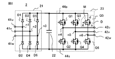
- FIG. 2 is a diagram showing the configuration of the power converter of FIG. 1
- FIG. 3 is a diagram showing the configuration of the voltage divider circuit of FIG. 4 is a diagram showing a first example of the injection waveform generator of FIG. 1
- FIG. 5 is a diagram showing a second example of the injection waveform generator of FIG. 1
- FIG. 6 is a diagram showing an injection waveform generator of FIG. It is a figure which shows the 3rd example of.
- FIG. 7 is a diagram showing the configuration of the second noise filter and the motor drive system according to the first embodiment, and FIG.
- FIG. 8 is a diagram showing the configuration of the third noise filter and the motor drive system according to the first embodiment. be.
- FIG. 9 is a diagram showing a configuration of a noise filter and a motor drive system of a comparative example.
- 10 is a diagram showing the core of the noise filter according to the first embodiment
- FIG. 11 is a cross-sectional view taken along the broken line shown by AA of FIG.
- FIG. 12 is a perspective view showing the core of the noise filter according to the first embodiment
- FIG. 13 is a perspective view showing the core of the noise filter of the comparative example.
- FIG. 14 is a diagram showing the configuration of the fourth noise filter and the motor drive system according to the first embodiment, and FIG.
- FIG. 15 is a diagram showing the configuration of the fifth noise filter and the motor drive system according to the first embodiment.
- FIG. 16 is a diagram showing a configuration of a sixth noise filter and a motor drive system according to the first embodiment.
- the noise filter 50 of the first embodiment is applied to an electric motor drive system 60 which is a system in which an induction motor 3 is controlled by a power converter 2 such as a voltage type PWM inverter in which a plurality of semiconductor elements perform switching operations.
- the motor drive system 60 includes an AC power source 1 such as a power system and a self-supporting voltage source, a power converter 2 that converts the AC power of the AC power source 1 into DC power, and an AC power source 1 that converts the DC power into AC power.
- a three-phase power line 4 connecting the power converter 2 and the power converter 2 a three-phase power line 5 connecting the power converter 2 and the induction motor 3, and a noise filter 50 are provided.
- the induction motor 3 is grounded by the ground wire 6.
- the ground potential that is, the ground potential, is the reference potential of the noise filter 50.
- the three-phase power line 4 includes a u-phase three-phase power line 4u, a v-phase three-phase power line 4v, and a w-phase three-phase power line 4w.
- the three-phase power line 5 includes a u-phase three-phase power line 5u, a v-phase three-phase power line 5v, and a w-phase three-phase power line 5w.
- the noise filter 50 includes a voltage detector 7, a voltage divider circuit 9, an injection waveform generator 10, and common mode transformers 11a and 11b.
- the power converter 2 is composed of a forward conversion circuit 21 composed of semiconductor elements, a capacitor 22 which is a storage element for storing DC power, and a reverse conversion circuit 23 which converts DC power into AC power. Be prepared.
- the forward conversion circuit 21 is, for example, a rectifier circuit, and includes six diodes D1, D2, D3, D4, D5, and D6.
- the inverse transformation circuit 23 includes six semiconductor elements Q1, Q2, Q3, Q4, Q5, and Q6.
- the three-phase power lines 4u, 4v, and 4w are connected to the AC input terminals 41u, 41v, and 41w of the power converter 2 at the other ends, respectively.
- the three-phase power lines 5u, 5v, and 5w whose one end is connected to the induction motor 3 are connected to the AC output terminals 42u, 42v, and 42w of the power converter 2 at the other ends, respectively.
- the forward conversion circuit 21 is a first series body which is a diode D1 and D2 connected in series between the high potential side wiring 44p and the low potential side wiring 44s, and a diode D3 and D4 connected in series.
- a second series body and a third series body which is a diode D5 and D6 connected in series are arranged.
- the connection point n1 between the diode D1 and the diode D2 is connected to the AC input terminal 41u.
- the connection point n2 between the diode D3 and the diode D4 is connected to the AC input terminal 41v
- the connection point n3 between the diode D5 and the diode D6 is connected to the AC input terminal 41w.
- the capacitor 22 is connected between the high potential side wiring 44p and the low potential side wiring 44s.
- the inverse conversion circuit 23 is composed of semiconductor elements Q1 and Q2 connected in series between the high potential side wiring 44p and the low potential side wiring 44s, a fourth series body, and semiconductor elements Q3 and Q4 connected in series.
- a fifth series body and a sixth series body, which are semiconductor elements Q5 and Q6 connected in series, are arranged.
- the connection point n4 between the semiconductor element Q1 and the semiconductor element Q2 is connected to the AC output terminal 42u.
- the connection point n5 between the semiconductor element Q3 and the semiconductor element Q4 is connected to the AC output terminal 42v, and the connection point n6 between the semiconductor element Q5 and the semiconductor element Q6 is connected to the AC output terminal 42w.
- semiconductor elements Q1, Q2, Q3, Q4, Q5, and Q6, for example, semiconductor elements for power such as MOSFET (Metal-Oxide-Semiconductor Field-Effect Transistor) and IGBT (Insulated Gate Bipolar Transistor) are used.
- FIG. 2 shows an example of MOSFET.
- the semiconductor elements Q1, Q2, Q3, Q4, Q5, and Q6 include a MOS transistor M and a diode D.
- the diode D may be an element different from the MOS transistor M, or may be a parasitic diode.
- the drain d of the semiconductor elements Q1, Q3, and Q5 is connected to the high potential side wiring 44p, and the sources s of the semiconductor elements Q2, Q4, and Q6 are connected to the low potential side wiring 44s.
- the source s of the semiconductor element Q1 and the drain d of the semiconductor element Q2 are connected, the source s of the semiconductor element Q3 and the drain d of the semiconductor element Q4 are connected, and the source s of the semiconductor element Q5 and the drain of the semiconductor element Q6 are connected.
- d is connected.
- a control signal is input from a control circuit (not shown) to the gate g of the semiconductor elements Q1, Q2, Q3, Q4, Q5, and Q6.
- the inverse conversion circuit 23 switches the semiconductor elements Q1, Q2, Q3, Q4, Q5, and Q6 based on the control signal from the control circuit to convert DC power into AC power.
- the voltage detector 7 that detects the common mode voltage Vci includes three capacitors 8 having equal capacities to each other, and one end of each capacitor 8 is connected to each phase of the three-phase power line 5. The other ends of the capacitors 8 are connected to each other at the connection point n7.
- the input terminal 94 is connected to the connection point n7 to which the other end of the capacitor 8 is connected, and the output terminal 95 is connected to the input terminal 51 of the injection waveform generator 10.
- the voltage divider circuit 9 divides the common mode voltage Vci, which is the input voltage between the wiring 24 at the ground potential and the input terminal 94, and outputs the divided voltage divider Vd as the output voltage.
- the voltage dividing circuit 9 includes, for example, a capacitor 91 and a series of resistors 92 and 93 connected in parallel to the capacitor 91. One end of the capacitor 91 and one end of the resistor 92 are connected to the input terminal 94, and the other end of the capacitor 91 and the other end of the resistor 93 are connected to the wiring 24 having a ground potential. The connection point to which the other end of the resistor 92 and one end of the resistor 93 are connected is connected to the output terminal 95.
- the voltage divider circuit 9 outputs the voltage divider voltage Vd obtained by dividing the common mode voltage Vci input to the input terminal 94 from the output terminal 95.
- the detected common mode voltage Vci is divided by the resistance ratio of the resistor 92 and the resistor 93.
- the voltage of the three-phase power lines 5u, 5v, and 5w, which are each phase of the three-phase power line 5, is divided by the impedance ratio of the capacitor 8 and the capacitor 91, and then divided by the resistance ratio of the resistor 92 and the resistor 93. It is output from the voltage divider circuit 9 as the pressure voltage Vd.
- the voltage dividing voltage Vd is input to the input terminal 51 of the injection waveform generator 10.
- the injection waveform generator 10 outputs a voltage whose band is limited and whose voltage value is adjusted based on the input voltage dividing voltage Vd from the output terminal 52.
- the output output from the output terminal 52 of the injection waveform generator 10 is input to the primary side of the common mode transformers 11a and 11b, that is, the primary winding.
- the common mode transformers 11a and 11b include a primary winding on the primary side and a secondary winding on the secondary side, and the secondary winding is each phase of the three-phase power line 5, three-phase power lines 5u, 5v, 5w. It is inserted in.
- the power converter 2 generates a common mode voltage Vci that changes in steps each time the semiconductor elements Q1 to Q6 perform switching operations.
- This common mode voltage Vci is detected by the voltage detector 7 and is divided into the voltage dividing voltage Vd by the voltage dividing circuit 9.
- the voltage dividing voltage Vd is band-limited by the injection waveform generator 10, and the output voltage Vp output after adjusting the voltage value is input to the primary windings of the common mode transformers 11a and 11b.
- the voltage generated in the secondary windings of the common mode transformers 11a and 11b, that is, the injection voltage Vs is adjusted so as to reduce the common mode voltage Vci generated in the power converter 2.
- the noise filter 50 of the first embodiment sets the output voltage Vp, which is a voltage opposite to the common mode voltage Vci and adjusted, based on the common mode voltage Vci detected by the voltage detector 7. Since the injection voltage Vs is superimposed on each phase of the three-phase power line 5 by inputting to the transformers 11a and 11b, the common mode voltage Vci can be suppressed. It will be described that the noise filter 50 of the first embodiment can suppress the common mode voltage Vci by using the small common mode transformers 11a and 11b even when the switching frequency of the power converter 2 is low.
- FIGS. 4 to 6 show first to third examples of the injection waveform generator 10.
- the injection waveform generator 10 of the first example shown in FIG. 4 includes a band limiter 12, an amplifier 13, and control power supplies 15a and 15b.
- the control power supply 15a supplies a positive side voltage
- the control power supply 15b supplies a negative side voltage. Since the band limiter 12 can apply only the frequency band to be reduced in the common mode voltage Vci to the common mode transformers 11a and 11b, the common mode transformers 11a and 11b can be miniaturized.
- the band limiter 12 may apply any of a bandpass filter, a lowpass filter, and a highpass filter as long as it can pass the target frequency band.
- the target frequency band of the band limiter 12 is set to a frequency band higher than 2 kHz, and a high-pass filter having a cutoff frequency is connected to a frequency lower than 2 kHz.
- the low frequency component of the voltage applied to 11b can be attenuated, and the common mode transformers 11a and 11b can be miniaturized.
- the common mode transformers 11a and 11b can be further reduced in size by connecting a high-pass filter having a cutoff frequency between 2 kHz and 10 kHz. Can be changed.
- the amplifier 13 shown in FIG. 4 is an example of an inverting amplifier circuit.
- the amplifier 13 includes an operational amplifier 19, resistors 16, 17, and 18.
- a ground potential is input to the positive input terminal of the operational amplifier 19 via a resistor 17.
- the output of the band limiter 12 is input to the negative input terminal of the operational amplifier 19 via the resistor 16, and the output of the operational amplifier 19 is input via the resistor 18.
- the gain Gi of the operational amplifier 19 is set by the voltage dividing ratio Rv of the voltage dividing circuit 9, the turns ratio Rr of the common mode transformers 11a and 11b, and the number of connected transformers Nt which is the number of the common mode transformers 11a and 11b to be connected.
- the injection voltage Vs which is the voltage superimposed on the u-phase, v-phase, and w-phase of the three-phase power line 5 via the secondary windings of the common mode transformers 11a and 11b, reduces the common mode voltage Vci, that is, the equation.
- the gain Gi, the voltage division ratio Rv, the turns ratio Rr, and the number of connected transformers Nt are set so that (3) is satisfied.
- Vt001 is an allowable value of the voltage difference. Equation (3) indicates that the absolute value of the difference between the common mode voltage Vci and the total injection voltage Vst is equal to or less than the allowable value Vt réelle.
- the total injection voltage Vst is a voltage obtained by adding the injection voltages Vs generated by the common mode transformers 11a and 11b.
- the total injection voltage Vst which is the total of the voltages superimposed on the u-phase, v-phase, and w-phase of the three-phase power line 5, is 2 ⁇ . It becomes Vs.
- the total injection voltage Vst which is the total of the voltages superimposed on the u-phase, v-phase, and w-phase of the three-phase power line 5, is expressed by the equation (4) when the number of connected transformers Nt is used. In the case of FIG. 1, the number of connected transformers Nt is 2.
- Vst Nt ⁇ Vs ⁇ ⁇ ⁇ (4)
- the voltage dividing ratio Rv of the voltage dividing circuit 9 can be expressed by the equation (5).
- the turns ratio Rr of the common mode transformers 11a and 11b can be expressed by the equation (6), where N1 and N2 are the turns of the primary winding and the secondary winding, respectively.
- Rv Vci / Vd ⁇ ⁇ ⁇ (5)
- Rr N2 / N1 ... (6)
- the noise filter 50 of the first embodiment has a small common mode transformers 11a and 11b with a total injection voltage Vst of the u-phase, v-phase, and w-phase of the three-phase power line 5. Can be superimposed on. Therefore, the noise filter 50 of the first embodiment can suppress the common mode voltage by using a small common mode transformer even when the switching frequency is low. It will be described later that the common mode transformer can be made smaller by reducing the injection voltage Vs.
- the injection waveform generator 10 of the second example will be described.
- the injection waveform generator 10 of the second example is different from the injection waveform generator 10 of the first example in that a current buffer 14 is added between the output terminal and the output terminal 52 of the amplifier 13.
- the output terminal of the amplifier 13 is a connection point between the wiring that transmits the output of the operational amplifier 19 and the resistor 18.
- the injection waveform generator 10 of the second example can increase the current capacity indicating the amount of current supply as compared with the injection waveform generator 10 of the first example.
- the current buffer 14 includes, for example, two transistors BT1 and BT2 connected in series.
- the collector c of the transistor BT1 is connected to the control power supply 15a, the emitter e of the transistor BT1 is connected to the emitter e of the transistor BT2, and the collector c of the transistor BT2 is connected to the control power supply 15b.
- the output of the amplifier 13 is input to the base b of the transistors BT1 and BT2, and the emitter e of the transistors BT1 and BT2 is connected to the output terminal 52.
- the amplifier 13 shows an example of an inverting amplifier circuit, but the amplifier 13 may be a non-inverting amplifier circuit.
- the injection waveform generator 10 of the third example shown in FIG. 6 is an example of a non-inverting amplifier circuit.
- the output of the band limiter 12 is input to the positive input terminal of the operational amplifier 19 via the resistor 17.
- the ground potential is input to the negative input terminal of the operational amplifier 19 via the resistor 16, and the output of the operational amplifier 19 is input via the resistor 18.
- the amplifier 13 is a non-inverting amplifier circuit, as shown in FIG. 7, the connection to the primary winding of the common mode transformers 11a and 11b is changed in reverse, and the injection voltage Vs which is the voltage output to the secondary winding is changed. Is set to reduce the common mode voltage Vci.
- the noise filter 50 of the first embodiment will be described while comparing it with the noise filter 100 of the comparative example.
- the noise filter 100 of the comparative example shown in FIG. 9 includes one common mode transformer 101, and the motor drive system 110 of the comparative example includes a noise filter 100.
- the output voltage Vpe is output from the injection waveform generator 102 to the primary winding of the common mode transformer 101, and the injection voltage Vse is superimposed on the u-phase, v-phase, and w-phase of the three-phase power line 5. ..
- the noise filter 100 of the comparative example is different from the noise filter 50 of the first embodiment in that it includes one common mode transformer 101 and the injection waveform generator 10 is changed to the injection waveform generator 102.
- the injection waveform generator 102 has the same configuration as the injection waveform generator 10, but the gain Gi and the like differ depending on the value of the output voltage Vpe.
- the noise filter 100 of the comparative example has a connected transformer number Nt of 1. In order to achieve the same reduction in common mode voltage even if the number of common mode transformers is different, the total injection voltage Vst of the same value is required. Therefore, as can be seen from the equation (4), in the noise filter 100 of the comparative example, the injection voltage Vs superposed on each phase of the three-phase power line 5 by the noise filter 50 of the first embodiment in which the number of connected transformers Nt is 2.
- the first method is to make the output voltage Vpe the same as the output voltage Vp and double the turns ratio Rr of the common mode transformer 101.
- the second method is to make the turns ratio Rr of the common mode transformer 101 the same as the turn ratio Rr of the common mode transformers 11a and 11b, and to make the output voltage Vpe twice the output voltage Vp.
- the common mode transformers 11a and 11b include one primary winding and three secondary windings.
- the cores of the common mode transformers 11a and 11b are, for example, the toroidal type core 28 shown in FIG. Since the noise filter 50 of the first embodiment includes two common mode transformers 11a and 11b, it includes two cores 28 as shown in FIG.
- the common mode transformer 101 of the comparative example is also the same as the common mode transformers 11a and 11b. Since the noise filter 100 of the comparative example includes one common mode transformer 101, it includes one core 29 as shown in FIG. The size of the core will be described later.
- the first method in order to increase the turns ratio Rr of the common mode transformer 101, there are a method of reducing the number of turns of the primary winding and a method of increasing the number of turns of the secondary winding.
- the exciting current of the common mode transformer 101 increases and the magnetic flux also increases.
- the secondary winding since the secondary winding has three windings having a wire diameter equivalent to that of the three-phase power line 5, the inner diameter required for the core becomes large. Therefore, as a result, the core becomes large.
- a voltage equal to or higher than the voltage values of the control power supplies 15a and 15b is generated in the secondary winding of the common mode transformer 101 as the injection voltage Vse, it is inevitable to increase the size of the core.
- the second method in order to apply a high voltage to the common mode transformer 101, a control power supply and a high withstand voltage element that output a high voltage are required. Further, since the voltage-time product in the common mode transformer 101 becomes large, it is necessary to increase the cross-sectional area of the core and the number of turns of the primary winding in order to avoid magnetic saturation of the core. In order to keep the turns ratio Rr constant, the number of turns of the secondary winding also increases, and as a result, even when a high voltage is applied to the common mode transformer 101, the size of the core is increased.
- the noise filter 50 of the first embodiment is provided with a plurality of common mode transformers 11a and 11b, so that the injection voltage Vs generated by one common mode transformer can be reduced. Therefore, unlike the noise filter 100 of the comparative example, the noise filter 50 of the first embodiment does not need to increase the cross-sectional area of the core of the common mode transformers 11a and 11b, and increases the inner diameter of the core in order to increase the number of turns. There is no need, and the core can be miniaturized. Further, in the noise filter 50 of the first embodiment, the voltage applied to the common mode transformers 11a and 11b, that is, the output voltage Vp may be a low voltage, and the voltage time product can be reduced, so that the core can be miniaturized. In addition, in the noise filter 50 of the first embodiment, the voltages of the control power supplies 15a and 15b applied to the injection waveform generator 10 may be low, and the injection waveform generator 10 can be configured by a low withstand voltage element. Is.
- the common mode suppression circuit of Patent Document 1 has one common mode transformer having a turns ratio Rr of 1. As described above, when the switching frequency is low, the time product of the magnetic flux generated in the core becomes large, so that the core used for the common mode transformer to generate the same voltage in the secondary winding becomes large. With one common mode transformer, this size increase becomes remarkable. Since the noise filter 50 of the first embodiment includes two common mode transformers 11a and 11b, when the total injection voltage Vst superimposed on the three-phase power line 5 by the common mode suppression circuit of Patent Document 1 is the same, each common mode The injection voltage Vs on which the transformers 11a and 11b are superimposed can be set to Vst / 2.
- the noise filter 50 of the first embodiment a common mode transformer having a core smaller than that of the common mode suppression circuit of Patent Document 1 can be used.
- the size of the core in the noise filter 50 of the first embodiment will be described with reference to FIGS. 10 to 13.
- the core in the noise filter 50 of the first embodiment is, for example, the toroidal type core 28 shown in FIG. 10 as described above. Since the noise filter 50 of the first embodiment includes two common mode transformers 11a and 11b, it includes two cores 28 as shown in FIG. Since the noise filter 100 of the comparative example includes one common mode transformer 101, it includes one core 29 as shown in FIG.
- the inner diameter of the core 28 is l, the outer diameter is L, and the width (thickness) is h.
- the cross-sectional area of the core 28 is S. In FIG. 11, the left side is the inside of the core 28, and the right side is the outside of the core 28.
- the cross-sectional area S can be reduced while keeping the magnetic flux density B and the number of turns N1 on the primary side constant.
- the core 28 is considered.
- the cross-sectional area Se and the volume v1 of the core 29 can be expressed by the equations (12) and (13).
- the cross-sectional area Se of the core 29 is the area of the cross section along the broken line shown by AA when the core 28 in FIG. 10 is used as the core 29.
- the width of the core 29 is the same h as the width of the core 28.
- Se h ⁇ (Le-l) / 2 ...
- v1 ⁇ ⁇ h ⁇ (Le 2- l 2 ) / 4 ⁇ ⁇ ⁇ (13)
- the cross-sectional area S and volume v2 of the core 28 can be expressed by equations (14) and (15).
- S h ⁇ (L ⁇ l) / 2 ⁇ ⁇ ⁇ (14)
- v2 ⁇ ⁇ h ⁇ (L 2- l 2 ) / 4 ⁇ ⁇ ⁇ (15)
- the common mode transformers 11a and 11b in the noise filter 50 of the first embodiment have the outer diameter L of one core 28 smaller than the outer diameter Le under the condition that the magnetic flux density B and the inner diameter l are constant.
- the total volume or total size of the core 28 can be reduced while maintaining the cross-sectional area S of one core 28 at half the cross-sectional area Se of the core 29.
- the constant inner diameter l is due to the fact that the number of turns N1 is constant and the required inner diameter is constant.
- the noise filter 50 of the first embodiment can make the total size of the two common mode transformers smaller than that of the common mode transformer of Patent Document 1.
- the noise filter 50 of the first embodiment uses two small common mode transformers, so that the degree of freedom in arranging the common mode transformers is higher than that of the common mode suppression circuit of Patent Document 1. Therefore, the noise filter 50 of the first embodiment enables more efficient component arrangement than the common mode suppression circuit of Patent Document 1, and can realize a small noise filter. Further, the noise filter 50 of the first embodiment is more than the common mode transformer of Patent Document 1 by applying a band limitation to the voltage dividing voltage Vd to eliminate the frequency at which the injection waveform generator 10 has a great influence on the core increase. It can be made even smaller.
- the common of Patent Document 1 is performed even if the band limitation for excluding the frequency having a great influence on the core increase is not performed.
- the common mode transformers 11a and 11b can be made smaller than the mode transformer.
- the common mode suppression circuit of Patent Document 1 requires a high withstand voltage transistor because the power of the control power supply is the power of the DC power supply on the input side of the inverter.
- the injection voltage Vs becomes 1/2 of the injection voltage of the common mode suppression circuit of Patent Document 1, and the output voltage Vp output by the injection waveform generator 10 is patented.
- the voltage can be made lower than that of the common mode suppression circuit of 1. Therefore, the injection waveform generator 10 can be configured with a low withstand voltage element.
- the noise filter 50 of the first embodiment can make the common mode transformers 11a and 11b smaller than the noise filter 100 of the comparative example and the common mode transformer of the common mode suppression circuit of Patent Document 1.
- the voltage detector 7 shown in FIG. 1 is connected to the three-phase power line 5, the voltage detector 7 can also be connected to the three-phase power line 4 as shown in FIG.
- the power converter 2 also generates a common mode voltage Vci in the three-phase power line 4. Even in this case, since the common mode voltage Vci detected from the three-phase power line 4 is equivalent to the common mode voltage Vci detected from the three-phase power line 5, the equation (3) may be satisfied. Further, although the example in which the common mode transformers 11a and 11b are inserted into the three-phase power line 5 is shown, the common mode transformers 11a and 11b can also be inserted into the three-phase power line 4 as shown in FIG.
- the common mode voltage Vci in the three-phase power line 5 can be reduced.
- FIG. 15 shows an example in which the voltage detector 7 is connected to the three-phase power line 4, the voltage detector 7 may be connected to the three-phase power line 5. Further, as shown in FIG. 16, the positions of the common mode transformers 11a and 11b and the voltage detector 7 may be exchanged.
- the noise filter 50 of the first example shown in FIG. 1 has a feedforward configuration, while the noise filter 50 of the sixth example shown in FIG. 16 has a feedback configuration.
- the voltage dividing circuit 9 As an example of the voltage dividing circuit 9, an example including a capacitor 91 and resistors 92 and 93 is shown, but the voltage dividing circuit 9 is not limited to this.
- the voltage dividing circuit 9 can be configured with only a capacitor 91 in which two capacitors are connected in series, a configuration with only resistors 92 and 93, and a configuration in which the number of capacitors and resistors is increased.
- the noise filter 50 of the first embodiment is a noise filter that reduces the common mode voltage Vci generated by the power converter 2 that performs power conversion by the switching operation of the semiconductor elements Q1 to Q6.
- the noise filter 50 outputs a voltage divider 7 that detects the common mode voltage Vci generated by the power converter 2 and a voltage divider Vd that is obtained by dividing the common mode voltage Vci detected by the voltage detector 7.
- the circuit 9 a plurality of common mode transformers 11a and 11b for superimposing an injection voltage Vs (Vsa, Vsb) having a polarity opposite to the common mode voltage Vci on the output or input of the power converter 2, and a plurality of common mode transformers 11a and 11b based on the voltage dividing voltage Vd.
- the injection waveform generator 10 for generating an output voltage Vp to be output to the primary side of the common mode transformers 11a and 11b of the above is provided.
- the injection waveform generator 10 has an output voltage in which the difference between the total injection voltage Vst obtained by adding the injection voltages Vs (Vsa, Vsb) superimposed by the plurality of common mode transformers 11a and 11b and the common mode voltage Vci is equal to or less than the allowable value Vt réelle. Generate Vp.
- the noise filter 50 of the first embodiment includes a plurality of common mode transformers 11a and 11b, and the injection waveform generator 10 superimposes the injection voltage Vs (Vsa, Vsb) on the plurality of common mode transformers 11a and 11b.
- the common mode voltage is used by using the small common mode transformers 11a and 11b. Vci can be suppressed.
- FIG. 17 is a diagram showing the configuration of the first noise filter and the motor drive system according to the second embodiment.
- FIG. 18 is a diagram showing a first example of the first injection waveform generator of FIG. 17, and
- FIG. 19 is a diagram showing a first example of the second injection waveform generator of FIG. 20 is a diagram showing a second example of the first injection waveform generator of FIG. 17, and
- FIG. 21 is a diagram showing a second example of the second injection waveform generator of FIG. 22 is a diagram showing a third example of the first injection waveform generator of FIG. 17, and
- FIG. 23 is a diagram showing a third example of the second injection waveform generator of FIG.
- FIG. 24 is a diagram showing a fourth example of the first injection waveform generator of FIG. 17, and FIG.
- FIG. 25 is a diagram showing a fourth example of the second injection waveform generator of FIG.
- FIG. 26 is a diagram showing a fifth example of the first injection waveform generator of FIG. 17, and
- FIG. 27 is a diagram showing a fifth example of the second injection waveform generator of FIG.
- FIG. 28 is a diagram showing a sixth example of the first injection waveform generator of FIG. 17, and
- FIG. 29 is a diagram showing a sixth example of the second injection waveform generator of FIG.
- FIG. 30 is a diagram showing the configuration of the second noise filter and the motor drive system according to the second embodiment, and
- FIG. 31 is a diagram showing the configuration of the third noise filter and the motor drive system according to the second embodiment. be.
- the output voltages Vpa, Vpb, and Vpc are output to the three common mode transformers 11a, 11b, and 11c by the two injection waveform generators 10a and 10b, and the three commons. It differs from the noise filter 50 of the first embodiment in that the mode transformers 11a, 11b, and 11c generate injection voltages Vsa, Vsb, and Vsc in each phase of the three-phase power line 5.
- the injection waveform generator 10 shown in FIG. 4 is a band in which the band limiter 12 passes through a low frequency band and reduces a high frequency band.
- the injection waveform generator 10 shown in FIG. 4 is a band in which the band limiter 12 passes through a high frequency band and reduces a low frequency band. It differs in that it has been changed to the limiter 33.
- the injection waveform generator 10a outputs an output voltage Vpa from the output terminal 52a and outputs an output voltage Vpb from the output terminal 52b.
- the injection waveform generator 10b outputs an output voltage Vpc from the output terminal 52.
- the wiring 24 which is the ground potential is omitted.
- the wiring 24 having the ground potential is omitted.
- the noise filter 50 of the second embodiment includes an injection waveform generator including two waveform generators (injection waveform generators 10a and 10b).
- the injection waveform generator 10a is set to amplify only the low frequency band and decrease the high frequency band.
- the injection waveform generator 10b is set to amplify only the high frequency band and decrease the low frequency band. That is, the injection waveform generator 10a outputs the output voltages Vpa and Vpb in the low frequency band to the common mode transformers 11a and 11b, and the injection waveform generator 10b outputs the output voltage Vpc in the high frequency band to the common mode transformer 11c.
- the frequency bands of the output voltages Vpa and Vpb are different from those of the output voltage Vpc.
- a low frequency band voltage is applied to the common mode transformers 11a and 11b connected to the injection waveform generator 10a, and a high frequency band voltage is applied to the common mode transformer 11c connected to the injection waveform generator 10b.
- the output voltages Vpa and Vpb may have different voltage values from the output voltage Vpc depending on the frequency band.
- the common mode transformer 11c to which the high frequency band is applied can be downsized as compared with the common mode transformers 11a and 11b.
- the common mode transformer 11c can be miniaturized by reducing the turns N1 and N2 of the common mode transformer 11c instead of reducing the cross-sectional area S of the core 28.
- the number of turns N1 and N2 is reduced, the inner diameter l required for the core 28 becomes smaller.
- the cross-sectional area S of the core 28 is constant, the outer diameter L can be reduced by reducing the inner diameter l, and as a result, the common mode transformer 11c can be miniaturized. These can be performed at the same time, and when the voltage time product in the transformer is small, the cross-sectional area S of the core 28 is reduced, the turns N1 and N2 are reduced, and the outer diameter L and inner diameter l of the core 28 are reduced. Is also possible.
- transformers are affected by self-resonance due to inductance and parasitic capacitance, impedance decreases in the high frequency band, and exciting current increases. Since this self-resonant frequency differs depending on the core material, the exciting current is excited by using a core material having a high self-resonance frequency and high impedance even in the high frequency band for the common mode transformer 11c to which a voltage in the high frequency band is applied. Can be reduced. This makes it possible to reduce the power supply capacity indicating the power supply amount of the control power supplies 15a and 15b that supply power to the injection waveform generator 10b.
- the two injection waveform generators 10a and 10b have different configurations, and the three common mode transformers 11a, 11b, and 11c have different configurations, and the applied voltages are in the low frequency band and the high frequency band.
- the power supply capacities of the control power supplies 15a and 15b are reduced, for example, by increasing the gain Gi of the amplifier 13, the output voltages Vpa, Vpb and Vpc are made the same as when the power supply capacities of the control power supplies 15a and 15b are not reduced. be able to.
- the injection waveform generator 10 shown in FIG. 5 is a band in which the band limiter 12 passes through the low frequency band and reduces the high frequency band. It is changed to the limiter 32 and differs in that it has two output terminals 52a and 52b.
- the injection waveform generator 10 shown in FIG. 5 is a band in which the band limiter 12 passes through the high frequency band and reduces the low frequency band. It differs in that it has been changed to the limiter 33.
- the injection waveform generator 10a outputs an output voltage Vpa from the output terminal 52a and outputs an output voltage Vpb from the output terminal 52b.
- the injection waveform generator 10b outputs an output voltage Vpc from the output terminal 52.
- a current buffer 14 is provided between the output terminal of the amplifier 13 and the output terminals 52a and 52b. It differs in that it has been added.
- a current buffer 14 is added between the output terminal and the output terminal 52 of the amplifier 13 as in the first example of the second injection waveform generator 10b. It differs in that.
- the second example of the first injection waveform generator 10a and the second example of the second injection waveform generator 10b show the current supply amount by the current buffer 14 as compared with the injection waveform generators 10a and 10b of the first example. It is possible to increase the current capacity.
- the third example of the first injection waveform generator 10a shown in FIG. 22 has no band limiter 32 on the input terminal 51 side as the first example of the first injection waveform generator 10a shown in FIG.
- the difference is that the band limiters 32a and 32b are arranged between the output terminals of the amplifier 13 and the output terminals 52a and 52b, respectively.
- the frequency band of the band limiter 32a and the frequency band of the band limiter 32b may be the same or different.
- the output voltages Vpa and Vpb having different frequency bands can be output.
- the frequency band of the output voltages Vpa and Vpb is a frequency band lower than the output voltage Vpc.
- the third example of the second injection waveform generator 10b shown in FIG. 23 is different from the first example of the second injection waveform generator 10b shown in FIG. 19 without the band limiter 33 on the input terminal 51 side.
- the difference is that the band limiter 33 is arranged between the output terminal and the output terminal 52 of the amplifier 13.
- the third example of the first injection waveform generator 10a is the output terminal of the amplifier 13 and the input side of the band limiters 32a and 32b.
- the difference is that the current buffer 14 is added between the two.
- the fourth example of the second injection waveform generator 10b shown in FIG. 25 is that the third example of the second injection waveform generator 10b is between the output terminal of the amplifier 13 and the input side of the band limiter 33.
- the difference is that the current buffer 14 is added to.
- the fourth example of the first injection waveform generator 10a and the fourth example of the second injection waveform generator 10b show the current supply amount by the current buffer 14 as compared with the injection waveform generators 10a and 10b of the third example. It is possible to increase the current capacity.
- the fourth example of the first injection waveform generator 10a shown in FIG. 24 is an example in which the current buffer 14 is arranged between the output terminal of the amplifier 13 and the input side of the band limiters 32a and 32b.
- the current buffer 14 may be arranged between the output side of the band limiters 32a and 32b and the output terminals 52a and 52b.
- the fifth example of the first injection waveform generator 10a shown in FIG. 26 is different from the third example of the first injection waveform generator 10a in that the current is between the output side of the band limiter 32a and the output terminal 52a. The difference is that a buffer 14a is added and a current buffer 14b is added between the output side of the band limiter 32b and the output terminal 52b.
- the current buffers 14a and 14b can increase the current capacity indicating the current supply amount as compared with the injection waveform generator 10a of the third example.
- the fourth example of the second injection waveform generator 10b shown in FIG. 25 is an example in which the current buffer 14 is arranged between the output terminal of the amplifier 13 and the input side of the band limiter 33.
- the current buffer 14 may be arranged between the output side of the band limiter 33 and the output terminal 52.
- the fifth example of the second injection waveform generator 10b shown in FIG. 27 is different from the third example of the second injection waveform generator 10b in that the current is between the output side of the band limiter 33 and the output terminal 52. The difference is that the buffer 14 is added.
- the current buffer 14 can increase the current capacity indicating the current supply amount as compared with the injection waveform generator 10b of the third example.
- the sixth example of the first injection waveform generator 10a shown in FIG. 28 is a band limiter between the input terminal 51 and the input side of the amplifier 13 with the third example of the first injection waveform generator 10a. It differs in that 32c is arranged.
- the third example of the second injection waveform generator 10b is a band limiter between the input terminal 51 and the input side of the amplifier 13. It differs in that 34 is arranged.
- the frequency band of the band limiter 32c is a lower frequency band than the band limiters 33 and 34 in the second injection waveform generator 10b, similarly to the band limiters 32a and 32b.
- the frequency band of the band limiter 34 is a higher frequency band than the band limiters 32a, 32b, 32c in the first injection waveform generator 10a, similarly to the band limiter 33.
- the sixth example of the first injection waveform generator 10a is also provided with the band limiter 32c on the input side, the band limiters 32a and 32b on the output side can be miniaturized. Therefore, the sixth example of the first injection waveform generator 10a is the third example of the first injection waveform generator 10a provided with two band limiters 32a, 32b by the small band limiters 32a, 32b, 32c. The total power consumption of the band limiter can be reduced more than that of. In the sixth example of the second injection waveform generator 10b, since the band limiter 34 is also provided on the input side, the band limiter 33 on the output side can be made smaller. Therefore, the sixth example of the first injection waveform generator 10b has a smaller band than the third example of the second injection waveform generator 10b including one band limiter 33 due to the small band limiters 33 and 34. The total power consumption of the limiter can be reduced.
- FIG. 17 shows a case where there are two injection waveform generators and three common mode transformers, but the number of each is not limited.
- the output voltages Vpa and Vpc may be output from the two injection waveform generators 10a and 10b for the two common mode transformers 11a and 11c.
- the second noise filter 50 of the second embodiment shown in FIG. 30 is different from the noise filter 50 of the first embodiment shown in FIG. 1 by two injection waveform generators 10a and 10b and two common mode transformers 11a.
- 11c is different in that the output voltages Vpa and Vpc are output.
- the output voltages Vpa and Vpc may be output from one injection waveform generator 10a for the two common mode transformers 11a and 11c.
- the injection waveform generator 10a to which the band limiters 32a and 32b are provided on the output terminals 52a and 52b is applied to the injection waveform generator 10a shown in FIGS. 22, 24, 26 and 28. can.
- the injection waveform generators 10a and 10b have shown the case where the frequency bands are different, that is, the frequency characteristics are different, the same gain and frequency characteristics can be configured.
- the noise filter 50 of the second embodiment has substantially the same operation as the noise filter 50 of the first embodiment, and thus has the same effect as the noise filter 50 of the first embodiment.
- the injection waveform generators 10a and 10b may be provided with amplifiers 13 having different gains, and may output output voltages Vpa and Vpc of different voltage values.
- the common mode transformers 11a, 11b, and 11c show the case where the core material, the outer diameter L of the core 28, the inner diameter l, the cross-sectional area S, and the number of turns N1 and N2 are different. It can also be configured with l, the cross-sectional area S, and the number of turns N1 and N2.
- noise filter 50 of the first embodiment and the second embodiment is applied to an electric motor drive system 60 equipped with a power converter 2 that converts three-phase AC power to three-phase AC power via DC power.
- the noise filter 50 of the first embodiment and the second embodiment can also be applied to a system equipped with a power converter that generates a common mode voltage by a switching operation of a semiconductor element.
- the power converter 2 may be an isolated DC-DC converter. In this case, the AC power supply 1 becomes a DC power supply, and the induction motor 3 becomes a DC motor.
- the noise filter 50 of the second embodiment includes the common mode transformer 11a to which the output voltage Vpa in the low frequency band is input and the common mode transformer 11c to which the output voltage Vpc in the high frequency band is input.
- the common mode transformer 11c for the high frequency band can be made smaller than the common mode transformer 11a for the low frequency band. Therefore, the noise filter 50 of the second embodiment can be made smaller than the common mode transformer of Patent Document 1, and the common mode voltage can be suppressed by using the small common mode transformer even when the switching frequency is low.
- the noise filter 50 of the second embodiment is provided with a plurality of common mode transformers of a low frequency band which are larger than the common mode transformer 11c of the high frequency band, so that each noise filter 50 is provided as described in the first embodiment. Since the injection voltages Vsa and Vsb of the above are smaller, the common mode transformers 11a and 11b can be made smaller, and can be made smaller than the common mode transformer of Patent Document 1.
- Vci Common mode voltage
- Vd voltage dividing voltage
- Vp, Vpa, Vpb, Vpc output voltage
- Vs, Vsa, Vsb, Vsc injection voltage
- Vst total injection voltage
Landscapes
- Engineering & Computer Science (AREA)
- Power Engineering (AREA)
- Physics & Mathematics (AREA)
- Electromagnetism (AREA)
- Inverter Devices (AREA)
- Power Conversion In General (AREA)
Priority Applications (5)
| Application Number | Priority Date | Filing Date | Title |
|---|---|---|---|
| US17/920,076 US11996769B2 (en) | 2020-06-04 | 2020-06-04 | Noise filter |
| CN202080101303.6A CN115699546B (zh) | 2020-06-04 | 2020-06-04 | 噪声滤波器 |
| PCT/JP2020/022062 WO2021245865A1 (ja) | 2020-06-04 | 2020-06-04 | ノイズフィルタ |
| JP2022529240A JP7309067B2 (ja) | 2020-06-04 | 2020-06-04 | ノイズフィルタ |
| EP20939355.2A EP4164100A4 (en) | 2020-06-04 | 2020-06-04 | NOISE FILTER |
Applications Claiming Priority (1)
| Application Number | Priority Date | Filing Date | Title |
|---|---|---|---|
| PCT/JP2020/022062 WO2021245865A1 (ja) | 2020-06-04 | 2020-06-04 | ノイズフィルタ |
Publications (1)
| Publication Number | Publication Date |
|---|---|
| WO2021245865A1 true WO2021245865A1 (ja) | 2021-12-09 |
Family
ID=78830195
Family Applications (1)
| Application Number | Title | Priority Date | Filing Date |
|---|---|---|---|
| PCT/JP2020/022062 Ceased WO2021245865A1 (ja) | 2020-06-04 | 2020-06-04 | ノイズフィルタ |
Country Status (5)
| Country | Link |
|---|---|
| US (1) | US11996769B2 (https=) |
| EP (1) | EP4164100A4 (https=) |
| JP (1) | JP7309067B2 (https=) |
| CN (1) | CN115699546B (https=) |
| WO (1) | WO2021245865A1 (https=) |
Cited By (1)
| Publication number | Priority date | Publication date | Assignee | Title |
|---|---|---|---|---|
| JPWO2023166544A1 (https=) * | 2022-03-01 | 2023-09-07 |
Families Citing this family (1)
| Publication number | Priority date | Publication date | Assignee | Title |
|---|---|---|---|---|
| EP3934049A1 (de) * | 2020-06-29 | 2022-01-05 | Siemens Aktiengesellschaft | Filtervorrichtung |
Citations (7)
| Publication number | Priority date | Publication date | Assignee | Title |
|---|---|---|---|---|
| JPH1094244A (ja) * | 1996-09-18 | 1998-04-10 | Okayama Univ | アクティブコモンモードキャンセラ |
| JP2000201044A (ja) * | 1999-01-07 | 2000-07-18 | Mitsubishi Electric Corp | コモンモ―ドノイズ抑制装置 |
| JP2000244272A (ja) * | 1999-02-24 | 2000-09-08 | Toshiba Corp | ノイズフィルタ |
| JP2001333582A (ja) * | 2000-05-19 | 2001-11-30 | Fuji Electric Co Ltd | 電力変換器のノイズ低減装置 |
| JP2017038500A (ja) * | 2015-08-12 | 2017-02-16 | 三星電子株式会社Samsung Electronics Co.,Ltd. | 伝導性ノイズ抑制回路及びインバータ装置 |
| JP6491349B2 (ja) | 2015-11-06 | 2019-03-27 | 国立大学法人北海道大学 | 電力変換装置 |
| JP2019080469A (ja) * | 2017-10-27 | 2019-05-23 | 三菱電機株式会社 | ノイズ低減装置 |
Family Cites Families (10)
| Publication number | Priority date | Publication date | Assignee | Title |
|---|---|---|---|---|
| WO2000007274A2 (en) * | 1998-07-28 | 2000-02-10 | Pdl Electronics Limited | Active common-mode compensation for multi-phase inverters |
| JP3466118B2 (ja) | 1999-08-31 | 2003-11-10 | 三菱電機株式会社 | インバータ式駆動装置の漏洩電流低減フィルタ |
| JP2005094918A (ja) * | 2003-09-17 | 2005-04-07 | Fuji Electric Holdings Co Ltd | 電力変換装置のノイズ低減回路 |
| US20060034364A1 (en) * | 2004-08-13 | 2006-02-16 | Breitzmann Robert J | Carrier synchronization to reduce common mode voltage in an AC drive |
| JP2006136058A (ja) * | 2004-11-02 | 2006-05-25 | Toshiba Corp | ノイズフィルタ |
| JP5263663B2 (ja) * | 2008-08-28 | 2013-08-14 | 富士電機株式会社 | 伝導性ノイズフィルタ |
| CN102474171B (zh) * | 2009-08-19 | 2015-08-05 | 株式会社安川电机 | 输出滤波器和具有该输出滤波器的电动机驱动系统 |
| JP5993886B2 (ja) * | 2014-03-04 | 2016-09-14 | 株式会社豊田中央研究所 | ノイズフィルタ |
| JP6769170B2 (ja) | 2015-09-01 | 2020-10-14 | 富士電機株式会社 | アクティブノイズ抑制装置 |
| DE102018121934A1 (de) * | 2018-09-07 | 2020-03-12 | Avl Software And Functions Gmbh | Aktiver Filter mit mehreren Verstärkerpfaden |
-
2020
- 2020-06-04 WO PCT/JP2020/022062 patent/WO2021245865A1/ja not_active Ceased
- 2020-06-04 EP EP20939355.2A patent/EP4164100A4/en active Pending
- 2020-06-04 CN CN202080101303.6A patent/CN115699546B/zh active Active
- 2020-06-04 US US17/920,076 patent/US11996769B2/en active Active
- 2020-06-04 JP JP2022529240A patent/JP7309067B2/ja active Active
Patent Citations (7)
| Publication number | Priority date | Publication date | Assignee | Title |
|---|---|---|---|---|
| JPH1094244A (ja) * | 1996-09-18 | 1998-04-10 | Okayama Univ | アクティブコモンモードキャンセラ |
| JP2000201044A (ja) * | 1999-01-07 | 2000-07-18 | Mitsubishi Electric Corp | コモンモ―ドノイズ抑制装置 |
| JP2000244272A (ja) * | 1999-02-24 | 2000-09-08 | Toshiba Corp | ノイズフィルタ |
| JP2001333582A (ja) * | 2000-05-19 | 2001-11-30 | Fuji Electric Co Ltd | 電力変換器のノイズ低減装置 |
| JP2017038500A (ja) * | 2015-08-12 | 2017-02-16 | 三星電子株式会社Samsung Electronics Co.,Ltd. | 伝導性ノイズ抑制回路及びインバータ装置 |
| JP6491349B2 (ja) | 2015-11-06 | 2019-03-27 | 国立大学法人北海道大学 | 電力変換装置 |
| JP2019080469A (ja) * | 2017-10-27 | 2019-05-23 | 三菱電機株式会社 | ノイズ低減装置 |
Non-Patent Citations (1)
| Title |
|---|
| See also references of EP4164100A4 |
Cited By (4)
| Publication number | Priority date | Publication date | Assignee | Title |
|---|---|---|---|---|
| JPWO2023166544A1 (https=) * | 2022-03-01 | 2023-09-07 | ||
| WO2023166544A1 (ja) * | 2022-03-01 | 2023-09-07 | 三菱電機株式会社 | ノイズフィルタ |
| EP4489276A4 (en) * | 2022-03-01 | 2025-04-02 | Mitsubishi Electric Corporation | NOISE FILTER |
| JP7714112B2 (ja) | 2022-03-01 | 2025-07-28 | 三菱電機株式会社 | ノイズフィルタ |
Also Published As
| Publication number | Publication date |
|---|---|
| US11996769B2 (en) | 2024-05-28 |
| JPWO2021245865A1 (https=) | 2021-12-09 |
| CN115699546B (zh) | 2026-02-27 |
| CN115699546A (zh) | 2023-02-03 |
| EP4164100A4 (en) | 2023-07-12 |
| JP7309067B2 (ja) | 2023-07-14 |
| US20230179176A1 (en) | 2023-06-08 |
| EP4164100A1 (en) | 2023-04-12 |
Similar Documents
| Publication | Publication Date | Title |
|---|---|---|
| US9130542B1 (en) | Noise filter | |
| US6617814B1 (en) | Integrated DC link choke and method for suppressing common-mode voltage in a motor drive | |
| US10992217B2 (en) | Insulated power source and power conversion device | |
| US11088614B2 (en) | Conductive noise suppressor, power converter, and motor device | |
| US10700625B2 (en) | Power conversion device | |
| JP6568743B2 (ja) | 伝導性ノイズ抑制回路及びインバータ装置 | |
| WO2011125944A1 (ja) | 漏れ電流低減装置 | |
| US7132812B1 (en) | Integrated DC link choke and method for suppressing common-mode voltage in a motor drive | |
| JP2010284029A (ja) | インバータ駆動用電源回路 | |
| CN114079383B (zh) | Dc到dc转换器 | |
| JP7309067B2 (ja) | ノイズフィルタ | |
| US6987372B1 (en) | Integrated DC link choke and method for suppressing common-mode voltage in a motor drive | |
| JPWO2016027374A1 (ja) | 電力変換装置 | |
| JP7714112B2 (ja) | ノイズフィルタ | |
| WO2023073984A1 (ja) | コモンモードフィルタ | |
| JP5070929B2 (ja) | 能動フィルタ装置及び電力変換装置 | |
| JPWO2021245865A5 (https=) | ||
| JP5840514B2 (ja) | 漏れ電流抑制回路 | |
| JP2018098309A (ja) | リアクトル及びコンバータ装置 | |
| JP7511669B2 (ja) | ノイズフィルタ | |
| JP2605456Y2 (ja) | インバータ回路 | |
| JP2008043096A (ja) | 電力変換装置 |
Legal Events
| Date | Code | Title | Description |
|---|---|---|---|
| 121 | Ep: the epo has been informed by wipo that ep was designated in this application |
Ref document number: 20939355 Country of ref document: EP Kind code of ref document: A1 |
|
| ENP | Entry into the national phase |
Ref document number: 2022529240 Country of ref document: JP Kind code of ref document: A |
|
| NENP | Non-entry into the national phase |
Ref country code: DE |
|
| ENP | Entry into the national phase |
Ref document number: 2020939355 Country of ref document: EP Effective date: 20230104 |